slvu906 | ti.com - analog
TRANSCRIPT

User's GuideSLVU906–April 2013
Low IDDQ PMIC for Battery Energy HarvestingApplications
The TPS65290 is an integrated PMIC for flow-meter system, low-power energy-harvesting, medical,consumer and commercial battery operation application. This EVM helps the evaluation of TPS65290 foryour actual system. TPS65290 can be controlled by SPI using the USB2ANY kit.
Contents1 Introduction .................................................................................................................. 3
1.1 I/O Description ...................................................................................................... 32 Test Procedure .............................................................................................................. 4
2.1 Hardware and Software Set Up .................................................................................. 42.2 EVM Test ............................................................................................................ 72.3 GUI User’s Guide .................................................................................................. 92.4 Simulation Model and Test Result ............................................................................. 11
3 Schematic .................................................................................................................. 144 Board Layout ............................................................................................................... 15
4.1 PCB Layout ........................................................................................................ 165 Bench Test Setup Conditions ............................................................................................ 206 Bill of Materials ............................................................................................................. 21
List of Figures
1 USB2ANY Interface......................................................................................................... 5
2 10 Pins of USB2ANY Indication........................................................................................... 6
3 GUI Main Window........................................................................................................... 7
4 Set Up for the USB2ANY .................................................................................................. 8
5 Unlock the USB2ANY ...................................................................................................... 9
6 Read the Data ............................................................................................................. 10
7 Write the Register ......................................................................................................... 11
8 Buck Boost Efficiency, VIN = 3.6 V, VO = 4.5 V ........................................................................ 12
9 Buck Boost Efficiency, VIN = 3.6 V, VO = 2.8 V ........................................................................ 12
10 Buck Boost Load Regulation, VIN = 3.6 V, VO = 4.5 V, PFM Mode ................................................. 13
11 Buck Boost Line Regulation, VO = 2.8 V, IO = 5 mA................................................................... 13
12 TPS65290 Schematic..................................................................................................... 14
13 Placement ................................................................................................................. 15
14 Board Layout (Top Layer) ................................................................................................ 16
15 Board Layout (Middle 2nd) Layer......................................................................................... 16
16 Board Layout (Middle 3rd) Layer ......................................................................................... 17
17 Board Layout (Bottom Layer) ............................................................................................ 18
18 Headers Description and Jumper Placement.......................................................................... 20
List of Tables
1 Power Connection .......................................................................................................... 3
2 Header Descriptions ........................................................................................................ 3
1SLVU906–April 2013 Low IDDQ PMIC for Battery Energy Harvesting ApplicationsSubmit Documentation Feedback
Copyright © 2013, Texas Instruments Incorporated

www.ti.com
3 Test Points ................................................................................................................... 4
4 J4 10-PIN Connection of USB2ANY ..................................................................................... 6
5 Jumper Connections for Low-IDDQ Measurement ..................................................................... 8
6 Default Value of EVM ...................................................................................................... 9
2 Low IDDQ PMIC for Battery Energy Harvesting Applications SLVU906–April 2013Submit Documentation Feedback
Copyright © 2013, Texas Instruments Incorporated

www.ti.com Introduction
1 Introduction
1.1 I/O Description
Table 1. Power Connection
NUMBER TYPE LOCATION SIGNAL COMMENT
J1 I N Input supply Connection to input supply
J2 I N SPI Connection to SPI interface board
J3 O S LDO and MICRO outputs Connection to MICRO and LDO output
J7 O E Buck-boost output Connection to buck-boost output
Table 2. Header Descriptions
NUMBER FUNCTION LOCATION PLACEMENT COMMENT
Connect analog VIN(pin #2) to theJP1 Supply connect NW Fit in most casesmain power connector(J1)
Connect VMAX to the joint of 1µF andJP4 LDO input connector W Fit in most casesLDO input
Fit only when Buck mini isJP8 Buck mini connection S Connection to Buck mini inductor used
Connection to PWR_LDO2 output If Not connect in BUCKminiJP8A PWR_LDO2 connector S buck-mini option available leave open mode
When not fitted adds a 1-Ω resistanceto the output capacitor, allowing for a Fit according to testJP10 Buck MINI output ESR S predictable ESR value for the requirementBUCKmini mode. Fit for low IQQ LDOor zero leak circuit.
Connect to VMICRO for enablingserial communication. Conect to GND Fit according to testJP11 CE S for Vmicro only mode for lowest IDDQ requirementconsumption.
Connect to GND to disable BB (I2C Fit according to testJP13 BB enable SE can enable it). Connect to VMICRO to requirementenable BB.
3SLVU906–April 2013 Low IDDQ PMIC for Battery Energy Harvesting ApplicationsSubmit Documentation Feedback
Copyright © 2013, Texas Instruments Incorporated

Test Procedure www.ti.com
Table 3. Test Points
TP NAME LOCATION SIGNAL
TP1 PWR_VIN W PWR_VIN input pin 1
TP2 GND W
TP3 PWR_VMAX W PWR_VMAX PIN 3
TP4 VMAX W VMAX PIN 4
TP5 LDO IN W LDO input pin 5
TP6 LDO_OUT W LDO output pin 6
TP7 PWR_LDO1 W PWR_LDO1 switch output pin 7
TP8 GND W
TP9 GND E
TP12 PWR_BB2 E PWR_BB2 switch pin 12
TP14 PWR_BB1 E PWR_BB1 switch pin 13
TP15 BB_OUT E Buck boost output pin 15
TP16 BB_LX2 N LX2 node BB (pin 16)
TP18 BB_LX1 N LX1 node BB (pin 18)
TP20 INT N Interruption pin 20
TP21 MISO N MISO pin 21 SPI
2 Test Procedure
2.1 Hardware and Software Set Up
2.1.1 Power Supply
A power supply capable of supplying 2.2 V - 5 V, 3 A, is required. A short cable from the power supply tothe EVM input is recommended. If long line is a must, a 2,200-µF capacitor is suggested at the input forbetter input supply stability.
2.1.2 Load
Use electronic load or other variable resistor to evaluate different load conditions.
2.1.3 Input Current Meters
The current meters must have low impedance when measuring the efficiency to decrease the voltage dropaffect. Placing a 2,200-µF capacitor at the input side of the EVM will guarantee the low impedance.
2.1.4 USB2ANY Communication Kit
The USB2ANY serves as an interface adapter between a host PC and a TPS65290 EVM. Thecommunication between the USB2ANY and the host PC is via USB, while the communication between theUSB2ANY and the TPS56290 EVM is via an SPI. The USB2ANY hardware is based on the TIMSP430F5529 16bit Microcontroller with integrated USB 2.0.
4 Low IDDQ PMIC for Battery Energy Harvesting Applications SLVU906–April 2013Submit Documentation Feedback
Copyright © 2013, Texas Instruments Incorporated

www.ti.com Test Procedure
Figure 1. USB2ANY Interface
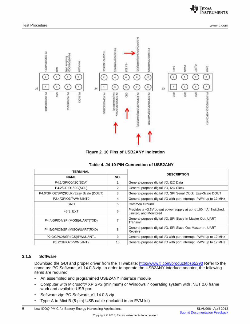
The center 10 pins of the USB2ANY is used to connect to JP2 in the EVM with the provided 10-pin flatcable. The pin definitions of the center 10-pin connectors of the USB2ANY box are shown in Figure 2.
5SLVU906–April 2013 Low IDDQ PMIC for Battery Energy Harvesting ApplicationsSubmit Documentation Feedback
Copyright © 2013, Texas Instruments Incorporated
Test Procedure www.ti.com
Figure 2. 10 Pins of USB2ANY Indication
Table 4. J4 10-PIN Connection of USB2ANY
TERMINALDESCRIPTION
NAME NO.
P4.1/GPIO0/I2C(SDA) 1 General-purpose digital I/O, I2C Data
P4.2/GPIO1/I2C(SCL) 2 General-purpose digital I/O, I2C Clock
P4.0/GPIO2/SPI(SCLK)/Easy Scale (DOUT) 3 General-purpose digital I/O, SPI Serial Clock, EasyScale DOUT
P2.4/GPIO3/PWM3/INT0 4 General-purpose digital I/O with port Interrupt, PWM up to 12 MHz
GND 5 Common Ground
Provides a +3.3V output power supply at up to 100 mA. Switched,+3.3_EXT 6 Limited, and Monitored
General-purpose digital I/O, SPI Slave In Master Out, UARTP4.4/GPIO4/SPI(MOSI)/UART(TXD) 7 Transmit
General-purpose digital I/O, SPI Slave Out Master In, UARTP4.5/GPIO5/SPI(MISO)/UART(RXD) 8 Receive
P2.0/GPIO6/SPI(CS)/PWM1/INT1 9 General-purpose digital I/O with port Interrupt, PWM up to 12 MHz
P1.2/GPIO7/PWM0/INT2 10 General-purpose digital I/O with port Interrupt, PWM up to 12 MHz
2.1.5 Software
Download the GUI and proper driver from the TI website: http://www.ti.com/product/tps65290 Refer to thename as: PC-Software_v1.14.0.3.zip. In order to operate the USB2ANY interface adapter, the followingitems are required:
• An assembled and programmed USB2ANY interface module
• Computer with Microsoft® XP SP2 (minimum) or Windows 7 operating system with .NET 2.0 framework and available USB port
• Software zip: PC-Software_v1.14.0.3.zip
• Type-A to Mini-B (5-pin) USB cable (Included in an EVM kit)
6 Low IDDQ PMIC for Battery Energy Harvesting Applications SLVU906–April 2013Submit Documentation Feedback
Copyright © 2013, Texas Instruments Incorporated

www.ti.com Test Procedure
• A 10-pin cable connector (Included in an EVM kit)
Then install the software step by step:
1. Extract the zip. The folder contains the USB2ANY_GUI.exe and support files. The USB interfaceadapter is recognized by a PC as a generic human interface device (HID), which is supported by thebuilt-in USB/HID drivers of the Windows® operating system. Therefore, plug it and it will playautomatically, no proprietary USB driver is required.
2. Plug in the USB cable to both the PC and the USB interface adapter. The status LED of the adapterwill flash several times and then will illuminate steadily indicating that the USB2ANY is functioningproperly and is ready to use.If the green LED fails to flash several times illuminating steadily, or fails to illuminate at all, check toensure the USB cable is securely connected. If the connection is secure, try a different USB portand/or rebooting the computer. If that does not fix the issue then contact TI technical support.
3. Run the USB2ANY_GUI.exe software. The status bar on the bottom left should show USB2ANY:Detected. If it shows USB2ANY: NOT Detected, follow the procedure in step 2. above until the statusbar indicates that the USB2ANY has been detected.
Figure 3. GUI Main Window
2.2 EVM Test
2.2.1 Power Up Sequence1. Connect USB2ANY to a host computer by an USB cable
2. Launch USB2ANY GUI software as described in the following section
3. Connect a 10-pin flat cable between the USB2ANY and an EVM
4. Power up the input of EVM
7SLVU906–April 2013 Low IDDQ PMIC for Battery Energy Harvesting ApplicationsSubmit Documentation Feedback
Copyright © 2013, Texas Instruments Incorporated

Test Procedure www.ti.com
2.2.2 USB2ANY GUI Launch
Change as the red box selection as shown figure Figure 4. Change the divider of the input frequency tothe same as that in Figure 3 to make the communication speed 4 kHz. Start with low communicationfrequency for easier verification.
Make sure each red box is properly modified.
Then, clock “Set SPI” to make the change enabled.
“Set SPI” should be clicked everytime after any in the red boxes are changed.
Probe that voltages of CS, SCL, MOSI and MISO are all zero.
Figure 4. Set Up for the USB2ANY
2.2.3 Test With SPI Interface Buffer Disabled for Lowest IDDQ Mode
When JP11 is connected to GND, TPS65290 provides only Vmicro voltage and other blocks are disabledto maintain minimum power consupmtion. Therefore the SPI communication doesn’t work at Vmicro only.Use Table 5 for the proper jumper connection for Vmicro only mode.
Table 5. Jumper Connections for Low-IDDQ Measurement
Vmicro MODE FIT THESE JUMPERS DO NOT FIT THESE JUMPERS JP11, JP13
TPS65290BM JP1, JP4, JP8 JP8A, JP10 GND
TPS65290ZB JP1, JP4, JP10, JP8A JP8 GND
TPS65290LM JP1, JP4, JP10, JP8A JP8 GND
The default value of the micro and buck/boost are described in Table 6. The buck-boost can be enabledby connecting JP13 to Vmicro. Keep in mind that the loading of an oscilloscope probe or a multi-meter canincrease the input current.
8 Low IDDQ PMIC for Battery Energy Harvesting Applications SLVU906–April 2013Submit Documentation Feedback
Copyright © 2013, Texas Instruments Incorporated

www.ti.com Test Procedure
Table 6. Default Value of EVM
DEFAULT OUTPUT VALUENOTES
MIN TYP MAX
Vmicro 1.98 V 2.2 V 2.42 V
To enable the buck/boost, JP13 shouldVbb_out 3.977 V 4.1 V 4.223 V connect as ENBB-VMICRO
2.2.4 Test With the SPI iIIerface
Connect JP11 to Vmicro to enable SPI interface buffers and the digital block. Follow Section 2.3 fordetailed GUI instruction.
2.3 GUI User’s Guide
2.3.1 GUI User’s Guide
Write “1 0 80” on the read box.
Click the “Write and Read” button.
Figure 5. Unlock the USB2ANY
2.3.2 Read the Register
Fill in the red box then click the “Write and Read” button.
The first character is the register address to read. Keep the second and the third characters to be “80 00”.
The figure below shows reading the address of 03, and then gets the data back as 08, which means thatthe buck/boost output voltage is 2.6V now.
9SLVU906–April 2013 Low IDDQ PMIC for Battery Energy Harvesting ApplicationsSubmit Documentation Feedback
Copyright © 2013, Texas Instruments Incorporated

Test Procedure www.ti.com
Figure 6. Read the Data
2.3.3 Write the Register
Fill in the red box then click the “Write and Read” button.
The first character is the register address to write, and the third character is the value to write in. Keep thesecond character to be “00”.
The figure below shows writing the HEX 12 to address 03, to change the output voltage to 4V, after settingthe data you want to write, and click the “Write and Read”.
10 Low IDDQ PMIC for Battery Energy Harvesting Applications SLVU906–April 2013Submit Documentation Feedback
Copyright © 2013, Texas Instruments Incorporated

www.ti.com Test Procedure
Figure 7. Write the Register
2.4 Simulation Model and Test Result
2.4.1 Spice Model
This device has one similar function spice model of buck/boost. Download at:http://www.ti.com/product/tps63020
And it’s convenient to use TINA-TI software to simulate under varying conditions. Download this tool at:http://www.ti.com/tool/tina-ti
11SLVU906–April 2013 Low IDDQ PMIC for Battery Energy Harvesting ApplicationsSubmit Documentation Feedback
Copyright © 2013, Texas Instruments Incorporated

0%
10%
20%
30%
40%
50%
60%
70%
80%
90%
100%
0 50 100 150 200 250 300 350 400 450 500
Io(mA)
0%
10%
20%
30%
40%
50%
60%
70%
80%
90%
100%
0 50 100 150 200 250 300 350 400 450 500
Io (mA)
Test Procedure www.ti.com
2.4.2 Main Features
2.4.2.1 Efficiency
Figure 8. Buck Boost Efficiency, VIN = 3.6 V, VO = 4.5 V
Figure 9. Buck Boost Efficiency, VIN = 3.6 V, VO = 2.8 V
12 Low IDDQ PMIC for Battery Energy Harvesting Applications SLVU906–April 2013Submit Documentation Feedback
Copyright © 2013, Texas Instruments Incorporated
2.75
2.76
2.77
2.78
2.79
2.8
2.81
2.82
2.83
2.84
2.85
3 3.5 4 4.5 5 5.5 6 6.5
VLD
O(V
)
Vin(V)
4.38
4.40
4.42
4.44
4.46
4.48
4.50
0 50 100 150 200 250 300 350 400 450 500
Io (mA)
www.ti.com Test Procedure
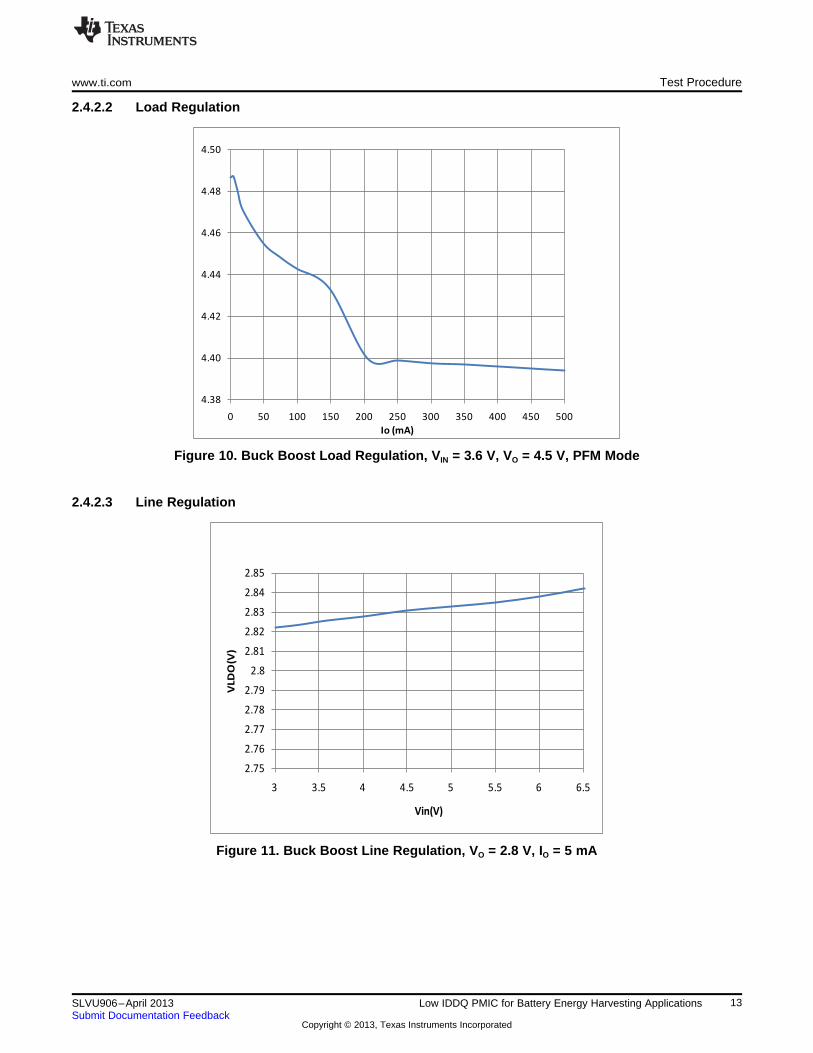
2.4.2.2 Load Regulation
Figure 10. Buck Boost Load Regulation, VIN = 3.6 V, VO = 4.5 V, PFM Mode
2.4.2.3 Line Regulation
Figure 11. Buck Boost Line Regulation, VO = 2.8 V, IO = 5 mA
13SLVU906–April 2013 Low IDDQ PMIC for Battery Energy Harvesting ApplicationsSubmit Documentation Feedback
Copyright © 2013, Texas Instruments Incorporated
Schematic www.ti.com
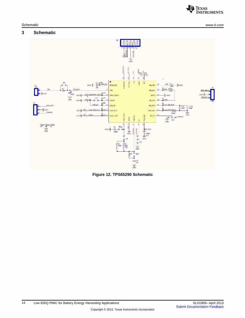
3 Schematic
Figure 12. TPS65290 Schematic
14 Low IDDQ PMIC for Battery Energy Harvesting Applications SLVU906–April 2013Submit Documentation Feedback
Copyright © 2013, Texas Instruments Incorporated

www.ti.com Board Layout
4 Board Layout
Figure 13. Placement
15SLVU906–April 2013 Low IDDQ PMIC for Battery Energy Harvesting ApplicationsSubmit Documentation Feedback
Copyright © 2013, Texas Instruments Incorporated

Board Layout www.ti.com
4.1 PCB Layout
Figure 14. Board Layout (Top Layer)
16 Low IDDQ PMIC for Battery Energy Harvesting Applications SLVU906–April 2013Submit Documentation Feedback
Copyright © 2013, Texas Instruments Incorporated

www.ti.com Board Layout
Figure 15. Board Layout (Middle 2nd) Layer
17SLVU906–April 2013 Low IDDQ PMIC for Battery Energy Harvesting ApplicationsSubmit Documentation Feedback
Copyright © 2013, Texas Instruments Incorporated
Board Layout www.ti.com
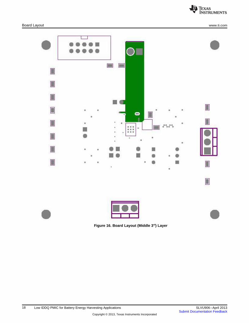
Figure 16. Board Layout (Middle 3rd) Layer
18 Low IDDQ PMIC for Battery Energy Harvesting Applications SLVU906–April 2013Submit Documentation Feedback
Copyright © 2013, Texas Instruments Incorporated
www.ti.com Board Layout
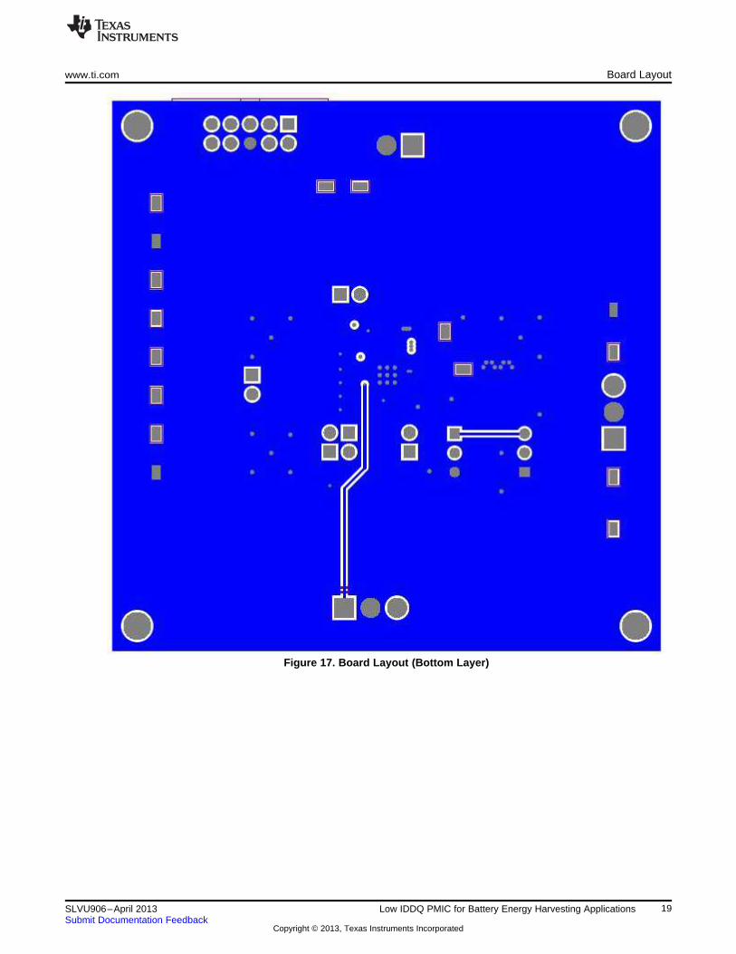
Figure 17. Board Layout (Bottom Layer)
19SLVU906–April 2013 Low IDDQ PMIC for Battery Energy Harvesting ApplicationsSubmit Documentation Feedback
Copyright © 2013, Texas Instruments Incorporated

Vin
+
SPI Interface
BBout
N
Test
Points
LDOout VmicroGND
PWR_BB1
GND
Switch point
LX1, L2
Bench Test Setup Conditions www.ti.com
5 Bench Test Setup Conditions
Figure 18. Headers Description and Jumper Placement
20 Low IDDQ PMIC for Battery Energy Harvesting Applications SLVU906–April 2013Submit Documentation Feedback
Copyright © 2013, Texas Instruments Incorporated

www.ti.com Bill of Materials
6 Bill of Materials
Qty Designator Value Footprint Manufacturer Part Number Description
4 C1, C7, C10, C4 1uF 0603 TDK Corporation C1608X7R1A105K CAP CER 1.0UF 10V X7R 0603
C0603C104K8RAC CAP .10UF 10V CERAMIC X7R6 C2, C3, C8, C12, C14 100nF 0603 Kemet TU 0603
CAP CER 2.2UF 10V X7R 20%1 C6 2.2uF 0603 Kemet C1608X7R1A225M 0603
C2012X5R336M122 C15, C15A 33uF 0805 TDK Corporation CAP CER 33UF 10V X5R 20% 08055AC
On Shore TERMINAL BLOCK 3.5MM 2POS1 J1 ED1514 TB_2X3.5MM ED555/2DSTechnology Inc PCB
ED555/3D On Shore TERMINAL BLOCK 3.5MM 3POS2 J3,J7 TB_3X3.5MM ED555/3DSS Technology Inc PCB
JP1, JP4, JP8, JP8A, CONN HEADER 2POS .100 VERT5 JMP0.2 Molex Inc 22-10-2021JP10 GOLD
CONN HEADER 3POS .100 VERT2 JP11, JP13 JMP0.3 Molex Inc 22-10-2031 GOLD
Abracon ASPI-0418FS- INDUCTOR SHLD POWER 3.3UH1 L1 3.3uH 4mmx4mm Corporation 3R3M-T3 SMD
GLFR1608T330M-1 L2 33uH 0603 TDK Corporation INDUCTOR 33UH 60MA 20% 0603LR
47uH GLFR2012T470M-1 L3 0805 TDK Corporation INDUCTOR 47UH 60MA 20% 0805(DNI) LR
RESISTOR 1.0 OHM 1/10W 5%1 R10 1 0603 Panasonic ECG ERJ-3GEYJ1R0V 0603
TP1, TP2, TP3, TP4,TP5, TP6, TP7, TP8,
16 TP9, TP12, TP14, TP_1030 Keystone 1030 TEST POINT SLOTTEDTP15, TP16, TP18,TP20, TP21
RHF (PQFP-1 U1 Texas Instruments TPS6529024)
0 Ohm1 R2 0603(DNI)
Sullins Connector SBH11-PBPC-D05- CONN HEADER 2.54mm 10POS1 J2 NA 5x2 header Solutions ST-BK GOLD
EMK107BBJ106M1 C21 10uF 0603 Taiyo Yuden CAP CER 10UF 16V 20% X5R 0603A-T
21SLVU906–April 2013 Low IDDQ PMIC for Battery Energy Harvesting ApplicationsSubmit Documentation Feedback
Copyright © 2013, Texas Instruments Incorporated

IMPORTANT NOTICE
Texas Instruments Incorporated and its subsidiaries (TI) reserve the right to make corrections, enhancements, improvements and otherchanges to its semiconductor products and services per JESD46, latest issue, and to discontinue any product or service per JESD48, latestissue. Buyers should obtain the latest relevant information before placing orders and should verify that such information is current andcomplete. All semiconductor products (also referred to herein as “components”) are sold subject to TI’s terms and conditions of salesupplied at the time of order acknowledgment.
TI warrants performance of its components to the specifications applicable at the time of sale, in accordance with the warranty in TI’s termsand conditions of sale of semiconductor products. Testing and other quality control techniques are used to the extent TI deems necessaryto support this warranty. Except where mandated by applicable law, testing of all parameters of each component is not necessarilyperformed.
TI assumes no liability for applications assistance or the design of Buyers’ products. Buyers are responsible for their products andapplications using TI components. To minimize the risks associated with Buyers’ products and applications, Buyers should provideadequate design and operating safeguards.
TI does not warrant or represent that any license, either express or implied, is granted under any patent right, copyright, mask work right, orother intellectual property right relating to any combination, machine, or process in which TI components or services are used. Informationpublished by TI regarding third-party products or services does not constitute a license to use such products or services or a warranty orendorsement thereof. Use of such information may require a license from a third party under the patents or other intellectual property of thethird party, or a license from TI under the patents or other intellectual property of TI.
Reproduction of significant portions of TI information in TI data books or data sheets is permissible only if reproduction is without alterationand is accompanied by all associated warranties, conditions, limitations, and notices. TI is not responsible or liable for such altereddocumentation. Information of third parties may be subject to additional restrictions.
Resale of TI components or services with statements different from or beyond the parameters stated by TI for that component or servicevoids all express and any implied warranties for the associated TI component or service and is an unfair and deceptive business practice.TI is not responsible or liable for any such statements.
Buyer acknowledges and agrees that it is solely responsible for compliance with all legal, regulatory and safety-related requirementsconcerning its products, and any use of TI components in its applications, notwithstanding any applications-related information or supportthat may be provided by TI. Buyer represents and agrees that it has all the necessary expertise to create and implement safeguards whichanticipate dangerous consequences of failures, monitor failures and their consequences, lessen the likelihood of failures that might causeharm and take appropriate remedial actions. Buyer will fully indemnify TI and its representatives against any damages arising out of the useof any TI components in safety-critical applications.
In some cases, TI components may be promoted specifically to facilitate safety-related applications. With such components, TI’s goal is tohelp enable customers to design and create their own end-product solutions that meet applicable functional safety standards andrequirements. Nonetheless, such components are subject to these terms.
No TI components are authorized for use in FDA Class III (or similar life-critical medical equipment) unless authorized officers of the partieshave executed a special agreement specifically governing such use.
Only those TI components which TI has specifically designated as military grade or “enhanced plastic” are designed and intended for use inmilitary/aerospace applications or environments. Buyer acknowledges and agrees that any military or aerospace use of TI componentswhich have not been so designated is solely at the Buyer's risk, and that Buyer is solely responsible for compliance with all legal andregulatory requirements in connection with such use.
TI has specifically designated certain components as meeting ISO/TS16949 requirements, mainly for automotive use. In any case of use ofnon-designated products, TI will not be responsible for any failure to meet ISO/TS16949.
Products Applications
Audio www.ti.com/audio Automotive and Transportation www.ti.com/automotive
Amplifiers amplifier.ti.com Communications and Telecom www.ti.com/communications
Data Converters dataconverter.ti.com Computers and Peripherals www.ti.com/computers
DLP® Products www.dlp.com Consumer Electronics www.ti.com/consumer-apps
DSP dsp.ti.com Energy and Lighting www.ti.com/energy
Clocks and Timers www.ti.com/clocks Industrial www.ti.com/industrial
Interface interface.ti.com Medical www.ti.com/medical
Logic logic.ti.com Security www.ti.com/security
Power Mgmt power.ti.com Space, Avionics and Defense www.ti.com/space-avionics-defense
Microcontrollers microcontroller.ti.com Video and Imaging www.ti.com/video
RFID www.ti-rfid.com
OMAP Applications Processors www.ti.com/omap TI E2E Community e2e.ti.com
Wireless Connectivity www.ti.com/wirelessconnectivity
Mailing Address: Texas Instruments, Post Office Box 655303, Dallas, Texas 75265Copyright © 2013, Texas Instruments Incorporated