small l big problemsll processors solve big...
TRANSCRIPT
ll l BIG PROBLEMSsmall processors solve BIG PROBLEMS
Chris RowenFounder and CTO
Tensilica IncTensilica, Inc.
10 May 2011
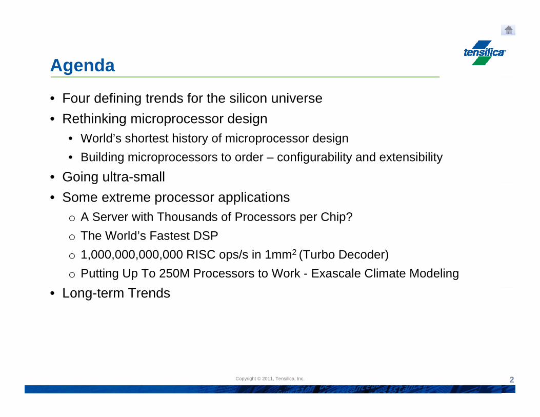
Agenda
• Four defining trends for the silicon universe• Rethinking microprocessor design
• World’s shortest history of microprocessor design• Building microprocessors to order – configurability and extensibility
• Going ultra-smallg• Some extreme processor applications
o A Server with Thousands of Processors per Chip?o The World’s Fastest DSPo The World s Fastest DSPo 1,000,000,000,000 RISC ops/s in 1mm2 (Turbo Decoder)o Putting Up To 250M Processors to Work - Exascale Climate Modeling
• Long-term Trends
Copyright © 2010, Tensilica, Inc.Copyright © 2011, Tensilica, Inc. 2
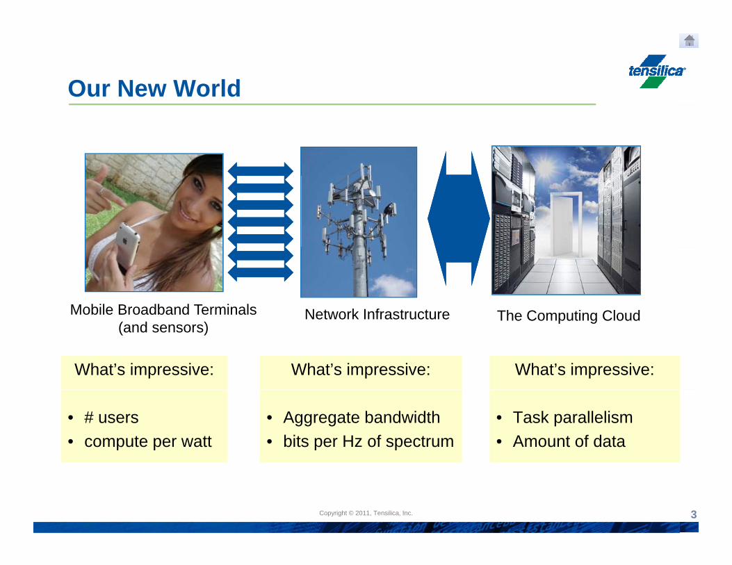
Our New World
Mobile Broadband Terminals Network Infrastructure The Computing Cloud
What’s impressive:
(and sensors)Network Infrastructure The Computing Cloud
What’s impressive: What’s impressive:
• # users• compute per watt
• Aggregate bandwidth• bits per Hz of spectrum
• Task parallelism• Amount of data
Copyright © 2010, Tensilica, Inc.Copyright © 2011, Tensilica, Inc. 3
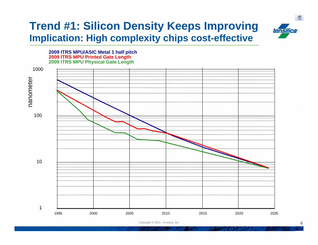
Trend #1: Silicon Density Keeps ImprovingImplication: High complexity chips cost-effective
2009 ITRS MPU/ASIC Metal 1 half pitch2009 ITRS MPU Printed Gate Length2009 ITRS MPU Physical Gate Length
1000
nano
met
er
100
10
Copyright © 2010, Tensilica, Inc.Copyright © 2011, Tensilica, Inc. 4
11995 2000 2005 2010 2015 2020 2025
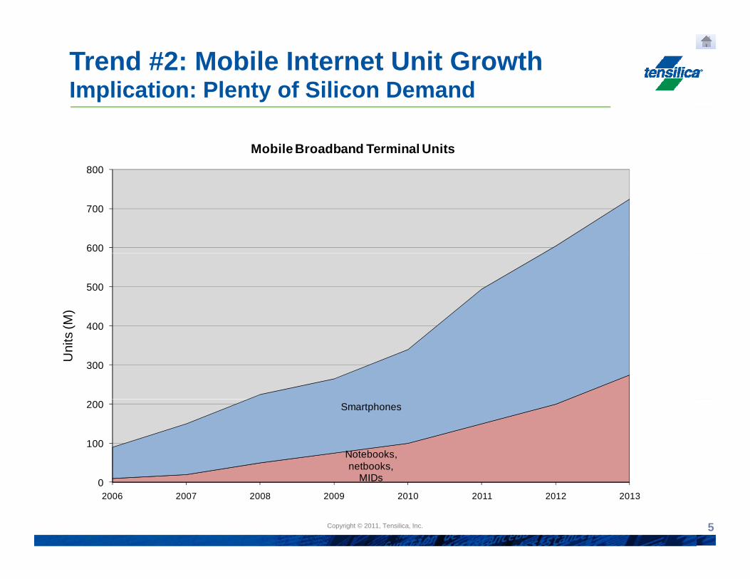
Trend #2: Mobile Internet Unit GrowthImplication: Plenty of Silicon Demand
800
Mobile Broadband Terminal Units
600
700
400
500
(M)
300
400
Uni
ts (
Notebooks, netbooks,
Smartphones
100
200
Copyright © 2010, Tensilica, Inc.Copyright © 2011, Tensilica, Inc. 5
MIDs02006 2007 2008 2009 2010 2011 2012 2013
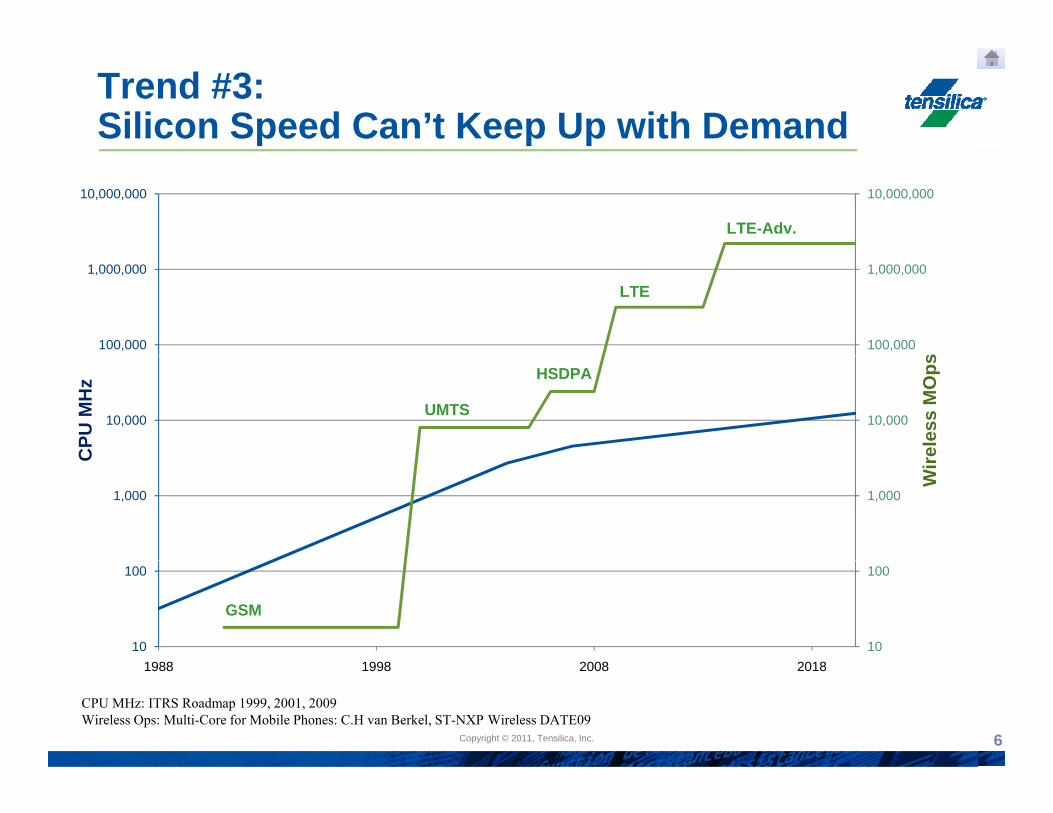
Trend #3: Silicon Speed Can’t Keep Up with Demand
10,000,00010,000,000
CPU MHz LTE-Adv.
100,000
1,000,000
100,000
1,000,000
s
LTE
10,00010,000
rele
ss M
Ops
CPU
MH
z HSDPA
UMTS
1,0001,000
WirC
10
100
10
100
1988 1998 2008 2018
GSM
Copyright © 2010, Tensilica, Inc.Copyright © 2011, Tensilica, Inc. 6
1988 1998 2008 2018
CPU MHz: ITRS Roadmap 1999, 2001, 2009Wireless Ops: Multi-Core for Mobile Phones: C.H van Berkel, ST-NXP Wireless DATE09
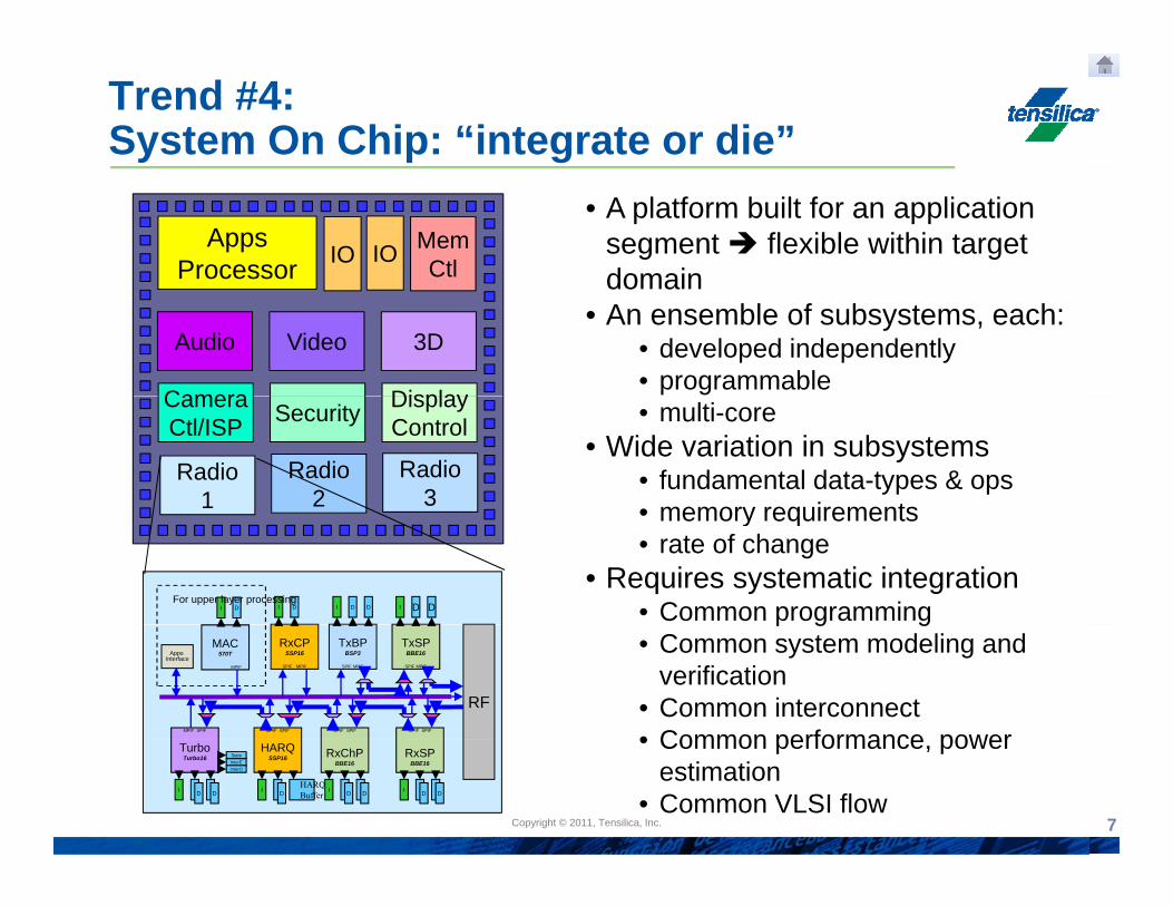
Trend #4:System On Chip: “integrate or die”
• A platform built for an application segment flexible within target domain
Apps Processor IO Mem
CtlIOdomain
• An ensemble of subsystems, each:• developed independently• programmable
Audio Video 3D
Camera Display • multi-core• Wide variation in subsystems
• fundamental data-types & ops• memory requirements
Radio1
Radio3
Radio2
Camera Ctl/ISP Security Display
Control
• memory requirements• rate of change
• Requires systematic integration• Common programmingI D DI D DI DI D
For upper layer processing
p g g• Common system modeling and
verification• Common interconnect • Common performance powerMPIF SPIFMPIF SPIFMPIF SPIFMPIF SPIF
Apps Interface
TxSPBBE16
SPIF MPIF
TxBPBSP3
SPIF MPIF
RxCPSSP16
SPIF MPIF
RF
MAC570T
MPIF
Copyright © 2010, Tensilica, Inc.Copyright © 2011, Tensilica, Inc. 7
• Common performance, power estimation
• Common VLSI flow
RxSPBBE16
I D D
RxChPBBE16
I D D
HARQSSP16
IHARQBufferD
TurboTurbo16
I D D
StateInterEInterO
I
PC++
memoryI TLB
PC++ PC[1]++PC[0]++
Basic micro-controller
Micro-code
General register file
Data width:4 8 16 32…
next PCPC++
memory
mPC++
mgmtTLB
PC++
branch memory
PC predict
branch memory
thread selectPC predict
Floating point
General register file
Cache and memory protect
Pipelined load/store arch
Imemory
microcodememoryImemory
memorymgmt
I TLB
cache missengine
I tags
Imemory
memorymgmt
I TLB
Superscalar (static or dyn.)
Symmetric multi-processing
Branch prediction
SIMD multimedia ALU
I decode
reg
mI decode FP I decode
FP reg filereg
reg file
I decode
renamereg file[1]
renamereg file[1]
I decode
renamereg file[0]
renameFP reg file[0]
Symmetric multi processing
Simultaneous multi-thread
Out-of-order execution
D
ALU
cache-coherentnon-blocking
added cache
FP mult FP ALUD
ALU
memory D TLB
cache miss
D tags
ALU0 ALU1 ALU2 ALU3
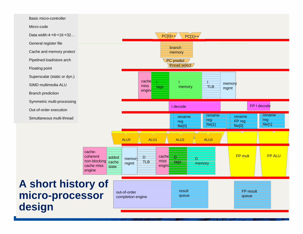
A short history of
memorynon-blockingcache missengine
cache state
memorymgmt TLB missengine
tags
t f d result FP result
Copyright © 2010, Tensilica, Inc.Copyright © 2011, Tensilica, Inc. 8
micro-processor design
out-of-ordercompletion engine
result queue
FP result queue
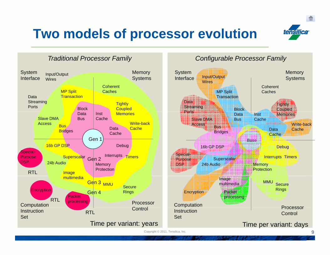
Two models of processor evolutionConfigurable Processor Family
MemorySystems
SystemInterface
Input/OutputWires
Traditional Processor Family
MemorySystems
SystemInterface Input/OutputSystemsInterface
TightlyCoupled
CoherentCaches
Block
MP Split TransactionData
StreamingPorts
Wires SystemsInterface
TightlyCoupled
CoherentCaches
Block
MP Split Transaction
Data StreamingPorts
Wires
Gen 1
InstCache
DataCache
Write-backCache
Memories
Bus Bridges
DataBusSlave DMA
Access
Base
InstCache
DataCache
Write-backCache
pMemories
Bus Bridges
DataBusSlave DMA
Access
Ports
RTL
Interrupts
Debug
Memory Protection
Timers
16b GP DSP
24b Audio
Image
SuperscalarSpecial-PurposeDSP Gen 2 Interrupts
Debug
Memory Protection
Timers
16b GP DSP
24b AudioSuperscalar
Special-PurposeDSP
RTL ProcessorControl
Computation
MMU Secure Rings
multimedia
EncryptionPacketprocessing
Gen 3
Gen 4
ProcessorComputation
MMU Secure RingsEncryption Packet
processing
Imagemultimedia
Copyright © 2010, Tensilica, Inc.Copyright © 2011, Tensilica, Inc. 9
RTLControlInstruction
SetTime per variant: years Time per variant: days
ProcessorControlInstruction
Set
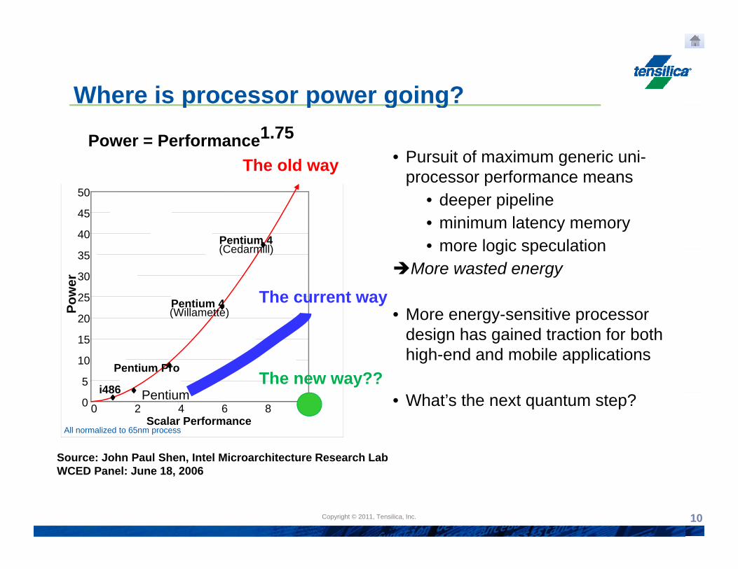
Where is processor power going?p p g g
Power = Performance1.75• Pursuit of maximum generic uni-
processor performance meansThe old way
40
45
50
Pentium 4(Cedarmill)
processor performance means • deeper pipeline• minimum latency memory• more logic speculation
20
25
30
35
Pow
er
Pentium 4(Willamette)
(Cedarmill) more logic speculation More wasted energy
• More energy-sensitive processor The current way
5
10
15
20
i486 P ti
Pentium Pro
gy pdesign has gained traction for both high-end and mobile applications
The new way??
Source: John Paul Shen, Intel Microarchitecture Research Lab
0 0 2 4 6 8 10Scalar Performance
i486 Pentium
All normalized to 65nm process
• What’s the next quantum step?
Copyright © 2010, Tensilica, Inc.Copyright © 2011, Tensilica, Inc. 10
WCED Panel: June 18, 2006
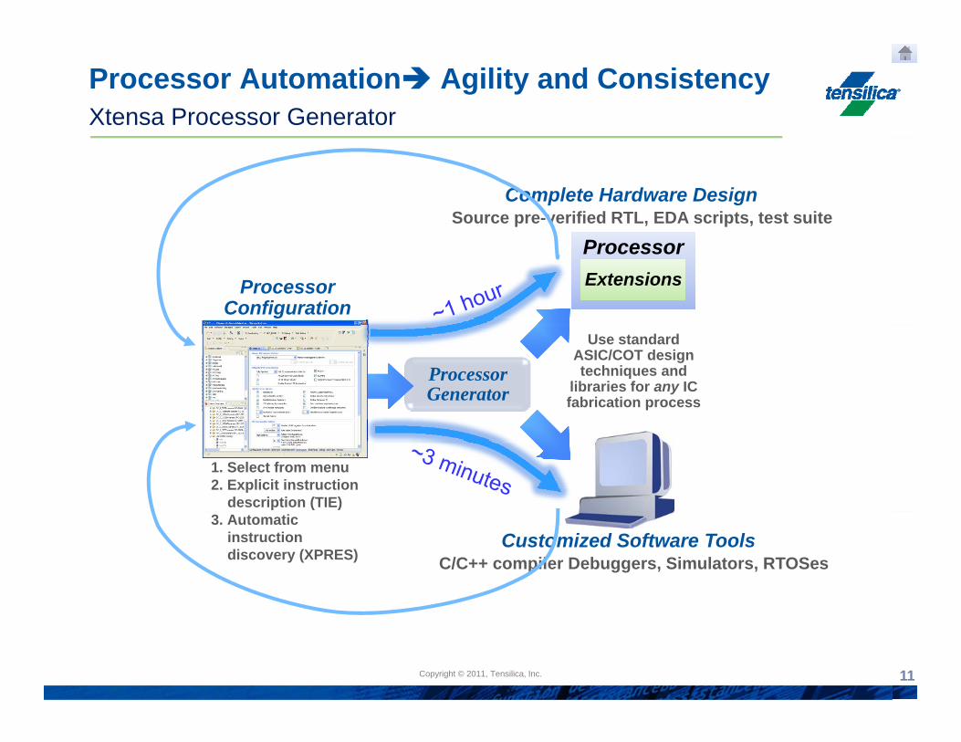
Processor Automation Agility and ConsistencyXtensa Processor Generator
Complete Hardware DesignSource pre-verified RTL, EDA scripts, test suite
Processor Configuration
ProcessorProcessorExtensionsExtensions
ProcessorGenerator
Use standard ASIC/COT design techniques and
libraries for any IC fabrication process
1. Select from menu2. Explicit instruction
description (TIE)
Customized Software ToolsC/C++ compiler Debuggers, Simulators, RTOSes
3. Automatic instruction discovery (XPRES)
Copyright © 2010, Tensilica, Inc.Copyright © 2011, Tensilica, Inc. 11
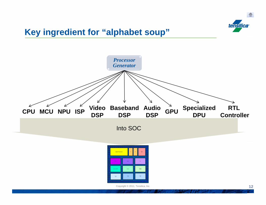
Key ingredient for “alphabet soup”
ProcessorGGenerator
MCU BasebandDSP
VideoDSP
AudioDSPNPU GPUCPU Specialized
DPURTL
ControllerISP DSPDSP DSP DPU Controller
Into SOC
Apps Processor
Audio Video 3D
IO MemCtl
IO
Copyright © 2010, Tensilica, Inc.Copyright © 2011, Tensilica, Inc. 12
Radio1
Radio3
Radio2
Camera Ctl/ISP Security DisplayControl
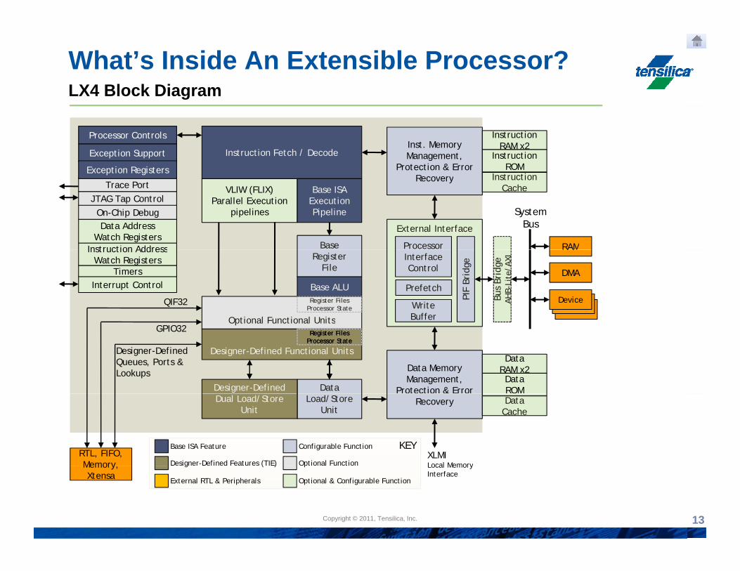
What’s Inside An Extensible Processor?LX4 Block Diagram
Inst. Memory Management,
Protection & Error Recovery
InstructionRAM x2
InstructionROM
Processor Controls
Exception Support
Exception Registers
Instruction Fetch / Decode
InstructionVLIW (FLIX)
Parallel Execution pipelines
Recovery
External Interface
Processor
Trace PortJTAG Tap Control
Data AddressWatch Registers
Instruction Address
On-Chip Debug
Base
Base ISA Execution Pipeline
RAM
SystemBus
InstructionCache
Interface Control
Write Buffer
PIF
Brid
ge
QIF32
Instruction AddressWatch Registers
TimersInterrupt Control
Register File
Base ALU
Optional Functional Units
Register FilesProcessor State Device
Device
Bus
Brid
geAH
B-Li
te/A
XI
RAM
DMA
DevicePrefetch
Data Memory Management,
Protection & Error
DataRAM x2DataROM
GPIO32
Designer-Defined Queues, Ports & Lookups
Data
Optional Functional Units
Designer-Defined
Designer-Defined Functional Units
Register FilesProcessor StateRegister Files
Processor State
Recovery
XLMI Local Memory
Base ISA Feature
Designer-Defined Features (TIE)
Configurable Function
Optional FunctionRTL, FIFO, Memory
KEY
Load/Store Unit
Dual Load/Store Unit
DataCache
Copyright © 2010, Tensilica, Inc.Copyright © 2011, Tensilica, Inc. 13
Local MemoryInterface
g ( )
External RTL & Peripherals
p
Optional & Configurable Function
Memory, Xtensa
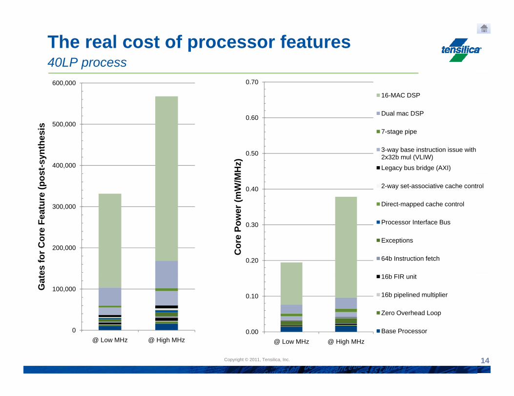
The real cost of processor features 40LP process
500 000
600,000
0.60
0.70
16-MAC DSP
Dual mac DSP
400,000
500,000
st-s
ynth
esis
0.50
Hz)
7-stage pipe
3-way base instruction issue with 2x32b mul (VLIW)Legacy bus bridge (AXI)
300,000
Feat
ure
(pos
0 30
0.40
ower
(mW
/M
2-way set-associative cache control
Direct-mapped cache control
Processor Interface Bus
200,000
es fo
r Cor
e F
0.20
0.30
Cor
e Po
Processor Interface Bus
Exceptions
64b Instruction fetch
100,000Gat
e
0.10
16b FIR unit
16b pipelined multiplier
Zero Overhead Loop
Copyright © 2010, Tensilica, Inc.Copyright © 2011, Tensilica, Inc. 14
0@ Low MHz @ High MHz
0.00@ Low MHz @ High MHz
Base Processor
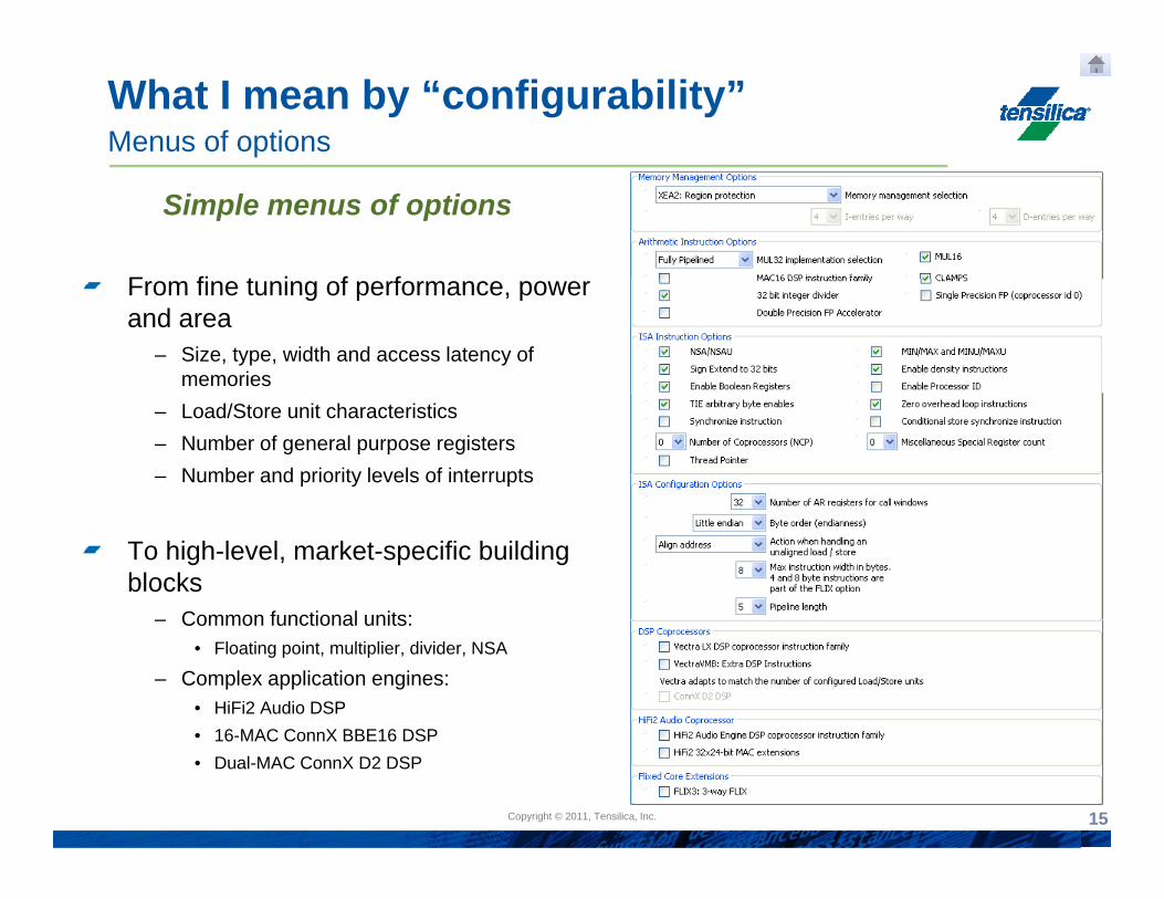
What I mean by “configurability”Menus of options
Simple menus of options
F fi t i f fFrom fine tuning of performance, power and area
– Size, type, width and access latency of memories
– Load/Store unit characteristics– Number of general purpose registers– Number and priority levels of interrupts
To high-level, market-specific building blocks
– Common functional units:– Common functional units: • Floating point, multiplier, divider, NSA
– Complex application engines: • HiFi2 Audio DSP• 16 MAC ConnX BBE16 DSP
Copyright © 2010, Tensilica, Inc.Copyright © 2011, Tensilica, Inc. 15
• 16-MAC ConnX BBE16 DSP• Dual-MAC ConnX D2 DSP
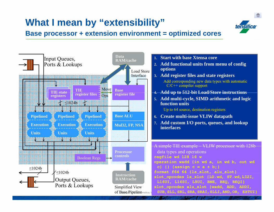
What I mean by “extensibility”Base processor + extension environment = optimized cores
Data RAM/cache 1. Start with base Xtensa core
2. Add functional units from menu of config Input Queues, Ports & Lookups
Base i fi
goptions
3. Add register files and state registers Add corresponding new data types with automatic
C/C++ compiler support
4 Add up to 512-bit Load/Store instructions
Load Store Interface
TIEi fiTIE state
Move
Ports & Lookups
register file
Base ALU
4. Add up to 512-bit Load/Store instructions5. Add multi-cycle, SIMD arithmetic and logic
function unitsUp to 64 source, destination registers
6. Create multi-issue VLIW datapath
≤1024b
register filesTIE state registers Ops
Pipelined Pipelined Pipelined 7. Add custom I/O ports, queues, and lookup
interfacesExecution
Units
Execution
Units
Execution
Units
Mul32, FP, NSA
A simple TIE example VLIW processor with 128bProcessorcontrolsBoolean Regs
≤1024b≤1024b
A simple TIE example – VLIW processor with 128b data types and operations
regfile wd 128 16 woperation wadd {in wd a, in wd b, out wd c} {} {assign c = a + b;}
format f64 64 {ls slot, alu slot}
Copyright © 2010, Tensilica, Inc.Copyright © 2011, Tensilica, Inc. 16
Instruction RAM/cache
Simplified View of Base Pipeline
Output Queues, Ports & Lookups
≤1024b format f64 64 {ls_slot, alu_slot}slot_opcodes ls_slot {LD.wd, ST.wd,L32I, L16UI, L16SI, L8UI, BNE, BEQ, BEQI}
slot_opcodes alu_slot {wadd, ADD, ADDI, SUB,SLL,SRL,SRA,SRAI,SLLI,AND,OR, EXTUI}
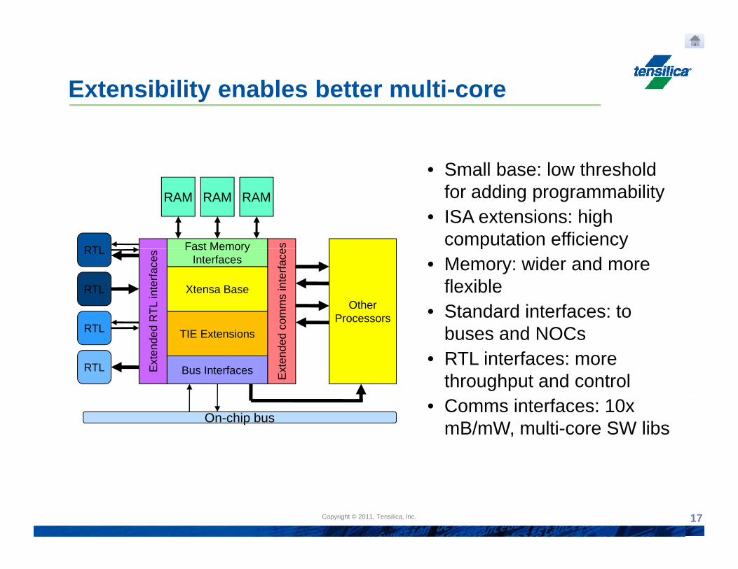
Extensibility enables better multi-core
• Small base: low threshold
Fast Memory esRTL
RAM RAM RAM for adding programmability• ISA extensions: high
computation efficiency
Xtensa Base
Fast Memory Interfaces
RTL
inte
rface
s
omm
s in
terfa
ceRTL
RTLOther
Processors
p y• Memory: wider and more
flexible• Standard interfaces: to
TIE Extensions
Bus InterfacesExt
ende
d R
Ext
ende
d co
RTL
RTLProcessors
buses and NOCs• RTL interfaces: more
throughput and control
On-chip bus• Comms interfaces: 10x
mB/mW, multi-core SW libs
Copyright © 2010, Tensilica, Inc.Copyright © 2011, Tensilica, Inc. 17
Pushing the envelope on small• What happens if you really pare
down the processor to essentials• General-purpose 32b ISA
Small cores: Power and Area45gs Synthesis
• General-purpose 32b ISA• Fast 5-stage pipeline• Local instruction/data memories• Optional bus interface, interrupts and
0.02
)
Pico ( to 1.2GHz)
Femto (to 1.4GHz)
exception handling, multiply/divide, zero-overhead loops
• Example Footprint (45gs): C 0.01
0.015
er (m
W/M
Hz)
• Core+ Byte-wide serial boot-loader+ 2KB/2KB memory [yes, tiny]• 0.052mm2 to 0.072mm2 floorplan area
0.005C
ore
Pow
e0.052mm to 0.072mm floorplan area
• up to ~20 cores/mm2
• up to ~25,000 DMIPS/mm2
• Extrapolate to 22nm process:
00 10,000 20,000 30,000 40,000
Post Layout Cell Area (μ2)
Copyright © 2010, Tensilica, Inc.Copyright © 2011, Tensilica, Inc. 18
p p• ~80 cores/mm2
• > 120,000 DMIPS/mm2
Post Layout Cell Area (μ )
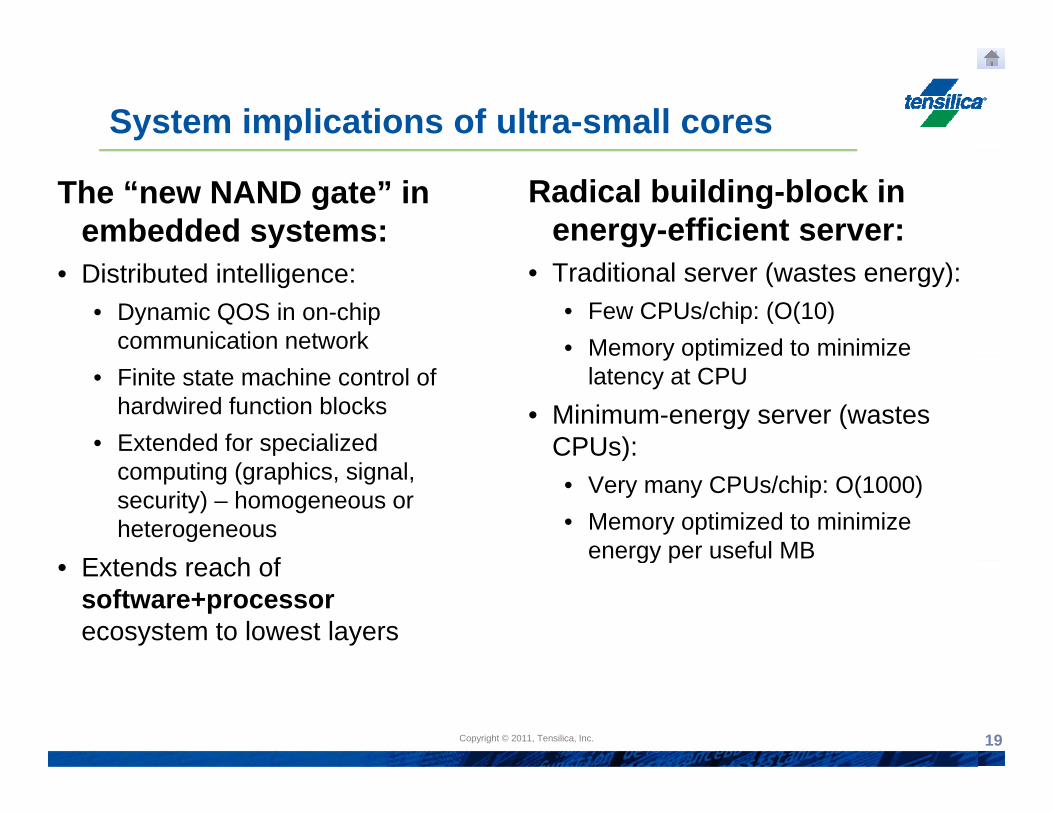
System implications of ultra-small cores
The “new NAND gate” in embedded systems:
Radical building-block in energy-efficient server:
• Distributed intelligence:• Dynamic QOS in on-chip
communication network
• Traditional server (wastes energy):• Few CPUs/chip: (O(10)• Memory optimized to minimize
• Finite state machine control of hardwired function blocks
• Extended for specialized
Memory optimized to minimize latency at CPU
• Minimum-energy server (wastes CPUs):
computing (graphics, signal, security) – homogeneous or heterogeneous
E t d h f
)• Very many CPUs/chip: O(1000)• Memory optimized to minimize
energy per useful MB• Extends reach of
software+processor ecosystem to lowest layers
gy p
Copyright © 2010, Tensilica, Inc.Copyright © 2011, Tensilica, Inc. 19
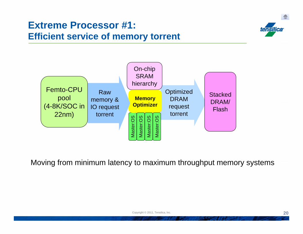
Extreme Processor #1:Efficient service of memory torrent
On-chip
OptimizedDRAM
SRAMhierarchy
MemoryRaw
memory & Femto-CPU
pool StackedDRAM/
request torrent
aste
r:OS
Optimizer
aste
r:OS
aste
r:OS
aste
r:OS
yIO request
torrent(4-8K/SOC in
22nm)
DRAM/ Flash
Ma
Ma
Ma
Ma
Moving from minimum latency to maximum throughput memory systemsMoving from minimum latency to maximum throughput memory systems
Copyright © 2010, Tensilica, Inc.Copyright © 2011, Tensilica, Inc. 20
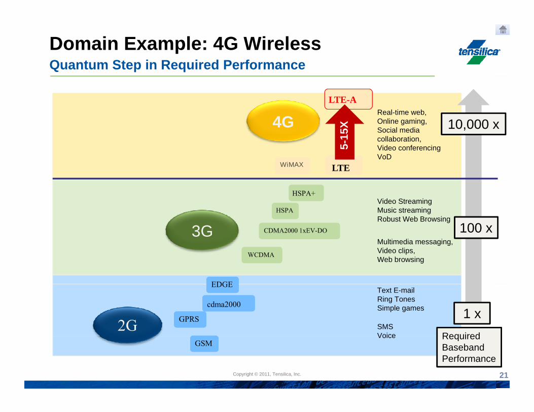
Domain Example: 4G WirelessQuantum Step in Required Performance
Real-time web, Online gaming, S i l di
4GLTE-A
10,000 xX Social media collaboration,Video conferencingVoD
WiMAX LTE
10,000 x
5-15
X
3G
Video StreamingMusic streamingRobust Web Browsing
CDMA2000 1xEV-DO
HSPA
HSPA+
100 x3GMultimedia messaging, Video clips,Web browsing
EDGE
WCDMA
CDMA2000 1xEV DO 100 x
2G
Text E-mailRing TonesSimple games
SMSVoice Required
GPRS
cdma2000
EDGE
1 x
Copyright © 2010, Tensilica, Inc.Copyright © 2011, Tensilica, Inc. 21
Voice RequiredBaseband Performance
GSM
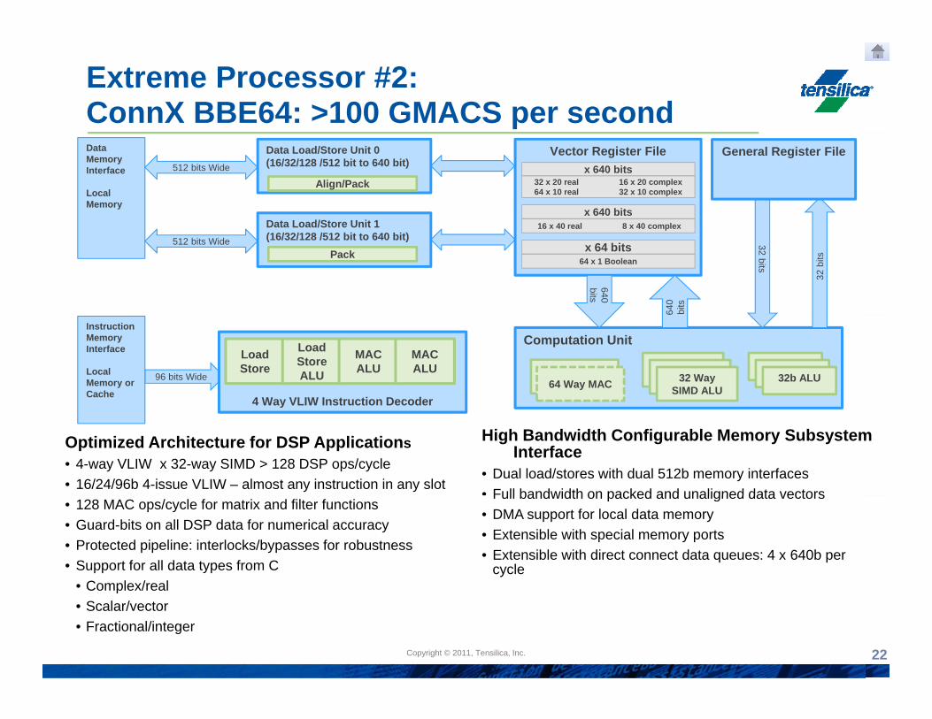
Extreme Processor #2:ConnX BBE64: >100 GMACS per secondData Memory Interface
Local Memory
512 bits Widex 32 bits
Data Load/Store Unit 0(16/32/128 /512 bit to 640 bit)
Data Load/Store Unit 1
Vector Register Filex 640 bits
32 x 20 real 16 x 20 complex64 x 10 real 32 x 10 complex
x 640 bits 16 40 l 8 40 l
Align/Pack
General Register File
512 bits Wide
Data Load/Store Unit 1(16/32/128 /512 bit to 640 bit)
16 x 40 real 8 x 40 complex
x 64 bits 64 x 1 Boolean
Pack
640
bits
32 bits
32 b
its
640 bits
96 bits Wide
4 Way VLIW Instruction Decoder
LoadStore
Instruction Memory Interface
Local Memory or Cache
Computation Unit
32b ALU64 Way MAC
32 Way SIMD ALU32 Way
SIMD ALU32 Way SIMD ALU64 Way MAC
LoadStoreALU
MACALU
MACALU
6
32b ALU32b ALU
Optimized Architecture for DSP Applications• 4-way VLIW x 32-way SIMD > 128 DSP ops/cycle• 16/24/96b 4-issue VLIW – almost any instruction in any slot
High Bandwidth Configurable Memory Subsystem Interface
• Dual load/stores with dual 512b memory interfaces • Full bandwidth on packed and unaligned data vectors
4 Way VLIW Instruction Decoder
• 128 MAC ops/cycle for matrix and filter functions• Guard-bits on all DSP data for numerical accuracy• Protected pipeline: interlocks/bypasses for robustness• Support for all data types from C
• Complex/real
Full bandwidth on packed and unaligned data vectors• DMA support for local data memory• Extensible with special memory ports• Extensible with direct connect data queues: 4 x 640b per
cycle
Copyright © 2010, Tensilica, Inc.Copyright © 2011, Tensilica, Inc. 22
• Complex/real• Scalar/vector• Fractional/integer
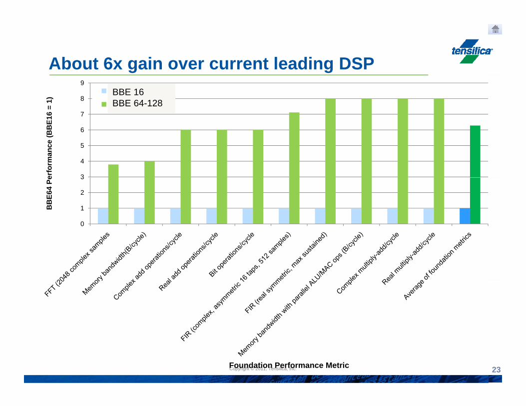
About 6x gain over current leading DSP
7
8
9
BE1
6 =
1)
BBE16BBE64+BBE 16BBE 64-128
3
4
5
6
erfo
rman
ce (B
B
0
1
2
3
BB
E64
Pe
Copyright © 2010, Tensilica, Inc.Copyright © 2011, Tensilica, Inc. 23Foundation Performance Metric
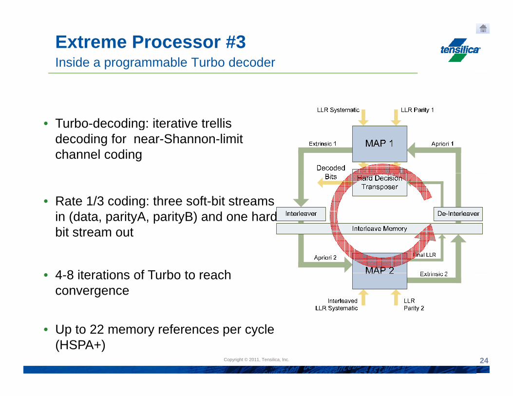
Extreme Processor #3Inside a programmable Turbo decoder
• Turbo decoding: iterative trellis• Turbo-decoding: iterative trellis decoding for near-Shannon-limit channel coding
• Rate 1/3 coding: three soft-bit streams in (data, parityA, parityB) and one hard-( p y p y )bit stream out
4 8 iterations of Turbo to reach• 4-8 iterations of Turbo to reach convergence
Copyright © 2010, Tensilica, Inc.Copyright © 2011, Tensilica, Inc. 24
• Up to 22 memory references per cycle (HSPA+)
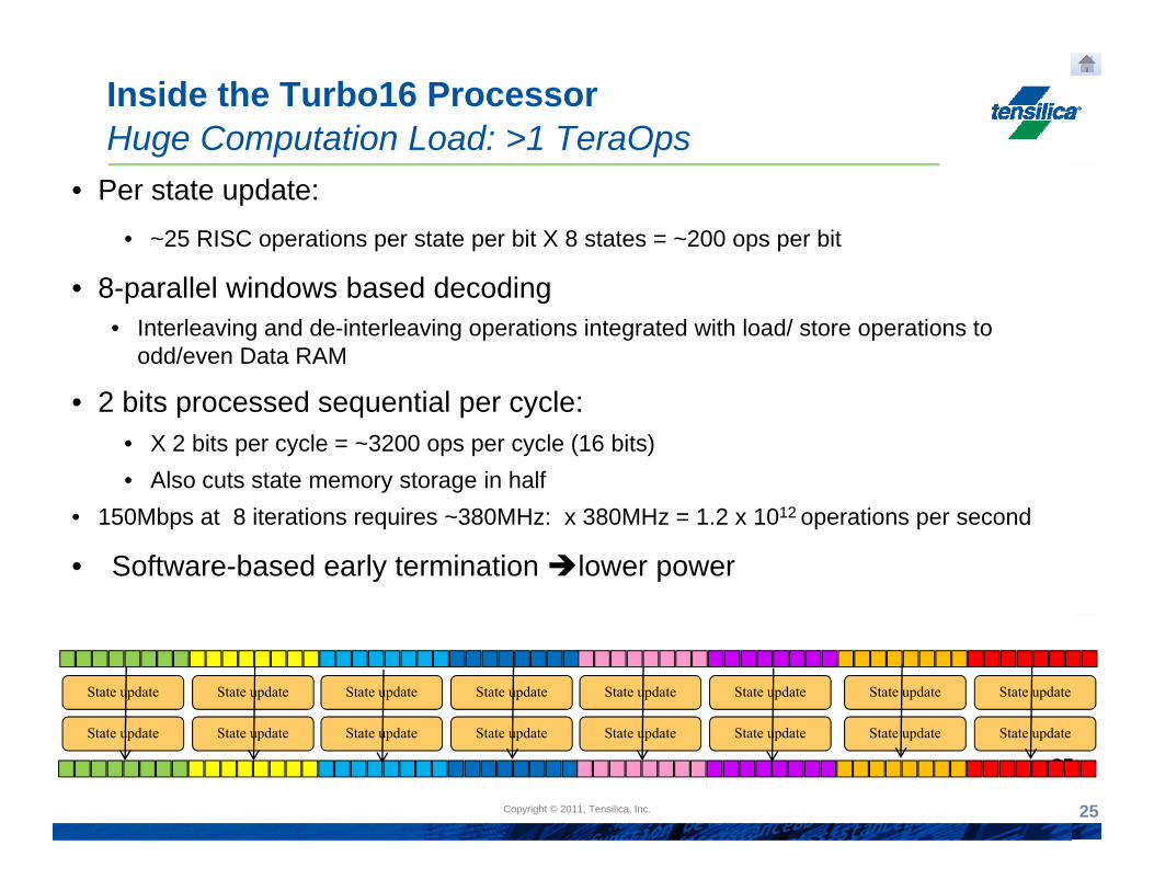
Inside the Turbo16 ProcessorHuge Computation Load: >1 TeraOps
• Per state update:• ~25 RISC operations per state per bit X 8 states = ~200 ops per bit
8 ll l i d b d d di• 8-parallel windows based decoding• Interleaving and de-interleaving operations integrated with load/ store operations to
odd/even Data RAM
• 2 bits processed sequential per cycle: • X 2 bits per cycle = ~3200 ops per cycle (16 bits)• Also cuts state memory storage in half
• 150Mbps at 8 iterations requires ~380MHz: x 380MHz = 1.2 x 10¹² operations per second
• Software-based early termination lower power
State update State update State update State update State update State update State update State update
Copyright © 2010, Tensilica, Inc.Copyright © 2011, Tensilica, Inc. 25
25State update State update State update State update State update State update State update State update
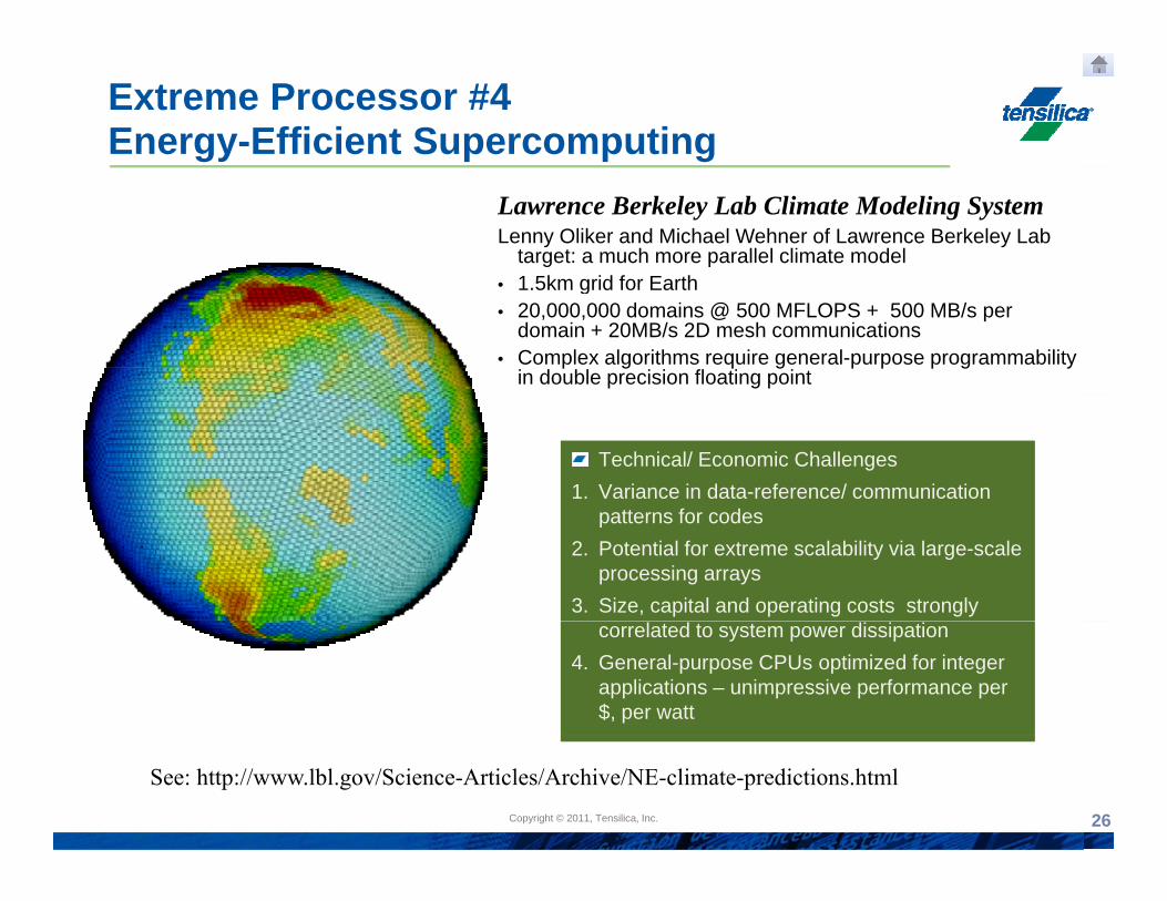
Extreme Processor #4Energy-Efficient Supercomputing
Lawrence Berkeley Lab Climate Modeling System Lenny Oliker and Michael Wehner of Lawrence Berkeley Lab
target: a much more parallel climate model1 5km grid for Earth• 1.5km grid for Earth
• 20,000,000 domains @ 500 MFLOPS + 500 MB/s per domain + 20MB/s 2D mesh communications
• Complex algorithms require general-purpose programmability in double precision floating point
Technical/ Economic Challenges1. Variance in data-reference/ communication
Technical/ Economic Challenges1. Variance in data-reference/ communication
patterns for codes2. Potential for extreme scalability via large-scale
processing arrays3. Size, capital and operating costs strongly
patterns for codes2. Potential for extreme scalability via large-scale
processing arrays3. Size, capital and operating costs strongly
correlated to system power dissipation4. General-purpose CPUs optimized for integer
applications – unimpressive performance per $, per watt
correlated to system power dissipation4. General-purpose CPUs optimized for integer
applications – unimpressive performance per $, per watt
Copyright © 2010, Tensilica, Inc.Copyright © 2011, Tensilica, Inc. 26
See: http://www.lbl.gov/Science-Articles/Archive/NE-climate-predictions.html
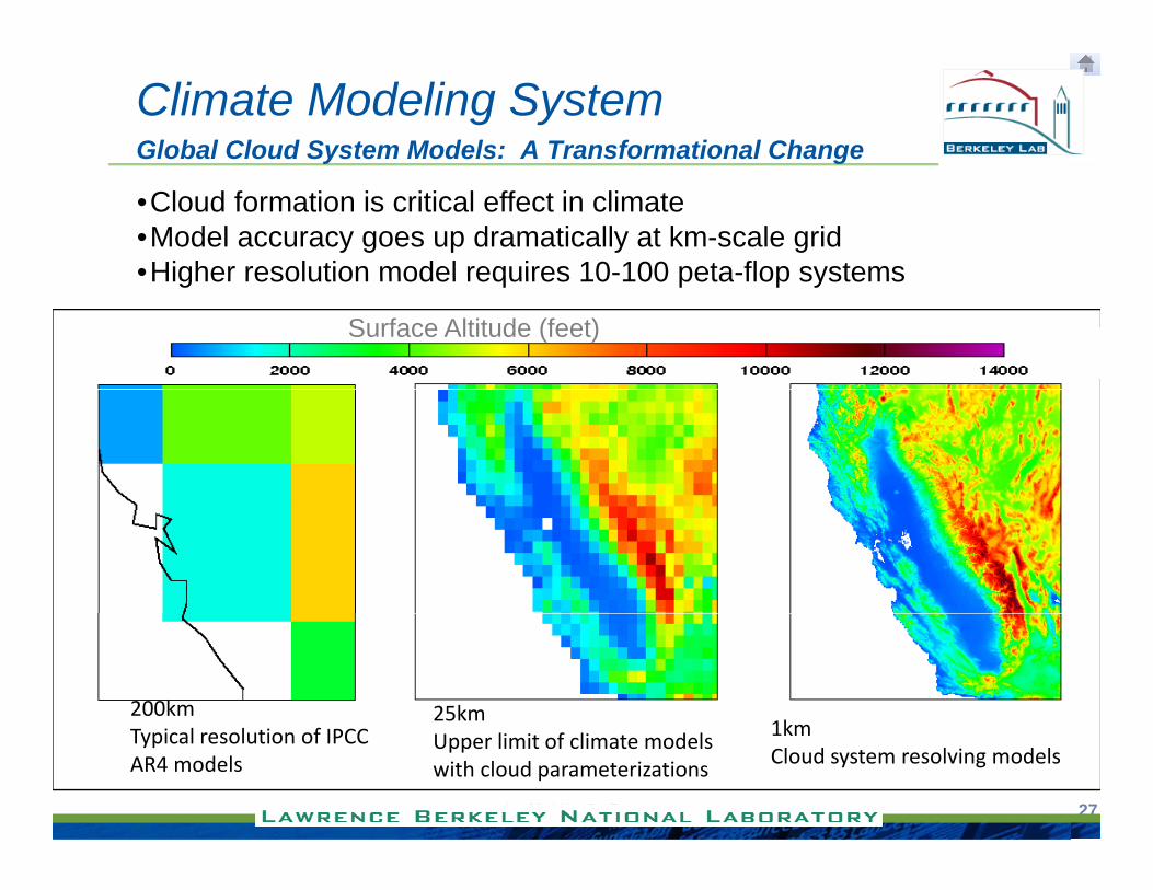
Climate Modeling SystemGlobal Cloud System Models: A Transformational Change
•Cloud formation is critical effect in climate•Model accuracy goes up dramatically at km-scale grid•Higher resolution model requires 10-100 peta-flop systems
Surface Altitude (feet)
Higher resolution model requires 10 100 peta flop systems
1km25km200km
Copyright © 2010, Tensilica, Inc.Copyright © 2011, Tensilica, Inc. 27
1kmCloud system resolving models
Upper limit of climate models with cloud parameterizations
Typical resolution of IPCC AR4 models
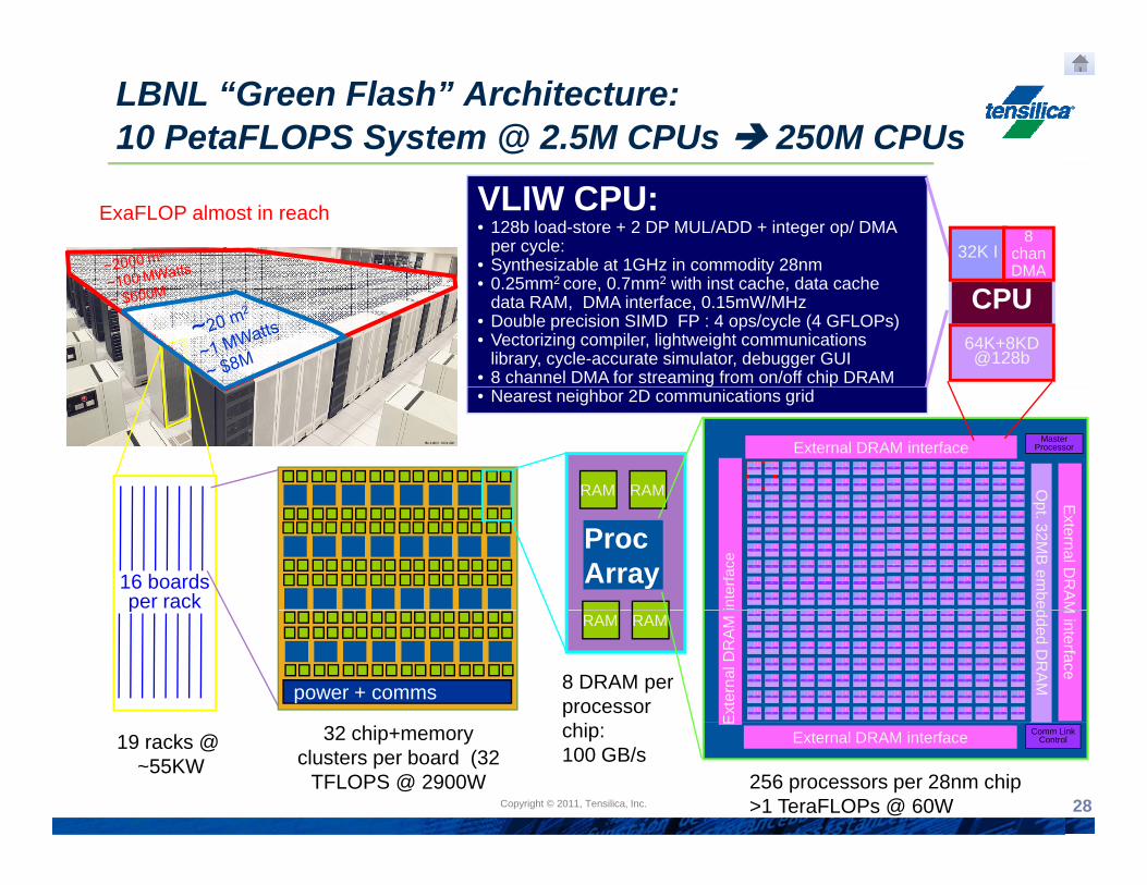
LBNL “Green Flash” Architecture: 10 PetaFLOPS System @ 2.5M CPUs 250M CPUs
VLIW CPU: • 128b load-store + 2 DP MUL/ADD + integer op/ DMA
per cycle:• Synthesizable at 1GHz in commodity 28nm
ExaFLOP almost in reach
32K I8
chanDMA
• 0.25mm2 core, 0.7mm2 with inst cache, data cache data RAM, DMA interface, 0.15mW/MHz
• Double precision SIMD FP : 4 ops/cycle (4 GFLOPs)• Vectorizing compiler, lightweight communications
library, cycle-accurate simulator, debugger GUI• 8 channel DMA for streaming from on/off chip DRAM
CPUDMA
64K+8KD@128b
• Nearest neighbor 2D communications grid
RAM RAM O
External DRAM interfaceMaster
Processor
CPU
D
IDM A
CPU
D
IDM A
CPU
D
IDM A
CPU
D
IDM A
CPU
D
IDM A
CPU
D
IDM A
CPU
D
IDM A
CPU
D
IDM A
CPU
D
IDM A
CPU
D
IDM A
CPU
D
IDM A
CPU
D
IDM A
CPU
D
IDM A
CPU
D
IDM A
CPU
D
IDM A
CPU
D
IDM A
IDM A
IDM A
IDM A
IDM A
IDM A
IDM A
IDM A
IDM A
CPU
D
IDM A
CPU
D
IDM A
CPU
D
IDM A
CPU
D
IDM A
CPU
D
IDM A
CPU
D
IDM A
CPU
D
IDM A
CPU
D
IDM A
CPU
D
IDM A
CPU
D
IDM A
CPU
D
IDM A
CPU
D
IDM A
CPU
D
IDM A
CPU
D
IDM A
CPU
D
IDM A
CPU
D
IDM A
IDM A
IDM A
IDM A
IDM A
IDM A
IDM A
IDM A
IDM A
16 boards per rack
ProcArray
Opt. 32M
B em
bed
External D
RA
Minte
rface
CPU
D
CPU
D
CPU
D
CPU
D
CPU
D
CPU
D
CPU
D
CPU
D
CPU
D
IDM A
CPU
D
IDM A
CPU
D
IDM A
CPU
D
IDM A
CPU
D
IDM A
CPU
D
IDM A
CPU
D
IDM A
CPU
D
IDM A
CPU
D
IDM A
CPU
D
IDM A
CPU
D
IDM A
CPU
D
IDM A
CPU
D
IDM A
CPU
D
IDM A
CPU
D
IDM A
CPU
D
IDM A
CPU
D
IDM A
CPU
D
IDM A
CPU
D
IDM A
CPU
D
IDM A
CPU
D
IDM A
CPU
D
IDM A
CPU
D
IDM A
CPU
D
IDM A
CPU
D
IDM A
CPU
D
IDM A
CPU
D
IDM A
CPU
D
IDM A
CPU
D
IDM A
CPU
D
IDM A
CPU
D
IDM A
CPU
D
IDM A
CPU
D
IDM A
CPU
D
IDM A
CPU
D
IDM A
CPU
D
IDM A
CPU
D
IDM A
CPU
D
IDM A
CPU
D
IDM A
CPU
D
IDM A
CPU
D
CPU
D
CPU
D
CPU
D
CPU
D
CPU
D
CPU
D
CPU
D
CPU
D
IDM A
CPU
D
IDM A
CPU
D
IDM A
CPU
D
IDM A
CPU
D
IDM A
CPU
D
IDM A
CPU
D
IDM A
CPU
D
IDM A
CPU
D
IDM A
CPU
D
IDM A
CPU
D
IDM A
CPU
D
IDM A
CPU
D
IDM A
CPU
D
IDM A
CPU
D
IDM A
CPU
D
IDM A
CPU
D
IDM A
CPU
D
IDM A
CPU
D
IDM A
CPU
D
IDM A
CPU
D
IDM A
CPU
D
IDM A
CPU
D
IDM A
CPU
D
IDM A
CPU
D
IDM A
CPU
D
IDM A
CPU
D
IDM A
CPU
D
IDM A
CPU
D
IDM A
CPU
D
IDM A
CPU
D
IDM A
CPU
D
IDM A
CPU
D
IDM A
CPU
D
IDM A
CPU
D
IDM A
CPU
D
IDM A
CPU
D
IDM A
CPU
D
IDM A
CPU
D
IDM A
CPU
D
IDM A
CPU
D
IDM A
CPU
D
IDM A
CPU
D
IDM A
CPU
D
IDM A
CPU
D
IDM A
CPU
D
IDM A
CPU
D
IDM A
CPU
D
IDM A
D D D D D D D D
CPU
D
IDM A
CPU
D
IDM A
CPU
D
IDM A
CPU
D
IDM A
CPU
D
IDM A
CPU
D
IDM A
CPU
D
IDM A
CPU
D
IDM A
D D D D D D D Dp
power + comms
RAM RAM
8 DRAM perprocessor
dded DR
AM
M interface
Ext
erna
l DR
AM
CPU
D
I M A
CPU
D
I M A
CPU
D
I M A
CPU
D
I M A
CPU
D
I M A
CPU
D
I M A
CPU
D
I M A
CPU
D
I M A
CPU
D
IDM A
CPU
D
IDM A
CPU
D
IDM A
CPU
D
IDM A
CPU
D
IDM A
CPU
D
IDM A
CPU
D
IDM A
CPU
D
IDM A
CPU
D
IDM A
CPU
D
IDM A
CPU
D
IDM A
CPU
D
IDM A
CPU
D
IDM A
CPU
D
IDM A
CPU
D
IDM A
CPU
D
IDM A
CPU
D
IDM A
CPU
D
IDM A
CPU
D
IDM A
CPU
D
IDM A
CPU
D
IDM A
CPU
D
IDM A
CPU
D
IDM A
CPU
D
IDM A
CPU
D
IDM A
CPU
D
IDM A
CPU
D
IDM A
CPU
D
IDM A
CPU
D
IDM A
CPU
D
IDM A
CPU
D
IDM A
CPU
D
IDM A
CPU
D
IDM A
CPU
D
IDM A
CPU
D
IDM A
CPU
D
IDM A
CPU
D
IDM A
CPU
D
IDM A
CPU
D
IDM A
CPU
D
IDM A
CPU
D
IDM A
CPU
D
IDM A
CPU
D
IDM A
CPU
D
IDM A
CPU
D
IDM A
CPU
D
IDM A
CPU
D
IDM A
CPU
D
IDM A
CPU
D
I M A
CPU
D
I M A
CPU
D
I M A
CPU
D
I M A
CPU
D
I M A
CPU
D
I M A
CPU
D
I M A
CPU
D
I M A
CPU
D
IDM A
CPU
D
IDM A
CPU
D
IDM A
CPU
D
IDM A
CPU
D
IDM A
CPU
D
IDM A
CPU
D
IDM A
CPU
D
IDM A
CPU
D
IDM A
CPU
D
IDM A
CPU
D
IDM A
CPU
D
IDM A
CPU
D
IDM A
CPU
D
IDM A
CPU
D
IDM A
CPU
D
IDM A
CPU
D
IDM A
CPU
D
IDM A
CPU
D
IDM A
CPU
D
IDM A
CPU
D
IDM A
CPU
D
IDM A
CPU
D
IDM A
CPU
D
IDM A
CPU
D
IDM A
CPU
D
IDM A
CPU
D
IDM A
CPU
D
IDM A
CPU
D
IDM A
CPU
D
IDM A
CPU
D
IDM A
CPU
D
IDM A
CPU
D
IDM A
CPU
D
IDM A
CPU
D
IDM A
CPU
D
IDM A
CPU
D
IDM A
CPU
D
IDM A
CPU
D
IDM A
CPU
D
IDM A
CPU
D
IDM A
CPU
D
IDM A
CPU
D
IDM A
CPU
D
IDM A
CPU
D
IDM A
CPU
D
IDM A
CPU
D
IDM A
CPU
D
IDM A
Copyright © 2010, Tensilica, Inc.Copyright © 2011, Tensilica, Inc. 28
19 racks @ ~55KW
32 chip+memoryclusters per board (32
TFLOPS @ 2900W
chip: 100 GB/s
External DRAM interfaceE
Comm LinkControl
256 processors per 28nm chip>1 TeraFLOPs @ 60W
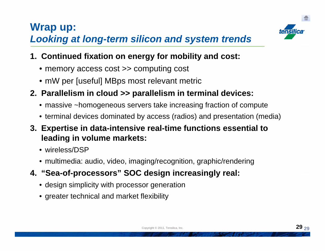
Wrap up: Looking at long-term silicon and system trends1. Continued fixation on energy for mobility and cost:
• memory access cost >> computing costW [ f l] MB t l t t i• mW per [useful] MBps most relevant metric
2. Parallelism in cloud >> parallelism in terminal devices:• massive ~homogeneous servers take increasing fraction of compute• terminal devices dominated by access (radios) and presentation (media)
3. Expertise in data-intensive real-time functions essential to leading in volume markets:g• wireless/DSP• multimedia: audio, video, imaging/recognition, graphic/rendering
4 “Sea-of-processors” SOC design increasingly real:4. Sea-of-processors SOC design increasingly real:• design simplicity with processor generation• greater technical and market flexibility
Copyright © 2010, Tensilica, Inc.Copyright © 2011, Tensilica, Inc. 2929
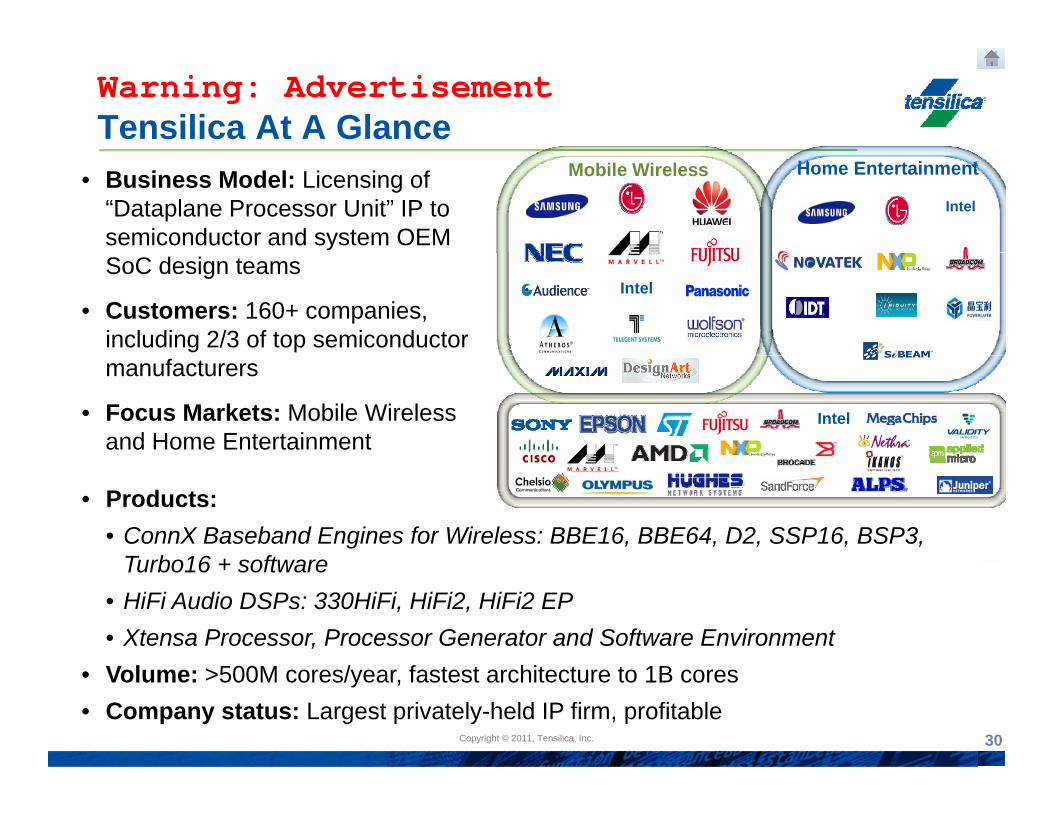
Warning: AdvertisementTensilica At A Glance
• Business Model: Licensing of “Dataplane Processor Unit” IP to semiconductor and system OEM
Mobile Wireless Home Entertainment
Intel
SoC design teams
• Customers: 160+ companies, including 2/3 of top semiconductor
Intel
manufacturers
• Focus Markets: Mobile Wireless and Home Entertainment
Intel
• Products: • ConnX Baseband Engines for Wireless: BBE16, BBE64, D2, SSP16, BSP3,
Turbo16 + softwareTurbo16 + software• HiFi Audio DSPs: 330HiFi, HiFi2, HiFi2 EP• Xtensa Processor, Processor Generator and Software Environment
Copyright © 2010, Tensilica, Inc.Copyright © 2011, Tensilica, Inc. 30
• Volume: >500M cores/year, fastest architecture to 1B cores• Company status: Largest privately-held IP firm, profitable