smarresearch fieldbus communications controller … · training custom design smarresearch ... •...
TRANSCRIPT
©Smar Research Corporation 1 FB3050AppNotes - 0303
HART®
Fieldbus Profibus Intrinsic Safety Configuration Tools Semiconductors Training Custom Design
SmarResearch TechnologySource
Featured Topics • Detailed Discussion of Typical FB3050 Design and Interface • Reference Design Using Motorola HC11 and External RAM and ROM • Clocks • Microcontroller Interfacing • Memory Interfacing and Mapping • Cycle Sharing and Timing • Medium Attachment Unit (MAU) Analog Interfacing • Software Procedures • And More....
Fieldbus Communications Controller
FB3050 Application Note
Visit the SmarResearch technology center at: www.smarresearch.com

©Smar Research Corporation 2 FB3050AppNotes - 0303
FB
30
50
Ge
ne
ral D
esc
rip
tio
n
General Description
The purpose of this document is to detail an example of a typical design using the FB3050. This reference design will provide greater understanding as to how the FB3050 interfaces and functions using a Motorola HC11 and external memory. While a Motorola microcontroller is used in this example, the FB3050 can also be used with microcontrollers and microprocessors from most major vendors such as Intel, Hitachi and NEC. To fully understand the FB3050 and its many functions, this guide should be used in conjunction with the FB3050 Datasheet that can be found on the Smar Research website: http://www.SmarResearch.com.
The reference design explained in this application note was selected to showcase
a typical design using the FB3050. The reference design will use a FB3050, Motorola HC11 in expanded (multiplexed) mode, 1Mx8 of RAM and 512Kx8 of ROM. While specific needs and medium requirements will vary between actual applications, the concepts and strategies described here cover the basic concepts necessary to implement control system design based on the FB3050. In the pages to follow, specific interconnection, memory mapping and timing diagrams are included and explained.
In order to overcome the 64K memory map limitation of the HC11 the FB3050
utilizes extended (paged) memory mapping. In this way, the FB3050 can effectively address up to 2MB for RAM and 4MB for ROM using the extended address bits PO_XADDR_[7:0]. The FB3050 also provides its own memory mapped chip select signals. The memory map and chip select signals will be discussed in greater detail in the following pages. It should be noted that the FB3050 can also be used by microprocessors with a non multiplexed bus. As can be seen on the pinout in the FB3050 Datasheet, the FB3050 provides input pins for a 16-bit address bus as well as 8 bi-directional pins for an 8-bit data bus.
The FB3050 Fieldbus Interface and Controller conforms to the IEC 61158-2 standard, Fieldbus Physical Layer Definition. Thus, all Fieldbus interconnections from the FB3050 through the Medium Attachment Unit to the Fieldbus network are standard. A generic sample analog interface is provided for reference. The design of a Fieldbus node using the FB3050 will be separated into six topics. The following topics will be discussed including reference examples whenever applicable:
• Clocks • Microcontroller Interfacing • Memory Interfacing and Mapping • Cycle Sharing and Timing • Medium Attachment Unit (MAU) Analog Interface • Software Procedures
©Smar Research Corporation 3 FB3050AppNotes - 0303
FB
30
50
Clo
cks Clocks
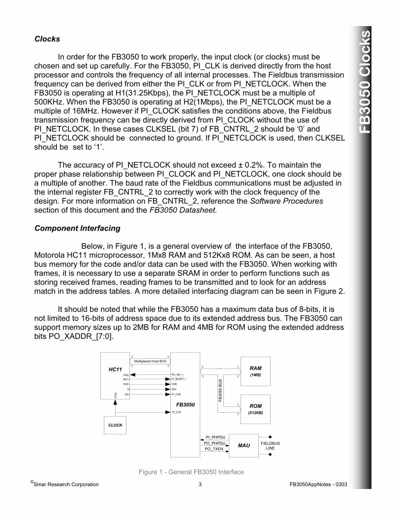
In order for the FB3050 to work properly, the input clock (or clocks) must be chosen and set up carefully. For the FB3050, PI_CLK is derived directly from the host processor and controls the frequency of all internal processes. The Fieldbus transmission frequency can be derived from either the PI_CLK or from PI_NETCLOCK. When the FB3050 is operating at H1(31.25Kbps), the PI_NETCLOCK must be a multiple of 500KHz. When the FB3050 is operating at H2(1Mbps), the PI_NETCLOCK must be a multiple of 16MHz. However if PI_CLOCK satisfies the conditions above, the Fieldbus transmission frequency can be directly derived from PI_CLOCK without the use of PI_NETCLOCK. In these cases CLKSEL (bit 7) of FB_CNTRL_2 should be ‘0’ and PI_NETCLOCK should be connected to ground. If PI_NETCLOCK is used, then CLKSEL should be set to ‘1’. The accuracy of PI_NETCLOCK should not exceed ± 0.2%. To maintain the proper phase relationship between PI_CLOCK and PI_NETCLOCK, one clock should be a multiple of another. The baud rate of the Fieldbus communications must be adjusted in the internal register FB_CNTRL_2 to correctly work with the clock frequency of the design. For more information on FB_CNTRL_2, reference the Software Procedures section of this document and the FB3050 Datasheet. Component Interfacing Below, in Figure 1, is a general overview of the interface of the FB3050, Motorola HC11 microprocessor, 1Mx8 RAM and 512Kx8 ROM. As can be seen, a host bus memory for the code and/or data can be used with the FB3050. When working with frames, it is necessary to use a separate SRAM in order to perform functions such as storing received frames, reading frames to be transmitted and to look for an address match in the address tables. A more detailed interfacing diagram can be seen in Figure 2. It should be noted that while the FB3050 has a maximum data bus of 8-bits, it is not limited to 16-bits of address space due to its extended address bus. The FB3050 can support memory sizes up to 2MB for RAM and 4MB for ROM using the extended address bits PO_XADDR_[7:0].
Figure 1 - General FB3050 Interface
HC11 RAM(1MB)
Multiplexed Host BUS
FB3050
CLOCK
MAUPO_PHPDUPI_PHPDU
PO_TXENFIELDBUS
LINE
FB30
50 B
US
ROM(512KB)
PI_RESET_IPO_INT_I
WR/
RD/
PI_CAS
PI_CLK
XTAL
IRQ/RST/
R/W
E
AS/

©Smar Research Corporation 4 FB3050AppNotes - 0303
FB
30
50
- M
icro
co
ntr
olle
r In
terf
ac
ing
Microcontroller Interfacing The HC11 should be configured internally into extended (multiplexed) mode. In this mode the HC11 will multiplex the lower 8 address bits with the 8 data bits. It should be noted that the 8 multiplexed address/data bits should be connected to PB_CDATA_[7:0] and not PI_ADDR_[7:0] because of their multiplexed nature. Figure 2 shows a detailed interface diagram with the Motorola HC11 using separate memory for code (ROM) and data (RAM). Note that the memory is being shared between the HC11 and the FB3050. A detailed discussion of shared memory and timing diagrams can be found in Cycle Sharing and Timing of this document. For more information on the configuration of the HC11 and extended mode, please refer to the Motorola semiconductor web site http://e-www.motorola.com. In addition to the address/data bus, an interface between the FB3050 and HC11 requires signals to control read/write, address latching, interrupt requests, reset, among others. These signals can be seen in Figure 2 as well as summarized below: • PI_RESET_I must be connected to RST/ of the HC11 for proper reset control • PO_INT_I should be connected to IRQ/ of the HC11 if interrupt handling is desired • WR/ must be connected to R/W of the HC11 for proper bus control • RD/ must be connected to E of the HC11 for proper bus allocation • PI_CAS must be connected to AS/ of the HC11 to ensure proper address latching • PI_CLK must be connected to XTAL of the HC11 for proper clocking The FB3050 has input pins that must be configured to match the operation of the HC11 and the supporting circuitry. The configuration of these signals can be seen in Figure 2 as well as summarized below: • PI_INT_I is an active low signal that should be tied to VCC if not in use • PI_MUX_ON must be tied to VCC because the HC11 bus is multiplexed • PI_EDGE must be tied to VCC to match the rising edge operation of the HC11 • PI_MODE must be tied to GND for proper use with the HC11. • PI_CSMEM_I must be tied to GND to properly use extended addressing • PI_NETCLOCK should be tied to ground unless using an external Fieldbus clock • PI_CSREG_I and PO_MCSF_I should be tied together to allow the FB3050 to enable
its own internal registers. This is required because the HC11 has no dedicated chip select signals.

©Smar Research Corporation 5 FB3050AppNotes - 0303
Figure 2 - FB3050 Component Interconnection
FB
30
50
- C
om
po
ne
nt
Inte
rfa
cin
g
83
82
81
80
79
78
77
94
95
96
97
98
99
3
4
5
6
7
8
9
10
15
16
17
18
PB_MDATA_0
FB3050
19
20
21
22
27
28
39
42
41
40
PO_MADDR_15
PO_MADDR_13
PO_MADDR_14
PO_MADDR_11
PO_MADDR_12
PO_MADDR_10
PO_MADDR_9
PO_MADDR_8
PO_MADDR_7
PO_MADDR_5
PO_MADDR_6
PO_MADDR_3
PO_MADDR_4
PO_MADDR_2
PO_MADDR_1
PO_MADDR_0
PB_MDATA_1
PB_MDATA_2
PB_MDATA_3
PB_MDATA_4
PB_MDATA_5
PB_MDATA_6
PB_MDATA_7
PO_RDRF
PO_TDRE
PO_SOH
PO_EOH
PO_SYN
70
68
66
64
62
60
58
56
85
86
87
89
90
91
92
93
69
67
65
63
61
59
57
55
54
53
72
73
74
71
35
36
38
37
49
43
44
45
46
52
29
30
31
PI_NETCLOCK
PB_CDATA_0
PB_CDATA_1
PB_CDATA_2
PB_CDATA_3
PB_CDATA_4
PB_CDATA_5
PB_CDATA_6
PB_CDATA_7
PI_ADDR_0
PI_ADDR_1
PI_ADDR_2
PI_ADDR_3
PI_ADDR_4
PI_ADDR_5
PI_ADDR_6
PI_ADDR_7
PI_ADDR_8
PI_ADDR_9
PI_ADDR_10
PI_ADDR_11
PI_ADDR_12
PI_ADDR_13
PI_ADDR_14
PI_ADDR_15
PI_RESET_I
PO_INT_I
PI_PHPDU
PO_TACT
PO_PHPDU
PO_MCSF_I
PI_CSREG_I
PI_MODE
PI_CSMEM_I
PI_INT_I
PI_MUX_ON
PI_EDGE
PO_CLK125
FB3050 Connection to HC11 (multiplexed mode)and external memory
Fiel
dbus
Indi
catio
n Si
gnal
s:N
ot re
quire
d to
be
conn
ecte
d
IRQ/
To MediumAttachmentUnit (MAU)
Because HC11 has no chipselects, tie these pins together
VCC
PO_XADDR_7
PO_XADDR_6
PO_XADDR_5
PO_XADDR_4
PO_XADDR_3
PO_XADDR_2
PO_XADDR_1
PO_XADDR_0
24
23
2
11
14
PO_MOE
PO_MROM_I
PO_MRAM_I
PI_CLK
PO_MWR
PO_READY
XTAL
WR/
RD/
PI_CAS
R/W
E
AS/
HC11
84
A8
A9
A10
A11
A12
A13
A14
A15
AD0
AD1
AD2
AD3
AD4
AD5
AD6
AD7
RST/
RAM(1MB)
RAM_A19
RAM_A18
RAM_A17
RAM_A16
RAM_A15
RAM_A14
RAM_A13
RAM_A12
RAM_A11
RAM_A10
RAM_A9
RAM_A8
RAM_A7
RAM_A6
RAM_A5
RAM_A4
RAM_A3
RAM_A2
RAM_A1
RAM_A0
RAM_D7
RAM_D6
RAM_D5
RAM_D4
RAM_D3
RAM_D2
RAM_D1
RAM_D0
XA7XA6XA5XA4XA3XA2XA1XA0
AD0
AD1
AD2
AD3
AD4
AD5
AD6
AD7
A8
A9
A10
A11
A12
A13
A14
A15
A8
A9A10A11A12A13A14A15
AD0AD1AD2AD3AD4AD5AD6AD7
MA15
MA14
MA13
MA12
MA11
MA10
MA9MA8MA7MA6MA5MA4MA3MA2MA1MA0
MD7MD6MD5MD4MD3MD2MD1MD0
R/WOE/
CE/
ROM(512KB)
ROM_A18
ROM_A17
ROM_A16
ROM_A15
ROM_A14
ROM_A13
ROM_A12
ROM_A11
ROM_A10
ROM_A9
ROM_A8
ROM_A7
ROM_A6
ROM_A5
ROM_A4
ROM_A3
ROM_A2
ROM_A1
ROM_A0
ROM_D7
ROM_D6
ROM_D5
ROM_D4
ROM_D3
ROM_D2
ROM_D1
ROM_D0
R/WOE/
CE/
XA3
XA2
XA1
XA0
MA13
MA12
MA11
XA4
MA10
MA9
MA8
MA7
MA6
MA5
MA4
MA3
MA2
MA1
MA0
MD7
MD6
MD5
MD4
MD3
MD2
MD1
MD0
XA4
XA3
XA2
XA1
MA12
MA11
XA5
MA10
MA9
MA8
MA7
MA6
MA5
MA4
MA3
MA2
MA1
MA0
MD7
MD6
MD5
MD4
MD3
MD2
MD1
MD0
XA6
XA[7:0] FB3050/Memory Bus
MA[15:0] FB3050/Memory Bus
MD[7:0] FB3050/Memory Bus
AD[7:0] Host Bus
A[15:8] Host Bus
XA0
©Smar Research Corporation 6 FB3050AppNotes - 0303
FB
30
50
- M
em
ory
Inte
rfa
cin
g a
nd
Ma
pp
ing
Memory Interfacing and Mapping The HC11 has a maximum of 16-bits for the address bus, which amounts to a memory space of 64KB. In order to expand this range and utilize larger memory spaces, the FB3050 is equipped with an extended address bus, PO_XADDR[7:0]. This bus when combined with the 16-bit output address bus, PO_MADDR_[15:0], enables the FB3050 to create paged memory spaces and vastly increase the amount of addressable memory. The FB3050 contains chip selects designed specifically to interact with RAM and ROM in this extended address space. A diagram of the memory mapping of the FB3050 can be seen in Figure 3. As shown, the HC11 64K address space is split evenly between the RAM (PO_MRAM_I) and ROM (PO_MROM_I) chip selects. These two 32KB spaces differ in that the ROM has one 16KB page space while the RAM has two 8KB page spaces. These two 8KB page spaces can be controlled independently, but share the same physical page addresses in the RAM. The number of pages varies proportionally with the sizes of RAM and ROM used. For example, 1MB of RAM would have 126 8K pages each plus the 16KB of non-paged memory for a total of 1MB. The maximum memory sizes are 2MB for RAM and 4MB for ROM. An example of the extended addressing of both 1MB of RAM and 512KB of ROM can be seen in figure 4. Because the FB3050 uses a specific paging memory map to extend the addressable space of memory, the PO_XADDR pins must be connected non-conventionally to the external memory address pins. In order for the FB3050 to have control over the 8KB pages in RAM and the 16KB pages in ROM, the first few least significant bits of PO_XADDR_[7:0] must be connected to the first few most significant bits of the 64K address space. For RAM, 8KB paging is achieved by connecting the least significant bit of the extended address bus, PO_XADDR_0, to memory address bit RAM_A13, sequentially connecting the rest of the address bits (RAM_A14, RAM_A15, etc.) to the rest of PO_XADDR until either all RAM address bits or all XADDR bits are exhausted. The same procedure should be followed for the ROM, except due to its 16KB page size, PO_XADDR_0 should be connected to ROM_A14 and so on. An example of these address bus connections can also be seen in Figure 2. The FB3050 contains internal RAM and ROM page selection registers, ROMSeg (address xx15),RAMSeg_A (address xx1F) and RAMSeg_B (address xx11). These registers are used to select what page of RAM or ROM will be addressed. When the incoming address is determined to be in the range of paged memory, the contents of the corresponding page register are driven to the PO_XADDR[7:0] pins. Be sure to only select pages that are within the memory limit. When the incoming address is determined to be in the range of non-paged memory, the overlapping address bits of XADDR act transparent and all other XADDR bits are 0. This means for RAM: XA0=A13, XA1=A14, XA2=A15 and XA3-XA7=‘0’. For ROM: XA0=A14, XA1=A15 and XA2-XA7=’0’. It should be noted that while this reference design uses extended addressing, using the extended address bus PO_XADDR_[7:0] is not required. When not using extended memory, only the first 32KB of each the RAM and ROM can be addressed. In these cases, PO_MADDR_[15:0] can be connected conventionally to the external memory address pins RAM_A15-RAM_A0 and ROM_A15-ROM_A0. In addition, the FB3050 control signals must be configured accordingly.
©Smar Research Corporation 7 FB3050AppNotes - 0303
FB
30
50
- M
em
ory
Inte
rfa
cin
g a
nd
Ma
pp
ing
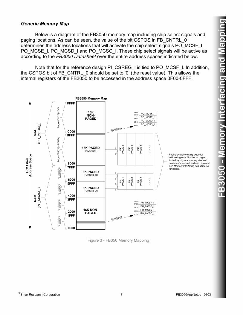
Generic Memory Map Below is a diagram of the FB3050 memory map including chip select signals and paging locations. As can be seen, the value of the bit CSPOS in FB_CNTRL_0 determines the address locations that will activate the chip select signals PO_MCSF_I, PO_MCSE_I, PO_MCSD_I and PO_MCSC_I. These chip select signals will be active as according to the FB3050 Datasheet over the entire address spaces indicated below. Note that for the reference design PI_CSREG_I is tied to PO_MCSF_I. In addition, the CSPOS bit of FB_CNTRL_0 should be set to ‘0’ (the reset value). This allows the internal registers of the FB3050 to be accessed in the address space 0F00-0FFF.
Figure 3 - FB350 Memory Mapping
FB3050 Memory Map
16K PAGED(ROMSeg)
16KNON-
PAGED
8K PAGED(RAMSeg_B)
16K NON-PAGED
0000
7FFF8000
FFFF
HC
11 6
4KA
ddre
ss S
pace
16K
PAG
E 1
16K
PAG
E 2
16K
PAG
E 3
. . .
. .
Paging available using extendedaddressing only. Number of pageslimited by physical memory size andnumber of extended address bits used.See Memory Interfacing and Mappingfor details.
RAM
(PO
_MR
AM_I
)R
OM
(PO
_MR
OM
_I)
BFFFC000
PO_MCSF_IPO_MCSE_IPO_MCSD_IPO_MCSC_I
BFFFBF00
BE00
BD00
BC00
PO_MCSF_IPO_MCSE_IPO_MCSD_IPO_MCSC_I
0FFF0F00
0E00
0D00
0C00
CSPOS=0
CSPOS=1
8K PAGED(RAMSeg_A)
8KPA
GE
1
. . .
.
8KPA
GE
2
8KPA
GE
3
5FFF6000
3FFF4000
PO_X
ADD
R[7
:0] =
0x0
0PO
_XAD
DR
[7:0
] = R
OM
Seg
1FFF2000
PO_X
ADD
R[7
:0]
= R
AMSe
g_B
PO_X
ADD
R[7
:0]
= R
AMSe
g_A
PO_X
ADD
R[7
:0]
= 0x
01PO
_XAD
DR
[7:0
]=
0x00
©Smar Research Corporation 8 FB3050AppNotes - 0303
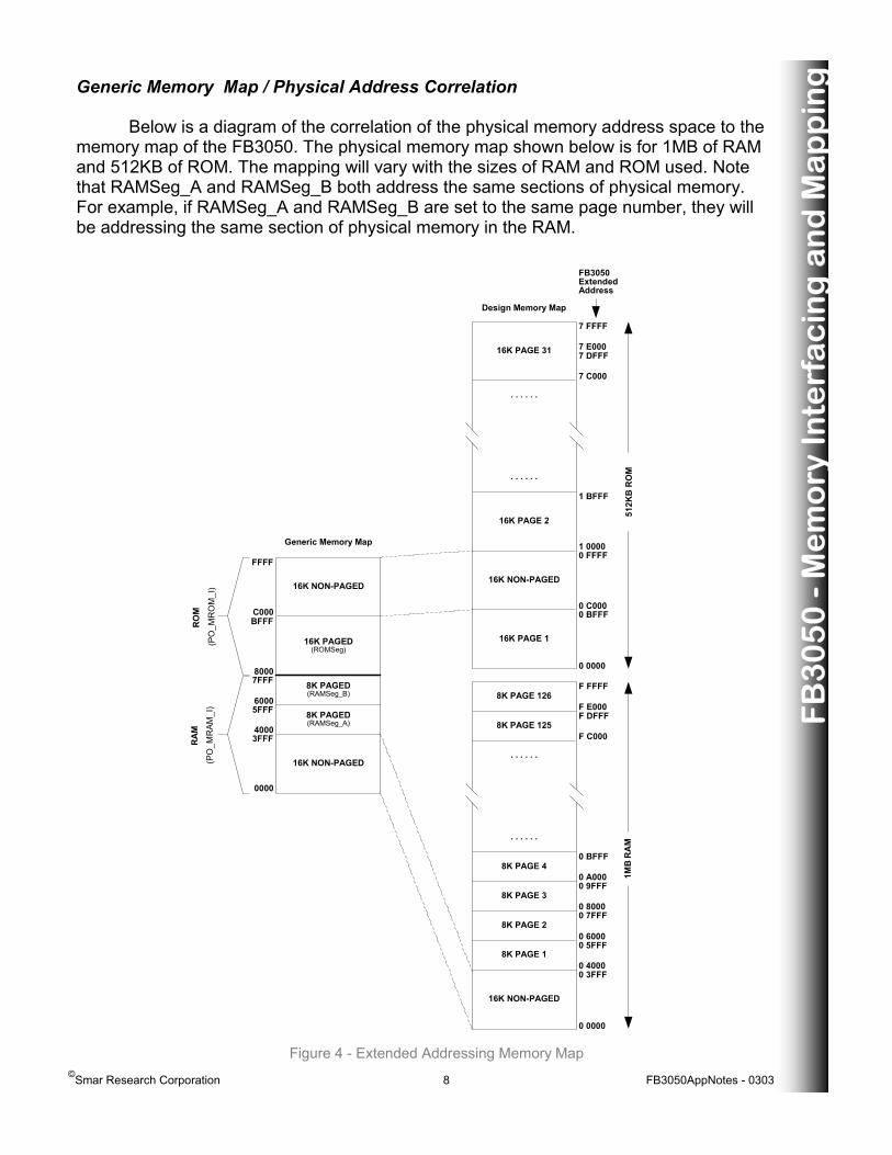
Figure 4 - Extended Addressing Memory Map
FB
30
50
- M
em
ory
Inte
rfa
cin
g a
nd
Ma
pp
ing
Generic Memory Map / Physical Address Correlation Below is a diagram of the correlation of the physical memory address space to the memory map of the FB3050. The physical memory map shown below is for 1MB of RAM and 512KB of ROM. The mapping will vary with the sizes of RAM and ROM used. Note that RAMSeg_A and RAMSeg_B both address the same sections of physical memory. For example, if RAMSeg_A and RAMSeg_B are set to the same page number, they will be addressing the same section of physical memory in the RAM.
16K PAGED(ROMSeg)
16K NON-PAGED
8K PAGED(RAMSeg_B)
16K NON-PAGED
0000
7FFF8000
FFFF
8K PAGE 1
16K NON-PAGED
16K PAGE 1
16K NON-PAGED
8K PAGE 2
8K PAGE 3
8K PAGE 125
8K PAGE 126
. . . . . .
. . . . . .
. . . . . .
. . . . . .
16K PAGE 2
16K PAGE 31
1MB
RA
M51
2KB
RO
M
0 0000
0 5FFF0 6000
0 7FFF0 8000
0 9FFF0 A000
0 BFFF
F C000
F DFFFF E000
F FFFF
FB3050ExtendedAddress
0 0000
0 FFFF1 0000
1 BFFF
7 C000
7 DFFF7 E000
7 FFFF
0 BFFF0 C000
Generic Memory Map
Design Memory Map
ROM
(PO
_MR
OM
_I)
RAM
(PO
_MR
AM_I
) 5FFF6000
BFFFC000
8K PAGED(RAMSeg_A)
3FFF4000
8K PAGE 4
0 3FFF0 4000
©Smar Research Corporation 9 FB3050AppNotes - 0303
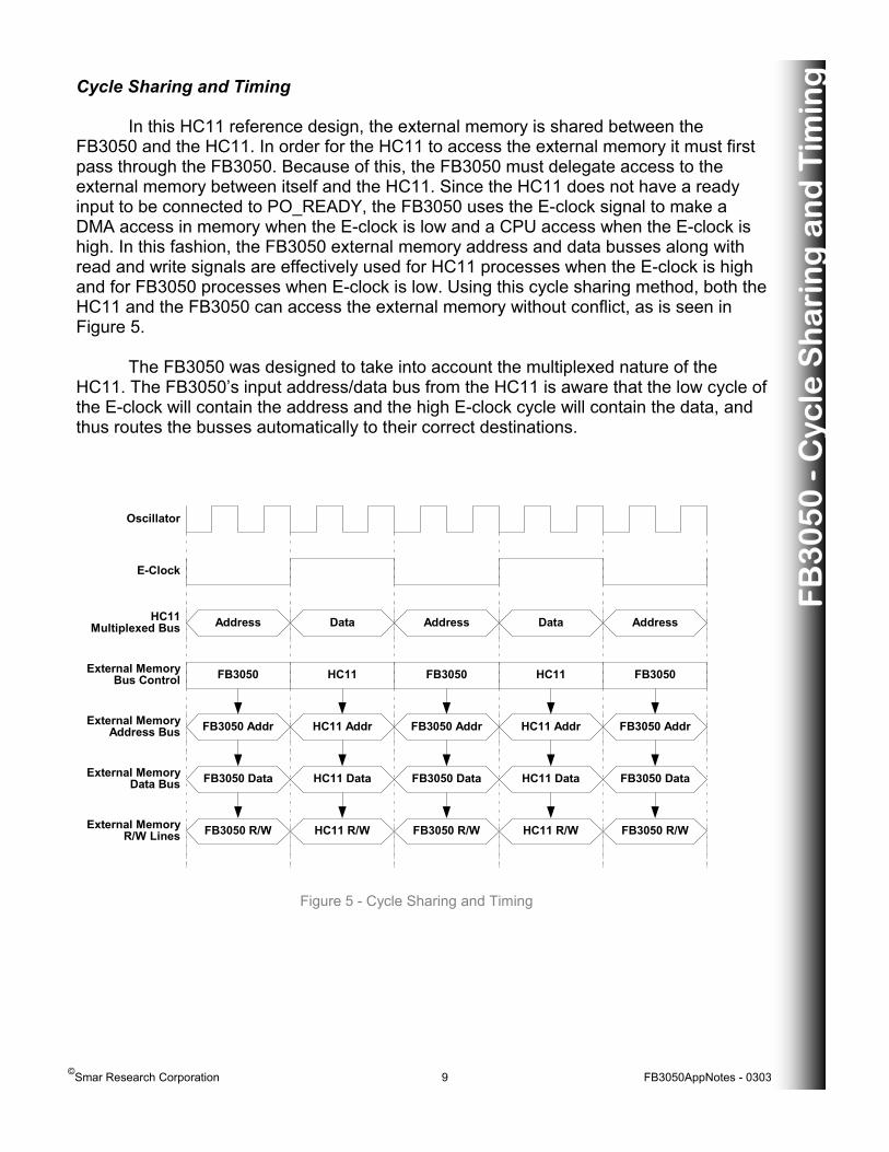
Figure 5 - Cycle Sharing and Timing
FB
30
50
- C
ycle
Sh
ari
ng
an
d T
imin
g
Cycle Sharing and Timing In this HC11 reference design, the external memory is shared between the FB3050 and the HC11. In order for the HC11 to access the external memory it must first pass through the FB3050. Because of this, the FB3050 must delegate access to the external memory between itself and the HC11. Since the HC11 does not have a ready input to be connected to PO_READY, the FB3050 uses the E-clock signal to make a DMA access in memory when the E-clock is low and a CPU access when the E-clock is high. In this fashion, the FB3050 external memory address and data busses along with read and write signals are effectively used for HC11 processes when the E-clock is high and for FB3050 processes when E-clock is low. Using this cycle sharing method, both the HC11 and the FB3050 can access the external memory without conflict, as is seen in Figure 5. The FB3050 was designed to take into account the multiplexed nature of the HC11. The FB3050’s input address/data bus from the HC11 is aware that the low cycle of the E-clock will contain the address and the high E-clock cycle will contain the data, and thus routes the busses automatically to their correct destinations.
Oscillator
E-Clock
HC11Multiplexed Bus Address Data Address Data Address
External MemoryBus Control FB3050 FB3050 FB3050HC11 HC11
FB3050 Addr HC11 Addr FB3050 Addr HC11 Addr FB3050 AddrExternal MemoryAddress Bus
FB3050 Data HC11 Data FB3050 Data HC11 Data FB3050 DataExternal MemoryData Bus
FB3050 R/W HC11 R/W FB3050 R/W HC11 R/W FB3050 R/WExternal MemoryR/W Lines
©Smar Research Corporation 10 FB3050AppNotes - 0303
FB
30
50
- M
AU
An
alo
g In
terf
ac
e
Medium Attachment Unit (MAU) Analog Interface
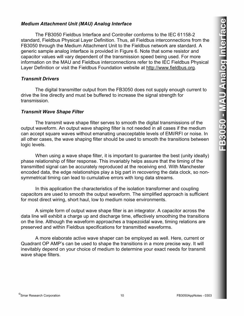
The FB3050 Fieldbus Interface and Controller conforms to the IEC 61158-2 standard, Fieldbus Physical Layer Definition. Thus, all Fieldbus interconnections from the FB3050 through the Medium Attachment Unit to the Fieldbus network are standard. A generic sample analog interface is provided in Figure 6. Note that some resistor and capacitor values will vary dependent of the transmission speed being used. For more information on the MAU and Fieldbus interconnections refer to the IEC Fieldbus Physical Layer Definition or visit the Fieldbus Foundation website at http://www.fieldbus.org.
Transmit Drivers The digital transmitter output from the FB3050 does not supply enough current to drive the line directly and must be buffered to increase the signal strength for transmission. Transmit Wave Shape Filter The transmit wave shape filter serves to smooth the digital transmissions of the output waveform. An output wave shaping filter is not needed in all cases if the medium can accept square waves without emanating unacceptable levels of EMI/RFI or noise. In all other cases, the wave shaping filter should be used to smooth the transitions between logic levels. When using a wave shape filter, it is important to guarantee the best (unity ideally) phase relationship of filter response. This invariably helps assure that the timing of the transmitted signal can be accurately reproduced at the receiving end. With Manchester encoded data, the edge relationships play a big part in recovering the data clock, so non-symmetrical timing can lead to cumulative errors with long data streams. In this application the characteristics of the isolation transformer and coupling capacitors are used to smooth the output waveform. The simplified approach is sufficient for most direct wiring, short haul, low to medium noise environments. A simple form of output wave shape filter is an integrator. A capacitor across the data line will exhibit a charge up and discharge time, effectively smoothing the transitions on the line. Although the waveform approaches a trapezoidal wave, timing relations are preserved and within Fieldbus specifications for transmitted waveforms. A more elaborate active wave shaper can be employed as well. Here, current or Quadrant OP AMP’s can be used to shape the transitions in a more precise way. It will inevitably depend on your choice of medium to determine your exact needs for transmit wave shape filters.

©Smar Research Corporation 11 FB3050AppNotes - 0303
Figure 6 - MAU Analog Interface
FB
30
50
- M
AU
An
alo
g In
terf
ac
e
Receive Band Pass Filter The receive band pass filter is important to eliminate out of band noise and interference. It also presents clean acquired signals to the FB3050 in digital form. In the example application, a single stage OP AMP bandpass filter feeds a Schmidt triggered comparator with hysteresis. The OP AMP transitional responses needed to recover the signal, span a wider band. The low frequency cutoff is dependent on line characteristics. The high frequency cutoff should be lower than any switching noise that can be induced from switching power supplies or other local oscillators. The filter has a low frequency cutoff of 250KHz (8KHz for H1) with an active signal band between 250KHz and 1.225MHz (8KHz and 40KHz for H1). This is the frequency range that we want to optimize phase delay characteristics around. The output of the filter is fed into a comparator biased as a Schmidt trigger with hysteresis. The feedback R/C values determine the hysteresis characteristics. The output is a clean square wave in digital format. The comparator functions as a zero cross detector.
TF1
1
2
35
4
FieldbusLine
+
_
6
23
6+
_23
6439
VCC
942PI_PHPDU
VCC
R4R1R3C1C2R10 300R 10R
33n 470p4.7p33p
20K 8.2K4.7K20K
100R 150R
H21M
H131.25K HC126
1 23
6 4 5
HC126
10 98
11 13 12
PO_PHPDU
PO_TACT
PO_PHPDU__________
PO_TACT
R4
C4 1uF
C5 10uF C6 10uF
R3C2
C1
R1C3
100nF
R210K
R510K
R8 1MR7 10K
C7100nF
R610K
R910K
R10

©Smar Research Corporation 12 FB3050AppNotes - 0303
FB
30
50
- S
oft
wa
re P
roc
ed
ure
s
Software Procedures The FB3050 is a powerful Fieldbus communication controller. It implements the IEC Physical Layer and some parts of the Data Link Layer Standards. Because of this, the FB3050 can be used for any Fieldbus protocol based on the IEC standards, such as the Fieldbus Foundation protocol. Also, the FB3050 can still be used for protocols that conform to the IEC Physical Layer Standard, but do not conform to the IEC Data Link Layer Standard. To do this, the specific IEC Data Link Layer features included in the chip, such as Address Recognition, can be disabled. This section contains a comprehensive look at the various software procedures of the FB3050. This includes detailed explanations as well as sample ANSI-C code for all the major functions of the FB3050. The following software procedures will be discussed: • Communication
• DMA Reception • DMA Transmission • Address Recognition
• System Timers • Timer Comparator Driven Interrupt
Each application that is explained will contain the following sub-sections: • Purpose: will explain the goal and purpose of the application • Registers Involved: contains a list of registers that will be of particular interest • Method: contains all information needed to realize the application • Code: contains sample ANSI-C code that realizes the application Header File Before we discuss the details of writing software procedures for the FB3050 it is desirable to create a header file that will contain easily readable names for the internal registers of the FB3050. This header file will map the names of the FB3050 internal registers as stated in the FB3050 Datasheet to their physical addresses as specified in the reference design. This header file will then be included in all ‘C’ programs created in this document. The reference header file can be seen on the following page. It should be noted that this header file is to be used as a reference only. Different hardware designs may have different address ranges mapped to the FB3050 internal registers. In addition, syntax may vary between different compilers and/or assemblers.

©Smar Research Corporation 13 FB3050AppNotes - 0303
FB
30
50
- S
oft
wa
re P
roc
ed
ure
s
/*----------------------------------------------------------------------------- ---------------------------------------- | | FB3050.h | | Include File for FB3050 global register definition | | | | This file contains address definitions for the FB3050 Internal registers in C format | | | -----------------------------------------------------------------------------------------------------------------------*/ #define fb_base 0x0F00 #define RCV_REG (* (unsigned char*) (fb_base+0)) #define TRM_REG (* (unsigned char*) (fb_base+0)) #define FB_CNTRL_0 (* (unsigned char*) (fb_base+1)) #define FB_CNTRL_1 (* (unsigned char*) (fb_base+2)) #define ISR_MSTR (* (unsigned char*) (fb_base+3)) #define FB_CNTRL_2 (* (unsigned char*) (fb_base+3)) #define ISR_0 (* (unsigned char*) (fb_base+4)) #define ISR_1 (* (unsigned char*) (fb_base+5)) #define ISR_2 (* (unsigned char*) (fb_base+6)) #define ISR_3 (* (unsigned char*) (fb_base+7)) #define IMS_0 (* (unsigned char*) (fb_base+8)) #define IMS_1 (* (unsigned char*) (fb_base+9)) #define IMS_2 (* (unsigned char*) (fb_base+10)) #define IMS_3 (* (unsigned char*) (fb_base+11)) #define TRM_ByteCnt (* (unsigned int*) (fb_base+12)) #define TRM_ByteCnt_Hi (* (unsigned char*) (fb_base+12)) #define TRM_ByteCnt_Lo (* (unsigned char*) (fb_base+13)) #define TRM_BufferPtr (* (unsigned int*) (fb_base+14)) #define TRM_BufferPtr_Hi (* (unsigned char*) (fb_base+14)) #define TRM_BufferPtr_Lo (* (unsigned char*) (fb_base+15)) #define TRM_BufferSeg (* (unsigned char*) (fb_base+16)) #define RAMSeg_B (* (unsigned char*) (fb_base+17)) #define RCV_BufferPtr (* (unsigned int*) (fb_base+18) #define RCV_BufferPtr_Hi (* (unsigned char*) (fb_base+18)) #define RCV_BufferPtr_Lo (* (unsigned char*) (fb_base+19)) #define RCV_BufferSeg (* (unsigned char*) (fb_base+20)) #define ROMSeg (* (unsigned char*) (fb_base+21)) #define Match_Vector_Hi (* (unsigned char*) (fb_base+22)) #define ADR_TableNS_Hi (* (unsigned char*) (fb_base+22)) #define Match_Vector_Lo (* (unsigned char*) (fb_base+23)) #define ADR_TableNS_Lo (* (unsigned char*) (fb_base+23)) #define Frame_Code (* (unsigned char*) (fb_base+24)) #define ADR_TablHLNS_Hi (* (unsigned char*) (fb_base+24)) #define Frame_Control (* (unsigned char*) (fb_base+25)) #define ADR_TablHLNS_Lo (* (unsigned char*) (fb_base+25)) #define ADR_TableSeg (* (unsigned char*) (fb_base+26)) #define NODE_ID (* (unsigned char*) (fb_base+27)) #define STATUS_0 (* (unsigned char*) (fb_base+28)) #define STATUS_1 (* (unsigned char*) (fb_base+29)) #define STATUS_2 (* (unsigned char*) (fb_base+30)) #define RAM_Seg_A (* (unsigned char*) (fb_base+31)) #define 132_COUNT_Hi (* (unsigned char*) (fb_base+32)) #define 132_COMP_Hi (* (unsigned char*) (fb_base+32)) #define 132_COUNT_Lo (* (unsigned char*) (fb_base+33)) #define 132_COMP_Lo (* (unsigned char*) (fb_base+33)) #define 1MS_COUNT_Hi (* (unsigned char*) (fb_base+34)) #define 1MS_COMP_Hi (* (unsigned char*) (fb_base+34)) #define 1MS_COUNT_Lo (* (unsigned char*) (fb_base+35)) #define 1MS_COMP_Lo (* (unsigned char*) (fb_base+35)) #define OCT_COUNT_Hi (* (unsigned char*) (fb_base+36)) #define OCT_COMP_Hi (* (unsigned char*) (fb_base+36)) #define OCT_COUNT_Lo (* (unsigned char*) (fb_base+37)) #define OCT_COMP_Lo (* (unsigned char*) (fb_base+37))
Example Code 1 - FB3050 Internal Register Header File
©Smar Research Corporation 14 FB3050AppNotes - 0303
FB
30
50
- S
oft
wa
re P
roc
ed
ure
s -
DM
A M
ess
ag
e R
ec
ep
tio
n
DMA Message Reception Purpose The FB3050 has a direct memory access scheme that greatly facilitates the reception task. With this DMA scheme, the FB3050 can save received messages directly to the memory, without needing CPU intervention. The user only needs to specify which memory area will be used for the reception buffer. The FB3050 will put the messages in the buffer sequentially, in the order they are received. The reception buffer needs a 4 KB contiguous memory space. This buffer is cyclic, so when the end of the buffer is reached, the FB3050 will return the buffer pointer to the buffer beginning and will continue writing the next received bytes there. Registers Involved RCV_BufferPtr_Hi and RCV_BufferPtr_Lo These two registers are used to specify the pointer to the reception buffer. This pointer represents a 16 bit address. When written, it specifies the start of the buffer. The start address must be within a 4 KB boundary. When read, it gives the actual position of the pointer within the buffer space, which is the position where the next received byte will be written. After a message is received, this pointer will contain the address of the byte just after the last byte of the message. RCV_BufferSeg In a paged memory system, this register will contain the value of the segment (page) where the reception buffer is located. In a non paged memory system, it will have the most significant 8 bits of a 24 bit address, specifying the reception buffer location. FB_CONTRL_0 Bit 5 (RDE-Receive Data Enable) must be set to enable message reception. FB_CNTRL_1 Bit 1 (DRE-DMA Receive Enable) must be set to enable DMA reception. ISR_0 This register contains some interrupts related to the reception. They are: RIF - bit 2: Generated when a received message finishes. REDF - bit 3: Generated when a valid End Delimiter detected. RSDF - bit 5: Generated when a valid Start Delimiter is detected. RAF - bit 6: This interrupt is generated whenever Fieldbus data is detected. It is used to indicate bus activity. IMS_0 This mask register has the same bit assignment as ISR_0. A logic 1 enables the corresponding interrupt, while a logic 0 disables the interrupt. ISR_MSTR Bit 0 of this register (CISF) enables (logic 1) or disables (logic 0) all the communication interrupts

©Smar Research Corporation 15 FB3050AppNotes - 0303
FB
30
50
- S
oft
wa
re P
roc
ed
ure
s -
DM
A M
ess
ag
e R
ec
ep
tio
n
Method This routine uses two pointers to keep track of Start and End of Message 1) Set RCV_BufferPtr = Start of Reception Buffer 2) Set MessageStartPtr = BufferPtr 3) Set MessageEndPtr = BufferPtr 4) Enable interrupt Receiver End Delimiter (REDF - bit 3 of IMS_0) 5) Enable master Communication Interrupt (CISF - bit 0 of ISR_MSTR) 6) Enable Reception DMA (DRE - bit 1 of FB_CNTRL_1) 7) Enable Receive Data (RDE - bit 5 of FB_CNTRL_0) 8) When a REDF is detected: 8.1) Clear the interrupt 8.2) Set MessageEndPtr = BufferPtr-1 8.3) Set NextMessageStartPtr = BufferPtr 8.4) Verify and Process Message Code The code below receives Fieldbus messages and keeps track of the start and end of the current message. The processing of the individual messages has been left as an exercise for the user. /*----------------------------------------------------------------------------------------------------------------------- |
| FB3050 DMA Reception | | | | This program receives data using the DMA of the FB3050. | | | -------------------------------------------------------------------------------------------------------------------------*/ #include "fb3050.h" void main(void) { unsigned int MessageStartPtr,MessageEndPtr,NextMessageStartPtr; RCV_BufferPtr_Hi = 0x20; //STEP 1: set reception buffer address RCV_BufferPtr_Lo = 0x00; MessageStartPtr = RCV_BufferPtr; //STEP 2: set initial message start pointer MessageEndPtr = RCV_BufferPtr; //STEP 3: set initial message end pointer IMS_0 = 0x08; //STEP 4: enable REDF ISR_MSTR = 0x01; //STEP 5: enable Communication interrupts FB_CNTRL_1 = 0x02; //STEP 6: enable DRE FB_CNTRL_0 = 0x20; //STEP 7: enable RDE while (1) //infinite loop { while ((ISR_0 & 0x08) != 0x08) { } //STEP 8: wait until REDF ISR_0 = 0xFF; //STEP 8.1: clear the interrupt MessageEndPtr = RCV_Buffer - 1; //STEP 8.2: set message end NextMessageStartPtr = RCV_Buffer; //STEP 8.3: set next message start /*INSERT USER DEFINED MESSAGE PROCESSING HERE*/ } //end while } //end main
Example Code 2 - DMA Reception
©Smar Research Corporation 16 FB3050AppNotes - 0303
FB
30
50
- S
oft
wa
re P
roc
ed
ure
s -
DM
A M
ess
ag
e T
ran
smis
sio
n
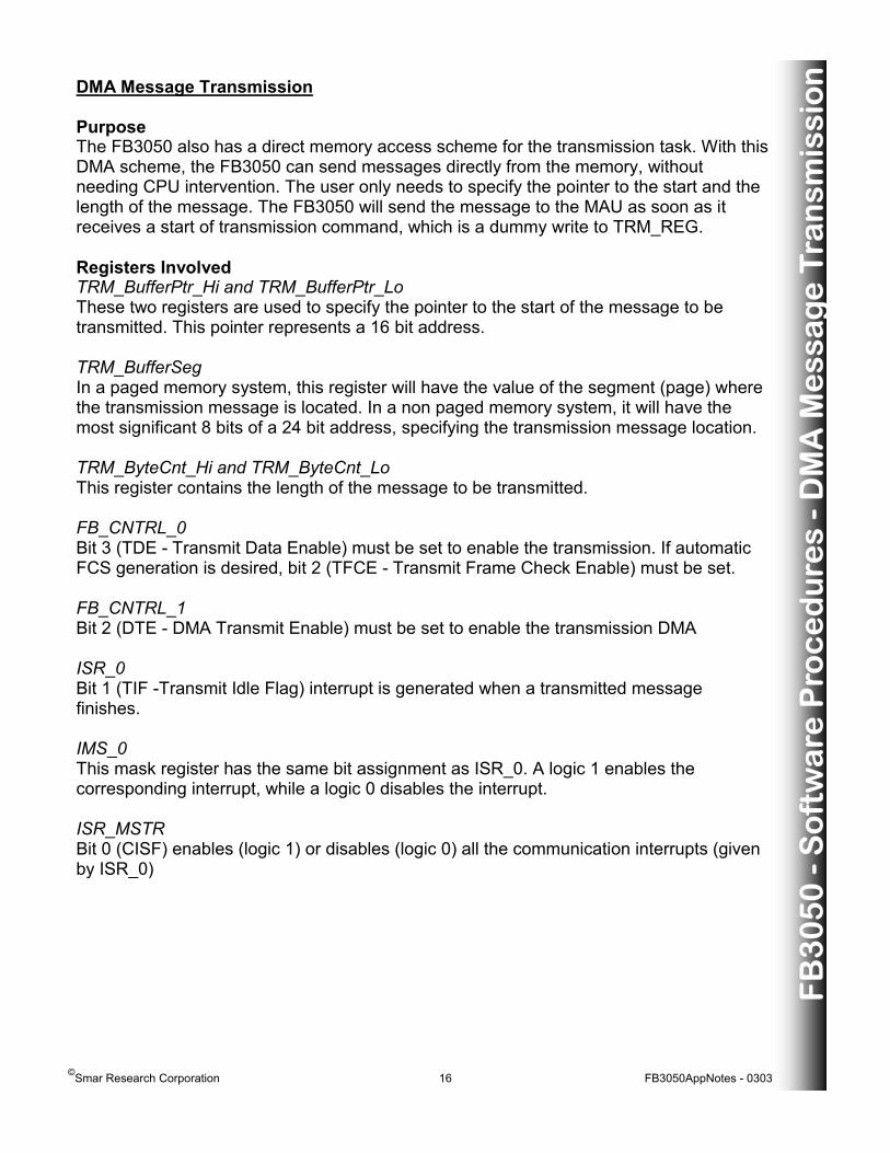
DMA Message Transmission Purpose The FB3050 also has a direct memory access scheme for the transmission task. With this DMA scheme, the FB3050 can send messages directly from the memory, without needing CPU intervention. The user only needs to specify the pointer to the start and the length of the message. The FB3050 will send the message to the MAU as soon as it receives a start of transmission command, which is a dummy write to TRM_REG. Registers Involved TRM_BufferPtr_Hi and TRM_BufferPtr_Lo These two registers are used to specify the pointer to the start of the message to be transmitted. This pointer represents a 16 bit address. TRM_BufferSeg In a paged memory system, this register will have the value of the segment (page) where the transmission message is located. In a non paged memory system, it will have the most significant 8 bits of a 24 bit address, specifying the transmission message location. TRM_ByteCnt_Hi and TRM_ByteCnt_Lo This register contains the length of the message to be transmitted. FB_CNTRL_0 Bit 3 (TDE - Transmit Data Enable) must be set to enable the transmission. If automatic FCS generation is desired, bit 2 (TFCE - Transmit Frame Check Enable) must be set. FB_CNTRL_1 Bit 2 (DTE - DMA Transmit Enable) must be set to enable the transmission DMA ISR_0 Bit 1 (TIF -Transmit Idle Flag) interrupt is generated when a transmitted message finishes. IMS_0 This mask register has the same bit assignment as ISR_0. A logic 1 enables the corresponding interrupt, while a logic 0 disables the interrupt. ISR_MSTR Bit 0 (CISF) enables (logic 1) or disables (logic 0) all the communication interrupts (given by ISR_0)
©Smar Research Corporation 17 FB3050AppNotes - 0303
FB
30
50
- S
oft
wa
re P
roc
ed
ure
s -
DM
A M
ess
ag
e T
ran
smis
sio
n
Method 1) Enable baud rate and mode (FB_CNTRL_2) 2) Load message to be sent into memory 3) Enable Transmit Idle interrupt (TIF - bit 1 of IMS_0) 4) Enable master Communication Interrupt (CISF - bit 0 of ISR_MSTR) 5) Enable Transmission DMA (DTE - bit 2 of FB_CNTRL_1) 6) Enable Transmit Data and Frame Check (TDE,TFCE bits 3and 2 of FB_CNTRL_0) 7) Transmit the message: 5.1) Set TRM_BufferPtr = Start of message to be transmitted 5.2) Set TRM_BufferSeg = Segment (page) of message to be transmitted 5.3) Set TRM_ByteCnt = Length of the message 5.4) Start message transmission (write dummy value to TRM_REG) 5.5) When TIF is detected, verify and clear the interrupt. A new message can then be transmitted. Code The code below transmits Fieldbus messages. A probe response message is sent repeatedly in an infinite loop.
/*----------------------------------------------------------------------------------------------------------------------- | | FB3050 DMA Transmission | | | | This program transmits data using the DMA of the FB3050. | | | -------------------------------------------------------------------------------------------------------------------------*/ #include "fb3050.h" #define TXBuffer (unsigned char*) (0x3000) void main(void) { unsigned int MessageStartPtr,MessageEndPtr,NextMessageStartPtr; unsigned char *Tx = TXBuffer; //used to store message to be transmitted FB_CNTRL_2 = 0x2F; //STEP 1: Set transmission frequency to 31.25K H1 *TX++ = 0x27; //STEP 2: Load frame: probe response *TX++ = 0x01; //frame control = 27h (frame code = 17h) *TX++ = 0x03; *TX++ = 0x00; *TX++ = 0x00; *TX++ = 0x00; *TX++ = 0x50; *TX++ = 0x0C; *TX++ = 0xAB; IMS_0 = 0x02; //STEP 3: Enable TIF ISR_MSTR = 0x01; //STEP 4: Enable CISF FB_CNTRL_1 = 0x04; //STEP 5: Enable DTE FB_CNTRL_0 = 0x0C; //STEP 6: Enable TDE,TFCE while(1) //STEP 7: Transmit loop { TRM_BufferPtr = 0x3000; //STEP 7.1: Set transmit buffer address TRM_BufferSeg = 0x00; //STEP 7.2: Set transmit buffer segment TRM_ByteCnt = 0x0009; //STEP 7.3: Set length of transmit message TRM_REG = 0xEE; //STEP 7.4: Dummy write to start transmission while ((ISR_0 & 0x02) != 0x02) { } //STEP 7.5: wait until TIF ISR_0 = 0xFF; //clear interrupt } //end while } //end main
Example Code 3 - DMA Transmission

©Smar Research Corporation 18 FB3050AppNotes - 0303
FB
30
50
- S
oft
wa
re P
roc
ed
ure
s -
Ad
dre
ss R
ec
og
nit
ion
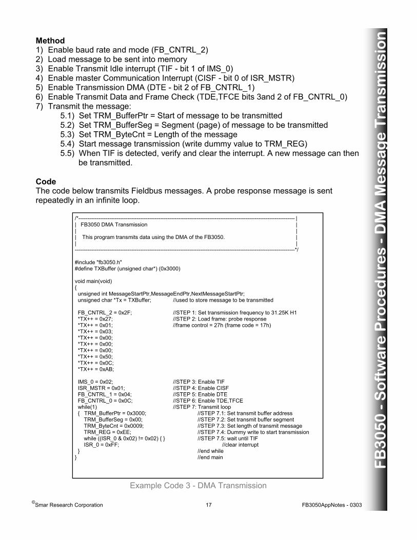
Address Recognition Purpose The FB3050 has an Address Recognition capability that allows it to detect the address on the incoming message and verify if the device needs to use that message. All these checks are done by the FB3050 without CPU intervention. The mechanism of address recognition depends on the type of the message. Messages on the IEC Data Link Layer standard cab have the following types of addressing: Messages with Node Address This is an 8-bit address. In this case the FB3050 compares the node address on the message with the value in the Node_ID register. The Node_ID register is intended to contain the Node Address of the station. An example is the Pass Token message. Node Selector (NS) Address This is a 16-bit address. In this case the FB3050 will detect the NS address on the message and compare it with the contents of a lookup table, called the NS Table. This lookup table must be filled by the user with all the NS addresses interesting to the device. Examples of these types of messages are Establish Connection and Data Transfers. Link Node Selector (HLNS) Address This is a 32-bit address. In this case the FB3050 will detect the HLNS address on the message and compare it with the contents of a lookup table, called HLNS Table. This lookup table must be filled by the user with all the HLNS addresses of interest to the device. Examples of these types of messages are the Establish Connection and Data Transfers that are being exchanged between different links. The ADR_TableNS_Hi and ADR_TableNS_Lo registers will contain the starting address of the NS table. The ADR_TableHLNS_Hi and ADR_TableHLNS_Lo registers will contain the starting address of the HLNS table. The ADR_TableSeg will contain the segment (page) where both tables are located. The mechanism for the lookup is the same for either of the two tables. The FB3050 will start the lookup in the address given by the ADR_Table registers and will continue until a match or the end of the table is found. The end of the table is defined by three consecutive zero bytes or words. The only difference between the two tables is that for the NS Table the comparison is made with 16-bit values, while for the HLNS Table the comparison is made with 32-bit values. When a match is found, the Match_Vector_Hi and Match_Vector_Lo registers will have the address of the table position that is one position higher than where the match was found. Broadcast Messages These types of messages are intended for all stations on the bus. When the FB3050 detects this type of message, it will sign it through the broadcast interrupt (BMDF - bit 1) in ISR_1. Examples of this type of message are the Token Return and Time Distribution. PSA Messages When a PSA message is received, a test is made to determine if the last transmit message originated at this device. If it did, an address match will occur. However, the match vector is not valid and should be disregarded. If the last transmit message originated at another device, no address match will occur.

©Smar Research Corporation 19 FB3050AppNotes - 0303
FB
30
50
- S
oft
wa
re P
roc
ed
ure
s -
Ad
dre
ss R
ec
og
nit
ion
Registers Involved FB_CNTRL_1 Bit 0 (ARME - Address Recognition Mode) must be set to enable address recognition. ISR_1 This register contains the following interrupts related to address recognition. They are: BMDF - bit 0: Generated when a broadcast message is detected. AMDF - bit 1: Generated when a match in the table is found. EOTF - bit 2: Generated when a lookup was conducted and no match as found. FCF - bit 3: Generated when the Frame Control byte on the incoming message detected. IMS_1 This mask register has the same bit assignment as ISR_1. A logic 1 enables the corresponding interrupt, while a logic 0 disables the interrupt. ISR_MSTR Bit 1 (AISF) enables (logic 1) or disables (logic 0) all the address recognition interrupts. Method 1) Set Node_ID register = Pre-selected Device Node ID 2) Fill NS and HLNS Tables 3) Set ADR_TableNS = Start of NS Table 4) Set ADR_TableHLNS = Start of HLNS Table 5) Set ADR_TableSeg = Segment (page) of NS and HLNS Tables 6) Enable interrupts Address Match and Broadcast (bits 1 and 0 of IMS_1) 7) Enable Address Unit interrupt (bit 1 of ISR_MSTR) 8) Enable DRE and Table DMA (bit 1 and 0 of FB_CNTRL_1) 9) Enable RDE (bit 5 of FB_CNTRL_0) 10) When an Address Match or Broadcast interrupt is detected, process the message Code The following code receives Fieldbus messages and checks the incoming message destination address versus address tables for a match. An address match will set an interrupt flag in the FB3050. Upon an address match, the incoming message can be appropriately processed. The processing of messages is left as an exercise for the user. It should be noted that while this example code polls the interrupt register, an interrupt service routine can also be setup using the FB3050 and the microcontroller. In this manner the code will be interrupted automatically when the address recognition interrupt is set.
©Smar Research Corporation 20 FB3050AppNotes - 0303
FB
30
50
- S
oft
wa
re P
roc
ed
ure
s -
Ad
dre
ss R
ec
og
nit
ion
/*----------------------------------------------------------------------------------------------------------------------- | | FB3050 Address Recognition | | | | This program receives Fieldbus messages and checks for an address match. | | | -------------------------------------------------------------------------------------------------------------------------*/ #include "fb3050.h" #define TXBuffer (unsigned char*) (0x3000) #define RXBuffer (unsigned char*) (0x2000) #define TableNS (unsigned char*) (0x4000) #define TableHL (unsigned char*) (0x5000) void main(void) { unsigned char *Rx = RXBuffer; //used to store message to be transmitted unsigned char *NS = TableNS; //used to store NS lookup table unsigned char *HL = TableHL; //used to store HL lookup table NODE_ID = 0xF7; //STEP 1: Set device Node ID //STEP 2: Create NS and HL tables //create NS address lookup table starting at 4000h *NS++ = 0x19; //1900h *NS++ = 0x00; *NS++ = 0x19; //19F7h *NS++ = 0xF7; *NS++ = 0x22; //2221h *NS++ = 0x21; *NS++ = 0x00; //three bytes of 00 ends the table *NS++ = 0x00; *NS++ = 0x00; //create HLNS address lookup table starting at 5000h *HL++ = 0x11; //11112222h *HL++ = 0x11; *HL++ = 0x22; *HL++ = 0x22; *HL++ = 0x11; //11113333h *HL++ = 0x11; *HL++ = 0x33; *HL++ = 0x33; *HL++ = 0x00; //three words of 00 ends table *HL++ = 0x00; *HL++ = 0x00; *HL++ = 0x00; *HL++ = 0x00; *HL++ = 0x00; ADR_TableNS_Hi = 0x40; //STEP 3: Set start of NS Table ADR_TableNS_Lo = 0x00; ADR_TableHL_Hi = 0x50; //STEP 4: Set start of HLNS Table ADR_TableHL_Lo = 0x00; ADR_TableSeg = 0x00; //STEP 5: Set segment of tables IMS_1 = 0x03; //STEP 6: Enable AMDF and BMDF ISR_MSTR = 0x02; //STEP 7: Enable AISF FB_CNTRL_1 = 0x03; //STEP 8: Enable DRE and ARME FB_CNTRL_0 = 0x20; //STEP 9: Enable RDE while ((ISR_MSTR & 0x02) != 0x02) { } //STEP 10: wait for address match interrupt /* INSERT USER DEFINED MESSAGE PROCESSING HERE */ ISR_1 = 0xFF; //clear interrupts } //end main
Example Code 4 - Address Recognition
©Smar Research Corporation 21 FB3050AppNotes - 0303
FB
30
50
- S
oft
wa
re P
roc
ed
ure
s -
Tim
er
Co
mp
ara
tor
Timers Purpose The FB3050 has a set of timers intended to facilitate the implementation of the protocol. Three timers are available: • 1/32 ms base timing • 1ms base timing • Octet base timing All three timers can be used as free running or time-out, with corresponding interrupts. When a timer is used as free running, an interrupt is generated on overflow. When it is used as a time-out, values must be written in the compare registers. The timer action is to increment the counter value continuously. When the counter value reaches the value on the compare register, an interrupt is generated. Note: When reading a timer, it is necessary to first read the high byte followed by the low byte of the timer. This is an inherent feature of the FB3050. When the high byte of a timer is read, the timer subsystem will stop counting and will resume after the high byte is read. In this manner a timer value will not have to be read “on the fly”. Registers Involved ISR_2 This register contains the following interrupts related to the timers: 1/32OF - bit 0: Generated when an 1/32 ms overflow is detected. 1/32CF - bit 1: Generated when an 1/32 ms count comparison is detected. 1OF - bit 2: Generated when an 1 ms overflow is detected. 1CF - bit 3: Generated when an 1 ms count comparison is detected. OOF - bit 4: Generated when an octet overflow is detected. OCF - bit 5: Generated when an octet count comparison is detected. IMS_2 This mask register has the same bit assignment as ISR_2. A logic 1 enables the corresponding interrupt, while a logic 0 disables the interrupt. ISR_MSTR Bit 2 (TISF) enables (logic 1) or disables (logic 0) all the timer interrupts (given by ISR_2). Method 1) Clear any interrupts in ISR_2 2) Enable baud rate and mode (FB_CNTRL_2) 3) Unmask counter to be used (IMS_2) 4) Enable Timer interrupts (bit 2 of IS_MSTR) 5) Write corresponding timer comparator registers with time to interrupt at 6) Enable interrupts Address Match and Broadcast (bits 1 and 0 of IMS_1) 7) When a Timer Interrupt is detected, run user defined process.
©Smar Research Corporation 22 FB3050AppNotes - 0303
FB
30
50
- S
oft
wa
re P
roc
ed
ure
s -
Tim
er
Co
mp
ara
tor
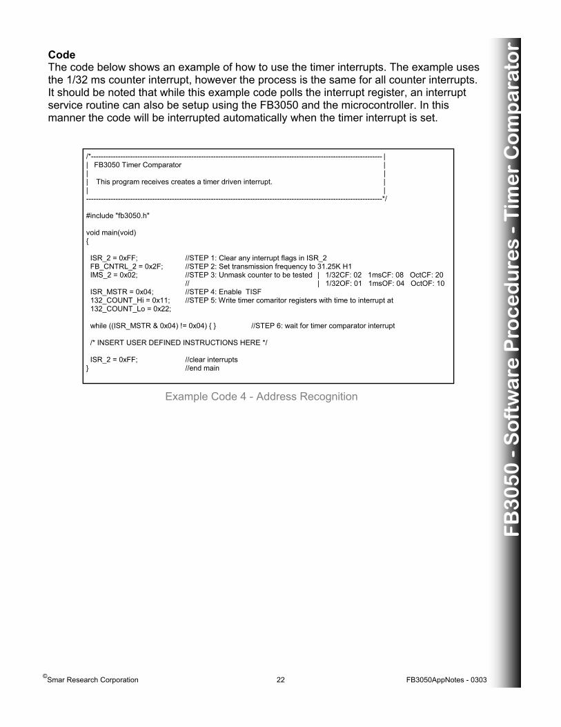
Code The code below shows an example of how to use the timer interrupts. The example uses the 1/32 ms counter interrupt, however the process is the same for all counter interrupts. It should be noted that while this example code polls the interrupt register, an interrupt service routine can also be setup using the FB3050 and the microcontroller. In this manner the code will be interrupted automatically when the timer interrupt is set.
/*----------------------------------------------------------------------------------------------------------------------- | | FB3050 Timer Comparator | | | | This program receives creates a timer driven interrupt. | | | -------------------------------------------------------------------------------------------------------------------------*/ #include "fb3050.h" void main(void) { ISR_2 = 0xFF; //STEP 1: Clear any interrupt flags in ISR_2 FB_CNTRL_2 = 0x2F; //STEP 2: Set transmission frequency to 31.25K H1 IMS_2 = 0x02; //STEP 3: Unmask counter to be tested | 1/32CF: 02 1msCF: 08 OctCF: 20 // | 1/32OF: 01 1msOF: 04 OctOF: 10 ISR_MSTR = 0x04; //STEP 4: Enable TISF 132_COUNT_Hi = 0x11; //STEP 5: Write timer comaritor registers with time to interrupt at 132_COUNT_Lo = 0x22; while ((ISR_MSTR & 0x04) != 0x04) { } //STEP 6: wait for timer comparator interrupt /* INSERT USER DEFINED INSTRUCTIONS HERE */ ISR_2 = 0xFF; //clear interrupts } //end main
Example Code 4 - Address Recognition

©Smar Research Corporation 23 FB3050AppNotes - 0303
Smar Research Corporation 4250 Veterans Memorial Highway
Holbrook, NY USA 11741 Tel: 631.737.3111 Fax: 631.737.3892
[email protected] www.SmarResearch.com
Smar Research reserves the right to make changes to design and functionality of any product without notice. Smar Research does not assume any liability arising out of the application or use of any product. Smar Research , Technology Source, and the SRC logo are registered trademarks of Smar Research Corporation. The HART, Fieldbus, and Profibus Foundation logos are
trademarks of their respective owners.