smartfusion2 soc fpga fabric architecture user’s …new.zlgmcu.com/uploadfiles/microsemi/users...
TRANSCRIPT

SmartFusion2 SoC FPGA FabricArchitecture User’s Guide

SmartFusion2 SoC FPGA Fabric Architecture User’s Guide
Revision 1 2
Table of Contents
1 Fabric Architecture . . . . . . . . . . . . . . . . . . . . . . . . . . . . . . . . . . . . . . . . . . . . . . . . . . . . . . . . . . . . . . . . .-5Introduction . . . . . . . . . . . . . . . . . . . . . . . . . . . . . . . . . . . . . . . . . . . . . . . . . . . . . . . . . . . . . . . . . . . . . . . . . . . . . . . 5
Logic Module . . . . . . . . . . . . . . . . . . . . . . . . . . . . . . . . . . . . . . . . . . . . . . . . . . . . . . . . . . . . . . . . . . . . . . . . . . . . . . 6
Interface Logic . . . . . . . . . . . . . . . . . . . . . . . . . . . . . . . . . . . . . . . . . . . . . . . . . . . . . . . . . . . . . . . . . . . . . . . . . . . . . 7
I/O Modules . . . . . . . . . . . . . . . . . . . . . . . . . . . . . . . . . . . . . . . . . . . . . . . . . . . . . . . . . . . . . . . . . . . . . . . . . . . . . . . 7
FPGA Routing Architecture . . . . . . . . . . . . . . . . . . . . . . . . . . . . . . . . . . . . . . . . . . . . . . . . . . . . . . . . . . . . . . . . . . . 9
Fabric Array Coordinate System . . . . . . . . . . . . . . . . . . . . . . . . . . . . . . . . . . . . . . . . . . . . . . . . . . . . . . . . . . . . . . 12
Glossary . . . . . . . . . . . . . . . . . . . . . . . . . . . . . . . . . . . . . . . . . . . . . . . . . . . . . . . . . . . . . . . . . . . . . . . . . . . . . . . . . 13
2 LSRAM . . . . . . . . . . . . . . . . . . . . . . . . . . . . . . . . . . . . . . . . . . . . . . . . . . . . . . . . . . . . . . . . . . . . . . . . .-15Introduction . . . . . . . . . . . . . . . . . . . . . . . . . . . . . . . . . . . . . . . . . . . . . . . . . . . . . . . . . . . . . . . . . . . . . . . . . . . . . . 15
Port List . . . . . . . . . . . . . . . . . . . . . . . . . . . . . . . . . . . . . . . . . . . . . . . . . . . . . . . . . . . . . . . . . . . . . . . . . . . . . . . . . 17
Port Descriptions . . . . . . . . . . . . . . . . . . . . . . . . . . . . . . . . . . . . . . . . . . . . . . . . . . . . . . . . . . . . . . . . . . . . . . . . . . 19
Operating Modes . . . . . . . . . . . . . . . . . . . . . . . . . . . . . . . . . . . . . . . . . . . . . . . . . . . . . . . . . . . . . . . . . . . . . . . . . . 23
Timing Diagrams . . . . . . . . . . . . . . . . . . . . . . . . . . . . . . . . . . . . . . . . . . . . . . . . . . . . . . . . . . . . . . . . . . . . . . . . . . 28
Reset Operation . . . . . . . . . . . . . . . . . . . . . . . . . . . . . . . . . . . . . . . . . . . . . . . . . . . . . . . . . . . . . . . . . . . . . . . . . . . 32
Collision . . . . . . . . . . . . . . . . . . . . . . . . . . . . . . . . . . . . . . . . . . . . . . . . . . . . . . . . . . . . . . . . . . . . . . . . . . . . . . . . . 32
Glossary . . . . . . . . . . . . . . . . . . . . . . . . . . . . . . . . . . . . . . . . . . . . . . . . . . . . . . . . . . . . . . . . . . . . . . . . . . . . . . . . . 33
List of Changes . . . . . . . . . . . . . . . . . . . . . . . . . . . . . . . . . . . . . . . . . . . . . . . . . . . . . . . . . . . . . . . . . . . . . . . . . . . 33
3 Micro SRAM (uSRAM) . . . . . . . . . . . . . . . . . . . . . . . . . . . . . . . . . . . . . . . . . . . . . . . . . . . . . . . . . . . . .-35Introduction . . . . . . . . . . . . . . . . . . . . . . . . . . . . . . . . . . . . . . . . . . . . . . . . . . . . . . . . . . . . . . . . . . . . . . . . . . . . . . 35
Port List . . . . . . . . . . . . . . . . . . . . . . . . . . . . . . . . . . . . . . . . . . . . . . . . . . . . . . . . . . . . . . . . . . . . . . . . . . . . . . . . . 38
Port Description . . . . . . . . . . . . . . . . . . . . . . . . . . . . . . . . . . . . . . . . . . . . . . . . . . . . . . . . . . . . . . . . . . . . . . . . . . . 39
Read Operation . . . . . . . . . . . . . . . . . . . . . . . . . . . . . . . . . . . . . . . . . . . . . . . . . . . . . . . . . . . . . . . . . . . . . . . . . . . 43
Write Operation . . . . . . . . . . . . . . . . . . . . . . . . . . . . . . . . . . . . . . . . . . . . . . . . . . . . . . . . . . . . . . . . . . . . . . . . . . . 49
Collision . . . . . . . . . . . . . . . . . . . . . . . . . . . . . . . . . . . . . . . . . . . . . . . . . . . . . . . . . . . . . . . . . . . . . . . . . . . . . . . . . 52
Glossary . . . . . . . . . . . . . . . . . . . . . . . . . . . . . . . . . . . . . . . . . . . . . . . . . . . . . . . . . . . . . . . . . . . . . . . . . . . . . . . . . 52
List of Changes . . . . . . . . . . . . . . . . . . . . . . . . . . . . . . . . . . . . . . . . . . . . . . . . . . . . . . . . . . . . . . . . . . . . . . . . . . . 52
4 Mathblocks . . . . . . . . . . . . . . . . . . . . . . . . . . . . . . . . . . . . . . . . . . . . . . . . . . . . . . . . . . . . . . . . . . . . . .-53Introduction . . . . . . . . . . . . . . . . . . . . . . . . . . . . . . . . . . . . . . . . . . . . . . . . . . . . . . . . . . . . . . . . . . . . . . . . . . . . . . 53
Mathblock Architectural Overview . . . . . . . . . . . . . . . . . . . . . . . . . . . . . . . . . . . . . . . . . . . . . . . . . . . . . . . . . . . . . 53
Using Mathblock . . . . . . . . . . . . . . . . . . . . . . . . . . . . . . . . . . . . . . . . . . . . . . . . . . . . . . . . . . . . . . . . . . . . . . . . . . 57
Mathblock Applications . . . . . . . . . . . . . . . . . . . . . . . . . . . . . . . . . . . . . . . . . . . . . . . . . . . . . . . . . . . . . . . . . . . . . 65
Coding Style Examples . . . . . . . . . . . . . . . . . . . . . . . . . . . . . . . . . . . . . . . . . . . . . . . . . . . . . . . . . . . . . . . . . . . . . 68
Glossary . . . . . . . . . . . . . . . . . . . . . . . . . . . . . . . . . . . . . . . . . . . . . . . . . . . . . . . . . . . . . . . . . . . . . . . . . . . . . . . . . 72
List of Changes . . . . . . . . . . . . . . . . . . . . . . . . . . . . . . . . . . . . . . . . . . . . . . . . . . . . . . . . . . . . . . . . . . . . . . . . . . . 72
5 Fabric Global Routing Resources . . . . . . . . . . . . . . . . . . . . . . . . . . . . . . . . . . . . . . . . . . . . . . . . . . . .-73Global Routing Network . . . . . . . . . . . . . . . . . . . . . . . . . . . . . . . . . . . . . . . . . . . . . . . . . . . . . . . . . . . . . . . . . . . . . 73
Clocking Resources . . . . . . . . . . . . . . . . . . . . . . . . . . . . . . . . . . . . . . . . . . . . . . . . . . . . . . . . . . . . . . . . . . . . . . . . 78
Connection of Dedicated Global I/Os to GBs . . . . . . . . . . . . . . . . . . . . . . . . . . . . . . . . . . . . . . . . . . . . . . . . . . . . . 80
Glossary . . . . . . . . . . . . . . . . . . . . . . . . . . . . . . . . . . . . . . . . . . . . . . . . . . . . . . . . . . . . . . . . . . . . . . . . . . . . . . . . . 83
List of Changes . . . . . . . . . . . . . . . . . . . . . . . . . . . . . . . . . . . . . . . . . . . . . . . . . . . . . . . . . . . . . . . . . . . . . . . . . . . 84

SmartFusion2 SoC FPGA Fabric Architecture User’s Guide
Revision 1 3
6 I/Os. . . . . . . . . . . . . . . . . . . . . . . . . . . . . . . . . . . . . . . . . . . . . . . . . . . . . . . . . . . . . . . . . . . . . . . . . . . .-85Overview . . . . . . . . . . . . . . . . . . . . . . . . . . . . . . . . . . . . . . . . . . . . . . . . . . . . . . . . . . . . . . . . . . . . . . . . . . . . . . . . 85
I/O Functional Description . . . . . . . . . . . . . . . . . . . . . . . . . . . . . . . . . . . . . . . . . . . . . . . . . . . . . . . . . . . . . . . . . . . 85
I/O Banks . . . . . . . . . . . . . . . . . . . . . . . . . . . . . . . . . . . . . . . . . . . . . . . . . . . . . . . . . . . . . . . . . . . . . . . . . . . . . . . . 89
Supported I/O Standards . . . . . . . . . . . . . . . . . . . . . . . . . . . . . . . . . . . . . . . . . . . . . . . . . . . . . . . . . . . . . . . . . . . . 90
I/O Programmable Features . . . . . . . . . . . . . . . . . . . . . . . . . . . . . . . . . . . . . . . . . . . . . . . . . . . . . . . . . . . . . . . . . 93
I/Os in Conjunction with Fabric, MDDR/FDDR, and MSS Peripherals . . . . . . . . . . . . . . . . . . . . . . . . . . . . . . . . 103
JTAG I/O . . . . . . . . . . . . . . . . . . . . . . . . . . . . . . . . . . . . . . . . . . . . . . . . . . . . . . . . . . . . . . . . . . . . . . . . . . . . . . . 104
Dedicated I/O . . . . . . . . . . . . . . . . . . . . . . . . . . . . . . . . . . . . . . . . . . . . . . . . . . . . . . . . . . . . . . . . . . . . . . . . . . . . 106
Glossary . . . . . . . . . . . . . . . . . . . . . . . . . . . . . . . . . . . . . . . . . . . . . . . . . . . . . . . . . . . . . . . . . . . . . . . . . . . . . . . . 114
7 List of Changes . . . . . . . . . . . . . . . . . . . . . . . . . . . . . . . . . . . . . . . . . . . . . . . . . . . . . . . . . . . . . . . . .-117List of Changes . . . . . . . . . . . . . . . . . . . . . . . . . . . . . . . . . . . . . . . . . . . . . . . . . . . . . . . . . . . . . . . . . . . . . . . . . . 117
A Product Support . . . . . . . . . . . . . . . . . . . . . . . . . . . . . . . . . . . . . . . . . . . . . . . . . . . . . . . . . . . . . . . . .-119Customer Service . . . . . . . . . . . . . . . . . . . . . . . . . . . . . . . . . . . . . . . . . . . . . . . . . . . . . . . . . . . . . . . . . . . . . . . . 119
Customer Technical Support Center . . . . . . . . . . . . . . . . . . . . . . . . . . . . . . . . . . . . . . . . . . . . . . . . . . . . . . . . . . 119
Technical Support . . . . . . . . . . . . . . . . . . . . . . . . . . . . . . . . . . . . . . . . . . . . . . . . . . . . . . . . . . . . . . . . . . . . . . . . 119
Website . . . . . . . . . . . . . . . . . . . . . . . . . . . . . . . . . . . . . . . . . . . . . . . . . . . . . . . . . . . . . . . . . . . . . . . . . . . . . . . . 119
Contacting the Customer Technical Support Center . . . . . . . . . . . . . . . . . . . . . . . . . . . . . . . . . . . . . . . . . . . . . . 119
ITAR Technical Support . . . . . . . . . . . . . . . . . . . . . . . . . . . . . . . . . . . . . . . . . . . . . . . . . . . . . . . . . . . . . . . . . . . . 120


Revision 1 5
1 – Fabric Architecture
This section of the user's guide serves as a technical resource to describe the field programmable gatearray (FPGA) fabric architecture in SmartFusion®2 system-on-chip (SoC) FPGA devices.
IntroductionThe SmartFusion2 SoC FPGA fabric comprises an array of various logic modules and embedded hardblocks such as Large Static Random Access Memory (LSRAMs), Micro SRAMs (uSRAMs), mathblocks,and clock-conditioning circuits (CCCs). These elements are arranged as several rows inside the fabric,interconnected by the clustered routing architecture of SmartFusion2 SoC FPGA device. Each elementin the fabric has a distinct logical co-ordinate value assigned to it.
The types of logic elements that constitute the major part of the fabric are:
• Logic Modules
• Interface Modules
• I/O Modules
The logic module is the main logic element used for implementing combinatorial circuits, arithmeticfunctions, and sequential circuits inside the fabric. Each logic module consists of a 4-input lookup table(LUT), a D flip-flop, and a dedicated carry chain.
The interface logic is the logic module that interfaces the embedded hard blocks to the fabric routing.Interface logic enables the accessibility of the embedded hard block via the fabric routing. The interfacelogic is structurally similar to the logic module except that it does not contain the dedicated carry chain.The interface logic can also be used to implement the combinatorial and sequential circuits if theassociated embedded hard block is not being used by the design.
The I/O module forms the digital part of the fabric user I/Os: multi-standard inputs/outputs (MSIOs). TheI/O module enables the user I/Os to be connected to the fabric routing, thus enabling the routing of theexternal world signals to and from the logic elements inside the fabric.
The SmartFusion2 SoC FPGA fabric uses a clustered routing architecture to interconnect the variouselements inside the fabric. In this architecture, various logic elements are grouped together to form theclusters. Inside such clusters, the routing is denser and faster compared to routing outside the cluster,thus segmenting the routing architecture. The clustering of the routing architecture allows a more areaefficient implementation of the designs in the SmartFusion2 SoC FPGA fabric, at the same timemaintaining an optimal performance.
There are three types of clusters in the SmartFusion2 SoC FPGA fabric:
• Logic clusters
• Interface cluster
• I/O clusters
The logic cluster is composed of 12 logic modules, the interface cluster is composed of 12 interface logicelements, and I/O clusters are composed of 3 to 4 I/O modules.
However, most of the routing details are transparent to the user and the placement and routing softwaretakes care of the optimal routing implementation, depending upon the design requirements, deliveringoptimal design performance and faster compile time. The knowledge of routing architecture can be usedto guide design techniques for an efficient design implementation on the SmartFusion2 SoC FPGAfabric.
Fabric Architecture
6 Revision 1
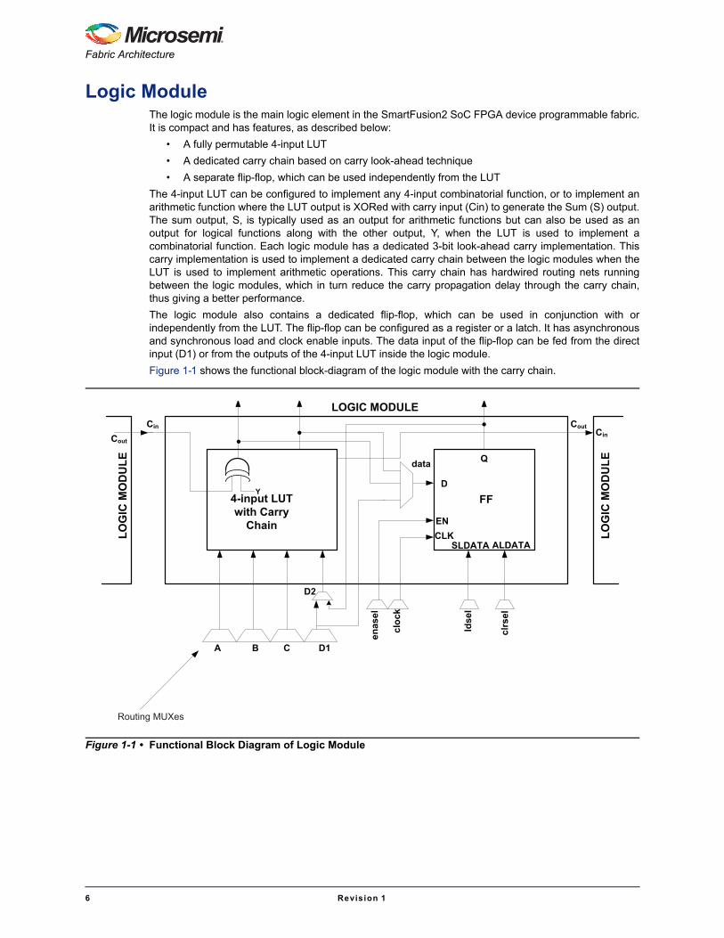
Logic ModuleThe logic module is the main logic element in the SmartFusion2 SoC FPGA device programmable fabric.It is compact and has features, as described below:
• A fully permutable 4-input LUT
• A dedicated carry chain based on carry look-ahead technique
• A separate flip-flop, which can be used independently from the LUT
The 4-input LUT can be configured to implement any 4-input combinatorial function, or to implement anarithmetic function where the LUT output is XORed with carry input (Cin) to generate the Sum (S) output.The sum output, S, is typically used as an output for arithmetic functions but can also be used as anoutput for logical functions along with the other output, Y, when the LUT is used to implement acombinatorial function. Each logic module has a dedicated 3-bit look-ahead carry implementation. Thiscarry implementation is used to implement a dedicated carry chain between the logic modules when theLUT is used to implement arithmetic operations. This carry chain has hardwired routing nets runningbetween the logic modules, which in turn reduce the carry propagation delay through the carry chain,thus giving a better performance.
The logic module also contains a dedicated flip-flop, which can be used in conjunction with orindependently from the LUT. The flip-flop can be configured as a register or a latch. It has asynchronousand synchronous load and clock enable inputs. The data input of the flip-flop can be fed from the directinput (D1) or from the outputs of the 4-input LUT inside the logic module.
Figure 1-1 shows the functional block-diagram of the logic module with the carry chain.
Figure 1-1 • Functional Block Diagram of Logic Module
Cin
Cout
A B C D1
D2
enas
el
cloc
k
clrs
el
data
CoutCin
4-input LUT with Carry
Chain
FFD
ENCLK
SLDATA ALDATA
ldse
lQ
LOGIC MODULE
LOG
IC M
OD
ULE
LOG
IC M
OD
ULE
Y
Routing MUXes
SmartFusion2 SoC FPGA Fabric Architecture User’s Guide
Revision 1 7
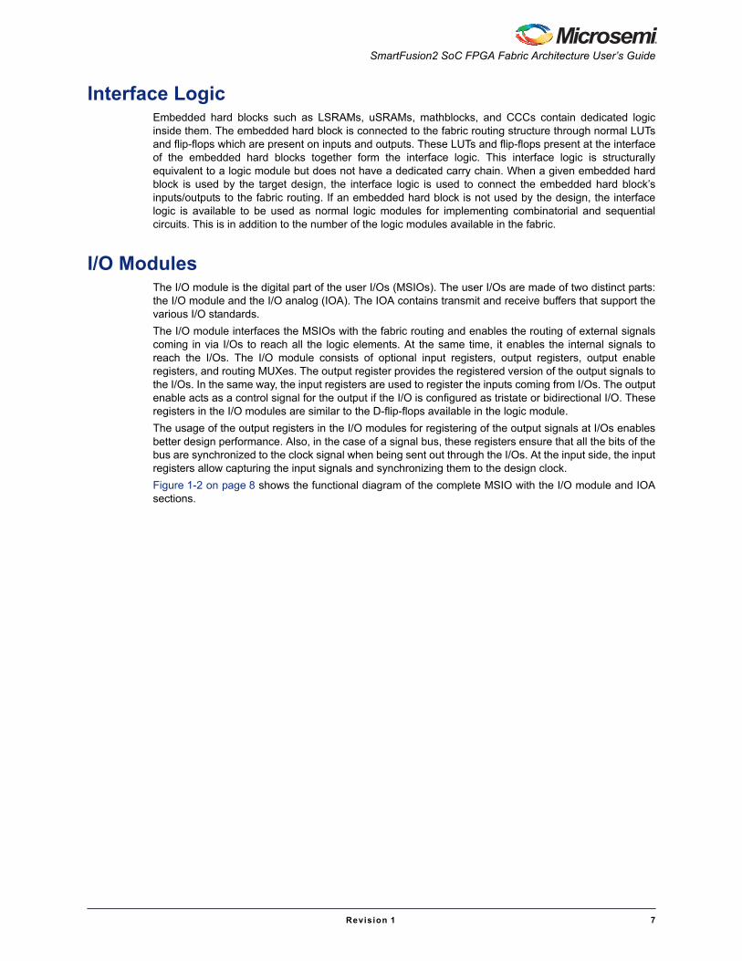
Interface LogicEmbedded hard blocks such as LSRAMs, uSRAMs, mathblocks, and CCCs contain dedicated logicinside them. The embedded hard block is connected to the fabric routing structure through normal LUTsand flip-flops which are present on inputs and outputs. These LUTs and flip-flops present at the interfaceof the embedded hard blocks together form the interface logic. This interface logic is structurallyequivalent to a logic module but does not have a dedicated carry chain. When a given embedded hardblock is used by the target design, the interface logic is used to connect the embedded hard block’sinputs/outputs to the fabric routing. If an embedded hard block is not used by the design, the interfacelogic is available to be used as normal logic modules for implementing combinatorial and sequentialcircuits. This is in addition to the number of the logic modules available in the fabric.
I/O ModulesThe I/O module is the digital part of the user I/Os (MSIOs). The user I/Os are made of two distinct parts:the I/O module and the I/O analog (IOA). The IOA contains transmit and receive buffers that support thevarious I/O standards.
The I/O module interfaces the MSIOs with the fabric routing and enables the routing of external signalscoming in via I/Os to reach all the logic elements. At the same time, it enables the internal signals toreach the I/Os. The I/O module consists of optional input registers, output registers, output enableregisters, and routing MUXes. The output register provides the registered version of the output signals tothe I/Os. In the same way, the input registers are used to register the inputs coming from I/Os. The outputenable acts as a control signal for the output if the I/O is configured as tristate or bidirectional I/O. Theseregisters in the I/O modules are similar to the D-flip-flops available in the logic module.
The usage of the output registers in the I/O modules for registering of the output signals at I/Os enablesbetter design performance. Also, in the case of a signal bus, these registers ensure that all the bits of thebus are synchronized to the clock signal when being sent out through the I/Os. At the input side, the inputregisters allow capturing the input signals and synchronizing them to the design clock.
Figure 1-2 on page 8 shows the functional diagram of the complete MSIO with the I/O module and IOAsections.

Fabric Architecture
8 Revision 1
Figure 1-2 • Functional Block Diagram of MSIO
+-
+-
Single-Ended
Pseudo-Differential
True-Differential
+-
Single-Ended
Pseudo-Differential
0
0
1
1
Tx_P
Tx_N
Rx_P
Rx_N
PAD_P
PAD_N
VREF
VREF
Differential ODT
LPE
LPE
ODT
ODT
Voltage Standard Selected
Differential/Single-ended
outreg
outreg
outreg
outreg
inreg
inreg
Output Enable
Output data
Registered Input data
Non-registered Input data
Output Enable
Output data
Non-registered Input data
Registered Input data
I/O Module IOA
Weak pull-up/pull-down resistor
control
OE_P
DO_P
DI_P
OE_N
DI_N
DO_N
Weak pull-up/pull-down resistor
control

SmartFusion2 SoC FPGA Fabric Architecture User’s Guide
Revision 1 9
FPGA Routing ArchitectureThe SmartFusion2 SoC FPGA fabric has a clustered routing architecture. The routing architecture iscomposed of three types of clusters: logic clusters, interface clusters, and I/O clusters. Clustering meansthere is a discontinuity in the nature of the routing resources, number of routing resources, and theperformance of the routing resources when comparing the inside and outside of clusters. Routingresources are denser and better-connected inside the clusters when compared to outside the clusters.Inside the clusters, the performance of the routing resources is faster compared to outside the clusters.The functionality performed by different clusters is different and is not completely universal.
The clustered routing architecture of the SmartFusion2 SoC FPGA device allows an area efficientimplementation of the designs on the FPGA fabric, at the same time delivering an optimal designperformance. It also helps in reducing the run-time efforts of the placement and routing software.
The types of clusters are explained below.
Logic ClusterThe logic cluster is a combination of 12 logic modules with a dedicated hardwired carry chainimplemented for all 12 logic modules. Logic clusters contain routing multiplexers (MUXes). Each routedsignal is driven by a unique logic module output or routing MUX. All the logic modules are interconnectedwith feedback from outputs to inputs. The intra-routing inside the clusters has very low propagation delayas compared to the routing outside the logic clusters.
The LUT, the flip-flop, and the carry-circuit in the logic cluster all have an individual X-Y logical coordinateassigned, which makes them independently addressable. Figure 1-3 shows the top-level logic clusterlayout diagram.
Figure 1-3 • Logic Cluster Top-Level Layout
Logic Modules
Cluster Carry IN Cluster Carry Out
Intra-cluster Routing
Buffers
Dedicated Carry Chain
Fabric Architecture
10 Revision 1
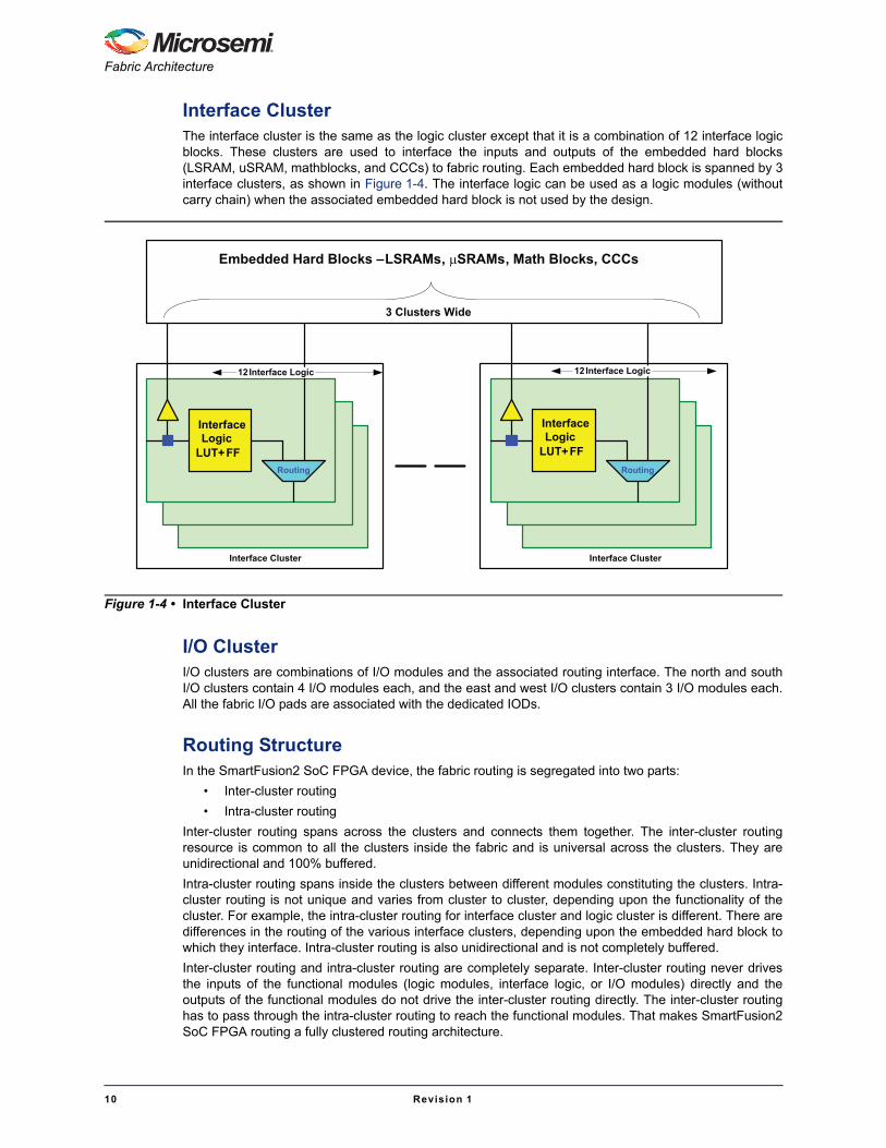
Interface ClusterThe interface cluster is the same as the logic cluster except that it is a combination of 12 interface logicblocks. These clusters are used to interface the inputs and outputs of the embedded hard blocks(LSRAM, uSRAM, mathblocks, and CCCs) to fabric routing. Each embedded hard block is spanned by 3interface clusters, as shown in Figure 1-4. The interface logic can be used as a logic modules (withoutcarry chain) when the associated embedded hard block is not used by the design.
I/O ClusterI/O clusters are combinations of I/O modules and the associated routing interface. The north and southI/O clusters contain 4 I/O modules each, and the east and west I/O clusters contain 3 I/O modules each.All the fabric I/O pads are associated with the dedicated IODs.
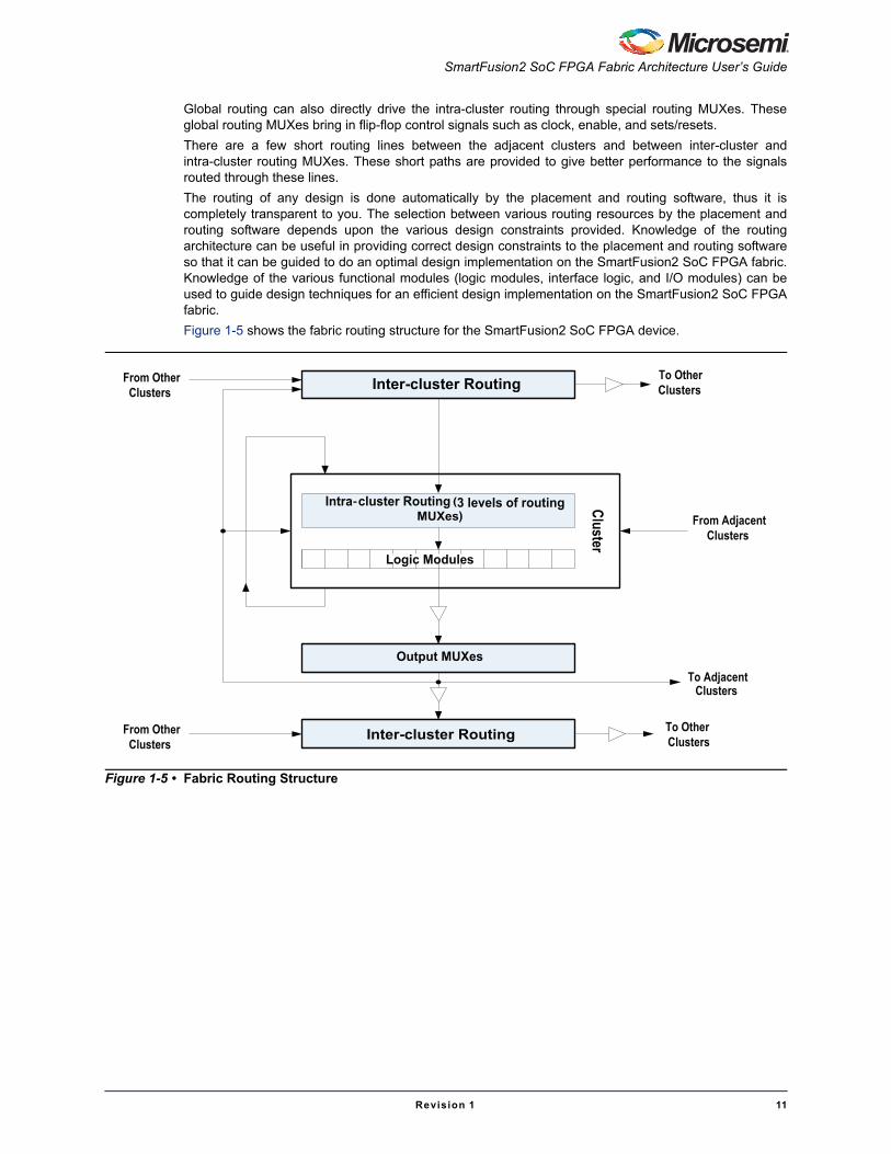
Routing StructureIn the SmartFusion2 SoC FPGA device, the fabric routing is segregated into two parts:
• Inter-cluster routing
• Intra-cluster routing
Inter-cluster routing spans across the clusters and connects them together. The inter-cluster routingresource is common to all the clusters inside the fabric and is universal across the clusters. They areunidirectional and 100% buffered.
Intra-cluster routing spans inside the clusters between different modules constituting the clusters. Intra-cluster routing is not unique and varies from cluster to cluster, depending upon the functionality of thecluster. For example, the intra-cluster routing for interface cluster and logic cluster is different. There aredifferences in the routing of the various interface clusters, depending upon the embedded hard block towhich they interface. Intra-cluster routing is also unidirectional and is not completely buffered.
Inter-cluster routing and intra-cluster routing are completely separate. Inter-cluster routing never drivesthe inputs of the functional modules (logic modules, interface logic, or I/O modules) directly and theoutputs of the functional modules do not drive the inter-cluster routing directly. The inter-cluster routinghas to pass through the intra-cluster routing to reach the functional modules. That makes SmartFusion2SoC FPGA routing a fully clustered routing architecture.
Figure 1-4 • Interface Cluster
Interface Cluster
Routing
Interface Cluster
Embedded Hard Blocks – LSRAMs, μSRAMs, Math Blocks, CCCs
3 Clusters Wide
Interface LogicLUT+FF
Routing
12 Interface Logic
Interface LogicLUT+FF
12 Interface Logic
SmartFusion2 SoC FPGA Fabric Architecture User’s Guide
Revision 1 11
Global routing can also directly drive the intra-cluster routing through special routing MUXes. Theseglobal routing MUXes bring in flip-flop control signals such as clock, enable, and sets/resets.
There are a few short routing lines between the adjacent clusters and between inter-cluster andintra-cluster routing MUXes. These short paths are provided to give better performance to the signalsrouted through these lines.
The routing of any design is done automatically by the placement and routing software, thus it iscompletely transparent to you. The selection between various routing resources by the placement androuting software depends upon the various design constraints provided. Knowledge of the routingarchitecture can be useful in providing correct design constraints to the placement and routing softwareso that it can be guided to do an optimal design implementation on the SmartFusion2 SoC FPGA fabric.Knowledge of the various functional modules (logic modules, interface logic, and I/O modules) can beused to guide design techniques for an efficient design implementation on the SmartFusion2 SoC FPGAfabric.
Figure 1-5 shows the fabric routing structure for the SmartFusion2 SoC FPGA device.
Figure 1-5 • Fabric Routing Structure
Inter-cluster Routing
Inter-cluster Routing
Cluster
Intra-cluster Routing (3 levels of routing MUXes)
Logic Modules
To Other Clusters
From Other Clusters
From Adjacent Clusters
Output MUXesTo Adjacent
Clusters
To Other Clusters
From Other Clusters

Fabric Architecture
12 Revision 1
Fabric Array Coordinate System Every element in the SmartFusion2 SoC FPGA fabric has individual logical X-Y coordinates associatedwith the fabric array coordinate system. These logical coordinates are used by the placement and routingsoftware while implementing the design using fabric elements. You can constrain the placement androuting software to place your design components in specific locations inside the fabric using thiscoordinate system. You can create different types of regions inside the fabric and assign a particular partof the design to that region using the floor-planner software. The boundaries of these regions can bespecified using the array coordinates. Similarly, the embedded hard block is also addressable throughthe fabric coordinate system.
The coordinate system starts from the bottom left corner's logic cell. The X-Y coordinates for thecomplete fabric for M2S050 are shown in Figure 1-6.
Figure 1-6 • M2S050 Fabric Logical Coordinates
887,206
887, 0 0, 0
0,206

SmartFusion2 SoC FPGA Fabric Architecture User’s Guide
Revision 1 13
Glossary
uSRAMMicro static random access memory
CCC Clock conditioning circuits
ClustersClusters are formed by grouping a certain number of logic elements and interconnecting them. This is related to the clustered routing architecture of SmartFusion2 SoC FPGA fabric.
Interface ClusterAn interface cluster is formed by grouping 12 interface logic elements.
I/O ClusterI/O cluster is formed by grouping either 3 or 4 I/O modules.
Interface Logic
The logic element consists of a 4-input LUT and a D flip-flop. This logic element interfaces the hard macros (LSRAMs, uSRAMs, mathblocks) to fabric routing.
I/O Module
The logic element consists of flip-flops and routing MUXs. This logic element interfaces the user I/Os to fabric routing.
Inter-cluster RoutingInter-cluster routing refers to routing resources between various types of clusters.
Intra-cluster RoutingIntra-cluster routing refers to routing resources existing inside a specific cluster.
Logic ClusterA logic cluster is formed by grouping 12 logic modules
Logic ModuleThe basic logic element in SmartFusion2 SoC FPGA fabric, consisting of a 4-input LUT, a D flip-flop and a dedicated carry chain
LSRAMLarge static random access memory

Revision 1 15
2 – LSRAM
This chapter serves as a technical resource to describe the large SRAM (LSRAM) blocks in SmartFusion®2 system-on-chip (SoC) field programmable gate array (FPGA) devices.
IntroductionLSRAMs are big SRAM blocks embedded in the SmartFusion2 SoC FPGA fabric device and are used for storing large data or for creating big FIFOs. These LSRAMs are arranged in multiple rows within the FPGA fabric and can be accessed through the fabric routing architecture. The number of LSRAM blocks available depends upon the specific SmartFusion2 SoC FPGA device selected. For example, in the M2S050 device there are 69 LSRAM blocks available, which are spread across 3 rows inside the fabric.
SmartFusion2 SoC FPGA LSRAM blocks have the following features:
• Each LSRAM block can store up to 18,432 bits of data and can be configured in any of the following depth x width combinations: 512 x 36, 512 x 32, 1k x 18, 1k x 16, 2k x 9, 2k x 8, 4k x 4, 8k x 2, and 16k x 1.
• Each LSRAM block contains two independent data ports – Port A and Port B.
• The LSRAM is synchronous for both read and write operations. These operations are triggered on the rising edge of the clock. The LSRAM can operate at a maximum frequency of 400 MHz.
• The data output ports of the LSRAM have pipeline registers with control signals independent of the LSRAM's control signals. This allows independent control to the pipeline registers. The pipeline registers can be configured as normal registers for Pipelined mode or can be bypassed if not in Pipelined mode.
In Pipelined mode, the input clock sourcing the pipeline registers has to be synchronized to the LSRAM's clock input and should be fed with a single clock source.
• The LSRAM supports two types of read operations: Flow-through read (or non-pipelined) and pipelined read.
– Flow-through read: Flow-through mode indicates a non-pipelined read operation where the pipeline registers are bypassed and the data appears on the corresponding output in the same clock cycle. During Flow-through read operation mode, the LSRAM can generate glitches on the data output buses. Therefore, it is recommended to use the LSRAM with pipeline registers to avoid these read glitches.
– Pipelined read: In a pipelined read operation, the output data is registered at the pipeline registers, so the data appears at the corresponding output in the next clock cycle.
• The LSRAM supports two types of write operations: simple write and feed-through write (or Write bypass mode).
– Simple write: In simple write, the data written into the memory array does not appear on the corresponding data output until it is read out. The data output retains the last read data value.
– Feed-through write (write-bypass write): During this write operation, the data written into the memory array immediately appears on the corresponding data output. The feed-through write option is not supported when the LSRAM is configured in Two-port mode.
• The LSRAM can be operated in two operation modes: Dual-port mode and Two-port mode.
• In Dual-port mode, both the ports are independent; that is, read and write operations can be done from both the ports independently at any location as long as there is no collision. The maximum data-width can be x18 for either port in Dual-port mode. There is no collision detection or prevention circuit built into LSRAM and collision can lead to garbage values being read out or wrong data written into the memory. Therefore, you should avoid collision situations in your design.
LSRAM
16 Revision 1
• In the Two-port mode, Port A is dedicated for read operations and Port B for write operations. In this case, the ports are not independent. In Two-port mode, the maximum data-width for read port (Port A) and write-port (Port B) is x36.
• A write operation requires one clock cycle.
• A read operation requires one clock cycle in Non-pipelined mode. In Pipelined mode, the output data appears in the next cycle.
• If any port is configured with data-widths of x1, x2, or x4, then the other port has to be configured as x1, x2, x4, x8, x16, or x32. This is true for both Dual-port mode and Two-port mode.
Libero® System-on-Chip (SoC) software provides separate configuration tools for Dual-port mode and Two-port mode. You can use them to configure the LSRAM blocks in the required operating modes. These configuration tools generate the required HDL wrapper files for LSRAM with appropriate values assigned to the static signals. You can include these LSRAM wrapper HDL files in the design hierarchy and port map them to the rest of the design. In addition to this, Libero SoC also has the LSRAM macro, RAM1Kx18, which you can directly instantiate in the design. If you are using the RAM1Kx18 macro, you have to provide appropriate values to the static signals to configure the LSRAM correctly before instantiating it in the design.
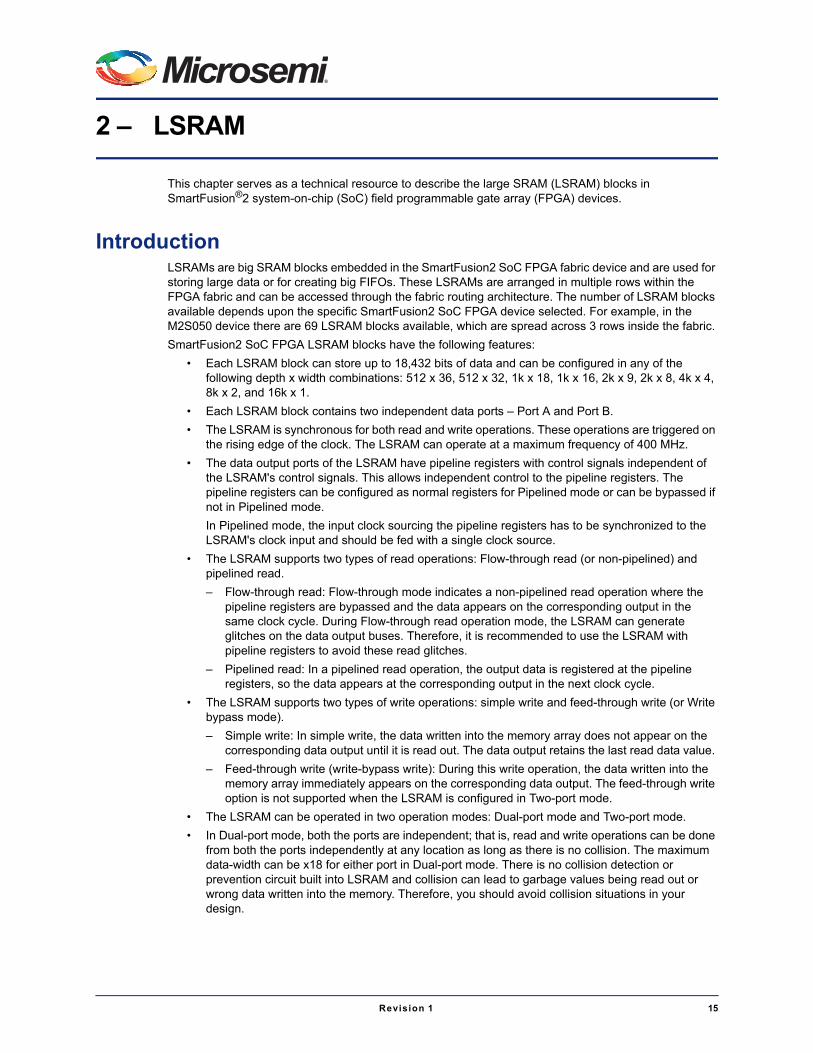
Figure 2-1 shows the simplified top-level functional diagram of the LSRAM. Figure 2-2 shows the LSRAM macro RAM1Kx18 available in Libero SoC.
Figure 2-1 • Simplified Top-Level Functional Block Diagram for LSRAM
A_ DOUT[ 17 : 0 ]
A _DIN[ 17 : 0 ]
B_ DIN [ 17: 0]
A _ ARST_ N
A _ ADDR[ 13: 0 ]
A _ WEN[ 1: 0]
A _BLK[ 2 : 0]
A _CLK
B _ADDR[ 13: 0 ]
B _ WEN[ 1: 0]
B _ BLK[ 2: 0 ]
B _CLK
` B_ARST_ N
Port A Row DecodeWrite Control
Port B Row DecodeWrite Control
Column Decode
Column Decode
B_ DOUT_CLK
A_ DOUT_CLK
B_ DOUT[ 17 : 0 ]
Memory
Array
1 K x 18
Feed-through MUX
Pipeline Register

SmartFusion2 SoC FPGA Fabric Architecture User’s Guide
Revision 1 17
Port List
Figure 2-2 • RAM1Kx18 Macro
Table 2-1 • Port List for LSRAM
Pin Name Pin Direction Type1 Pin name Polarity
PORT A
A_WIDTH[2:0] Input Static Width/depth mode select –
A_WEN[1:0]2 Input Dynamic Write enable High
A_ADDR[13:0] Input Dynamic Address input –
A_DIN[17:0] Input Dynamic Data input –
A_DOUT[17:0] Output Dynamic Data output –
A_BLK[2:0] Input Dynamic Block select High
A_WMODE Input Static Feed-through write select High
A_CLK Input Dynamic Clock Rising
A_ARST_N Input Dynamic Asynchronous reset Low
A_DOUT_CLK Input Dynamic Pipeline register clock Rising
Notes:
1. Static inputs are defined at design time and can be or are controlled by flash configuration bits.
2. If LSRAM is configured in Two-port mode with a write data width of x36/x32 and read data width of x36/x32, both the bits of A_WEN and B_WEN must be tied to logic 1 and should not be dynamically changed.

LSRAM
18 Revision 1
A_DOUT_LAT Input Static Pipeline register Select Low
A_DOUT_ARST_N Input Dynamic Pipeline register asynchronous reset Low
A_DOUT_EN Input Dynamic Pipeline register enable High
A_DOUT_SRST_N Input Dynamic Pipeline register synchronous reset Low
PORT B
B_WIDTH[2:0] Input Static Width/depth mode select –
B_WEN[1:0]2 Input Dynamic Write enable High
B_ADDR[13:0] Input Dynamic Address input –
B_DIN[17:0] Input Dynamic Data input –
B_DOUT[17:0] Output Dynamic Data output –
B_BLK[2:0] Input Dynamic Block select High
B_WMODE Input Static Feed-through write select High
B_CLK Input Dynamic Clock Rising
B_ARST_N Input Dynamic Asynchronous reset Low
B_DOUT_CLK Input Dynamic Pipeline register clock Rising
B_DOUT_LAT Input Static Pipeline register select Low
B_DOUT_ARST_N Input Dynamic Pipeline register asynchronous reset Low
B_DOUT_EN Input Dynamic Pipeline register enable High
B_DOUT_SRST_N Input Dynamic Pipeline register synchronous reset Low
Common Signals
A_EN Input Static Port A power-down Low
B_EN Input Static Port B power-down Low
SII_LOCK Input Static Lock access to SII High
BUSY Output Dynamic Busy signal from SII High
Table 2-1 • Port List for LSRAM (continued)
Pin Name Pin Direction Type1 Pin name Polarity
Notes:
1. Static inputs are defined at design time and can be or are controlled by flash configuration bits.
2. If LSRAM is configured in Two-port mode with a write data width of x36/x32 and read data width of x36/x32, both the bits of A_WEN and B_WEN must be tied to logic 1 and should not be dynamically changed.

SmartFusion2 SoC FPGA Fabric Architecture User’s Guide
Revision 1 19
Port Descriptions
A_WIDTH[2:0] and B_WIDTH[2:0]These are the depth/width mode selections for each port.
A_WEN[1:0] and B_WEN[1:0]These are write enables for each port.
Table 2-2 • Depth/Width Mode Selection
A_WIDTH/B_WIDTH Depth/Width
000 16K x 1
001 8K x 2
010 4k x 4
011 2K x 92K x 8
100 1K x 181K x 16
101110111(Two-port)
512 x 36512 x 32
Table 2-3 • Read/Write Operation Selection
Depth x Width A_WEN/B_WEN Operation
16K x 1
8K x 2
4K x 4
2K x 8
2K x 9
1K x 16
1K x 18
00 Read operation
16K x 1
8K x 2
4K x 4
2K x 8
2K x 9
01 Write operation
1K x 16 11 Write [15:0]
1K x 18 11 Write [15:0]
512 x 32
(Two-port write-Port B)
A_WEN[1:0] = “11”
B_WEN[1:0] = “11”
Write [31:0]
512 x 36
(Two-port write-Port B)
A_WEN[1:0] = “11”
B_WEN[1:0] = “11”
Write [35:0]
Notes:
1. In Dual-port mode, every port reads when the corresponding write enable (A_WEN/B_WEN) is "00" and corresponding port select (A_BLK/B_BLK) is active.
2. In Two-port mode, the read port (Port A) reads in every clock cycle if A_BLK is active.

LSRAM
20 Revision 1
A_ADDR[13:0] and B_ADDR[13:0]These are the address buses for the two ports. Fourteen bits are needed to address the 16,384 independent locations in x1 mode. In wider modes, fewer address bits are used. The needed address bits are most significant bit (MSB) justified and unused least significant bit s (LSBs) have to be grounded.
A_DIN[17:0] and B_DIN[17:0]These are the data input buses for the two ports. In Dual-port mode, the data width can range from 1 bit to 18 bits. In the Two-port mode, Port B becomes the write-only port, A_DIN[17:0] becomes write-data[35:18], and B_DIN[17:0] becomes write-data [17:0], if the write-data width is 36 bits. The needed bits for any mode are LSB justified in the data bus and the unused MSB bits must be grounded.
Table 2-4 • Address Bus Used and Unused Bits
Depth x Width
A_ADDR/B_ADDR
Used Bits Unused bits (to be grounded)
16K x 1 [13:0] None
8K x 2 [13:1] [0]
4K x 4 [13:2] [1:0]
2K x 9
2K x 8
[13:3] [2:0]
1K x 18
1K x 16
[13:4] [3:0]
512 x 36 [13:5] [4:0]
Table 2-5 • Data Input Buses Used and Unused Bits
Depth x Width
A_DIN/B_DIN
Used Bits Unused bits (to be grounded)
16K x 1 [0] [17:1]
8K x 2 [1:0] [17:2]
4K x 4 [3:0] [17:4]
2K x 8 [7:0] [17:8]
2K x 9 [8:0] [17:9]
1K x 16 [16:9] is [15:8]
[7:0] is [7:0]
[17]
[8]
1K x 18 [17:0] None
512 x 32 A_DIN[16:9] is [31:24]
A_DIN[7:0] is [23:16]
B_DIN[16:9] is [15:8]
B_DIN[7:0] is [7:0]
A_DIN[17]
A_DIN[8]
B_DIN[17]
B_DIN[8]
512 x 36 A_DIN[17:0] is [35:18]
B_DIN[17:0] is [17:0]
None

SmartFusion2 SoC FPGA Fabric Architecture User’s Guide
Revision 1 21
A_DOUT[17:0] and B_DOUT[17:0]These are the data output buses for the two ports. In Dual-port mode, the data width can range from 1 bit to 18 bits. In Two-port mode, Port A becomes the read-only port, A_DOUT[17:0] becomes read-data[35:18], and B_DOUT[17:0] becomes read-data [17:0], if the read-data width is 36 bits. The needed bits for any mode are LSB justified in the data bus.
A_BLK[2:0] and B_BLK[2:0]These are port select control signals for each port.
Table 2-6 • Data Output Buses Used and Unused Bits
Depth x WidthA_DOUT/B_DOUT
Used Bits Unused bits (to be grounded)
16K x 1 [0] [17:1]
8K x 2 [1:0] [17:2]
4K x 4 [3:0] [17:4]
2K x 8 [7:0] [17:8]
2K x 9 [8:0] [17:9]
1K x 16 [16:9] is [15:8]
[7:0] is [7:0]
[17]
[8]
1K x 18 [17:0] None
512 x 32 B_DOUT[16:9] is [31:24]
B_DOUT[7:0] is [23:16]
A_DOUT[16:9] is [15:8]
A_DOUT[7:0] is [7:0]
B_DOUT[17]
B_DOUT[8]
A_DOUT[17]
A_DOUT[8]
512 x 36 A_DOUT[17:0] is [35:18]
B_DOUT[17:0] is [17:0]
None
Table 2-7 • Port Select Control Signals
Port Select Signal Value Result
A_BLK[2:0] 111 Perform read or write operation on Port A.
A_BLK[2:0] 000
001
010
011
100
101
110
No operation in memory from Port A. Port A output is forced to logic 0.
B_BLK[2:0] 111 Perform read or write operation on Port A.
B_BLK[2:0] 000
001
010
011
100
101
110
No operation in memory from Port B. Port B output is forced to logic 0.

LSRAM
22 Revision 1
Table 2-8 • Other LSRAM Input/Output Signals
Port Name Direction Description
A_WMODE, B_WMODE
Input These signals represent the Write mode control signals for Port A and Port B.
Logic 0: Output data port holds the previous value.
Logic 1: Feed-through; write data appears on the corresponding output data port. In Two-port mode, feed-through write is not supported.
A_CLK, B_CLK Input These signals represent the clock inputs for Port A and Port B. You must set up all inputs before the rising edge of the clock. The read or write operation begins with the rising edge.
A_ARST_N, B_ARST_N
Input These signals represent active low, asynchronous reset inputs for Port A and Port B. Assertion of these resets during read operation will force the data output lines to logic 0. Assertion of these resets during write operation will result in garbage values written into the memory.
A_DOUT_LAT, B_DOUT_LAT
Input These signals represent Latch mode inputs for the output pipeline registers for Port A and Port B.
Logic 0: Register operation
Logic 1: Latch operation
A_DOUT_ARST_N, B_DOUT_ARST_N
Input These signals represent active low, asynchronous reset inputs for the output pipeline registers for Port A and Port B. Assertion of these reset signals forces the data output to logic 0. In Non-pipelined mode, these inputs should be tied to logic 1.
A_DOUT_EN, B_DOUT_EN
Input These signals represent active high, enable inputs for the output pipeline registers for Port A and Port B.
Logic 0: Normal register operation
Logic 1: Register holds previous data
A_DOUT_SRST_N, B_DOUT_SRST_N
Input These signals represent active low, synchronous reset inputs for the output pipeline registers for Port A and Port B. Assertion of these reset signals forces the data output to logic 0. In Non-pipelined mode, these inputs should be tied to logic 1.
A_EN, B_EN Input These are active low, power-down configuration bits for each port.
SII_LOCK Input This control signal, when logic 1, locks the entire LSRAM memory for being accessed by the system controller interface bus (SII). The system controller can access the LSRAM for various purposes such as testing the memory, moving data between LSRAM and eNVM or external memories, or movement of data between various LSRAMs or between uSRAMs and LSRAMs. You cannot access the LSRAMs when the system controller is accessing them.
BUSY Output This signal acts as a status signal when the system controller is accessing the particular LSRAM. Logic 1 on this signal indicates system controller access. You can monitor this signal to know when the system controller has completed its access for the particular LSRAM.

SmartFusion2 SoC FPGA Fabric Architecture User’s Guide
Revision 1 23
Operating ModesLSRAM can be configured as a dual-port SRAM or two-port SRAM.
Dual-Port ModeLSRAM configured as dual-port SRAM provides a data storage capability of 18 Kb with two independent access ports: Port A and Port B. The maximum data width can be x18 for either port in Dual-port mode. In Dual-port mode, each port of the LSRAM can be configured in the following depth x width configurations:
• 1k x 18, 1k x 16
• 2k x 9, 2k x 8
• 4k x 4
• 8k x 2
• 16k x 1
Data can be written to either or both ports and also can be read from either or both ports. Each port has its own address, data in, data out, clock, clock enable, and write enable. The read and write operations are synchronous and require a clock edge.
There is no collision detection or prevention circuit built into LSRAM. Simultaneous write operations from both the ports to the same address location result in data uncertainty. Simultaneous read and write operations from both the ports to the same address location results in correct data written into the memory but garbage values being read out. You should avoid generating collision situations in the designs.
The read operation requires one clock cycle in Non-pipelined mode. In Pipelined mode, the output data appears in the next cycle. The write operation requires one clock cycle.
When the read operation is configured with output pipeline registers, the input clock sourcing the pipeline registers has to be synchronized to the LSRAM's clock input; that is, A_DOUT_CLK should be synchronized to A_CLK and B_DOUT_CLK should be synchronized to B_CLK.
Table 2-9 shows the data width configurations that are supported by LSRAM configured in Dual-port mode.
Table 2-9 • Data Width Configurations for LSRAM in Dual-Port Mode
Port A Data Width (represented as “x number of bits”) Port B Data Width (represented as “x number of bits”)
x1 x1, x2, x4, x8, x16
x2 x1, x2, x4, x8, x16
x4 x1, x2, x4, x8, x16
x9 x9, x18
x18 x9, x18
LSRAM
24 Revision 1
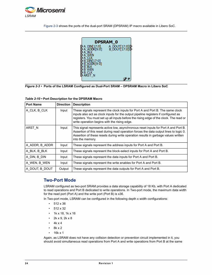
Figure 2-3 shows the ports of the dual-port SRAM (DPSRAM) IP macro available in Libero SoC.
Two-Port ModeLSRAM configured as two-port SRAM provides a data storage capability of 18 Kb, with Port A dedicated to read operations and Port B dedicated to write operations. In Two-port mode, the maximum data width for the read port (Port A) and the write port (Port B) is x36.
In Two-port mode, LSRAM can be configured in the following depth x width configurations:
• 512 x 36
• 512 x 32
• 1k x 18, 1k x 16
• 2k x 9, 2k x 8
• 4k x 4
• 8k x 2
• 16k x 1
Again, as LSRAM does not have any collision detection or prevention circuit implemented in it, you should avoid simultaneous read operations from Port A and write operations from Port B at the same
Figure 2-3 • Ports of the LSRAM Configured as Dual-Port SRAM – DPSRAM Macro in Libero SoC
Table 2-10 • Port Description for the DPSRAM Macro
Port Name Direction Description
A_CLK, B_CLK Input These signals represent the clock inputs for Port A and Port B. The same clock inputs also act as clock inputs for the output pipeline registers if configured as registers. You must set up all inputs before the rising edge of the clock. The read or write operation begins with the rising edge.
ARST_N Input This signal represents active low, asynchronous reset inputs for Port A and Port B. Assertion of this reset during read operation forces the data output lines to logic 0. Assertion of these resets during write operation results in garbage values written into the memory.
A_ADDR, B_ADDR Input These signals represent the address inputs for Port A and Port B.
A_BLK, B_BLK Input These signals represent the block-select inputs for Port A and Port B.
A_DIN, B_DIN Input These signals represent the data inputs for Port A and Port B.
A_WEN, B_WEN Input These signals represent the write enables for Port A and Port B.
A_DOUT, B_DOUT Output These signals represent the data outputs for Port A and Port B.

SmartFusion2 SoC FPGA Fabric Architecture User’s Guide
Revision 1 25
address location. This situation results in correct values being written into the memory, but garbage values will be read out from the memory.
When the read port data width is configured as x36/x32, output data pins are borrowed from Port B, with Port A forming the MSB and Port B forming the LSB.
When the write port data width is configured as x36/x32, input data pins are borrowed from Port A, with Port A forming the MSB and Port B forming the LSB.
The read operation requires one clock cycle in Non-pipelined mode. In Pipelined mode, the output data appears in the next cycle. The write operation requires one clock cycle.
When the read operation is configured with output pipeline registers, the input clock sourcing the pipeline registers has to be synchronized to the LSRAM's clock input. When the read data width is x18 or less, A_DOUT_CLK has to be synchronized to A_CLK. When the read data width is x36/x32, both A_DOUT_CLK and B_DOUT_CLK have to be synchronized to A_CLK.
Table 2-11 shows the data width configurations supported by LSRAM configured in Two-port mode.
LSRAM does not support any two-port configurations with a write port (Port B) data width of x36/x32 and a read port (Port B) data width of x18/x9/x8/x4/x2/x1. If you desire to have such a configuration for the design, you will have to use two LSRAM blocks to implement these configurations. Following is a use case which explains how you can implement a two-port SRAM (using RAM1kx18 macros) with a write data width of x36 and a read data width of x18.
The implementation has following configuration:
• Write port: 512 x36
• Read port: 1024 x18
• Read and write input clock: 2 different clock sources
• Pipelined read mode: disabled
Table 2-11 • Data Width Configurations for LSRAM in Two-Port Mode
Read Port – Port A (represented as “x number of bits”)
Write Port – Port B (represented as “x number of bits”)
x1 x1, x2, x4, x8, x16
x2 x1, x2, x4, x8, x16
x4 x1, x2, x4, x8, x16
x8 x1, x2, x4, x8, x16
x9 x9, x18
x16 x1, x2, x4, x8, x16
x18 x9, x18
x32 x1, x2, x4, x8, x16, x32
x36 x9, x18, x36
Note: In Two-port mode, if the write data width is x36/x32 and read data width is x36/x32, both the bits of A_WEN andB_WEN have to be tied to logic 1 and should not be dynamically changed.
LSRAM
26 Revision 1
Figure 2-4 shows the two-port SRAM with a write data width of x36 and read data width of x18.
Figure 2-4 • Two-Port SRAM With W36 and R18
A_CLKA_ARST_NA_BLK[2:0]A_ADDR[13:0]A_DIN[17:0]A_WEN[1:0]A_DOUT_ENA_DOUT_ARST_NA_DOUT_SRST_N
B_CLKB_ARST_NB_BLK[2:0]B_ADDR[13:0]B_DIN[17:0]B_WEN[1:0]B_DOUT_ENB_DOUT_ARST_NB_DOUT_SRST_N
A_DOUT_LATA_WIDTH[2:0]A_WMODEA_EN
B_DOUT_LATB_WIDTH[2:0]B_WMODEB_ENS_LOCK
A_DOUT[17:0]
B_DOUT[17:0]
BUSY
A_CLKA_ARST_NA_BLK[2:0]A_ADDR[13:0]A_DIN[17:0]A_WEN[1:0]A_DOUT_ENA_DOUT_ARST_NA_DOUT_SRST_N
B_CLKB_ARST_NB_BLK[2:0]B_ADDR[13:0]B_DIN[17:0]B_WEN[1:0]B_DOUT_ENB_DOUT_ARST_NB_DOUT_SRST_N
A_DOUT_LATA_WIDTH[2:0]A_WMODEA_EN
B_DOUT_LATB_WIDTH[2:0]B_WMODEB_EN
S_LOCK
A_DOUT[17:0]
B_DOUT[17:0]
BUSY
LSRAM #1
LSRAM #2
RCLK‘1’
REN,’1',’1'‘0’,RADDR[9:0],‘0’,’0',’0'
18'b0“00”
‘1’ARST_N
‘1’
WCLK
A_DOUT_CLK‘1’
B_DOUT_CLK
A_DOUT_CLK‘1’
B_DOUT_CLK
‘1’WEN,’1',’1'
‘0’,WADDR[8:0],’0',‘0’,’0',’0'WD[26:19], WD[8:0]
3
14
3
14
“11”18‘1’‘0’‘1’‘1’
‘1’“011”
‘0’‘1’
‘1’“100”
‘0’‘1’‘0’
‘1’
18'b0“00”
‘1’
‘1’
‘1’
WD[35:27], WD[17:9]“11”
‘1’‘0’‘1’‘1’
‘1’“011”
‘0’‘1’
‘1’“100”
‘0’‘1’
‘0’
RD[17:9]
Not Connected
Not Connected
RD[8:0]
Not Connected
Not Connected

SmartFusion2 SoC FPGA Fabric Architecture User’s Guide
Revision 1 27
However, the two-port LSRAM software configurator (TPSRAM) available in Libero SoC can do the above implementation automatically if you configure it with any of the data width configurations shown in Table 2-12.
Figure 2-5 shows the ports of the TPSRAM IP macro available in Libero SoC.
Table 2-12 • Two-Port Configurations Requiring 2 LSRAM Blocks
Write Data Width Read Data Width
W36 W18
W32 W16
W36 W9
W32 W8
W32 W4
W32 W2
W32 W1
Figure 2-5 • Ports of the LSRAM Configured as Two-Port SRAM – TPSRAM Macro in Libero SoC
Table 2-13 • Port Description for the TPSRAM Macro
Port Name Direction Description
WCLK Input This signal represents the clock input for the write port (Port B). You must set up all write inputs before the rising edge of the clock. The write operation begins with the rising edge.
RCLK Input This signal represents the clock input for the read port (Port A). The same clock inputs also act as clock inputs for the output pipeline registers if configured as registers. You must set up all read inputs before the rising edge of the clock. The read operation begins with the rising edge.
ARST_N Input This signal represents active low, asynchronous reset inputs for Port A and Port B. Assertion of this reset during read operation forces the data output lines to logic ‘0’. Assertion of these resets during write operation results in garbage values written into the memory.
WADDR Input This signal represents the address input for write Port B.
RADDR Input This signal represents the address input for read Port A.
WEN Input This signal represents the write enable for write Port B.
WD Input This signal represents the data input for write Port B.
REN Input This signal represents the read enable for read Port A.
RD Output This signal represents the data output for read Port A.

LSRAM
28 Revision 1
Timing Diagrams
Simple Read Timing • The addresses (A_ADDR, B_ADDR), BLK enables (A_BLK, B_BLK), and read enables (A_WEN,
B_WEN = '0') should be set up before the rising edge of the clock (A_CLK, B_CLK).
• For non-pipeline read operations, data comes on the output bus (A_DOUT, B_DOUT) after a delay of tcdout in the same cycle.
• For pipeline read operations, the data appears on the output in the next clock cycle.
• LSRAM can generate glitches on the data output port if the pipeline registers are not used. The pipeline registers do not allow these glitches to pass on to the data output port. Microsemi recommends that you use Pipeline read operation mode.
Figure 2-6 shows the timing diagram for a simple read operation performed on LSRAM.
Figure 2-6 • Read Operation Timing Waveforms
taddrsu taddrhd
tblksu tblkhd
trdesu trdehd
tcy
tch tcl
tclk2q
tclk2q
A_ CLKB_ CLK
A_ ADDR [13 :0 ]B_ ADDR [13 :0 ]
A_ BLK [2 :0 ]B_ BLK [2 :0 ]
A _ WENB _ WEN
A_DOUT [17 :0 ] ( non pipeline read )B_ DOUT [17 :0 ] ( non pipeline read )
A_DOUT [17 :0 ] ( pipeline read )B_ DOUT [17 :0 ] ( pipeline read )

SmartFusion2 SoC FPGA Fabric Architecture User’s Guide
Revision 1 29
Simple Write and Feed-Through Write Timing• The addresses (A_ADDR, B_ADDR), BLK enables (A_BLK, B_BLK), and write enables (A_WEN,
B_WEN = '1') should be set up before the rising edge of the clock (A_CLK, B_CLK).
• For a feed-through write, the written data appears on the output (A_DOUT, B_DOUT) after adelay of tcdout in the same clock cycle.
• For a simple write, the written data appears on the output only when a read operation isperformed on the same address.
Table 2-14 • Read Operation Timing Parameters
Parameters Comments
tcy Clock period
tch Clock Minimum Pulse Width High
tcl Clock Minimum pulse Width Low
taddrsu Address Setup Time
taddrhd Address Hold Time
tblksu Block Select Setup Time (With Pipeline Register Enabled)
tblkhd Block Select Hold Time (With Pipeline Register Enabled)
trdesu Read Enable Setup Time (A_WEN, B_WEN =0)
trdehd Read Enable Hold Time (A_WEN, B_WEN =0)
tclk2qRead Access Time with Pipeline Register
Read Access Time without Pipeline Register

LSRAM
30 Revision 1
Figure 2-7 shows the timing diagram for a simple write operation performed on LSRAM.
Figure 2-7 • Write Operation Timing Waveforms
taddrsu taddrhd
tblksu tblkhd
twesu twehd
tcy
tch tcl
tclk2q
A _ CLKB _ CLK
A _ AADR [13 :0 ]
B _ ADDR[13 :0 ]
A _ BLK [2 :0 ]B _ BLK [2 :0 ]
A _ WENB _ WEN
A_ DOUT [17 :0 ] ( feed - through )B_DOUT [17 :0 ] ( feed - through )
tdsu tdhd
A _ DIN [17 :0 ]
B _DIN [17 :0 ]
Table 2-15 • Write Operation Timing Parameters
Parameters Comments
tcy Clock period
tch Clock Minimum Pulse Width High
tcl Clock Minimum pulse Width Low
taddrsu Address Setup Time
taddrhd Address Hold Time
tblksu Block Select Setup Time (With Pipeline Register Enabled)
tblkhd Block Select Hold Time (With Pipeline Register Enabled)
twesu Write Enable Setup Time (A_WEN, B_WEN =1)
twehd Write Enable Hold Time (A_WEN, B_WEN =1)
tdsu Data Setup Time
tdhd Data Setup Time
tclk2q Read Access Time with Feed-through write timing

SmartFusion2 SoC FPGA Fabric Architecture User’s Guide
Revision 1 31
Block Select TimingThe block select in LSRAM works like a chip select. When the block select (A_BLK and B_BLK) is High, the LSRAM is active and read and write operations can be performed on it.
If the block select is Low, the LSRAM does not perform any read or write operations. It will drive logic 0 on the data output pins until the next read cycle or write operation in Bypass mode. When the pipeline registers are used, the block select effect at the outputs is delayed by one pipeline clock cycle (the pipeline registers are independent of block select).
Figure 2-8 shows the timing diagram for block select inputs for LSRAM.
Figure 2-8 • Block Select Timings
tcy
A_ CLKB_ CLK
A_ BLK [2 :0 ]B_ BLK [2 :0 ]
tblksu tblkhd
A_DOUT [17:0] (non pipeline mode )B_DOUT [17:0] (non pipeline mode )
tclk 2q
A_DOUT [17:0] (pipeline access)B_DOUT [17:0] (pipeline access)
tblk 2q
tblkmpw
Table 2-16 • Block Selection Timing Parameters
Parameters Comments
tcy Clock period
tch Clock Minimum Pulse Width High
tcl Clock Minimum pulse Width Low
tblksu Block Select Setup Time (With Pipeline Register Enabled)
tblkhd Block Select Hold Time (With Pipeline Register Enabled)
tblkmpw Block Select Minimum Pulse Width

LSRAM
32 Revision 1
Reset OperationThe reset signals (A_ARST_N and B_ARST_N) are asynchronous active low signals. For any normal operation of LSRAM, these reset signals should be kept High. To reset the LSRAM, these reset signals should be made Low.
When reset is asserted (A_ARST_N or B_ARST_N forced low), the LSRAM behaves as follows during read and write operations:
1. Read operation: If reset is asserted when the read operation is in process, the data output port is forced Low after a certain amount of delay. If the clock is High and the reset signal is asserted and then deasserted in the same High clock phase or Low clock phase, the data output stays Low until the next cycle. The data output changes its state only if a read operation or write operation in Bypass mode is performed on the LSRAM. In a simple write operation, the data output will stay Low.
2. Write operation: The corrupted data is written into the memory. To avoid data corruption, it is recommended that you avoid asserting reset during write operation.
CollisionCollision scenarios arise between both the ports of the LSRAM when a read operation is requested from one port and a write operation from the other port simultaneously on the same address location, or when a write operation occurs at the same location at the same time from both the ports. Table 2-17 describes the behavior of the LSRAM during the various cases of collisions.
Note: The last 3 scenarios mentioned in Table 2-17 are not allowed on LSRAM and should be avoided. There are no collision prevention or detection techniques implemented in LSRAM.
tblk2qBlock Select to Out Disable/Enable Time (when Pipeline Registers are disabled)
tclk2q Read Access Time without Pipeline Register
Table 2-16 • Block Selection Timing Parameters (continued)
Table 2-17 • Collision Operation Description
Operation Description
Simultaneous read from Port A and Port B at the same location
Operation allowed without any restrictions and data is available on the output ports after the specified time, as described in the read timing diagrams in Figure 2-5 on page 27.
Simultaneous read from Port A and write from Port B at the same location
Not allowed. The new data may be written into the address location but the read data out will be a garbage value.
Simultaneous read from Port B and write from Port A at the same location
Not allowed. The new data may be written into the address location but the read data out will be a garbage value.
Simultaneous write from Port A and Port B at the same location
Not allowed. If the data to be written is the same on both the ports, then data is successfully written. But if the data is different, then the LSRAM cell will have an undetermined state.

SmartFusion2 SoC FPGA Fabric Architecture User’s Guide
Revision 1 33
Glossary
Acronyms
LSBLeast significant bit
LSRAMLarge static random access memory
MSBMost significant bit
uSRAMMicro static random access memory
Terminology
Flow-through ReadA read operation performed with the output not being registered by the output pipeline registers.
Pipelined ReadA read operation performed with the output being registered by the output pipeline registers.
Simple WriteA write operation in which the data written does not appear on the SRAM output ports.
Feed-through Write (Write-Bypass Write)A write operation in which the data written appears on the SRAM output ports immediately.
Dual-Port ModeSRAM with two independent ports through which both read and write operation can be done.
Two-Port ModeSRAM with two ports, one dedicated to read operations and the other dedicated to write operations.
List of ChangesThe following table lists critical changes that were made in each revision.
Date Changes Page
50200329-1/10.12 Added new Figure 2-6, Figure 2-7, and Figure 2-8 28, 30, and 31
Updated Table 2-14, Table 2-15, and Table 2-16 29, 30, and 31


Revision 1 35
3 – Micro SRAM (uSRAM)
This chapter describes the Micro SRAM (uSRAM) blocks in SmartFusion®2 system-on-chip (SoC) field programmable gate array (FPGA) devices.
IntroductionuSRAMs are small SRAM blocks embedded in the fabric of the SmartFusion2 SoC FPGA device, in contrast to large SRAM (LSRAM) blocks. These uSRAM blocks are basically used for data storage, buffering, and creating embedded FIFOs that can be used by any embedded fabric master. uSRAMs are arranged in multiple rows within the FPGA fabric and can be accessed through the fabric routing architecture. The number of uSRAM blocks available depends upon the specific SmartFusion2 SoC FPGA device selected; for example, in the M2S050T SmartFusion2 SoC FPGA device, there are 72 uSRAM blocks available, which are spread across 3 rows inside the fabric.
SmartFusion2 SoC FPGA uSRAM blocks have the following features:
• Each uSRAM block can store up to 1 Kb (1152 bits) of data and can be configured in any of the following depth x width combinations: 64 x 18, 64 x 16, 128 x 9, 128 x 8, 256 x 4, 512 x 2, and 1024 x 1.
• Each uSRAM has 2 read ports (Port A and Port B) and 1 Write port (Port C).
• The read operations can be performed in both Synchronous and Asynchronous modes. The write operation can be done only in Synchronous mode.
• The two read ports have registers on their address and block select input lines for enabling Synchronous mode operation. These registers can also be configured as transparent latches for Asynchronous mode operations.
• The two read ports also have output registers for Pipelined mode which are clocked by a different clock input. Output pipeline registers can be configured as normal registers or as latches or can be made completely transparent. When the pipeline registers are configured as registers or latches, the clock input controls the input to output path of the pipeline registers. When the pipeline registers are configured as fully transparent, the clock input is tied High.
However, when the input address / block select registers and the output pipeline registers are configured as normal registers, the clock inputs of both the input and output registers should be synchronous to each other and should be fed with a single clock source. In software, these clock inputs are shown as two different signals so that you can tie them off individually when any of the registers must be configured as a transparent latch.
Microsemi recommends that you configure the pipeline registers in either the register or latch mode during read operation to avoid glitches on the read output data lines.
• Due to the availability of separate input address and output pipeline registers, the read operations through Port A and Port B in uSRAM can be performed in six different modes:
– Synchronous read mode without pipeline registers (Synchronous-Asynchronous mode)
– Synchronous read mode with pipeline registers (Synchronous-Synchronous mode)
– Asynchronous read mode without pipeline registers (Asynchronous-Asynchronous mode)
– Asynchronous read mode with pipeline registers (Asynchronous-Synchronous mode)
– Synchronous read mode with pipeline registers configured as latches
– Asynchronous read mode with pipeline registers configured as latches
• Separate synchronous and asynchronous resets are provided for the input address / block select registers. Assertion of the resets when these input registers are configured as registers forces the address and block select register values to logic 0, which subsequently forces the output data lines to logic 0. These resets can be used to initialize the read ports.

Micro SRAM (uSRAM)
36 Revision 1
• The output pipeline registers have separate synchronous and asynchronous resets which provide independent control to these registers. When asserted, the data output lines are forced to logic 0.
• Both the input and output registers of the read ports have enable inputs. When logic 0 is applied to these enable inputs, the input registers hold the previous address and the output pipeline registers hold the previous read data out.
• The uSRAM can operate at up to 400 MHz in Synchronous-Synchronous read mode through Port A and Port B, including a write at 400 MHz through Port C.
• The two read ports are independent of each other and simultaneous read operations can be performed from both ports at the same address location.
Simultaneous read and write operations at the same location are not allowed because they would result in a successful write operation but ambiguous read data. There is no collision prevention or detection implemented in uSRAM. You should avoid simultaneous read and write operations at the same address location in designs.
Libero® System-on-Chip (SoC) software provides configuration tools which can be used to configure uSRAM blocks. These configuration tools generate the required HDL wrapper files for uSRAM with appropriate values assigned to the static signals. You can include these uSRAM wrapper HDL files in the design hierarchy and port map them to the rest of the design. In addition, Libero SoC also has the uSRAM macro RAM64x18, which you can directly instantiate in the designs. If you are using the RAM64x18 macro, you must provide appropriate values to the static signals to configure the uSRAM in the correct configuration before instantiating it in the design.
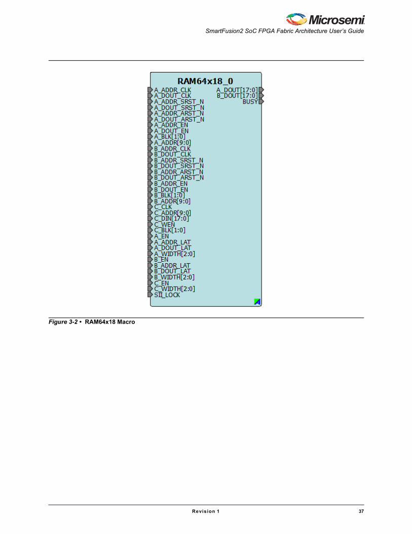
Figure 3-1 shows a top-level functional diagram of the uSRAM block. Figure 3-2 on page 37 shows the uSRAM RAM64x18 macro available in Libero SoC. Table 3-1 on page 38 shows the port list.
Figure 3-1 • Simplified Functional Block Diagram of uSRAM
A_DOUT[17:0]Port ARead
Decode
Port BRead
Decode
B_DOUT_CLK
A_DOUT_CLK
B_DOUT[17:0]
Memory Array
64 x 18
C_ADDR9:0]
C_DIN[17:0]
C_WEN
C_CLK
Port
Cw
rite
cont
rol
A_ADDR[9:0]A_BLK[1:0]
A_ADDR_CLK
B_ADDR[9:0]B_BLK[1:0]
B_ADDR_CLK
Pipeline Registers
SmartFusion2 SoC FPGA Fabric Architecture User’s Guide
Revision 1 37
Figure 3-2 • RAM64x18 Macro

Micro SRAM (uSRAM)
38 Revision 1
Port ListTable 3-1 • Port List for uSRAM
Pin Name Direction Type* Descriptions Polarity
Port A
A_ADDR[9:0] Input Dynamic Address input –
A_BLK[1:0] Input Dynamic Block select Active high
A_WIDTH[2:0] Input Static Depth x width mode selection –
A_DOUT[17:0] Output Dynamic Data output –
A_DOUT_ARST_N Input Dynamic Pipeline register asynchronous reset Active low
A_DOUT_CLK Input Dynamic Pipeline register clock input Rising
A_DOUT_EN Input Dynamic Pipeline register enable Active low
A_DOUT_LAT Input Static Pipeline Latch mode input Active high
A_DOUT_SRST_N Input Dynamic Pipeline register synchronous reset Active low
A_ADDR_CLK Input Dynamic Address register clock Rising
A_ADDR_EN Input Dynamic Address register enable Active high
A_ADDR_LAT Input Static Address register Latch mode input Active high
A_ADDR_SRST_N Input Dynamic Address register synchronous reset Active low
A_ADDR_ARST_N Input Dynamic Address register asynchronous reset Active low
Port B
B_ADDR[9:0] Input Dynamic Address input
B_BLK[1:0] Input Dynamic Block select Active high
B_WIDTH[2:0] Input Static Depth x width mode selection –
B_DOUT[17:0] Output Dynamic Data output –
B_DOUT_ARST_N Input Dynamic Pipeline register Asynchronous reset Active Low
B_DOUT_CLK Input Dynamic Pipeline register clock input Rising
B_DOUT_EN Input Dynamic Pipeline register enable Active Low
B_DOUT_LAT Input Static Pipeline Latch mode input Active high
B_DOUT_SRST_N Input Dynamic Pipeline register synchronous reset Active low
B_ADDR_CLK Input Dynamic Address register clock Rising
B_ADDR_EN Input Dynamic Address register enable Active high
B_ADDR_LAT Input Static Address register Latch mode input Active high
B_ADDR_SRST_N Input Dynamic Address register synchronous reset Active low
B_ADDR_ARST_N Input Dynamic Address register asynchronous reset Active low
Note: *Static inputs are defined at design time and are controlled by flash configuration bits.
SmartFusion2 SoC FPGA Fabric Architecture User’s Guide
Revision 1 39
Port Description
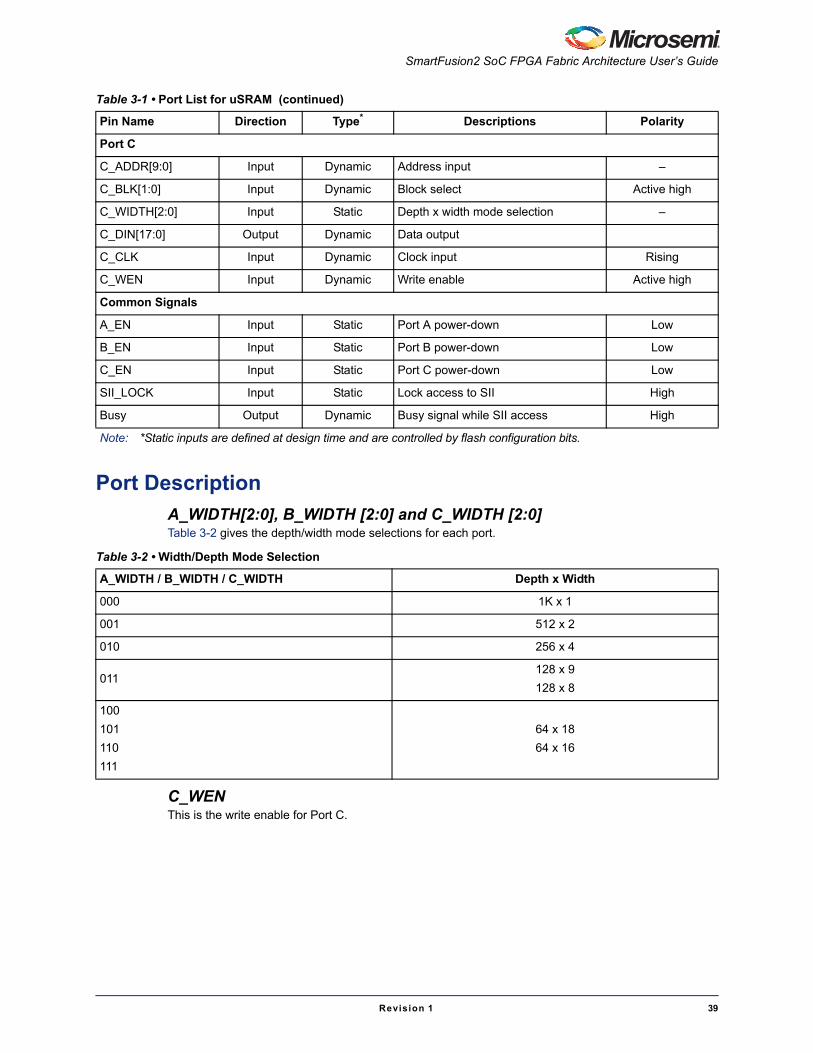
A_WIDTH[2:0], B_WIDTH [2:0] and C_WIDTH [2:0]Table 3-2 gives the depth/width mode selections for each port.
C_WENThis is the write enable for Port C.
Port C
C_ADDR[9:0] Input Dynamic Address input –
C_BLK[1:0] Input Dynamic Block select Active high
C_WIDTH[2:0] Input Static Depth x width mode selection –
C_DIN[17:0] Output Dynamic Data output
C_CLK Input Dynamic Clock input Rising
C_WEN Input Dynamic Write enable Active high
Common Signals
A_EN Input Static Port A power-down Low
B_EN Input Static Port B power-down Low
C_EN Input Static Port C power-down Low
SII_LOCK Input Static Lock access to SII High
Busy Output Dynamic Busy signal while SII access High
Table 3-1 • Port List for uSRAM (continued)
Pin Name Direction Type* Descriptions Polarity
Note: *Static inputs are defined at design time and are controlled by flash configuration bits.
Table 3-2 • Width/Depth Mode Selection
A_WIDTH / B_WIDTH / C_WIDTH Depth x Width
000 1K x 1
001 512 x 2
010 256 x 4
011128 x 9
128 x 8
100
101
110
111
64 x 18
64 x 16

Micro SRAM (uSRAM)
40 Revision 1
A_ADDR[9:0], B_ADDR [9:0] and C_ADDR [9:0]Table 3-3 shows the address buses for the three ports (two read and one write). Ten bits are needed to address the 1,152 independent locations in x1 mode. In wider configurations, fewer address bits are used; the details of unused bits are shown in Table 3-3. The needed address bits are most significant bit (MSB) justified and unused least significant bit (LSB) bits must be grounded.
C_DIN[17:0]Table 3-4 describes the data input bus for write Port C. The required bits for all modes are LSB justified in the data bus and the unused MSB bits need to be grounded.
Table 3-3 • Address Bus Used and Unused Bits
Depth x WidthA_ADDR / B_ADDR / C_ADDR
Used Bits Unused Bits (to be grounded)
1K x 1 [9:0] None
512 x 2 [9:1] [0]
256 x 4 [9:2] [1:0]
128 x 9
128 x 8[9:3] [2:0]
64 x 18
64 x 16[9:4] [3:0]
Table 3-4 • Data Input Buses Used and Unused Bits
Depth x WidthC_DIN
Used Bits Unused Bits (to be grounded)
1K x 1 [0] [17:1]
512 x 2 [1:0] [17:2]
256 x 4 [3:0] [17:4]
128 x 8 [7:0] [17:8]
128 x 9 [8:0] [17:9]
64 x 16[16:9]
[7:0]
[17]
[8]
64 x 18 [17:0] None

SmartFusion2 SoC FPGA Fabric Architecture User’s Guide
Revision 1 41
A_DOUT[17:0] and B_DOUT[17:0]Table 3-5 describes the data output buses for Port A and Port B. The required bits for any mode are LSB justified in the data bus.
A_BLK[1:0], B_BLK [1:0] and C_BLK [1:0]Table 3-6 describes the port select control signals for Port A, Port B, and Port C.
Table 3-5 • Data Output Buses Used and Unused Bits
Depth x WidthA_DOUT/B_DOUT
Used Bits Unused Bits
1K x 1 [0] [17:1]
512 x 2 [1:0] [17:2]
256 x 4 [3:0] [17:4]
128 x 8 [7:0] [17:8]
128 x 9 [8:0] [17:9]
64 x 16[16:9]
[7:0]
[17]
[8]
64 x 18 [17:0] None
Table 3-6 • Port Select Control Signals
Port Select Signal Value Operation
A_BLK[1:0]
11 Perform read operation on Port A.
00
01
10
Port A is not selected and its read data will be logic 0.
B_BLK[1:0]
11 Perform read operation on Port B.
00
01
10
Port B is not selected and its read data will be logic 0.
C_BLK[1:0]
11 Perform write operation on Port C.
00
01
10
Port C is not selected.
Table 3-7 • Other uSRAM Input/Output Signals
Port Name Direction Description
C_CLK Input This signal represents the clock signal for Port C. Ensure all inputs are set up before the first rising clock edge. The write operation starts at the rising edge of this clock signal.
A_ADDR_CLK, B_ADDR_CLK
Input These signals represent the clock inputs for the input address / block select registers for Port A and Port B. In Synchronous read mode, set up the address and block select inputs before the rising edge of these clocks. In Asynchronous mode, tie these clocks to logic 1.

Micro SRAM (uSRAM)
42 Revision 1
A_DOUT_CLK, B_DOUT_CLK
Input These signals represent the clock inputs for the output pipeline registers for Port A and Port B. In Pipelined mode, the output data appears in the next input clock cycle. In non-pipelined operation, the output data appears in the same input clock cycle. In non-pipelined operations, tie these clocks to logic 1.
A_ADDR_LAT, B_ADDR_LAT
Input These signals represent Latch mode inputs for the input address/block-select registers for Port A and Port B.
Logic 0: Register operation
Logic 1: Latch operation
A_DOUT_LAT, B_DOUT_LAT
Input These signals represent Latch mode inputs for the output pipeline registers for Port A and Port B.
Logic 0: Register operation
Logic 1: Latch operation
A_ADDR_ARST_N, B_ADDR_ARST_N
Input These signals represent active low, asynchronous reset inputs for the input address / block select registers for Port A and Port B. The assertion of these reset signals forces the address and block select input registers to logic 0, which in turn forces the data output to logic 0. When the registers are configured as transparent, tie these inputs to logic 1.
A_DOUT_ARST_N, B_DOUT_ARST_N
Input These signals represent active low, asynchronous reset inputs for the output pipeline registers for Port A and Port B. Assertion of these reset signals forces the data output to logic 0. In Non-pipelined mode, tie these inputs to logic 1.
A_ADDR_SRST_N, B_ADDR_SRST_N
Input These signals represent active low, synchronous reset inputs for the input address/block-select registers for Port A and Port B. The assertion of these reset signals forces the address input registers and block select registers to logic 0, which in turn forces the data output to logic 0. When the registers are configured as transparent, these inputs should be tied to logic 1.
A_DOUT_SRST_N, B_DOUT_SRST_N
Input These signals represent active low, synchronous reset inputs for the output pipeline registers for Port A and Port B. Assertion of these reset signals forces the data-output to logic 0. In Non-pipelined mode of operation, tie these inputs to logic 1.
A_ADDR_EN, B_ADDR_EN Input These signals represent active high enable inputs for the input address/block-select registers for Port A and Port B. When logic 0 is applied on these inputs, the input registers hold the previous input address. When logic 1 is applied on these inputs, the input registers behave as normal D flip-flops. When the registers are configured as transparent, these inputs should be tied to logic 1.
A_DOUT_EN, B_DOUT_EN Input These signals represent active high enable inputs for the output pipeline registers for Port A and Port B. When logic 0 is applied on these inputs, the pipeline registers hold the previously read data out. In Non-pipelined mode, tie these inputs to logic 1.
A_EN,
B_EN,
C_EN
Input These are active low, power-down configuration bits for each port.
Table 3-7 • Other uSRAM Input/Output Signals (continued)
Port Name Direction Description
SmartFusion2 SoC FPGA Fabric Architecture User’s Guide
Revision 1 43
Read OperationuSRAM blocks are read through two ports: Port A and Port B. There are six modes for read operations:
• Synchronous read mode without pipeline registers (Synchronous-Asynchronous mode)
• Synchronous read mode with pipeline registers (Synchronous-Synchronous mode)
• Asynchronous read mode without pipeline registers (Asynchronous-Asynchronous mode)
• Asynchronous read mode with pipeline registers (Asynchronous-Synchronous mode)
• Synchronous read mode with pipeline registers configured as latches
• Asynchronous read mode with pipeline registers configured as latches
Synchronous Read Mode Synchronous read mode infers that the input registers for the address and block select inputs are configured in flip-flop mode (A_ADDR_LAT or B_ADDR_LAT = 0). Similarly on the output side, the pipeline registers can be configured as registers, latches, or transparent, providing read data as registered, latched, or asynchronous.
Figure 3-3 shows the timing diagrams for read operations with synchronous inputs. The waveforms include three conditions for the output side: pipeline registers configured as transparent (Synchronous-Asynchronous mode), as registers (Synchronous-Synchronous mode), and as latches.
The waveforms also show the data output behaviors when block select inputs are deasserted (any bit forced to logic 0) and when asynchronous reset for input registers is asserted.
In Synchronous read mode, you must ensure that the address (A_ADDR or B_ADDR) and block-select (A_BLK or B_BLK) inputs satisfy the setup and hold timings with respect to the input clocks (A_ADDR_CLK or B_ADDR_CLK).
SII_LOCK Input When this control signal is logic 1, the entire uSRAM memory is locked so it can be accessed by the system controller interface bus (SII). The system controller can access the uSRAM for various purposes, such as testing the memory, moving data between uSRAM and eNVM or external memories, moving data between various uSRAMs, or moving data between uSRAMs and LSRAMs. You cannot access uSRAMs when the system controller is accessing them.
BUSY Output This signal acts as a status signal when the system controller is accessing the particular uSRAM. Logic 1 on this signal indicates system controller access. You can monitor this signal to know when the system controller has completed its access for the particular uSRAM.
Table 3-7 • Other uSRAM Input/Output Signals (continued)
Port Name Direction Description

Micro SRAM (uSRAM)
44 Revision 1
Figure 3-3 • Timing Waveforms for Read Operations with Synchronous Inputs
Synchronous read timing
tclkmpwh tclkmpwl
tcy
tclkq
A_ADDR_CLKB_ADDR_CLK
A_ADDR[9:0]B_ADDR[9:0]
A_BLKB_BLK
A_DOUT[17:0]B_DOUT[17:0]
A0A1 A2
Output in the synchronous – asynchronous mode
tblkq tblkqD0 D1D-1
Output in the synchronous – synchronous mode
A_DOUT_CLKB_DOUT_CLK
A_DOUT[17:0]B_DOUT[17:0]
D0D-1D-2
tclkq
Output in the synchronous – latched mode
A_DOUT_CLKB_DOUT_CLK
D-1 D0
tclkq
tplcy
tclpl1
A_DOUT[17:0]B_DOUT[17:0]
taddrsu
taddrhd
tblksu tblkhdtblksu tblkhd
tplclkmpwh tplclkmpwl
tclkq tclkq
SmartFusion2 SoC FPGA Fabric Architecture User’s Guide
Revision 1 45
Synchronous–Asynchronous Read Mode• The input registers are configured in Synchronous read mode.
• The output pipeline registers are configured as transparent.
• This mode is achieved by setting A_DOUT_LAT or B_DOUT_LAT = 1, A_DOUT_CLK or B_DOUT_CLK = 1, A_DOUT_ARST_N or B_DOUT_ARST_N = 1, A_DOUT_SRST_N = 1 or B_DOUT_SRST_N = 1, A_DOUT_EN or B_DOUT_EN = 1
• The output data appears immediately—in the same clock cycle in which the address and block select inputs were registered.
• The uSRAM can generate glitches on the output buses when used without the pipeline registers.
Table 3-8 describes the timing parameter values for Synchronous read mode without pipeline registers, with reference to timing waveforms, as shown in Figure 3-3 on page 44.
Synchronous–Synchronous Read Mode• The input registers are configured in Synchronous read mode.
• The output pipeline registers are configured as edge-triggered registers (Pipelined mode).
• Pipelined mode is achieved by setting A_DOUT_LAT or B_DOUT_LAT = 0, A_DOUT_CLK or B_DOUT_CLK = rising edge clock, A_DOUT_ARST_N or B_DOUT_ARST_N = 1, A_DOUT_SRST_N = 1 or B_DOUT_SRST_N = 1, A_DOUT_EN or B_DOUT_EN = 1
• The input register clock and pipeline register clock must be synchronous to each other; hence they should be sourced from the same clock input.
• The output data appears on the output bus in the next clock cycle.
Table 3-9 describes the timing parameter values for Synchronous read mode with pipeline registers. Refer to Figure 3-3 on page 44 for timing waveforms.
Table 3-8 • Timing Parameters of the Synchronous Read Operation Without Pipeline Registers
Parameter Description
tcy Read Clock period
tclkmpwh Read Clock Minimum Pulse Width High time
tclkmpwl Read Clock Minimum Pulse Width Low time
taddrsu Read Address Setup time in Synchronous Mode
taddrhd Read Address Hold time in Synchronous Mode
tclkq Read Access Time without Pipeline registers
tblkq Read Block select to Out Disable/Enable time
Table 3-9 • Timing Parameters of the Synchronous Read Mode with Pipeline Registers
Parameter Description
tcy Read Clock period
tclkmpwh Read Clock Minimum Pulse Width High time
tclkmpwl Read Clock Minimum Pulse Width Low time
tplcy Read Pipeline clock period
tpclkmpwh Read pipeline clock Minimum Pulse Width High
tpclkmpwl Read pipeline clock Minimum Pulse Width Low
taddrsu Read Address Setup time in Synchronous Mode
taddrhd Read Address Hold time in Synchronous Mode
tblksu Read Block Select Setup Time (when pipeline registers enabled)

Micro SRAM (uSRAM)
46 Revision 1
Synchronous Read Mode with Pipeline Registers Configured as Latches• The input registers are configured in Synchronous read mode.
• The output pipeline registers are configured as level-sensitive latches with A_DOUT_CLK or B_DOUT_CLK acting as latch enables for the latches.
• The pipeline registers are configured as latches by setting A_DOUT_LAT or B_DOUT_LAT = 1. The pipeline latches are enabled by the pipeline register clock (A_DOUT_CLK or B_DOUT_CLK) with opposite phase with respect to the input register clock (A_ADDR_CLK or B_ADDR_CLK). During the low phase of the pipeline clocks, the pipeline latches hold the previous data until the latch inputs become stable.
• In this case, the read access time is related to the negative edge of the address input clock (A_ADDR_CLK or B_ADDR_CLK)—the positive edge of the pipeline clock (A_DOUT_CLK or B_DOUT_CLK).
• This mode is used to mitigate the effect of glitches that can appear on the uSRAM’s data output buses when used without the pipeline registers (when uSRAM is configured in Synchronous-Asynchronous read mode).
Table 3-10 describes the timing parameter values of Synchronous read mode with Latched mode. Refer to the timing waveforms shown in Figure 3-3 on page 44.
Asynchronous Read ModeAsynchronous read mode infers that the input registers for the address and block-select inputs are configured as transparent (A_ADDR_LAT or B_ADDR_LAT = 1, A_ADDR_CLK or B_ADDR_CLK = 1, A_ADDR_EN or B_ADDR_EN = 1, A_ADDR_ARST_N or B_ADDR_ARST_N = 1, A_ADDR_SRST_N or B_ADDR_SRST_N = 1).
Asynchronous–Asynchronous Mode• The input registers are configured in Asynchronous read mode
• The output pipeline registers are configured as transparent (non-pipelined operation).
• The pipeline registers can be made transparent by setting A_DOUT_LAT or B_DOUT_LAT = 1, A_DOUT_CLK or B_DOUT_CLK = 1, A_DOUT_ARST_N or B_DOUT_ARST_N = 1, A_DOUT_SRST_N = 1 or B_DOUT_SRST_N = 1, A_DOUT_EN or B_DOUT_EN = 1.
• After the input address is provided, the output data appears on the output data bus after a ta2qr delay (Figure 3-4 on page 47).
• The uSRAM can generate glitches on the data output buses when used without the pipeline registers.
tblkhd Read Block Select Hold Time (when pipeline registers enabled)
tclkq Read Access Time Pipeline Registers
Table 3-9 • Timing Parameters of the Synchronous Read Mode with Pipeline Registers (continued)
Table 3-10 • Timing Parameters of the Synchronous Read Mode with Latched Outputs
Parameter Description
tcy Read Clock period
tclkmpwh Read Clock Minimum Pulse Width High time
tclkmpwl Read Clock Minimum Pulse Width Low time
taddrsu Read Address Setup time in Synchronous Mode
taddrhd Read Address Hold time in Synchronous Mode
tclpl1Minimum pipeline clock low phase in order to prevent glitches with Pipeline Register in Latch Mode
tclkq Read Access Time Pipeline Registers

SmartFusion2 SoC FPGA Fabric Architecture User’s Guide
Revision 1 47
Figure 3-4 on page 47 shows a timing diagram for Asynchronous-Asynchronous read mode for uSRAM and Table 3-11 gives the description of various timing parameters.
Asynchronous–Synchronous Mode• The input registers are configured in Asynchronous read mode.
• The output pipeline registers are configured as registers (Pipelined mode).
• Pipelined mode is achieved with A_DOUT_LAT or B_DOUT_LAT = 0, A_DOUT_CLK or B_DOUT_CLK = rising edge clock, A_DOUT_ARST_N or B_DOUT_ARST_N = 1, A_DOUT_SRST_N = 1 or B_DOUT_SRST_N = 1, A_DOUT_EN or B_DOUT_EN = 1.
• After the input address is provided, the output data appears on the output data bus after the next rising edge of the pipeline register input clock.
Figure 3-5 on page 48 shows the timing diagrams for Asynchronous-Synchronous read mode for uSRAM and Table 3-12 on page 48 gives the timing parameters.
Figure 3-4 • Timing Waveforms for Read Operations with Asynchronous Inputs Without Pipeline Registers
Table 3-11 • Timing Parameters of the Asynchronous Read Mode Without Pipeline Registers
Parameter Description
tclkq Read Access Time without Pipeline Register
tblkq Read Block select to Out Disable/Enable time
tclkq
A _ ADDR [9 :0 ]B _ ADDR [9 :0 ]
A_ BLKB_ BLK
A _DOUT [17 :0]B _DOUT [17 :0]
A0 A 1 A2
D 0 D 1D -1 tblkq tblkq

Micro SRAM (uSRAM)
48 Revision 1
Asynchronous Read Mode with Pipeline Registers Configured asLatches
• The input registers are configured in Asynchronous read mode
• The output pipeline registers are configured as level-sensitive latches with A_DOUT_CLK or B_DOUT_CLK acting as latch enables for the latches.
• The pipeline registers can be configured as latches by setting A_DOUT_LAT or B_DOUT_LAT = 1.
• After the input address is provided, the output data appears on the output data bus when the next high level comes on the latch enable inputs—A_DOUT_CLK or B_DOUT CLK.
• This mode is provided to mitigate the effect of the glitches which can occur on uSRAM’s data output buses when used without the pipeline registers.
Figure 3-5 • Timing Waveforms for Read Operations with Asynchronous Inputs with Pipeline Registers
Table 3-12 • Timing Parameters of the Asynchronous Read Mode with Pipeline Registers
Parameter Description
tplcy Read Pipeline clock period
tpclkmpwh Read pipeline clock Minimum Pulse Width High
tpclkmpwl Read pipeline clock Minimum Pulse Width Low
taddrsu Read Address Setup time in Synchronous Mode
taddrhd Read Address Hold time in Synchronous Mode
tblksu Read Block Select Setup Time (when pipeline registers enabled)
tblkhd Read Block Select Hold Time (when pipeline registers enabled)
tclkq Read Access Time with Pipeline Register
A _ADDR [9 :0]B _ADDR [9 :0]
A _BLKB _BLK
A _DOUT _CLKB _DOUT _CLK
A0 A 1 A 2
A_ DOUT [17 :0]B_ DOUT [17 :0]
tplcy
tclkqD0
taddrsu taddrhd
tblksu
tblkhd
tblksu
tblkhd
tpclkmpwh tpclkmpwl
tclkq

SmartFusion2 SoC FPGA Fabric Architecture User’s Guide
Revision 1 49
Figure 3-6 shows the timing diagrams for Asynchronous read mode with latched outputs—pipeline registers configured as latches. Table 3-13 describes the timing parameters.
Write Operation• Port C is the only port through which a write operation can be performed on uSRAM.
• The write operation is purely synchronous and all the operations are synchronized to the rising edge of the Port C clock input (C_CLK).
• The write inputs—C_ADDR, C_BLK, C_WEN, and C_DIN—have to satisfy the setup and hold timings with respect to the rising edge of the C_CLK input for a successful write operation.
• If all the inputs meet the required timing parameters, the input data is written into the uSRAM in one clock cycle.
Figure 3-7 on page 50 shows the timing waveforms for a Port C write operation. Table 3-14 on page 50 describes the timing parameters.
Figure 3-6 • Timing Waveforms for Read Operations with Asynchronous Inputs with Latched Outputs
Table 3-13 • Timing Parameters of the Asynchronous Read Mode with Latched Outputs
Parameter Description
tclpl1 Minimum pipeline clock low phase in order to prevent glitches with Pipeline Register in Latch Mode
taddrsu Read Address Setup time in Synchronous Mode
taddrhd Read Address Hold time in Synchronous Mode
tblksu Read Block Select Setup Time (when pipeline registers enabled)
tblkhd Read Block Select Hold Time (when pipeline registers enabled)
tclkq Read Access Time with Pipeline Register
A _ADDR [9:0]B _ADDR [9:0]
A_BLKB_BLK
A _DOUT_ CLKB _DOUT_ CLK
A 0A 1 A2
A_ DOUT [17 :0]B_ DOUT [17 :0] D 0 D 2
taddrsu taddrhd
tblksu
tblkhd
tblksu
tblkhd
tclp1
tclkq tclkq

Micro SRAM (uSRAM)
50 Revision 1
Asynchronous Reset OperationThe reset signals (A_ADDR_ARST_N, B_ADDR_ARST_N) are asynchronous active low signals for the address and block select input registers for Port A and Port B. The assertion of these reset signals forces the address and block select input registers to logic 0, which in turn forces the data output to logic 0. When the registers are configured as transparent, tie these inputs to logic 1. Figure 3-8 on page 51 shows the timing waveforms for these asynchronous reset signals
Figure 3-7 • Timing Waveforms for the Write Operation
Table 3-14 • Timing Parameters of the Write Operation
Parameter Description
tccy Write Clock Period
tclkcmpwh Write Clock Minimum Pulse Width High
tclkcmpwl Write Clock Minimum Pulse Width Low
taddrcsu Write Address Setup Time
taddrchd Write Address Hold Time
tblkcsu Write Block Setup Time
tblkchd Write Block Hold Time
twecsu Write Enable Setup Time
twechd Write Enable Hold Time
tdincsu Write Input Data setup Time
tdinchd Write Input Data hold Time
tccy
C _ CLK
C_ADDR
C_BLK [1 :0 ]C _WEN
D 0 D 1Data written in SRAM
C_DIN D 0 D 1 D 2
tclkcmpwh tclkcmpwl
taddrcsu taddrchd taddrcsu taddrchd taddrcsu taddrchd
tblkcsu tblkchdtblkcsu tblkchd
tdincsu tdinchd tdincsu tdinchd tdinchdtdincsu
A0 A 1 A 2
twecsu twechd
twecsu twechd

SmartFusion2 SoC FPGA Fabric Architecture User’s Guide
Revision 1 51
Figure 3-8 • Timing waveforms for Asynchronous Reset
tclkmpwh tclkmpwl
tcy
tclkq
A_ ADDR _CLKB_ ADDR _CLK
A_ ADDR [9 :0 ]B_ ADDR [9 :0 ]
A_ BLKB_ BLK
A _DOUT [17 :0 ]B _DOUT [17 :0 ]
A0 A1 A2
A_ ADDR_ ARST_NB_ ADDR_ ARST_N
D 0D - 1
trstq
taddrsu
taddrhd
Table 3-15 • Timing Parameters of the Asynchronous Reset
Parameter Description
tcy Read Clock Period
tclkmpwh Read Clock Minimum Pulse Width High
tclkmpwl Read Clock Minimum Pulse Width Low
taddrcsu Read Address Setup Time
taddrchd Read Address Hold Time
trstq Read Asynchronous Reset to Output Propagation Delay
tclkq Read Access Time without Pipeline Register

Micro SRAM (uSRAM)
52 Revision 1
CollisionCollision between ports occurs when the read and write operations are requested from two or all three ports at the same time at the same address location. Table 3-16 shows the different scenarios for collision.
There is no collision prevention or detection implemented in the architecture of uSRAM. You should avoid the last three scenarios in your designs.
Glossary
Acronyms
LSBLeast significant bit
LSRAMLarge static random access memory
MSBMost significant bit
uSRAMMicro static random access memory
List of ChangesThe following table lists critical changes that were made in each revision of the chapter.
Table 3-16 • Collision Scenarios
Operation Comments
Simultaneous read from Port A and read from Port B to the same address location
Allowed since the read ports are independent of each other. Both read ports deliver correct read data.
Simultaneous read from Port A and write to Port C to the same address location
Collision occurs. The write operation works correctly but the read operation from Port A will generate ambiguous data output unless the clock cycle is long enough to allow for the newly written data to be read.
Simultaneous read from Port B and write to Port C to the same address location
Collision occurs. The write operation works correctly but the read operation from Port B will generate ambiguous data output unless the clock cycle is long enough to allow for the newly written data to be read.
Simultaneous read form Port A, read from Port B, and write to Port C to the same address location
Collision occurs. The write operation works correctly but the read operation from both the ports will generate ambiguous data output unless the clock cycle is long enough to allow for the newly written data to be read.
Date Changes Page
50200329-1/10.12 Added Figure 3-3 to Figure 3-8 and added Table 3-15. 44 to 51
Updated Table 3-8 to Table 3-14. 45 to 50

Revision 1 53
4 – Mathblocks
IntroductionThis chapter describes mathblocks, which are embedded into the SmartFusion2 system-on-chip (SoC) field programmable gate array (FPGA) fabric. These mathblocks are optimized for digital signal processing (DSP) applications such as finite impulse response (FIR) filters, infinite impulse response (IIR) filters, fast fourier transform (FFT) functions, and encoders that require high data throughput. You can configure mathblocks to implement different operational modes to suit a variety of applications. The built-in multipliers and adders/subtractors minimize the amount of external logic to implement these functions, resulting in efficient resource usage and improved performance and data throughput for DSP applications.
Each SmartFusion2 SoC FPGA device has one to three rows of mathblocks inside the FPGA fabric, cascaded in a chain starting from the left-most block to the right-most block. These blocks can implement multiplication, multiply-add, and multiply-accumulate (MACC). Math blocks can be used with fabric logic and embedded memories micro SRAM (uSRAM) and large SRAM (LSRAM) to implement complex DSP algorithms efficiently.
Each mathblock has the following capabilities:
1. High-performance, power optimized multiplications operations
2. Supports 18 x 18 signed multiplication natively.
3. Supports 17 x 17 unsigned multiplication.
4. Supports dot-product: the multiplier computes: (A[8:0] x B[17:9] + A[17:9] x B[8:0]) x 29
5. Built-in addition, subtraction, and accumulation units to combine multiplication results efficiently
6. Independent third input C with data width 44 bits completely registered.
7. All inputs and outputs can be registered, if required.
8. Signed and unsigned input support
9. Internal cascade signals (44-bit CDIN and CDOUT) enable cascading of the mathblocks to support larger accumulators/adders/subtracters without extra logic required.
10. Loopback capability to support adaptive filtering
11. Adder support: (A x B) + C or (A x B) + D or (A x B) + C + D.
12. Rich and flexible arithmetic rounding and saturation units
13. Clock-gated input and output registers for power optimizations
14. Capability to extend the width of adder/accumulator by implementing extra adders in the FPGA fabric
Mathblock Architectural OverviewEach mathblock has a two-input multiplier and a three-input adder block, which can either perform an addition operation or a subtraction operation or act as an accumulator. The multiplier output is one of the inputs to the adder. The multiplier accepts two inputs, each 18 bits wide (A and B), and generates a 36-bit output to the adder. The adder sums up the multiplier's product output with the signed CARRYIN, the C input, and the D input. The D input can be the cascade input (CDIN), which is the adder output from another mathblocks, or feedback output from the same mathblock. The mathblock can be configured for three different operating modes.

Mathblocks
54 Revision 1
Figure 4-1 shows the simplified functional block diagram of the mathblock
Normal ModeIn normal mode, the mathblock implements an 18 x18 signed multiplication. The 36-bit product term can be added to the C input, CARRYIN, or D input. The final output of the adder is ((A[17:0] x B[17:0]) + C[43:0] + D[43:0] + CARRYIN). If the adder is configured as a subtractor, the adder output is((C[43:0] + D[43:0] + CARRYIN) – (A[17:0] x B[17:0])).
The D input can be the cascade input (CDIN[43:0]) or the feedback input (P[43:0]), which depend upon the CDSEL and FDBKSEL multiplexer select inputs.
Figure 4-2 on page 55 shows the functional block diagram of the mathblock in normal mode
Figure 4-1 • Functional Block Diagram of the Mathblock
SUB
DOTP
18
18
44
44
36
44
44
A[17:0]
C[43:0]
B[17:0]
CARRYIN
CARRYIN
ARSHFT17
CDSEL
FDBKSEL
>> 17
CDIN[43:0]
0
C
D
OVFL_CARRYOUT_SEL
OVF
L_C
ARR
YOU
T
P[43:0]
CDOUT[43:0]
cntlreg
cntlreg
cntlreg
cntlreg
inreg
inreg
inreg
outreg
ovflreg
SUB_AL_NSUB_SL_N
SUB_EN
CLK[1]
CLK[1:0]
CLK[1:0]
CLK[1:0]
CLK[1]
CLK[1]
CLK[1]
A_ARST_N[1:0]A_SRST_N[1:0]
A_EN[1:0]
B_ARST_N[1:0]B_SRST_N[1:0]
B_EN[1:0]
C_ARST_N[1:0]C_SRST_N[1:0]
C_EN[1:0]
ARSHFT17_AL_NARSHFT17_SL_N
ARSHFT17_EN
CDSEL_AL_NCDSEL_SL_N
CDSEL_EN
FDBKSEL_AL_N
FDBKSEL_ENFDBKSEL_SL_N
ARSHFT17_ADARSHFT17_SD_N
ARSHFT17_BYPASS
CDSEL_ADCDSEL_SD_N
CDSEL_BYPASS
FDBKSEL_AD
FDBKSEL_BYPASSFDBKSEL_SD_N
C_BYPASS[1:0]
B_BYPASS[1:0]
A_BYPASS[1:0]
SUB_BYPASS
SUB_AD
SUB_SD_N
P_ARST_N[1]P_SRST_N[1]
P_EN[1]
P_BYPASS[1]
CLK[1]
P_ARST_N[1:0]P_SRST_N[1:0]
P_EN[1:0]
P_BYPASS[1:0]
CLK[1:0]

SmartFusion2 SoC FPGA Fabric Architecture User’s Guide
Revision 1 55
Dot Product Mode (DOTP)The mathblock also supports a dot-product mode. In this mode the mathblock implements the following equation: (A[8:0] x B[17:9] + A[17:9] x B[8:0]) x 29. Dot-product mode can be used to implement the 9x9 complex multiplications.
Figure 4-2 shows the functional block diagram of the mathblock in DOTP mode.
Figure 4-2 • Functional Block Diagram of the Mathblock in Normal and DOTP Mode
A[17:0]
A[17:9]
B[17:0]
B[8:0]
A[8:0]B[17:9]
ARSHFT17
CDSEL
FDBKSEL 0
0
1
0
10
1
44
44
44
44
CDIN[43:0]
D[43:0]
C[43:0]
CARRYIN
DOTPSUB
36
P[43:0]
>> 17

Mathblocks
56 Revision 1
C InputThe C input port allows the formation of many 3-input mathematical functions, such as 3-input addition or 2-input multiplication with an addition. The C input can also be used as dynamic input for achieving other functionalities such as wrapping-around the cascade chain of mathblocks from one row to the next row of mathblocks through the fabric, rounding of multiplication outputs, trimming of lower order bits of the final sum or partial sum or the product.
The CARRYIN signal is the carry input of the adder/accumulator.
Shift InputFor multi-precision arithmetic, the mathblock provides a right-wire-shift by 17 which is controlled by the ARSHFT17 input. Thus, a partial product from one mathblock can be shifted to the right and added to the next partial product computed in an adjacent mathblock. Using this technique, the mathblocks can be used to build bigger multipliers.
Input/Output RegistersMathblocks have registers on inputs and outputs, which can be bypassed based on the design requirements. These registers have in-built clock gating capability. All the registers in the mathblock have clock gating capability to reduce power consumption.
Mathblock CascadingHigher level DSP functions are supported by cascading individual mathblocks in a mathblock row. Two signals. CDIN[43:0] and CDOUT[43:0], provide the cascade capability. To cascade mathblocks, the CDOUT of one block must feed the CDIN of another block. This CDOUT to CDIN is a hardwired connection between the blocks within a row. Two different rows can be cascaded using the fabric routing between the two rows. You may have to add extra pipeline registers to compensate for the extra delays added due to the fabric routing, which in turn will increase the latency of the chain. The ability to cascade mathblocks is useful in filter designs. For example, a finite impulse response (FIR) filter design can use the cascading inputs to arrange a series of input data samples and use the cascading outputs to arrange a series of partial output results. The ability to cascade provides a high-performance and low power implementation of DSP filter functions because the general routing in the fabric is not used.
A better way to implement large FIR filters is by splitting the chains in multiple columns and placing the final adder inside the fabric. This circumvents the need for cascading of mathblock rows.
Using Fabric to Extend Mathblock CapabilitiesEach mathblock has an overflow signal, OVFL_CARRYOUT. This signal indicates any overflow happening from the addition operation performed by the adder. This signal is also used to extend the adder data widths using fabric adders. It allows you to increase the adder width from the existing 44 bits. The overflow signal is also used for the implementation of saturation capabilities. Saturation refers to catching an overflow condition and replacing the output with either the maximum (most positive) or minimum (most negative) value that can be represented. In SmartFusion2 SoC FPGA mathblocks, this capability is implemented using the adder's output sign bit (MSB [43] bit of the P output) and the overflow signal.
The mathblock does not include any pipeline registers itself, except for the input/output registers, but pipeline registers can be added from the fabric when multiple mathblocks are cascaded to implement higher bit-width multiplications.
SmartFusion2 SoC FPGA Fabric Architecture User’s Guide
Revision 1 57
Multi-Threading Capability of the MathblockMathblocks support a multi-threading option where the same mathblock can be used for performing more than one computation by time-multiplexing it. Time multiplexing can be done easily for designs with low sample rates.
The same capability, if implemented for a chain of mathblocks, is called multi-channeling. Multi-channeling can be used to implement multi-channel FIR filters where the same mathblock chain can be used to process multiple input channels by time-multiplexing the mathblock chain. Multi-channel filtering is used in applications such as wireless communication, image processing, and multimedia applications. The mathblock uses its C input to implement these capabilities. However, it requires fabric registers to implement it.
Mathblock Interface to Fabric RoutingMathblocks can access the fabric routing through the interface logic routing clusters. These clusters are composed of 12 flip-flops and 12 4-input (look-up tables) LUTs. When the mathblock is used, these flip-flops and LUTs act as an interface to its inputs and outputs to the fabric routing. If the mathblocks are not used by the design, these flip-flops and LUTs can be utilized by the design as normal flip-flops and LUTs. The Interface Logic clusters do not have carry chain support.
Using MathblockYou can use the mathblock in two ways: through inference and by using the mathblock primitive. Inference is done by using the synthesis tool to infer a mathblock during synthesis of an RTL design.
Alternately, you can instantiate the mathblock primitive from the Libero® System-on-Chip (SoC) IP catalog by using SmartDesign or by instantiating it directly inside an HDL file.
Using a Mathblock through Inference Synplify Pro can infer mathblocks and can configure them into appropriate modes automatically, if the RTL contains any specific multiply, multiply-accumulate, multiply-add, or multiply-subtract functions. In this case, the synthesis tool takes care of all the signal connections of the mathblock to the rest of the design and provides the correct values for the static signals to configure the appropriate operational mode. The tool ties unused dynamic input signals to ground and provides default values to unused static signals.
The synthesis tool maps any multiplication function with input widths of 3 or greater to the mathblocks. However, the mapping of multiplication functions with input widths less than 3, which are implemented in FPGA logic by default, can be controlled by the synthesis attribute (syn_multstyle). The tool also has the capability to cascade multiple mathblocks, if the function crosses the limits of a single mathblock. This basically enables it to implement wider multiplication functions using mathblocks. For example, if an RTL function has a 35x35 multiplication, the tool will implement the functionality using 4 mathblocks cascaded in a chain. It also has the capability to pack the input and output registers inside the mathblock boundary, provided that they are driven by same clock. If the registers have different clocks, the clock that drives the output register gets priority, and all registers driven by that clock are packed into the mathblock. If the outputs are unregistered and the inputs are registered with different clocks, the input registers with a larger input get priority, and are packed into the mathblock.
The tool supports the inference of mathblock components across hierarchical boundaries, which means even if the multipliers, input registers, output registers, and subtractor/adders are present in different hierarchies, the tool can pack them into the same mathblock.
For more information on mathblock Inference by Synplify Pro, refer to the Synopsys application note on inferring Microsemi SmartFusion2 SoC FPGA MACC blocks (to be released).

Mathblocks
58 Revision 1
Using the Mathblock Primitive The mathblock primitive available in the Libero SoC IP Catalog is called MACC. Figure 4-3 shows the MACC primitive. The figure also shows the input and output ports of the mathblock and the bit width of each port. The port list and definitions are given in Table 4-1 on page 59.
You can use the MACC primitive in designs by using SmartDesign for schematic-based design entry or by directly instantiating the MACC in an HDL file as a component. In this case, you have to connect the inputs and outputs manually to the design signals and provide correct values to the static signals so that the mathblock is configured in the correct operational mode. For example, if you want to configure the mathblock in DOTP mode, you have to tie the DOTP signal to logic 1. You have to ground unused dynamic signals and provide default values to the unused static signals.
Figure 4-3 • Mathblock Macro

SmartFusion2 SoC FPGA Fabric Architecture User’s Guide
Revision 1 59
Table 4-1 • Mathblock Pin Descriptions
Pin Name Direction Type Polarity Description
CLK[1:0] Input Dynamic Rising Edge
Input clocks
• CLK[1] is the clock for A[17:9], B[17:9], P[40:18],OVFL, SHFTSEL, CDSEL, FDBKSEL, and SUBregisters
• CLK[0] is the clock for A[8:0], B[8:0], and P[17:0]
In normal mode, ensure CLK[1] = CLK[0].
Port A (to Multiplier)
A[17:0] Input Dynamic Input Data
A_ARST_N[1:0] Input Dynamic Low Asynchronous reset
• A_ARST_N[1] is for A[17:9]
• A_ARST_N[0] is for A[8:0]
When not registered, connect A_ARST_N[1:0] to logic 1.
In normal mode, ensure A_ARST_N[1] = A_ARST_N[0].
A_SRST_N[1:0] Input Dynamic Low Synchronous reset
• A_SRST_N[1] is for A[17:9]
• A_SRST_N[0] is for A[8:0]
When not registered, connect A_SRST_N[1:0] to logic 1.
In normal mode, ensure A_SRST_N[1] = A_SRST_N[0].
A_EN[1:0] Input Dynamic High Enable for data registers
• A_EN[1] is for A[17:9]
• A_EN[0] is for A[8:0]
When not registered, connect A_EN[1:0] to logic 1.
In normal mode, ensure A_EN[1] = A_EN[0].
A_BYPASS[1:0] Input Static High Latch input to bypass data registers
• A_BYPASS[1] is for A[17:9]
• A_BYPASS[0] is for A[8:0]
When not registered, connect A_BYPASS [1:0] to logic 1.
In normal mode, ensure A_BYPASS [1] = A_BYPASS [0].
Port B (to Multiplier)
B[17:0] Input Dynamic Input Data
Notes:
• The asynchronous reset has priority over the synchronous reset and enable of the registers for all input and output registers inside the mathblock.
• Asynchronous load input has higher priority over the synchronous load input.

Mathblocks
60 Revision 1
B_ARST_N[1:0] Input Dynamic Low Asynchronous reset
• B_ARST_N[1] is for B[17:9]
• B_ARST_N[0] is for B[8:0]
When not registered, connect B_ARST_N [1:0] to logic 1.
In normal mode, ensure B_ARST_N [1] = B_ARST_N [0].
B_SRST_N[1:0] Input Dynamic Low Synchronous reset
• B_SRST_N[1] is for B[17:9]
• B_SRST_N[0] is for B[8:0]
When not registered, connect B_SRST_N [1:0] to logic 1.
In normal mode, ensure B_SRST_N [1] = B_SRST_N [0].
B_EN[1:0] Input Dynamic High Enable for data registers
• B_EN[1] is for B[17:9]
• B_EN[0] is for B[8:0]
When not registered, connect B_EN [1:0] to logic 1.
In normal mode, ensure B_EN [1] = B_EN [0].
B_BYPASS[1:0] Input Static High Latch input to bypass data registers
• B_BYPASS[1] is for B[17:9]
• B_BYPASS[0] is for B[8:0]
When not registered, connect B_BYPASS [1:0] to logic 1.
In normal mode, ensure B_BYPASS [1] = B_BYPASS[0].
Port C (to Adder)
C[43:0] Input Dynamic Input Data
CARRYIN Input Dynamic Adder/accumulator's carry input
C_ARST_N[1:0] Input Dynamic Low Asynchronous reset
• C_ARST_N[1] is for C[43:18]
• C_ARST_N[0] is for C[17:0]
When not registered, connect C_ARST_N[1:0] to logic 1.
In normal mode, ensure C_ARST_N[1] = C_ARST_N[0].
Table 4-1 • Mathblock Pin Descriptions (continued)
Pin Name Direction Type Polarity Description
Notes:
• The asynchronous reset has priority over the synchronous reset and enable of the registers for all input and output registers inside the mathblock.
• Asynchronous load input has higher priority over the synchronous load input.

SmartFusion2 SoC FPGA Fabric Architecture User’s Guide
Revision 1 61
C_SRST_N[1:0] Input Dynamic Low Synchronous reset
• C_SRST_N[1] is for C[43:18]
• C_SRST_N[0] is for C[17:0]
When not registered, connect C_SRST_N[1:0] to logic 1.
In normal mode, ensure C_SRST_N[1] = C_SRST_N[0].
C_EN[1:0] Input Dynamic High Enable for data registers
• C_EN[1] is for C[43:18]
• C_EN[0] is for C[17:0]
When not registered, connect C_EN[1:0] to logic 1.
In normal mode, ensure C_EN[1] = C_EN[0].
C_BYPASS[1:0] Input Static High Latch input to bypass data registers
• C_BYPASS[1] is for C[43:18]
• C_BYPASS[0] is for C[17:0]
When not registered, connect C_BYPASS[1:0] to logic 1.
In normal mode, ensure C_BYPASS[1] = C_BYPASS[0].
Other Inputs
CDIN[43:0] Input Cascade Cascaded Input for operand D of the adder/accumulator. The entire CDIN will be driven by another mathblock's CDOUT.
DOTP Input Static High Dot-product mode
When DOTP = 1, mathblock performs
A[8:0] x B[17:9] + A[17:9] x B[8:0]) x 29
When DOTP = 0, mathblock performs normal 18x18 multiplication operations.
SUB Input Dynamic High Subtract Operation
When SUB = 1, perform 2's complement subtraction to get
P = C + D + CARRYIN - (A x B).
When SUB = 0, perform 2's complement addition to get
P = C + D + CARRYIN + (A x B).
SUB_AL_N Input Dynamic Low Asynchronous reset input for SUB input's control register.
SUB_SL_N Input Dynamic Low Synchronous reset input for SUB input's control register.
SUB_EN Input Dynamic High Enable input for SUB input's control register.
Table 4-1 • Mathblock Pin Descriptions (continued)
Pin Name Direction Type Polarity Description
Notes:
• The asynchronous reset has priority over the synchronous reset and enable of the registers for all input and output registers inside the mathblock.
• Asynchronous load input has higher priority over the synchronous load input.

Mathblocks
62 Revision 1
SUB_BYPASS Input Static High Latch input to bypass SUB input's data register. When logic '1', SUB is not registered.
SUB_AD Input Static High Asynchronous load data for the SUB input's control register.
SUB_SD_N Input Static Low Synchronous load data for the SUB input's control register.
ARSHFT17 Input Dynamic High Arithmetic right-shift for operand D. When asserted, a 17-bit arithmetic right-shift is performed on operand D of the adder/accumulator.
ARSHFT17_AL_N Input Dynamic Low Asynchronous reset input for ARSHFT17 input's control register.
ARSHFT17_SL_N Input Dynamic Low Synchronous reset input for ARSHFT17 input's control register.
ARSHFT17_EN Input Dynamic High Enable input for ARSHFT17 input's control register.
ARSHFT17_BYPASS Input Static High Latch input to bypass ARSHFT17 input's data register. When logic '1', ARSHFT17 is not registered.
ARSHFT17_AD Input Static High Asynchronous load data for the ARSHFT17 input's control register.
ARSHFT17_SD_N Input Static Low Synchronous load data for the ARSHFT17 input's control register.
CDSEL Input Dynamic High Selects CDIN for operand D of the adder/accumulator input.
• When CDSEL = 1, CDIN is propagated to theoperand D.
When CDSEL = 0, either logic 0 or feedback from output P is routed to the operand D depending upon the FDBKSEL.
CDSEL_AL_N Input Dynamic Low Asynchronous reset input for CDSEL input's control register.
CDSEL_SL_N Input Dynamic Low Synchronous reset input for CDSEL input's control register.
CDSEL_EN Input Dynamic High Enable input for CDSEL input's control register.
CDSEL_BYPASS Input Static High Latch Input to bypass CDSEL input's data register. When logic '1', CDSEL is not registered.
CDSEL_AD Input Static High Asynchronous load data for the CDSEL input's control register.
CDSEL_SD_N Input Static Low Synchronous load data for the CDSEL input's control register.
Table 4-1 • Mathblock Pin Descriptions (continued)
Pin Name Direction Type Polarity Description
Notes:
• The asynchronous reset has priority over the synchronous reset and enable of the registers for all input and output registers inside the mathblock.
• Asynchronous load input has higher priority over the synchronous load input.
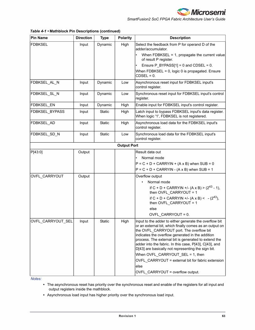
SmartFusion2 SoC FPGA Fabric Architecture User’s Guide
Revision 1 63
FDBKSEL Input Dynamic High Select the feedback from P for operand D of the adder/accumulator.
• When FDBKSEL = 1, propagate the current valueof result P register.
• Ensure P_BYPASS[1] = 0 and CDSEL = 0.
When FDBKSEL = 0, logic 0 is propagated. Ensure CDSEL = 0.
FDBKSEL_AL_N Input Dynamic Low Asynchronous reset input for FDBKSEL input's control register.
FDBKSEL_SL_N Input Dynamic Low Synchronous reset input for FDBKSEL input's control register.
FDBKSEL_EN Input Dynamic High Enable input for FDBKSEL input's control register.
FDBKSEL_BYPASS Input Static High Latch input to bypass FDBKSEL input's data register. When logic '1', FDBKSEL is not registered.
FDBKSEL_AD Input Static High Asynchronous load data for the FDBKSEL input's control register.
FDBKSEL_SD_N Input Static Low Synchronous load data for the FDBKSEL input's control register.
Output Port
P[43:0] Output Result data out
• Normal mode
P = C + D + CARRYIN + (A x B) when SUB = 0
P = C + D + CARRYIN - (A x B) when SUB = 1
OVFL_CARRYOUT Output Overflow output
• Normal mode
if C + D + CARRYIN +/- (A x B) > (243 - 1), then OVFL_CARRYOUT = 1
if C + D + CARRYIN +/- (A x B) < - (243), then OVFL_CARRYOUT = 1
else
OVFL_CARRYOUT = 0.
OVFL_CARRYOUT_SEL Input Static High Input to the adder to either generate the overflow bit or an external bit, which finally comes as an output on the OVFL_CARRYOUT port. The overflow bit indicates the overflow generated in the addition process. The external bit is generated to extend the adder into the fabric. In this case, P[43], C[43], and D[43] are basically not representing the sign bit.
When OVFL_CARRYOUT_SEL = 1, then
OVFL_CARRYOUT = external bit for fabric extension
else
OVFL_CARRYOUT = overflow output.
Table 4-1 • Mathblock Pin Descriptions (continued)
Pin Name Direction Type Polarity Description
Notes:
• The asynchronous reset has priority over the synchronous reset and enable of the registers for all input and output registers inside the mathblock.
• Asynchronous load input has higher priority over the synchronous load input.

Mathblocks
64 Revision 1
CDOUT[43:0] Output Cascade output of result P. CDOUT is same as P. It is used to drive the CDIN of another mathblock.
P_ARST_N[1:0] Input Dynamic Low Asynchronous reset input for P and OVFL_CARRYOUT control registers
• P_ARST_N [1] is for OVFL_CARRYOUT andP[43:18]
• P_ARST_N [0] is for P[17:0]
When not registered, connect P_ARST_N [1:0] to logic 1.
In normal mode, ensure P_ARST_N [1] = P_ARST_N [0].
P_SRST_N[1:0] Input Dynamic Low Synchronous reset input for P and OVFL_CARRYOUT control registers
• P_SRST_N [1] is for OVFL_CARRYOUT andP[43:18]
• P_SRST_N [0] is for P[17:0]
When not registered, connect P_SRST_N [1:0] to logic 1.
In normal mode, ensure P_SRST_N [1] = P_SRST_N [0].
P_EN[1:0] Input Dynamic High Enable input for P and OVFL_CARRYOUT control registers
• P_EN[1] is for OVFL_CARRYOUT and P[43:18]
• P_EN[0] is for P[17:0]
When not registered, connect P_EN[1:0] to logic 1.
In normal mode, ensure P_EN[1] = P_EN[0].
P_BYPASS[1:0] Input Static High Latch input for P and OVFL_CARRYOUT control registers
• P_BYPASS[1] is for OVFL_CARRYOUT andP[43:18]
• P_BYPASS[0] is for P[17:0]
When not registered, connect P_BYPASS[1:0] to logic 1.
In normal mode, ensure P_BYPASS[1] = P_BYPASS[0].
Table 4-2 • Truth Table for Propagating Operand D of the Adder/Accumulator
CDSEL FDBKSEL ARSHFT17 Operand D
0 0 0 0
0 0 1 0
1 X 0 CDIN[43:0]
1 X 1 17CDIN[43], CDIN[43:18]
Table 4-1 • Mathblock Pin Descriptions (continued)
Pin Name Direction Type Polarity Description
Notes:
• The asynchronous reset has priority over the synchronous reset and enable of the registers for all input and output registers inside the mathblock.
• Asynchronous load input has higher priority over the synchronous load input.

SmartFusion2 SoC FPGA Fabric Architecture User’s Guide
Revision 1 65
Mathblock ApplicationsThis section describes a few applications of SmartFusion2 SoC FPGA mathblocks.
35 x 35 MultiplierA 35 x 35 multiplier can be efficiently constructed using 4 mathblocks connected in cascade. This can be accomplished using 4 mathblocks in a single row. Multipliers are useful for applications which require more than 18-bit precision. Figure 4-4 shows a typical implementation of a non-pipelined 35 x 35 multiplier.
The inputs are assumed to be A[34:0] and B[34:0] and product as P[69:0].
0 1 0 P[43:0]
0 1 1 17P[43], P[43:18]
Table 4-2 • Truth Table for Propagating Operand D of the Adder/Accumulator
Figure 4-4 • Non-Pipelined 35 x 35 Multiplier
B [17:0]=0, B[34:17]H
A [17:0]=0, A[16:0]L
B [17:0]=0, B[34:17]H
A [17:0]=0, A[34:17]H
B [17:0]=0, B[16:0]L
A [17:0]=0, A[16:0]L
B [17:0]=0, B[16:0]L
A [17:0]=0, A[34:17]H
>>17
>>17
P[69:34]
P[16:0]
P[33:17]
0

Mathblocks
66 Revision 1
Pipelined Implementation of the 35 x 35 Multiplier SmartFusion2's SoC FPGA mathblocks have built-in registers on all input and output ports. If you want to implement a high-speed multiplier, extra pipeline registers can be inserted between the mathblocks using fabric registers. The non-pipelined 35 x 35 multiplication implementation shown in Figure 4-4 on page 65 will run at low clock speed. The non-pipelined implementation becomes even more inefficient for larger multiplications, because the critical path runs through the cascade of all mathblocks.
Figure 4-5 shows a typical 35 x 35 multiplier implementation with fabric pipeline registers.
In the above implementation, registers have been added to the output to allow high-speed operation. A few extra registers have been added to the input side or output side to balance the pipeline latency. These extra registers are implemented in the fabric logic modules.
Figure 4-5 • Pipeline 35 x 35 Multiplier
B [17:0]=0, B[34:17]H
A [17:0]=0, A[16:0]L
B [17:0]=0, B[34:17]H
A [17:0]=0, A[34:17]H
B [17:0]=0, B[16:0]L
A [17:0]=0, A[16:0]L
B [17:0]=0, B[16:0]L
A [17:0]=0, A[34:17]H
>>17
>>17
P[69:34]
P[16:0]
P[33:17]
0

SmartFusion2 SoC FPGA Fabric Architecture User’s Guide
Revision 1 67
Implementation of 9-Bit Complex Multiplication Considering two complex numbers X+jY, P+jQ, the complex multiplication is shown in EQ 1:
Multiplication Result = Real part + Imaginary Part = (PX - QY) + j (PY + QX)
EQ 1
Figure 4-6 shows the implementation of 9 x 9 complex multiplication using a mathblock configured in Dot-Product mode.
Complex multiplication implemented using a mathblock in dot-product mode requires additional 2's complement logic in the fabric for negating the Q input. The DOTP implementation in Figure 4-6 shows the optimized way of implementing the 2's complement with minimal logic in the fabric.
Figure 4-6 • 9-bit Complex Multiplication Using Dot-Product Mode
3-input Adder
X
Y
P
Q
44 PY+ QX9
9
9
9
<< 9
Dot Product ModeA
HB
LB
HA
L
MathBlock1
3-input Adder
X
Y
P
Q
44PX- QY9
9
9
9
<< 9
Dot Product ModeA
HB
LB
HA
L
MathBlock2
1’s complementLogic
(Imaginary Part)
(Real Part)
C[43:0]= Zero’s 44
C[43:19] = Zero’s C[9:0] = Zero’s
44
C[18:10]= Y
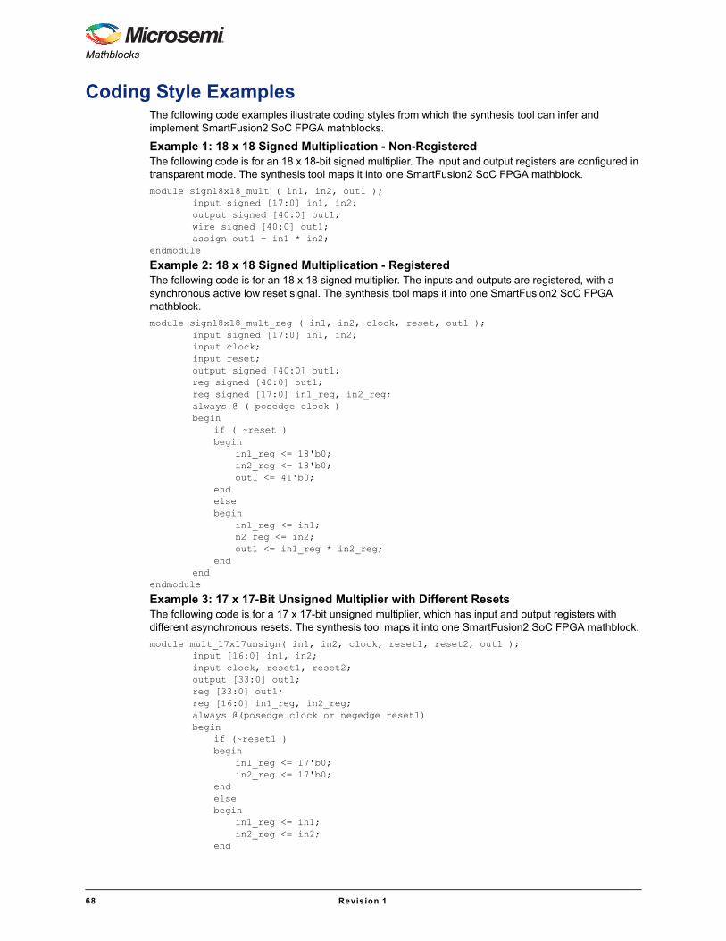
Mathblocks
68 Revision 1
Coding Style ExamplesThe following code examples illustrate coding styles from which the synthesis tool can infer and implement SmartFusion2 SoC FPGA mathblocks.
Example 1: 18 x 18 Signed Multiplication - Non-RegisteredThe following code is for an 18 x 18-bit signed multiplier. The input and output registers are configured in transparent mode. The synthesis tool maps it into one SmartFusion2 SoC FPGA mathblock.
module sign18x18_mult ( in1, in2, out1 );input signed [17:0] in1, in2;output signed [40:0] out1;wire signed [40:0] out1;assign out1 = in1 * in2;
endmodule
Example 2: 18 x 18 Signed Multiplication - RegisteredThe following code is for an 18 x 18 signed multiplier. The inputs and outputs are registered, with a synchronous active low reset signal. The synthesis tool maps it into one SmartFusion2 SoC FPGA mathblock.
module sign18x18_mult_reg ( in1, in2, clock, reset, out1 );input signed [17:0] in1, in2;input clock;input reset;output signed [40:0] out1;reg signed [40:0] out1;reg signed [17:0] in1_reg, in2_reg;always @ ( posedge clock )begin
if ( ~reset )begin
in1_reg <= 18'b0;in2_reg <= 18'b0;out1 <= 41'b0;
endelsebegin
in1_reg <= in1;n2_reg <= in2;out1 <= in1_reg * in2_reg;
endend
endmodule
Example 3: 17 x 17-Bit Unsigned Multiplier with Different ResetsThe following code is for a 17 x 17-bit unsigned multiplier, which has input and output registers with different asynchronous resets. The synthesis tool maps it into one SmartFusion2 SoC FPGA mathblock.
module mult_17x17unsign( in1, in2, clock, reset1, reset2, out1 );input [16:0] in1, in2;input clock, reset1, reset2;output [33:0] out1;reg [33:0] out1;reg [16:0] in1_reg, in2_reg;always @(posedge clock or negedge reset1)begin
if (~reset1 )begin
in1_reg <= 17'b0;in2_reg <= 17'b0;
endelsebegin
in1_reg <= in1;in2_reg <= in2;
end

SmartFusion2 SoC FPGA Fabric Architecture User’s Guide
Revision 1 69
endalways @(posedge clock or negedge reset2)begin
if (~reset2 )begin
out1 <= 34'b0;endelse
beginout1 <= in1_reg * in2_reg;
endend
endmodule
Example 4: 17 x 17-Bit Unsigned Multiplier with Different ClocksThis example shows an unsigned multiplier with inputs and outputs that are registered with different clocks: clock1 and clock2. In this case, the synthesis tool only packs the output registers and the multiplier into the SmartFusion2 SoC FPGA mathblock. The input registers are implemented in FPGA logic outside the SmartFusion2 SoC FPGA mathblock.
module mult_17x17unsign ( in1, in2, clock1, clock2, outl );input [16:0] in1, in2; input clock1,clock2; output [33:0] outl; reg [33:0] outl; reg [16:0] in1_reg, in2_reg;always @ ( posedge clock1 )begin
in1_reg <= in1;in2_reg <= in2;
end always @ ( posedge clock2 ) begin
outl <= in1_reg * in2_reg; end
endmodule
Example 5: Multiplier-Adder The code below shows a multiplier whose output is added with another input. The inputs and outputs are registered, and have enables and synchronous resets. The synthesis tool maps it into one SmartFusion2 SoC FPGA mathblock.
module mult_add_v1( in1, in2, in3, clock, reset, en, out1);input [16:0] in1, in2;input [33:0] in3;input clock, reset, en;output [34:0] out1;reg [34:0] out1;reg [16:0] in1_reg, in2_reg;reg [33:0] in3_reg;wire [33:0] mult_out;always @(posedge clock)beginif (~reset)begin
in1_reg <= 17'b0;in2_reg <= 17'b0;in3_reg <= 34'b0;
endelsebegin
if (en == 1'b1)beginin1_reg <= in1;in2_reg <= in2;in3_reg <= in3;

Mathblocks
70 Revision 1
endendendalways @(posedge clock)beginif (~reset)begin
out1 <= 35'b0;endelsebegin
if (en == 1'b1)begin
out1 <= 1'b0, mult_out + 1'b0, in3_reg;end
endendassign mult_out = in1_reg * in2_reg;
endmodule
Example 6: Multiplier-SubtractorThere are two ways to implement multiplier and subtract logic. The synthesis tool packs the logic differently, depending on which way it is implemented.
• Subtract the result of multiplier from an input value (P = Cin – mult_out). The synthesis tool packs all logic into the SmartFusion2 SoC FPGA mathblock.
• Subtract a value from the result of the multiplier (P = mult_out – Cin). The synthesis tool packs only the multiplier in the SmartFusion2 SoC FPGA mathblock. The subtractor is implemented in FPGA logic outside the mathblock.
– Unsigned MultSub Example (P = Cin – Mult_out) – Implemented in single mathblock.
module mult_sub ( in1, in2, in3, clk, rst, out1 );input [16:0] in1, in2;input [36:0] in3;input clk;input rst;output [39:0] out1;reg [39:0] out1;reg [16:0] in1_reg, in2_reg;always @ ( posedge clk )beginif (~rst)begin
in1_reg <= 17'b0;in2_reg <= 17'b0;out1 <= 40'b0;
endelsebegin
in1_reg <= in1;in2_reg <= in2;out1 <= in3 - (in1_reg * in2_reg);
endend
endmodule
– Unsigned MultSub Example (P = Mult – Cin) – Multiplier is implemented in mathblock and subtractor in FPGA logic
module mult_sub_v2 ( in1, in2, in3, clk, rst, out1 );input [16:0] in1, in2;input [36:0] in3;input clk;input rst;output [39:0] out1;reg [39:0] out1;
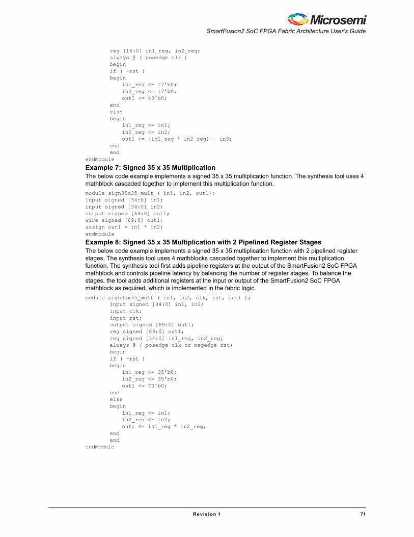
SmartFusion2 SoC FPGA Fabric Architecture User’s Guide
Revision 1 71
reg [16:0] in1_reg, in2_reg;always @ ( posedge clk )beginif ( ~rst )begin
in1_reg <= 17'b0;in2_reg <= 17'b0;out1 <= 40'b0;
endelsebegin
in1_reg <= in1;in2_reg <= in2;out1 <= (in1_reg * in2_reg) - in3;
endend
endmodule
Example 7: Signed 35 x 35 MultiplicationThe below code example implements a signed 35 x 35 multiplication function. The synthesis tool uses 4 mathblock cascaded together to implement this multiplication function.
module sign35x35_mult ( in1, in2, out1); input signed [34:0] in1; input signed [34:0] in2; output signed [69:0] out1; wire signed [69:0] out1; assign out1 = in1 * in2; endmodule
Example 8: Signed 35 x 35 Multiplication with 2 Pipelined Register StagesThe below code example implements a signed 35 x 35 multiplication function with 2 pipelined register stages. The synthesis tool uses 4 mathblocks cascaded together to implement this multiplication function. The synthesis tool first adds pipeline registers at the output of the SmartFusion2 SoC FPGA mathblock and controls pipeline latency by balancing the number of register stages. To balance the stages, the tool adds additional registers at the input or output of the SmartFusion2 SoC FPGA mathblock as required, which is implemented in the fabric logic.
module sign35x35_mult ( in1, in2, clk, rst, out1 ); input signed [34:0] in1, in2; input clk; input rst; output signed [69:0] out1; reg signed [69:0] out1; reg signed [34:0] in1_reg, in2_reg; always @ ( posedge clk or negedge rst) begin if ( ~rst ) begin
in1_reg <= 35'b0; in2_reg <= 35'b0; out1 <= 70'b0;
end else begin
ini_reg <= in1; in2_reg <= in2; out1 <= ini_reg * in2_reg;
end end
endmodule

Mathblocks
72 Revision 1
Glossary
Multi-ChannelingWhen multi-threading is done for a chain of mathblocks, its called multi-channeling.
Multi-ThreadingThe same mathblock can be used for performing more than one computation by time-multiplexing it.
Pipelined OperationThe mode of operation where the mathblock output is registered at the pipeline registers.
List of ChangesThe following table lists critical changes that were made in this chapter.
Date Changes Page
50200329-1/10.12 Modified Table 4-1. 59

Revision 1 73
5 – Fabric Global Routing Resources
This chapter describes the global routing architecture available in the SmartFusion®2 system-on-chip (SoC) field programmable gate array (FPGA) fabric devices and briefly discusses clocking resources, such as clock conditioning circuit (CCC) blocks, user phase-locked loops (PLLs), dedicated global I/Os, and virtual clock conditioning circuits (VCCCs).
Global Routing NetworkSmartFusion2 SoC FPGA devices offer a powerful, low skew global routing network which provides an effective clock distribution throughout the FPGA fabric. The global routing network of the SmartFusion2 SoC FPGA device has extensive support for multiple clock domains. In addition to handling distribution of clock signals, it can also be used for routing other global signals such as resets and presets.
The global routing network in the SmartFusion2 SoC FPGA device is a tightly coupled, hardwired, and dedicated routing network between the following types of buffers and clocking resources:
• CCCs with associated PLLs
• VCCCs
• Dedicated global I/Os
• Global blocks (GBs)
• Row global blocks (RGBs)
• Row global signals (RGs)
The global routing network provides a very low skew clock distribution network which spans the entire fabric area.
Figure 5-1 on page 74 shows the position of various global routing resources for an architecture which has two vertical stripes. This architecture is being used in the M2S050T device.

Fabric Global Routing Resources
74 Revision 1
The global routing network is divided into GBs and RGBs to allow segmenting. There are either 8 or 16 GBs available in the SmartFusion2 SoC FPGA devices, depending upon the global routing architecture available in the selected device. Each GB can generate one independent global signal. The global signals can be fed into the GBs from multiple sources such as, the dual-use global I/Os, CCC blocks, VCCC blocks, and fabric routing. There are hard-wired connections between GBs and CCCs, VCCCs and global I/Os. Figure 5-2 on page 75 and Figure 5-3 on page 76 show sources feeding into the GBs which finally feed into the RGBs to span the complete fabric area. An outside signal can come as input to the global I/Os, which then can route to the CCC blocks or VCCC blocks or directly to the GBs to be routed as the global signals.
Figure 5-1 • Position of Global Routing Resources in M2S050T
CCC – SW1
CCC – SW0
GBs
RGB
Row Global Signals
Clusters
Wes
t Sid
e G
loba
l I/O
s
South Side Global I/Os
Vertical Stripes
PLL
PLL
0 1 2 3 4 5 6 7 8 9 10 1112 131415
CCC – NW1PLL
CCC – NW0PLL
0123
4567
North Side Global I/Os0 1 2 3 4 5 6 7
CCC – NE1 PLL
CCC – NE0 PLL
0123
4567 E
ast Side Global I/O
s
VCCC – SE1
VCCC – SE0
0 1 2 3 4 5 6 7
Vertical Stripes

SmartFusion2 SoC FPGA Fabric Architecture User’s Guide
Revision 1 75
In a typical design scenario, the external clock can be fed to the dedicated global I/Os, which then can be routed to a CCC block or VCCC block. Each CCC block has a dedicated PLL associated with it. CCC blocks along with the associated PLL can perform various clock conditioning operations, such as clock multiplication, frequency division, phase shifting, delay cancellation, glitchless multiplexing of clocks sources, and delay insertion. The VCCC block is basically a 4x4 crossbar switch which is driven by dedicated global I/Os at its inputs and drives the GBs at its output. The VCCC enables any of the dedicated global I/Os at its input to reach any of the GBs driven by it. The clock signal, driven by the CCC or the VCCC block, is eventually routed to the GBs, which in turn drive the clock signal on to the global network. In another scenario, the clock from the dedicated global I/Os can go to the fabric for clock generation and then be routed to the GBs through the fabric routing. Furthermore, the external clock can be directly fed into the GBs from the dedicated global I/Os. The GBs can also be fed through regular I/Os, in which case the signals are first routed to fabric routing and then reach the GBs. Any signal generated from logic modules can reach the GBs through fabric routing.
The global signals routed through the GBs can drive all the logic modules across the fabric chip area through the RGBs on the fabric. The RGBs are situated on one or two vertical stripes inside the fabric in SmartFusion2 SoC FPGA devices. Smaller SmartFusion2 SoC FPGA device like M2S010T has 1 vertical stripe whereas large SmartFusion2 SoC FPGA device like M2S050T has 2 vertical stripes. Each RGB has right and left branches known as regional global rows. The clusters, each of which consists of 12 logic modules, are located on these branches. The global signals from the GBs get routed to independent RGBs which are then feed into the logic clusters located on the branches of the particular RGB. Any GB can drive any RGB on the fabric or any subset of the RGBs located in any of the vertical stripes of the chip, because the complete global network is segmented. Figure 5-1 on page 74 shows the top-level view of placements of the various global routing resources for the M2S050T SmartFusion2 SoC FPGA device.
All the global signals from CCCs or dedicated global I/Os must first reach the GBs and then they are distributed to the RGBs.
Each RGB, with its associated RGs, is independent and can be driven by fabric routing in addition to being driven by GBs. This enables you to use RGBs to drive regional clocks spanning a small fabric area.
Each CCC block can be accessed by 4 dedicated global I/Os and any one of them can provide the input clock source to the CCC. The CCC can also take inputs from fabric routing. Each CCC has access to either four or eight GBs, depending upon the global routing architecture present in the selected device. Similarly, each VCCC is driven by four dedicated global I/Os and each has access to either eight or four GBs. The fabric routing can drive eight GBs and the RGBs directly. Each RGB can drive the associated RG.
Figure 5-2 shows input sources to the GBs and RGBs for a larger device that has two vertical stripes.
Figure 5-3 on page 76 shows input sources to the GBs and RGBs for a smaller device that has one vertical stripe.
Figure 5-2 • Various Sources Feeding Global Blocks for a Bigger Device with 2 Vertical Stripes
Global Blocks(GB)
FabricInternal
Global I/Os
RGBRegional
Global Row - RGCCC
Fabric Routing
VCCC
4
4 16
8
8
8
Number of rows
PLL
8

Fabric Global Routing Resources
76 Revision 1
The complete global routing is done automatically by the place-and-route software: selection of GBs, CCCs, VCCCs, and finally the routing of global nets. You can select the placement of dedicated global I/Os according to your design requirement and the placement software will select the CCC/VCCCs and GBs as required.
All the global routing resources, including GBs and RGBs, have clock gating capability. Disabling the clocks to them results in power savings. The clock gating must be enabled by instantiating specific global clock buffers that have a clock, enable inputs, and a gated clock output. Figure 5-4 on page 77 shows the simplified circuit of the clock gating enabled clock buffer. You must connect the design’s main clock input, which can come from an I/O pad or can be generated internally, to the clock input of the clock gating buffer. You must then connect the clock gating enable input of the design to the enable input of the clock gating buffer. The gated clock output should then be fed into the various design regions. The place-and-route software maps the instantiated clock buffers to appropriate GBs or RGBs and enables the clock gating capability of the GBs or RGBs. The following is the list of clock gating enabled clock buffers:
• GCLKBUF (gated chip level clock buffer): Clock input is an external I/O; the macro has a routed EN pin to control the gate.
• GCLKBIBUF (gated chip level clock bidirectional buffer): Clock input is an external I/O; the macro has a routed EN pin to control the gate.
• GCLKINT (gated chip level internal clock buffer): Clock input is internally routed; the macro has a routed EN pin to control the gate.
• GRCLKINT (gated row level internal clock buffer): Clock input is internally routed; the macro has a routed EN pin to control the gate.
Figure 5-3 • Various Sources Feeding Global Blocks for a Smaller Device with One Vertical Stripe
Global Blocks(GB)
FabricInternal
Global I/Os
RGBRegional
Global Row - RGCCC
Fabric Routing
VCCC
4
4 8
8
4
4
Number of rows
PLL
8

SmartFusion2 SoC FPGA Fabric Architecture User’s Guide
Revision 1 77
The latch is transparent when the clock input is in low phase. The latch is in a hold state when the clock is in high phase. Figure 5-5 shows the timing waveforms for the clock gating enabled clock buffers.
If the EN signal changes during the clock high phase where the latch is in hold state, and if it satisfies the minimum hold time with respect to the prior rising clock edge, the latch output will only change after the falling clock edge, which subsequently enables or disables the clock high phase entirely.
If the EN signal changes during the clock low phase where the latch is transparent, the latch output will change immediately, and if it satisfies the minimum setup time with respect to the next rising clock edge, it will enable or disable the clock high phase entirely. If the enable signal EN violates either the setup or hold time with respect to the rising clock edge, the output behavior is unknown.
The CCCs also have the capability to gate its output and produce gated clock output, which can then be fed into the global clock routing network. Unused global resources such as RGBs and GBs are tied-off automatically to reduce dynamic power consumption.
The global routing network is not suitable for critical data signals because it has high latency and is inherently slow. In addition to high latency, it also has high insertion delay, which adds to the overall delay.
Routing critical data signals using the global network may result in timing violations and failure to meet timing requirements. The global network is best suited for clock signals and other global signals such as resets and presets.
Figure 5-4 • Clock Gating Enabled Clock Buffer Circuit
0
1EN
Clock
Gated Clock
Clock Gating Circuit
Latch
Figure 5-5 • Timing Waveforms for the Clock Gating Circuitry
Clock
EN
gated clock
latch output
setup time setup timehold time hold time

Fabric Global Routing Resources
78 Revision 1
Table 5-1 shows the number of resources available in the SmartFusion M2S050T device.
Clocking Resources
CCCThere are two, four, or six CCC blocks available in the SmartFusion2 SoC FPGA device, depending on the specific device.
The CCC block allows you to specify a flexible clocking scheme for designs implemented in the FPGA fabric of the SmartFusion2 SoC FPGA device. It can also be used to generate the base clock for the microcontroller subsystem (MSS).
Each CCC block operates dynamically with a dedicated user PLL and generates clock signals to the global network and FPGA core. You have the freedom to use any of the available user PLLs and CCCs to generate fabric clocks. You can use these CCCs and user PLLs by instantiating the CCC primitive in the design and configuring the CCC primitive as required for generating the various clocks for designs. The CCCs can receive inputs from dedicated global I/Os or the associated PLL, fabric routing, the two on-chip oscillators (1 MHz oscillator and 25 MHz – 50 MHz oscillator), or the external crystal oscillator.
The CCC block and associated PLLs provide the following clock conditioning capabilities to the SmartFusion2 SoC FPGA devices:
• Clock frequency multiplication
• Clock frequency division
• Phase shifting
• Clock-to-output or clock-to-input delay canceling
• Glitchless multiplexing between various clock input sources, including PLLs, FPGA fabric,oscillators, and global I/O pads.
• Programmable delay insertion on clocks
The clocks generated from CCCs can feed directly to the global network through the GBs.
For more details on the CCC block, refer to the SmartFusion2 On-Chip Oscillators, PLLs, and Clock Conditioning Circuitry User’s Guide.
Table 5-1 • Number of Resources in M2S050T Device
Resource Name
Number of Resources Available in
M2S050T Description
Global blocks 16 Located in the center of the fabric.
Vertical stripes 2 1 on either side of the fabric.
RGBs 1088 544 in each vertical stripe.
RGBs associated with each RG rows
8 These drive the right and left branches on each RG row.
CCC 6
2 on the southwest side of the fabric designated as CCC SW # 0 and CCC SW # 1.
2 on the northwest side of the fabric designated as CCC NW # 0 and CCC NW # 1.
2 on the northeast side of the fabric designated as CCC NE #0 and CCC NE #1.
VCCC 2 2 on the southeast side of the fabric designated as VCCC SE #0 and VCCC SE #1.
Dedicated Global I/Os 32 8 each on north, east, south, and west sides of the fabric.
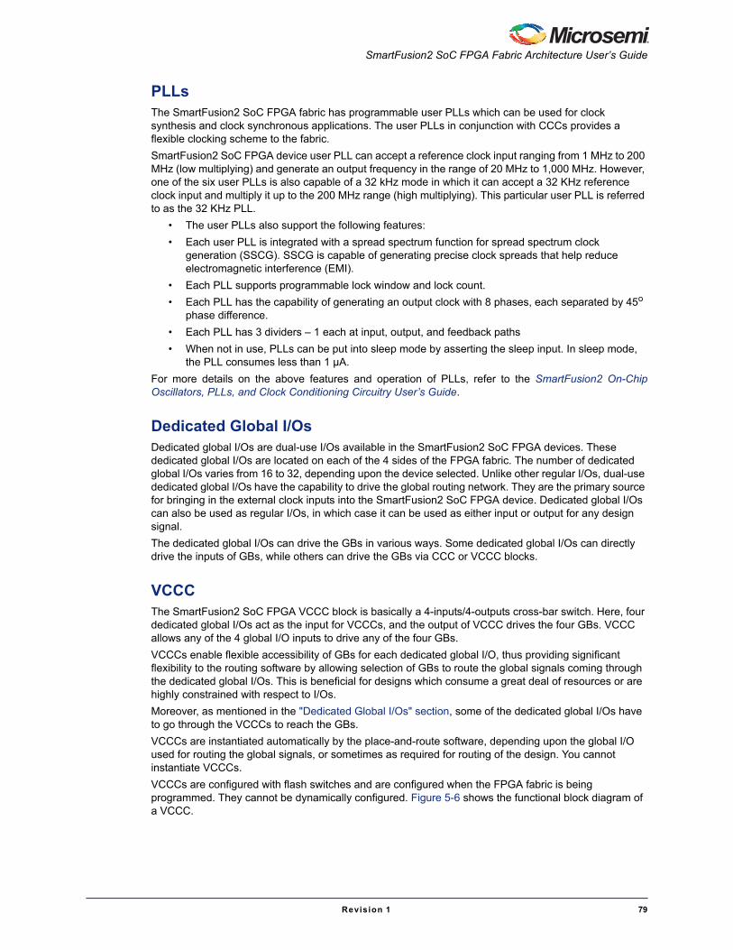
SmartFusion2 SoC FPGA Fabric Architecture User’s Guide
Revision 1 79
PLLsThe SmartFusion2 SoC FPGA fabric has programmable user PLLs which can be used for clock synthesis and clock synchronous applications. The user PLLs in conjunction with CCCs provides a flexible clocking scheme to the fabric.
SmartFusion2 SoC FPGA device user PLL can accept a reference clock input ranging from 1 MHz to 200 MHz (low multiplying) and generate an output frequency in the range of 20 MHz to 1,000 MHz. However, one of the six user PLLs is also capable of a 32 kHz mode in which it can accept a 32 KHz reference clock input and multiply it up to the 200 MHz range (high multiplying). This particular user PLL is referred to as the 32 KHz PLL.
• The user PLLs also support the following features:
• Each user PLL is integrated with a spread spectrum function for spread spectrum clock generation (SSCG). SSCG is capable of generating precise clock spreads that help reduce electromagnetic interference (EMI).
• Each PLL supports programmable lock window and lock count.
• Each PLL has the capability of generating an output clock with 8 phases, each separated by 45o phase difference.
• Each PLL has 3 dividers – 1 each at input, output, and feedback paths
• When not in use, PLLs can be put into sleep mode by asserting the sleep input. In sleep mode, the PLL consumes less than 1 µA.
For more details on the above features and operation of PLLs, refer to the SmartFusion2 On-ChipOscillators, PLLs, and Clock Conditioning Circuitry User’s Guide.
Dedicated Global I/OsDedicated global I/Os are dual-use I/Os available in the SmartFusion2 SoC FPGA devices. These dedicated global I/Os are located on each of the 4 sides of the FPGA fabric. The number of dedicated global I/Os varies from 16 to 32, depending upon the device selected. Unlike other regular I/Os, dual-use dedicated global I/Os have the capability to drive the global routing network. They are the primary source for bringing in the external clock inputs into the SmartFusion2 SoC FPGA device. Dedicated global I/Os can also be used as regular I/Os, in which case it can be used as either input or output for any design signal.
The dedicated global I/Os can drive the GBs in various ways. Some dedicated global I/Os can directly drive the inputs of GBs, while others can drive the GBs via CCC or VCCC blocks.
VCCCThe SmartFusion2 SoC FPGA VCCC block is basically a 4-inputs/4-outputs cross-bar switch. Here, four dedicated global I/Os act as the input for VCCCs, and the output of VCCC drives the four GBs. VCCC allows any of the 4 global I/O inputs to drive any of the four GBs.
VCCCs enable flexible accessibility of GBs for each dedicated global I/O, thus providing significant flexibility to the routing software by allowing selection of GBs to route the global signals coming through the dedicated global I/Os. This is beneficial for designs which consume a great deal of resources or are highly constrained with respect to I/Os.
Moreover, as mentioned in the "Dedicated Global I/Os" section, some of the dedicated global I/Os have to go through the VCCCs to reach the GBs.
VCCCs are instantiated automatically by the place-and-route software, depending upon the global I/O used for routing the global signals, or sometimes as required for routing of the design. You cannot instantiate VCCCs.
VCCCs are configured with flash switches and are configured when the FPGA fabric is being programmed. They cannot be dynamically configured. Figure 5-6 shows the functional block diagram of a VCCC.
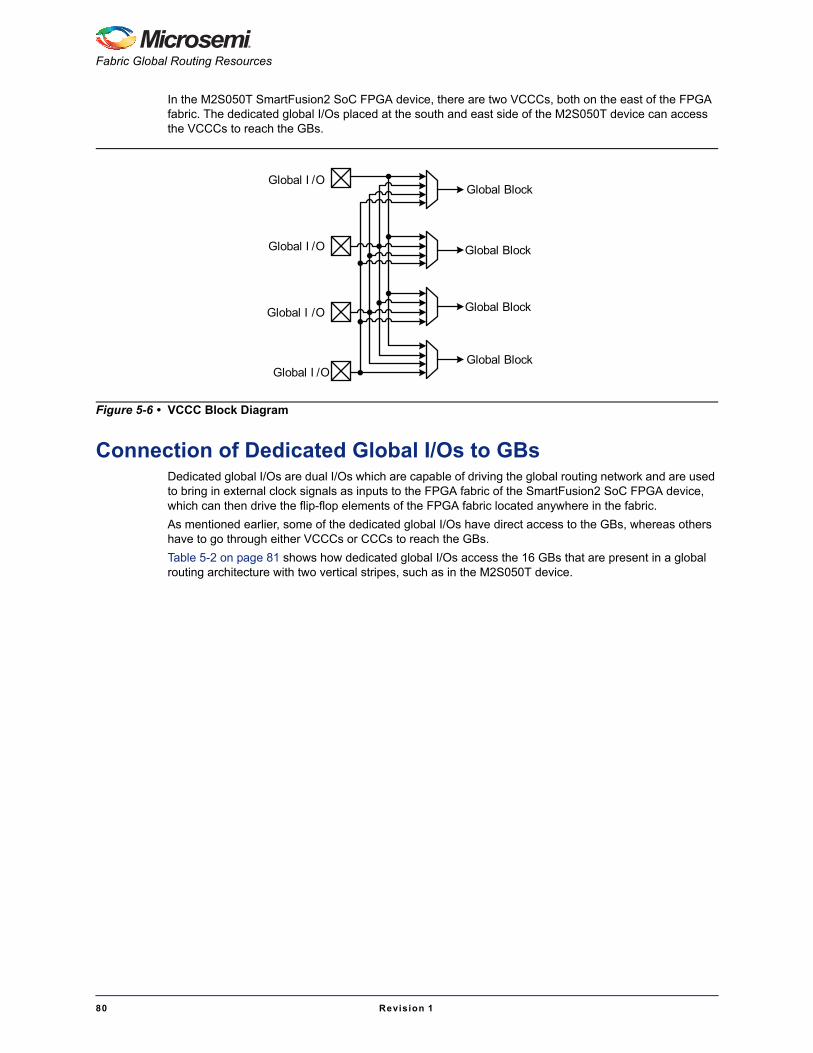
Fabric Global Routing Resources
80 Revision 1
In the M2S050T SmartFusion2 SoC FPGA device, there are two VCCCs, both on the east of the FPGA fabric. The dedicated global I/Os placed at the south and east side of the M2S050T device can access the VCCCs to reach the GBs.
Connection of Dedicated Global I/Os to GBsDedicated global I/Os are dual I/Os which are capable of driving the global routing network and are used to bring in external clock signals as inputs to the FPGA fabric of the SmartFusion2 SoC FPGA device, which can then drive the flip-flop elements of the FPGA fabric located anywhere in the fabric.
As mentioned earlier, some of the dedicated global I/Os have direct access to the GBs, whereas others have to go through either VCCCs or CCCs to reach the GBs.
Table 5-2 on page 81 shows how dedicated global I/Os access the 16 GBs that are present in a global routing architecture with two vertical stripes, such as in the M2S050T device.
Figure 5-6 • VCCC Block Diagram
Global Block
Global Block
Global Block
Global Block
Global I /O
Global I /O
Global I /O
Global I /O

Revision 1 81
SmartFusion2 SoC FPGA Fabric Architecture User’s Guide
Table 5-2 • GBs Accessed by Dedicated Global I/Os in Global Routing Architecture with Two Vertical Stripes
Global I/O Location
DedicatedGlobal I/Os
Connection to GBs Through
Southwest CCC Northwest CCC Northeast CCC Southeast VCCCDirect
Connection
0 1 0 1 0 1 0 1
West
Global I/O #0 GB#0, GB#4
Global I/O #1 GB#0, GB#4
Global I/O #2 GB#1, GB#5 GB#1
Global I/O #3 GB#1,GB#5 GB#5
Global I/O #4 GB#0, GB#4
Global I/O #5 GB#0,GB#4
Global I/O #6 GB#1, GB#5 GB#2
Global I/O #7 GB#1,GB#5 GB#6
North
Global I/O #0 GB#2, GB#6
Global I/O #1 GB#3, GB#7 GB#0
Global I/O #2 GB#2,GB#6 GB#4
Global I/O #3 GB#3,GB#7
Global I/O #4 GB#10, GB#14
Global I/O #5 GB#11,GB#15 GB#8
Global I/O #6 GB#10, GB#14 GB#12
Global I/O #7 GB#11, GB#15

Revision 1 82
SmartFusion2 SoC FPGA Fabric Architecture User’s Guide
East
Global I/O #0
Global I/O #1 GB#8, GB#12
Global I/O #2 GB#8, GB#12 GB#9
Global I/O #3 GB#8, GB#12 GB#13
Global I/O #4 GB#9, GB#13
Global I/O #5 GB#9, GB#13
Global I/O #6 GB#9, GB#13 GB#10
Global I/O #7 GB#9, GB#13 GB#14
South
Global I/O #0 GB#2, GB#6
Global I/O #1 GB#3, GB#7 GB#3
Global I/O #2 GB#2, GB#6 GB#7
Global I/O #3 GB#3, GB#7
Global I/O #4 GB#10, GB#14 GB#11
Global I/O #5 GB#11, GB#15 GB#10, GB#14 GB#15
Global I/O #6 GB#11, GB#15
Global I/O #7
Table 5-2 • GBs Accessed by Dedicated Global I/Os in Global Routing Architecture with Two Vertical Stripes (continued)
Global I/O Location
DedicatedGlobal I/Os
Connection to GBs Through
Southwest CCC Northwest CCC Northeast CCC Southeast VCCCDirect
Connection
0 1 0 1 0 1 0 1

SmartFusion2 SoC FPGA Fabric Architecture User’s Guide
Revision 1 83
If you are selecting a global I/O that has direct access to GBs, the routing software will directly route the global I/O input to the particular GB. If you have selected a global I/O in the east or south side which has access to the two VCCC blocks, the routing software will either route the global I/O directly or through VCCCs as per the routing requirements. If you have selected a global I/O as an input to a CCC block (CCC block instantiated in the design with input source selected as global I/O), the routing software will pick up an appropriate CCC block in the fabric, depending upon which global I/O is selected as input. In that case, the output of the CCC block will reach the GBs.
Glossary
Acronyms
CCC Clock conditioning circuit
EMIElectromagnetic interference
GBGlobal blocks
GCLKBIBUFGated chip-level clock bidirectional buffer
GCLKBUFGated chip-level clock buffer
GCLKINTGated chip-level internal clock buffer
GRCLKINTGated row level internal clock buffer
PLLPhase-locked loop
RGBRow global blocks
RGsRow global signals
SSCGSpread spectrum clock generation
VCCCVirtual clock conditioning circuits
Terminology
Global BlocksThe global buffers that can route global signal on to the global routing network.
Row Global BlocksThe global buffers are placed at the vertical stripes and are fed by the global signals from global blocks

Fabric Global Routing Resources
84 Revision 1
Row Global SignalsThese are the branches of the vertical stripes being fed by the row global blocks with the global signals.
Dual-Use Dedicated Global I/OsThese dual-use dedicated global I/Os have direct access to the global routing network via global blocks or VCCCs or CCCs. They can also act as normal I/Os.
ClustersClusters are formed by grouping a certain number of logic elements and interconnecting them. This is related to the clustered routing architecture of the SmartFusion2 SoC FPGA fabric.
Vertical StripesVertical stripes are the vertical columns on which the row global blocks are situated.
Glitchless MultiplexingThe CCC blocks has the capability of switching between different clock sources without producing any glitch on the output clocks.
List of ChangesThe following table lists critical changes that were made in this chapter.
Date Changes Page
50200329-1/10.12 Modified "Global Routing Network" section. 73

Revision 1 85
6 – I/Os
OverviewSmartFusion®2 system-on-chip (SoC) field programmable gate array (FPGA) devices have different types of input/outputs (I/Os), such as multi-standard I/Os (MSIO and MSIOD), double data rate I/Os (DDRIO), and dedicated I/Os based on the functional usage.
The MSIO, MSIOD and DDRIO provide programmable I/O features such as drive strength, slew rate, input delay, weak pull-up and weak pull-down for different voltage standards wherein users can configure and utilize them in different applications as needed. The programmable I/O features are explained in detail in the "I/O Programmable Features" on page 93.
The double data rate input output (DDRIO) is a multi-standard I/O optimized for LPDDR/DDR2/DDR3 performance. In the SmartFusion2 SoC FPGA devices there are two DDR subsystems: the Fabric DDR and MSS DDR controllers. DDRIOs can be connected to the respective DDR subsystem PHYs or can be used as user I/Os.
The MSIO, MSIOD, and DDRIO can be configured as MSS or fabric I/Os, whereas dedicated I/Os can be used for a single purpose such as SERDES, device reset, and clock functions. These dedicated I/Os cannot be used by any other circuits.
The MSIO, MSIOD and DDRIOs are configured at power-up by means of fabric-related flash bits, which are used to initialize registers blocks. The power-up sequence on the I/O is configured through the system controller and is responsible for controlling the power sequences.
I/O Functional DescriptionSmartFusion2 SoC FPGA devices feature a flexible I/O structure that supports a range of mixed voltages (1.2 V, 1.5 V, 1.8 V, 2.5 V, and 3.3 V) through bank selection. The MSIO, MSIOD and DDRIO can be configured as differential I/Os or two single-ended I/Os. These I/Os use two I/O slots to implement single-ended standards and differential standards.
Differential mode is implemented with a fixed I/O pair and cannot be split with adjacent I/Os. The differential standards are implemented as true differential outputs and not complementary single-ended outputs.
In single-ended mode, the I/O pair operates as two separate I/Os named P and N. All the configuration and data inputs/outputs are then separate and use names ending in P and N to differentiate between the two I/Os.
The fabric logic or MDDR/FDDR or MSS peripherals are connected to I/Os through IODs, as shown in Figure 6-1 on page 86. When MDDR/FDDR controller is used, Libero® System-on-Chip (SoC) automatically assigns the MDDR/FDDR controller signals to DDRIOs. In a similar way, when MSS peripheral is used, Libero SoC automatically assigns the MSS peripheral signals to MSIO/MSIODs. For fabric logic, you need to configure I/Os individually to function as input, output, and bidirectional.
The DDRIO is shared between fabric logic and MDDR/FDDR whereas MSIO/MSIOD is shared between MSS peripherals and fabric logic. The spio_sel signal, as shown in Figure 6-1 on page 86 decides the selection of MDDR/FDDR/MSS peripherals or fabric logic connecting to corresponding I/O.
When you do not use MDDR/FDDR controller or MSS peripherals, the respective I/Os are available to fabric logic. The selection (spio_sel) of FDDR/MDDR/MSS peripherals or fabric logic is made by a flash configuration bit and the logical state is configured during the programming.

I/Os
86 Revision 1
I/O consists of a highly featured bidirectional I/O buffer. The I/O is divided into two main sections:
• Digital – IOD (fabric and MDDR/FDDR/ MSS Peripherals)
• Analog – IOA
The digital (IOD) section generates output enable (OE), data out (DO), and data in (DIN) signals for both P and N IOA pairs.
The analog section (IOA) has transmitter and receiver buffers for the P and N pair. The main circuits in the IOA are transmitting and receiving buffers that support various I/O standards and contain the following modules:
• Transmit buffer
• Receive buffer
• Low power exit (LPE) logic
• On Die Termination
Figure 6-1 • I/O Interconnection with Fabric and MDDR/FDDR/ MSS Peripherals
Transmitter &Receiver
PAD
PAD
Differential
Differential
spio_sel
i/p buffer disable control
O/p buffer tristate control
IOA_P
IOA _N
Transmitter &Receiver
1
0
Data _out 1
Data _in1
DI_P
OE_P
DO_P
DI_P
Fabric IOD
Outreg01
Combinatorial
Outreg
Combinatorial
Inreg
Combinatorial
OE_P
DO_P
DI_P
IOD
Outreg
Combinatorial
Outreg
Combinatorial
Inreg
Combinatorial
User configures Fabric I/O in LiberoSoc
DO_P
Data _out 2
Data _in2Fabric Logic
DI_N
OE_N
DO_N
DI_N
Fabric IOD
Outreg01
Combinatorial
Outreg
Combinatorial
Inreg
Combinatorial
OE_N
DO_N
DI_N
IOD
OutregCombinatorial
OutregCombinatorial
Inreg
Combinatorial
User configures Fabric I/O in LiberoSoc
DO_N
01
1
0
spio_sel
en
User configures MDDR I/Os in Libero SoCLibero SoC configures MDDR/FDDR/MSSperipherals I/Os automatically 0
1
en
Fabric Logic
MSS Peripherals Or
MDDR / FDDR Controller + PHY
MSS Peripherals Or
MDDR / FDDR Controller + PHY
Libero SoC configures MDDR/FDDR/MSSperipherals I/Os automatically
User configures MDDR I/Os in Libero SoC
SmartFusion2 SoC FPGA Fabric Architecture User’s Guide
Revision 1 87
Transmit BufferTransmit and receive buffers transfer signals between the FPGA fabric and the IOA cells and also transfer signals between MSS DDR / fabric DDR / MSS peripherals and the IOA cells.
OE_P and OE_N control the direction of I/O buffers. When an I/O is operated as a single-ended I/O, OE_P and OE_N individually control the P and N I/O buffers. When an I/O is operated as a differential I/O, OE_P controls both the P and N I/O buffers.
The dynamic OE disables or enables an output buffer for all the standards.
Receive Buffer
You can enable or disable the input buffer, which is controlled by flash configuration bits and is configured during programming.
The I/O receiver can be made to operate in four different modes. These modes are selected based on flash configuration bits which are configured during programming after power-on. Following are the four modes of the receiver:
• True differential
• Pseudo-differential
• Single-ended
• Schmitt trigger
In true differential mode, P and N pad inputs are fed to the comparator, whereas in Pseudo-differential mode, each pad input is compared to reference with external reference voltage. Figure 6-2 on page 88 shows the detailed IOA structure of an I/O.
You can configure the I/O input as a Schmitt trigger receiver or single-ended receiver. When Schmitt trigger inputs are selected, the input buffers present hysteresis that filters the noise at the receiver and prevents double glitching caused by the noisy input edges.

I/Os
88 Revision 1
Low Power Exit Low power exit logic indicates to the system controller that designated I/Os have either matched the pre- defined signature bit or have detected activity on the selected I/O after the chip has entered Low-power mode.
For details on Signature and Activity modes, refer to the "Signature Mode" on page 100 and "Activity Mode" on page 100.
On-Die TerminationThe On-Die Termination (ODT) improves the signaling environment by reducing the electrical discontinuities introduced with off-die termination and hence enables reliable operation at higher signaling rates.
For more information on the programmed ODT values for DDRIO, MSIO and MSIOD, refer to the section "I/O Programmable Features" on page 93.
Figure 6-2 • IOA Architecture
DDRIOCalibration Block
Program directly ODT to desired value
Reference Resistor Value
44 -DDRIO Pairs Connected to MDDR / FDDR
-+
-+
Single- ended
Schmit
Psuedo - Differential
True- Differential
-+
Single- ended
Schmit
Psuedo- Differential
VCCIO
VCCIO
X_VREF
X_VREF
ODT /TransmitterImpedance
Input Programming Delay
OE_P
DO_P
DIN_P_delayed
Input Programming Delay
Fabricor
MDDR/FDDRor
MSS Peripherals
DIN_P
Differential
OE_N
DO_N
DIN_N_delayed
DIN_N
Programmable Slew rate for ‘P’ driver
Programmable Slew rate for ‘N’ driver Voltage Standard Select
Programmable Pull-up (or)Pull-down (or)
Disable both for ‘P’
Programmable Pull-up (or)Pull-down (or)
Disable both for ‘N’
PAD_P
PAD_N
IOA
Tx P
Receiver P
Tx N
Receiver N
10
10
ODT / TransmitterImpedance
DifferentialODT
(MSIOD only)
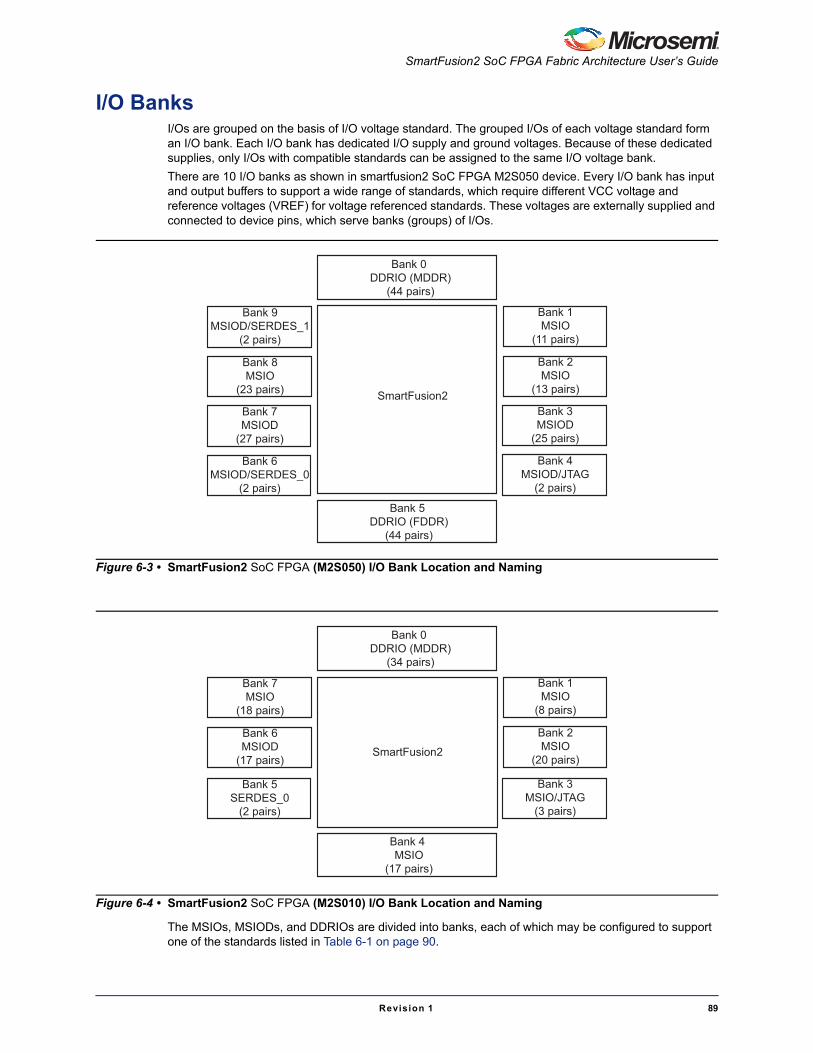
SmartFusion2 SoC FPGA Fabric Architecture User’s Guide
Revision 1 89
I/O BanksI/Os are grouped on the basis of I/O voltage standard. The grouped I/Os of each voltage standard form an I/O bank. Each I/O bank has dedicated I/O supply and ground voltages. Because of these dedicated supplies, only I/Os with compatible standards can be assigned to the same I/O voltage bank.
There are 10 I/O banks as shown in smartfusion2 SoC FPGA M2S050 device. Every I/O bank has input and output buffers to support a wide range of standards, which require different VCC voltage and reference voltages (VREF) for voltage referenced standards. These voltages are externally supplied and connected to device pins, which serve banks (groups) of I/Os.
The MSIOs, MSIODs, and DDRIOs are divided into banks, each of which may be configured to support one of the standards listed in Table 6-1 on page 90.
Figure 6-3 • SmartFusion2 SoC FPGA (M2S050) I/O Bank Location and Naming
Bank 0 DDRIO (MDDR)
(44 pairs)
Bank 5 DDRIO (FDDR)
(44 pairs)
SmartFusion2
Bank 9MSIOD/SERDES_1
(2 pairs)
Bank 6MSIOD/SERDES_0
(2 pairs)
Bank 7MSIOD
(27 pairs)
Bank 8MSIO
(23 pairs)
Bank 1MSIO
(11 pairs)
Bank 4MSIOD/JTAG
(2 pairs)
Bank 3MSIOD
(25 pairs)
Bank 2MSIO
(13 pairs)
Figure 6-4 • SmartFusion2 SoC FPGA (M2S010) I/O Bank Location and Naming
Bank 0 DDRIO (MDDR)
(34 pairs)
Bank 4 MSIO
(17 pairs)
SmartFusion2
Bank 7MSIO
(18 pairs)
Bank 5SERDES_0
(2 pairs)
Bank 6MSIOD
(17 pairs)
Bank 1MSIO
(8 pairs)
Bank 3MSIO/JTAG
(3 pairs)
Bank 2MSIO
(20 pairs)

I/Os
90 Revision 1
Table 6-1 shows the organization of I/O banks in SmartFusion2 SoC FPGA devices.
Supported I/O StandardsThe Table 6-2 shows supported voltage standards supported for various I/O types.
Table 6-1 • The Organization of I/O Banks in SmartFusion2 SoC FPGA Devices
I/O Banks M2S050* M2S010
Bank 0 DDRIO: MDDR or fabric DDRIO: MDDR or fabric
Bank 1 MSIO: MSS or fabric MSIO: MSS or fabric
Bank 2 MSIO: MSS or fabric MSIO: MSS or fabric
Bank 3 MSIO: MSS or fabric MSIO: JTAG/SWD
Bank 4 MSIO: JTAG/SWD MSIO: MSS or fabric
Bank5 DDRIO: FDDR or fabric MSIOD: SERDES_IF_0 or fabric
Bank 6 MSIOD: SERDES_IF_0 or fabric MSIOD: MSS or fabric
Bank 7 MSIOD: fabric MSIO: MSS or fabric
Bank 8 MSIO: fabric
Bank 9 MSIOD: SERDES_IF_0 or fabric
Note: *In the M2S050 device (Figure 6-2 on page 88), the DDRIOs are placed at the top and bottom of the device.There are 44 pairs (P, N) of DDRIOs located at both top and bottom side. DDRIOs placed at the topcommunicate with MDDR; those at the bottom communicate with FDDR. There are 31 MSIOD pairs and 23MSIO pairs placed on the left side of the device; 27 MSIOD pairs and 24 MSIO pairs on the right.
Table 6-2 • Supported Voltage Standards
I/O Standards
I/O Types
MSIO MSIOD DDRIO
Single-Ended I/O
LVTTL 3.3 V Yes – –
LVCMOS 3.3 V Yes – –
PCI Yes – –
LVCMOS 1.2 V Yes Yes Yes
LVCMOS 1.5 V Yes Yes Yes
LVCMOS 1.8 V Yes Yes Yes
LVCMOS 2.5 V Yes Yes Yes
Voltage-Referenced I/O
HSTL1.5V Yes Yes Yes
SSTL1.8 V Yes Yes Yes
SSTL2.5 V Yes Yes Yes
Differential I/O
SSTL 2.5 V(DDR1) Yes Yes Yes
SSTL 1.8V (DDR2) Yes Yes Yes
SSTL 1.5V (DDR3) Yes Yes Yes
LVPECL (input only) Yes – –
LVDS 3.3 V Yes – –
LVDS 2.5 V Yes Yes –
RSDS Yes Yes –
BLVDS Yes – –
MLVDS Yes – –
Mini-LVDS Yes Yes –

SmartFusion2 SoC FPGA Fabric Architecture User’s Guide
Revision 1 91
For I/O pin naming and assignments to specific banks, refer to the “Pin Descriptions” section in the SmartFusion2 customizable system-on-chip (cSoC) datasheet (to be released).
Single-Ended StandardsThese I/O standards use a push-pull CMOS output stage with a voltage referenced to system ground to designate logical states. The input buffer configuration, output drive, and I/O supply voltage (VCCI) vary among the I/O standards. The advantage of these standards is that a common ground can be used for multiple I/Os. This simplifies board layout and reduces system cost. Their reduced slew rate data transmission causes less electromagnetic interference (EMI) on the board. However, they are not suitable for high-frequency (>200 MHz) switching due to noise impact and higher power consumption.
Low Voltage TTL (LVTTL)This is a general purpose standard (EIA/JESD8-B) for 3.3 V applications. It uses an LVTTL input buffer and a push-pull output buffer. The LVTTL output buffer can have up to eight different programmable drive strengths.
Low Voltage CMOS (LVCMOS)SmartFusion2 SoC FPGA devices provide five different kinds of LVCMOS: LVCMOS 3.3 V, LVCMOS 2.5 V, LVCMOS 1.8 V, LVCMOS 1.5 V, and LVCOMS1.2 V. LVCMOS 3.3 V (only in MSIO) is an extension of the LVCMOS standard (JESD8-B compliant) used for general purpose 3.3 V applications. LVCMOS 2.5 V is an extension of the LVCMOS standard (JESD8-5-compliant) used for general purpose 2.5 V applications.
LVCMOS 1.8 V is an extension of the LVCMOS standard (JESD8-7-compliant) used for general purpose 1.8 V applications. The LVCMOS 1.5 V is an extension of the LVCMOS standard (JESD8-11-compliant) used for general purpose 1.5 V applications.
The VCCI values for these standards are 3.3 V, 2.5 V, 1.8 V, 1.5 V, and 1.2 V, respectively. All these versions use a 3.3 V-tolerant CMOS input buffer and a push-pull output buffer. Similar to LVTTL, the output buffer has up to eight different programmable drive strengths.
3.3 V Peripheral Component Interface (PCI)This standard specifies support for both 33 MHz and 66 MHz PCI bus applications. It uses an LVTTL input buffer and a push-pull output buffer. With the aid of an external resistor, this I/O standard can be 5 V-compliant.
Voltage-Referenced StandardsI/Os using these standards are referenced to an external reference voltage (VREF).
High-Speed Transceiver Logic (HSTL) Class I These are general purpose, high-speed 1.5 V bus standards (EIA/JESD8-6) for signaling between integrated circuits. The signaling range is 0 V to 1.5 V, and signals can be either single-ended or differential. HSTL requires a differential amplifier input buffer and a push-pull output buffer. These standards are used in the memory bus interface with data switching capability of up to 400 MHz. The other advantages of these standards are low power and fewer EMI concerns. HSTL has four classes, of which SmartFusion2 SoC FPGA devices support Class I. The reference voltage (VREF) is 0.75 V.
Stub Series Terminated Logic 2.5 V (SSTL2) Class I and II These are general purpose 2.5 V memory bus standards (JESD8-9) for driving transmission lines, designed specifically for driving the DDR SDRAM modules used in computer memory. The SSTL2 requires a differential amplifier input buffer and a push-pull output buffer. The reference voltage (VREF) is 1.25 V.
Stub Series Terminated Logic 1.8 V (SSTL18) Class I and II These are general purpose 1.8 V memory bus standards (JESD8-15) for driving transmission lines, designed specifically for driving the DDR2 SDRAM modules used in computer memory. SSTL18 requires a differential amplifier input buffer and a push-pull output buffer. The VREF is 0.9 V.

I/Os
92 Revision 1
Differential StandardsThese standards require two I/Os per signal (called a signal pair). Logic values are determined by the potential difference between the lines, not with respect to ground. This is why differential drivers and receivers have much better noise immunity than single-ended standards. The differential interface standards offer higher performance and lower power consumption than their single-ended counterparts. Two I/O pins are used for each data transfer channel. Differential standards require resistor termination on both I/Os.
Low Voltage Positive Emitter Coupled Logic (LVPECL) LVPECL requires that one data bit is carried through two signal lines; therefore, two pins are needed per input or output. It also requires external resistor termination. The voltage swing between the two signal lines is approximately 850 mV. When the power supply is +3.3 V, it is commonly referred to as LVPECL.
Low Voltage Differential Signal (LVDS) LVDS is a differential I/O standard. As with all differential signaling standards, LVDS requires that one data bit is carried through two signal lines, and it has inherent noise immunity over single-ended I/O standards. The voltage swing between two signal lines is approximately 350 mV. The external VREF or board termination voltage (VTT) is not required. LVDS requires the use of two pins per input or output.
Reduced Swing Differential Signaling (RSDS) A signaling standard that defines the output characteristics of a transmitter and inputs of a receiver along with the protocol for a chip-to-chip interface between flat-panel timing controllers and column drivers.
B-LVDS/M-LVDSBus LVDS (B-LVDS) refers to bus interface circuits based on LVDS technology. Multipoint LVDS (M-LVDS) specifications extend the LVDS standard to high-performance multipoint bus applications. Multi-drop and multipoint bus configurations may contain any combination of drivers, receivers, and transceivers. The LVDS drivers provide the higher drive current required by B-LVDS and M-LVDS to accommodate the bus loading.
The driver requires series terminations for better signal quality and to control voltage swing. Termination is also required at both ends of the bus, since the driver can be located anywhere on the bus.
Mini-LVDSA serial, intra-flat panel solution that serves as an interface between the timing control function and an LCD source driver.
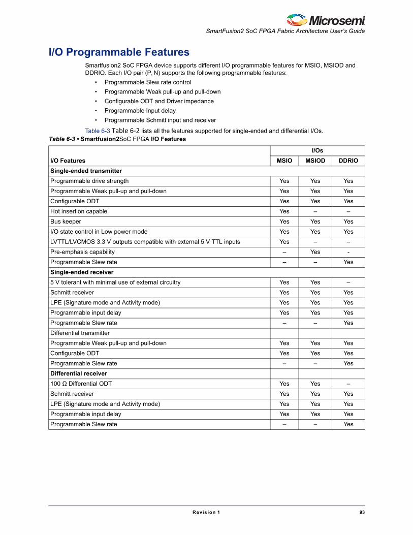
SmartFusion2 SoC FPGA Fabric Architecture User’s Guide
Revision 1 93
I/O Programmable FeaturesSmartfusion2 SoC FPGA device supports different I/O programmable features for MSIO, MSIOD and DDRIO. Each I/O pair (P, N) supports the following programmable features:
• Programmable Slew rate control
• Programmable Weak pull-up and pull-down
• Configurable ODT and Driver impedance
• Programmable Input delay
• Programmable Schmitt input and receiver
Table 6-3 Table 6‐2 lists all the features supported for single-ended and differential I/Os.Table 6-3 • Smartfusion2SoC FPGA I/O Features
I/O Features
I/Os
MSIO MSIOD DDRIO
Single-ended transmitter
Programmable drive strength Yes Yes Yes
Programmable Weak pull-up and pull-down Yes Yes Yes
Configurable ODT Yes Yes Yes
Hot insertion capable Yes – –
Bus keeper Yes Yes Yes
I/O state control in Low power mode Yes Yes Yes
LVTTL/LVCMOS 3.3 V outputs compatible with external 5 V TTL inputs Yes – –
Pre-emphasis capability – Yes -
Programmable Slew rate – – Yes
Single-ended receiver
5 V tolerant with minimal use of external circuitry Yes Yes –
Schmitt receiver Yes Yes Yes
LPE (Signature mode and Activity mode) Yes Yes Yes
Programmable input delay Yes Yes Yes
Programmable Slew rate – – Yes
Differential transmitter
Programmable Weak pull-up and pull-down Yes Yes Yes
Configurable ODT Yes Yes Yes
Programmable Slew rate – – Yes
Differential receiver
100 Ω Differential ODT Yes Yes –
Schmitt receiver Yes Yes Yes
LPE (Signature mode and Activity mode) Yes Yes Yes
Programmable input delay Yes Yes Yes
Programmable Slew rate – – Yes
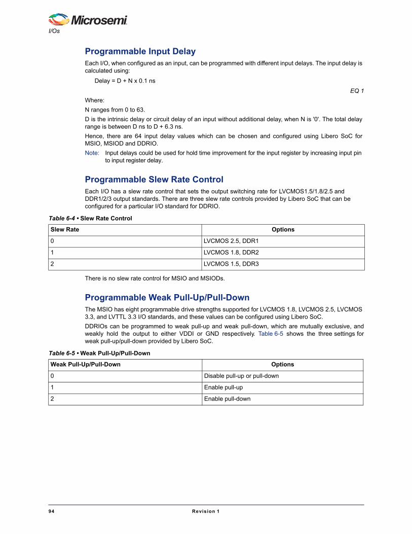
I/Os
94 Revision 1
Programmable Input Delay Each I/O, when configured as an input, can be programmed with different input delays. The input delay is calculated using:
Delay = D + N x 0.1 ns
EQ 1
Where:
N ranges from 0 to 63.
D is the intrinsic delay or circuit delay of an input without additional delay, when N is '0'. The total delay range is between D ns to D + 6.3 ns.
Hence, there are 64 input delay values which can be chosen and configured using Libero SoC for MSIO, MSIOD and DDRIO.
Note: Input delays could be used for hold time improvement for the input register by increasing input pin to input register delay.
Programmable Slew Rate ControlEach I/O has a slew rate control that sets the output switching rate for LVCMOS1.5/1.8/2.5 and DDR1/2/3 output standards. There are three slew rate controls provided by Libero SoC that can be configured for a particular I/O standard for DDRIO.
There is no slew rate control for MSIO and MSIODs.
Programmable Weak Pull-Up/Pull-DownThe MSIO has eight programmable drive strengths supported for LVCMOS 1.8, LVCMOS 2.5, LVCMOS 3.3, and LVTTL 3.3 I/O standards, and these values can be configured using Libero SoC.
DDRIOs can be programmed to weak pull-up and weak pull-down, which are mutually exclusive, andweakly hold the output to either VDDI or GND respectively. Table 6-5 shows the three settings forweak pull-up/pull-down provided by Libero SoC.
Table 6-4 • Slew Rate Control
Slew Rate Options
0 LVCMOS 2.5, DDR1
1 LVCMOS 1.8, DDR2
2 LVCMOS 1.5, DDR3
Table 6-5 • Weak Pull-Up/Pull-Down
Weak Pull-Up/Pull-Down Options
0 Disable pull-up or pull-down
1 Enable pull-up
2 Enable pull-down
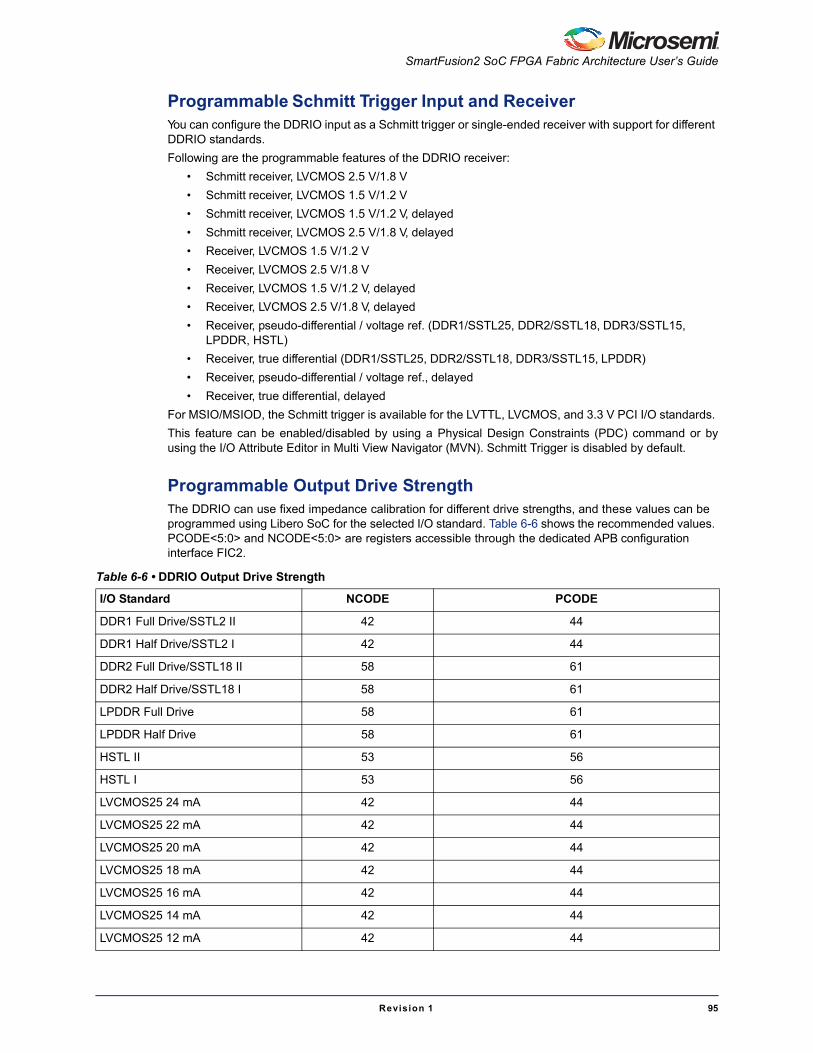
SmartFusion2 SoC FPGA Fabric Architecture User’s Guide
Revision 1 95
Programmable Schmitt Trigger Input and ReceiverYou can configure the DDRIO input as a Schmitt trigger or single-ended receiver with support for different DDRIO standards.
Following are the programmable features of the DDRIO receiver:
• Schmitt receiver, LVCMOS 2.5 V/1.8 V
• Schmitt receiver, LVCMOS 1.5 V/1.2 V
• Schmitt receiver, LVCMOS 1.5 V/1.2 V, delayed
• Schmitt receiver, LVCMOS 2.5 V/1.8 V, delayed
• Receiver, LVCMOS 1.5 V/1.2 V
• Receiver, LVCMOS 2.5 V/1.8 V
• Receiver, LVCMOS 1.5 V/1.2 V, delayed
• Receiver, LVCMOS 2.5 V/1.8 V, delayed
• Receiver, pseudo-differential / voltage ref. (DDR1/SSTL25, DDR2/SSTL18, DDR3/SSTL15, LPDDR, HSTL)
• Receiver, true differential (DDR1/SSTL25, DDR2/SSTL18, DDR3/SSTL15, LPDDR)
• Receiver, pseudo-differential / voltage ref., delayed
• Receiver, true differential, delayed
For MSIO/MSIOD, the Schmitt trigger is available for the LVTTL, LVCMOS, and 3.3 V PCI I/O standards.
This feature can be enabled/disabled by using a Physical Design Constraints (PDC) command or byusing the I/O Attribute Editor in Multi View Navigator (MVN). Schmitt Trigger is disabled by default.
Programmable Output Drive StrengthThe DDRIO can use fixed impedance calibration for different drive strengths, and these values can be programmed using Libero SoC for the selected I/O standard. Table 6-6 shows the recommended values. PCODE<5:0> and NCODE<5:0> are registers accessible through the dedicated APB configuration interface FIC2.
Table 6-6 • DDRIO Output Drive Strength
I/O Standard NCODE PCODE
DDR1 Full Drive/SSTL2 II 42 44
DDR1 Half Drive/SSTL2 I 42 44
DDR2 Full Drive/SSTL18 II 58 61
DDR2 Half Drive/SSTL18 I 58 61
LPDDR Full Drive 58 61
LPDDR Half Drive 58 61
HSTL II 53 56
HSTL I 53 56
LVCMOS25 24 mA 42 44
LVCMOS25 22 mA 42 44
LVCMOS25 20 mA 42 44
LVCMOS25 18 mA 42 44
LVCMOS25 16 mA 42 44
LVCMOS25 14 mA 42 44
LVCMOS25 12 mA 42 44

I/Os
96 Revision 1
LVCMOS25 10 mA 42 44
LVCMOS25 8 mA 42 44
LVCMOS25 6 mA 42 44
LVCMOS25 4 mA 42 44
LVCMOS25 2 mA 42 44
LVCMOS18 24 mA 58 61
LVCMOS18 22 mA 58 61
LVCMOS18 20 mA 58 61
LVCMOS18 18 mA 58 61
LVCMOS18 16 mA 58 61
LVCMOS18 14 mA 58 61
LVCMOS18 12 mA 58 61
LVCMOS18 10 mA 58 61
LVCMOS18 8 mA 58 61
LVCMOS18 6 mA 58 61
LVCMOS18 4 mA 58 61
LVCMOS18 2 mA 58 61
LVCMOS15 16 mA 53 56
LVCMOS15 14 mA 53 56
LVCMOS15 12 mA 53 56
LVCMOS15 10 mA 53 56
LVCMOS15 8 mA 53 56
LVCMOS15 6 mA 53 56
LVCMOS15 4 mA 53 56
LVCMOS15 2 mA 53 56
LVCMOS12 8 mA 40 42
LVCMOS12 6 mA 40 42
LVCMOS12 4 mA 40 42
LVCMOS12 2 mA 40 42
Table 6-6 • DDRIO Output Drive Strength (continued)
I/O Standard NCODE PCODE

SmartFusion2 SoC FPGA Fabric Architecture User’s Guide
Revision 1 97
Configurable ODT and Driver ImpedanceDDRIO has an ODT or transmitter impedance feature which is calibrated depending on the I/O standard. If the impedance feature is enabled, impedance can be programmed to the desired value in three ways. Figure 6-2 on page 88 shows the impedance configuration in DDRIO.
• Calibrate the ODT/driver impedance with a calibration block
• Calibrate the ODT/driver impedance with fixed calibration codes
• Configure the ODT/driver impedance to the desired value directly
There are two DDRIO calibration blocks in each SmartFusion2 SoC FPGA M2S050 device. The MDDR and FDDR have a DDRIO calibration block. Each calibration block calibrates ODT/driver impedance for all 44 DDRIO pairs (P, N).
Calibrate the ODT/Driver Impedance with Calibration BlockThe I/O calibration block calibrates the I/O drivers to an external resistor. The impedance control is used to identify the digital values PCODE<5:0> and NCODE<5:0>. These values are fed to the pull-up/pull-down reference network to match the impedance with an external resistor. Once it matches the PCODE and NCODE registers, they are latched and sent to the drivers.
Calibrated impedance value can be configured statically by enabling odt_static, or dynamically by enabling odt_dyn. Odt_static selects the ODT value set in flash configuration bits programmed during power-on, whereas odt_dyn selects the ODT value provided at run time.
Table 6-7 shows the ODT calibrated impedances for the following I/O standards:
Table 6-7 • ODT Calibrated Impedance
Driver Mode Reference Resistor (Ohm) Transmitter/ODT Calibrated Impedance
ODT, DDR3/SSTL 1.5, 1.5 V
240 120
240 60
240 40
240 30
240 20
ODT, DDR2/SSTL 1.8, 1.8 V
150 150
150 75
150 50
ODT, HSTL 191 47.8

I/Os
98 Revision 1
To calibrate driver/transmitter impedance for an I/O and calibration codes, you can configure the I/O to the calibrated impedance depending on the flash configuration bits for different I/O standards. Recommended reference resistor values used for calibration and the calibrated impedance values are shown in Table 6-8.
Calibrate the ODT/Driver Impedance with Fixed Calibration CodesYou can configure fixed calibration codes through the PCODE<5:0> and NCODE<5:0> registers. Libero SoC recommends using the fixed calibration codes provided in Table 6-5 on page 94.
Table 6-8 • Driver/Transmitter Calibrated Impedance
Driver Mode Reference Resistor (Ohm) Transmitter/ODT Calibrated Impedance
Transmitter, DDR3 SSTL 1.5 240 34
240 40
Transmitter, DDR3 SSTL 1.8 150 20
150 42
Transmitter, DDR3 SSTL 2.5 150 20
150 42
Transmitter, LPDDR SSTL 1.8 150 20
150 42
Transmitter, HSTL 1.5 191 25.5
191 47.8
LVCMOS 1.2 and 1.5 300 75
300 66.7
300 50
LVCMOS 1.8 150 75
150 50
150 33
150 25
LVCMOS 2.5 150 75
150 50
150 33
150 25

SmartFusion2 SoC FPGA Fabric Architecture User’s Guide
Revision 1 99
Configure the ODT/Driver Impedance Statically to Desired Value DirectlyYou can calibrate the ODT/driver to a desired value by providing PCODE<5:0> and NCODE<5:0> values directly through the dedicated APB configuration interface FIC2. In this configuration, the values are overwritten with existing values.
For MSIO and MSIOD, the ODT values shown in Table 6-7 are configured based on I/O standard.
I/O External Termination If ODT is not used, I/O standards require termination for better signal integrity. Voltage referencedstandards generally have a serial (driver) and parallel (receiver) termination whereas differential only hasparallel termination (receiver).
Table 6-10 shows external termination schemes for the I/O standards supported for DDRIO, MSIOand MSIOD when the ODT/driver impedance calibration feature is not used.
Table 6-9 • ODT Values
Standards ODT (MSIO) ODT (MSIOD)
LVDS 3.3 V 100 Ω NA
LVDS 2.5 V 100 Ω 100 Ω
BLVDS 100 Ω 100 Ω
RLVDS 100 Ω 100 Ω
SSTL 2I and SSTL 2II 50 Ω - 75 Ω - 150 Ω 50 Ω - 75 Ω - 150 Ω
SSTL 18I and SSTL 18II 50 Ω - 75 Ω - 150 Ω 50 Ω - 75 Ω - 150 Ω
HSTL I 50 Ω - 75 Ω - 150 Ω 50 Ω - 75 Ω - 150 Ω
Differential SSTL 2I and SSTL 2II 100 Ω 100 Ω
Differential SSTL 18I and SSTL 18II 100 Ω 100 Ω
Table 6-10 • Termination Schemes
I/O Standard External Termination Scheme
SSTL 1.5 single-ended (Class I & II)
Single-ended SSTL I/O standard terminationSSTL 1.8 single-ended (Class I & II)
SSTL 2 single-ended (Class II)
HSTL 1.5 single-ended (Class II) Single-ended HSTL I/O standard termination
SSTL 2.5 differential (Class I & II)
Differential SSTL I/O standard terminationSSTL 1.8 differential (Class I & II)
SSTL 1.5 differential (Class I & II)
HSTL 1.5 differential (Class II) Differential HSTL I/O standard termination
LVCMOS 2.5
No external termination requiredLVCMOS 1.8
LVCMOS 1.5
LVCMOS 1.2
LVDS 100 Ω, parallel termination
MLVDS 100 Ω, parallel termination
BLVDS 100 Ω, parallel termination
RLVDS 100 Ω, parallel termination
Mini LVDS 100 Ω, parallel termination
LVPECL 100 Ω, parallel termination
Note: To obtain more information on electrical characteristics, refer to the SmartFusion2 DataSheet (to be released).

I/Os
100 Revision 1
Low Power Signature Mode and Activity ModeThere are two modes for exiting Low-power mode: Signature mode and Activity mode. Flash configuration bits are used to configure I/Os to be disabled in Low-power mode, Signature mode, and Activity mode. Each DDRIO has four options for configuring and controlling low power exit:
• I/O not designated for low power exit monitoring
• I/O designated for low power activity monitoring
• I/O designated for low power signature, look for 0
• I/O designated for low power signature, look for 1
Signature ModeOnce entering Low-power mode, every I/O designated for signature I/O becomes input only. All other I/Os are tristated, held by bus hold, or weakly pulled-up/pulled-down. You have to drive a pattern to the signature I/O set during configuration. It checks for either 0 or 1, depending on the option selected. If all the signature values that are configured match the values at the pins, then the device exits Low-power mode.
Activity ModeIn Activity mode, the value at the pin of the activity I/O is latched before going to Low-power mode. When you configure I/Os as low power activity monitoring, the device exits Low-power mode if any activity is detected.
Bus KeeperThe main function is to weakly hold the signal on an I/O pin at its last driven state, holding it at a valid level with minimal power dissipation. The bus keeper circuitry also pulls undriven pins away from the input threshold voltage where noise can cause unintended oscillation. This feature is enabled or disabled using the flash configuration bits.
5 V Input Tolerance and Output Driving Compatibility (only MSIO)
5 V Input ToleranceI/Os can support 5 V input tolerance when LVTTL 3.3 V, LVCMOS 3.3 V, and LVCMOS 2.5 V configurations are used. There are three recommended solutions for achieving 5 V receiver tolerance. All the solutions meet a common requirement of limiting the voltage at the input to 3.45 V or less. In fact, the I/O absolute maximum voltage rating is 3.45 V, and any voltage above 3.45 V may cause long-term gate oxide failures.
Solution 1 The board-level design must ensure that the reflected waveform at the pad does not exceed the limits provided in the recommended operating conditions in the datasheet. This is a requirement to ensure long-term reliability.
This scheme also works for a 3.3 V PCI configuration, but the internal diode should not be used for clamping, and the voltage must be limited by the two external resistors. Relying on the diode clamping would create an excessive pad DC voltage of 3.3 V + 0.7 V = 4 V.
This solution requires two board resistors. Here are some examples of possible resistor values based on a simplified simulation model with no line effects and 10 Ω transmitter output resistance, where
Rtx_out_high = [VCCI – VOH] / IOH and Rtx_out_low = VOL / IOL).
EQ 2

SmartFusion2 SoC FPGA Fabric Architecture User’s Guide
Revision 1 101
Example 1 (high speed, high current):
Rtx_out_high = Rtx_out_low = 10 Ω
R1 = 36 Ω (±5%), P(r1)min = 0.069 Ω
R2 = 82 Ω (±5%), P(r2)min = 0.158 Ω
Imax_tx = 5.5 V / (82 × 0.95 + 36 × 0.95 + 10) = 45.04 mA
tRISE = tFALL = 0.85 ns at C_pad_load = 10 pF (includes up to 25% safety margin)
tRISE = tFALL = 4 ns at C_pad_load = 50 pF (includes up to 25% safety margin)
Example 2 (low-medium speed, medium current):
Rtx_out_high = Rtx_out_low = 10 Ω
R1 = 220 Ω (±5%), P(r1)min = 0.018 Ω
R2 = 390 Ω (±5%), P(r2)min = 0.032 Ω
Imax_tx = 5.5 V / (220 × 0.95 + 390 × 0.95 + 10) = 9.17 mA
tRISE = tFALL = 4 ns at C_pad_load = 10 pF (includes up to 25% safety margin)
tRISE = tFALL = 20 ns at C_pad_load = 50 pF (includes up to 25% safety margin)
Other values of resistors are also allowed as long as the resistors are sized appropriately to limit the voltage at the receiving end to 2.5 V < Vin(rx) < 3.6 V when the transmitter sends a logic 1. This range of Vin_dc(rx) must be assured for any combination of transmitter supply (5 V ± 0.5 V), transmitter output resistance, and board resistor tolerances.
Figure 6-5 • 5V Input Tolerance Solution 1
5.5 V
3.3 V
Rext1
Rext2
Requires two board resistorsLVCMOS3.3 V I/Os

I/Os
102 Revision 1
Solution 2The board-level design must ensure that the reflected waveform at the pad does not exceed the voltage overshoot/undershoot limits provided in the datasheet. This is a requirement to ensure long-term reliability. This scheme also works for a 3.3 V PCI configuration, but the internal diode should not be used for clamping, and the voltage must be limited by the external resistors and Zener. Relying on the diode clamping would create an excessive pad DC voltage of 3 V + 0.7 V = 4 V.
Solution 3The board-level design must ensure that the reflected waveform at the pad does not exceed the voltage overshoot/undershoot limits provided in the datasheet. This is a requirement to ensure long-term reliability.
5 V Output Driving CompatibilitySmartFusion2 SoC FPGA I/Os must be set to 3.3 V LVTTL or 3.3 V LVCMOS mode to reliably drive 5 V TTL receivers. It is also critical that there is NO external I/O pull-up resistor to 5 V, since this resistor would pull the I/O pad voltage beyond the 3.6 V absolute maximum value and consequently cause damage to the I/O. When set to 3.3 V LVTTL or 3.3 V LVCMOS mode, the I/Os can directly drive signals into 5 V TTL receivers. In fact, VOL = 0.4 V and VOH = 2.4 V in both 3.3 V LVTTL and 3.3 V LVCMOS modes exceeds the VIL = 0.8 V and VIH = 2 V level requirements of 5 V TTL receivers. Therefore, level 1 and level 0 are recognized correctly by 5 V TTL receivers.
Figure 6-6 • 5V Input Tolerance Solution 2
5.5 V 3.3 V
Rex
Requires one board resistors,one Zener 3.3 V diode, LVCMOS3.3 V I/Os
Zener3.3 V
Figure 6-7 • 5V Input Tolerance Solution 3
5.5 V 2.5 V2.5 V
Rex
On-chipclampdiode

SmartFusion2 SoC FPGA Fabric Architecture User’s Guide
Revision 1 103
Other I/O FeaturesFlash*FreezeUser logic in the FPGA fabric may request that the device enter Flash*Freeze mode by means of a system service request via the USI interface. During Flash*Freeze mode, a number of resources on the SmartFusion2 SoC FPGA devices are put into a low power state using the various power management hooks available for each resource. At design entry time, you can select which functional blocks go into low power state during Flash*Freeze mode.
Intelligent Wake-Up SmartFusion2 SoC FPGA devices have two ways to implement wake-up from Flash*Freeze mode:
• Real-time counter (RTC) timeout
• I/O cell wake-up
In the RTC timeout method, the timeout value is set in the RTC before entering Flash*Freeze mode.
In the I/O cell wake-up method, any activity on a specified input or by matching a user defined pattern value (signature) on a number of inputs wake up the device
I/Os in Conjunction with Fabric, MDDR/FDDR, and MSS Peripherals
DDRIOs with MDDR/FDDRIf you select MDDR/FDDR, Libero SoC automatically connects MDDR/FDDR signals to the DDRIOs. Depending on the memory configuration, only the required DDRIOs are used by Libero SoC. The unused DDRIO are available to you to connect to the FPGA fabric.
DDRIOs with FabricIf you do not select MDDR/FDDR, DDRIOs are available to the FPGA fabric. You must manually configure DDRIOs in Libero SoC.
MSIO/MSIODs with MSS PeripheralsIf you select MSS peripherals, Libero SoC automatically connects MSS peripheral signals to either MSIOs or to the MSIODs. The unused MSIOs or MSIODs are available to you to connect to the FPGA fabric.
MSIO/MSIODs with FabricIf you do not select MSS peripherals, MSIO/MSIODs are available to the FPGA fabric. You must manually configure MSIO/MSIOD in Libero SoC.

I/Os
104 Revision 1
JTAG I/O The system controller implements the functionality of a JTAG slave, with IEEE 1532 support, which also implies IEEE 1149.1 compliance. JTAG communicates with the system controller using a Command register that conveys the JTAG instruction to be executed and a 128-bit data I/O buffer that transfers any associated data. The TAP controller uses 8-bit instructions consistent with previous Microsemi families.
The JTAG pins can be run at any voltage from 1.5 V to 3.3 V (nominal). Core voltage must also be powered for the JTAG state machine to operate, even if the device is in Bypass mode. VJTAG alone is insufficient. Both VJTAG and core voltage to the SmartFusion2 SoC FPGA part must be supplied to allow JTAG signals to transition the SmartFusion2 SoC FPGA device. Isolating the JTAG power supply in a separate I/O bank gives greater flexibility with supply selection and simplifies power supply and PCB design, if the JTAG interface is neither used nor planned to be used the VJTAG pin together with the TRSTB pin should be tied to GND.
Table 6-11 • JTAG Pin Description
Name Type Bus Size Description
JTAGSEL In 1 JTAG controller selection
Depending on the state of the JTAGSEL pin, an external JTAG controller either sees the FPGA fabric TAP/auxiliary TAP (High) or the Cortex-M3 processor JTAG debug interface (Low).
The JTAGSEL pin should be connected to an external pull-up resistor such that the default configuration selects the FPGA fabric TAP.
TCK In 1 Test clock
Serial input for JTAG boundary scan, ISP, and UJTAG. The TCK pin does not have an internal pull-up/-down resistor. If JTAG is not used, Microsemi recommends tying it off.
TCK to GND or VJTAG through a resistor placed close to the FPGA pin. This prevents.
JTAG operation in case TMS enters an undesired state.
Note that to operate at all VJTAG voltages, 500 Ω to 1 k Ω satisfy the requirements.
Refer to Table 6-12 on page 105 for more information.
TDI In 1 Test data
Serial input for JTAG boundary scan, ISP, and UJTAG usage. There is an internal weak pull-up resistor on the TDI pin.
TDO Out 1 Test data
Serial output for JTAG boundary scan, ISP, and UJTAG usage.
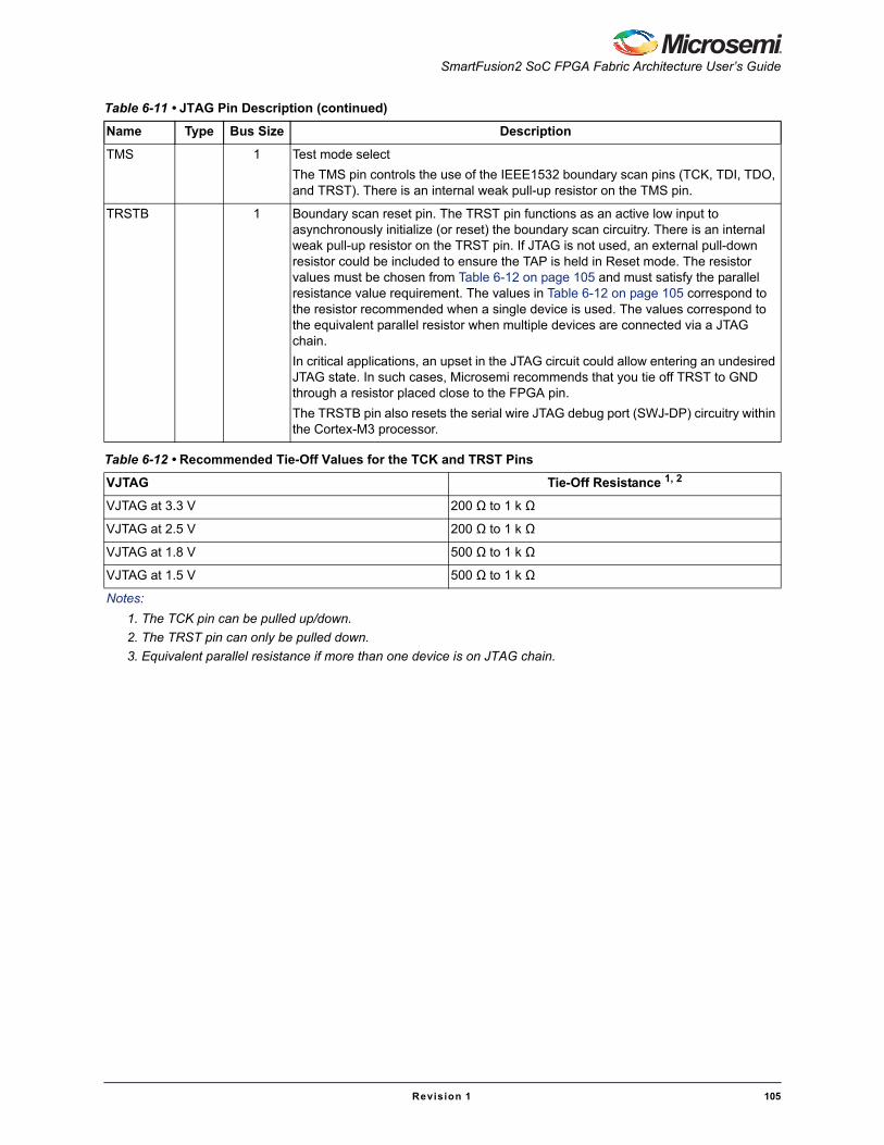
SmartFusion2 SoC FPGA Fabric Architecture User’s Guide
Revision 1 105
TMS 1 Test mode select
The TMS pin controls the use of the IEEE1532 boundary scan pins (TCK, TDI, TDO, and TRST). There is an internal weak pull-up resistor on the TMS pin.
TRSTB 1 Boundary scan reset pin. The TRST pin functions as an active low input to asynchronously initialize (or reset) the boundary scan circuitry. There is an internal weak pull-up resistor on the TRST pin. If JTAG is not used, an external pull-down resistor could be included to ensure the TAP is held in Reset mode. The resistor values must be chosen from Table 6-12 on page 105 and must satisfy the parallel resistance value requirement. The values in Table 6-12 on page 105 correspond to the resistor recommended when a single device is used. The values correspond to the equivalent parallel resistor when multiple devices are connected via a JTAG chain.
In critical applications, an upset in the JTAG circuit could allow entering an undesired JTAG state. In such cases, Microsemi recommends that you tie off TRST to GND through a resistor placed close to the FPGA pin.
The TRSTB pin also resets the serial wire JTAG debug port (SWJ-DP) circuitry within the Cortex-M3 processor.
Table 6-12 • Recommended Tie-Off Values for the TCK and TRST Pins
VJTAG Tie-Off Resistance 1, 2
VJTAG at 3.3 V 200 Ω to 1 k Ω
VJTAG at 2.5 V 200 Ω to 1 k Ω
VJTAG at 1.8 V 500 Ω to 1 k Ω
VJTAG at 1.5 V 500 Ω to 1 k Ω
Notes:
1. The TCK pin can be pulled up/down.
2. The TRST pin can only be pulled down.
3. Equivalent parallel resistance if more than one device is on JTAG chain.
Table 6-11 • JTAG Pin Description (continued)
Name Type Bus Size Description
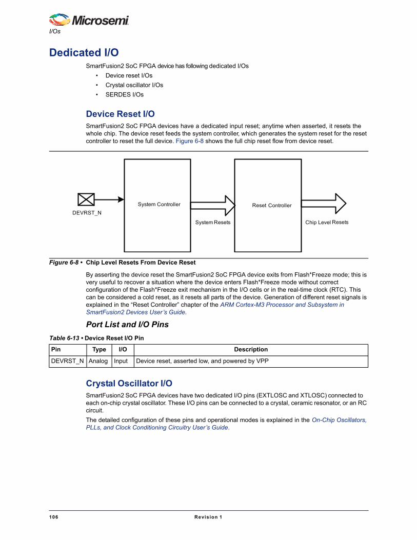
I/Os
106 Revision 1
Dedicated I/OSmartFusion2 SoC FPGA device has following dedicated I/Os
• Device reset I/Os
• Crystal oscillator I/Os
• SERDES I/Os
Device Reset I/OSmartFusion2 SoC FPGA devices have a dedicated input reset; anytime when asserted, it resets the whole chip. The device reset feeds the system controller, which generates the system reset for the reset controller to reset the full device. Figure 6-8 shows the full chip reset flow from device reset.
By asserting the device reset the SmartFusion2 SoC FPGA device exits from Flash*Freeze mode; this is very useful to recover a situation where the device enters Flash*Freeze mode without correct configuration of the Flash*Freeze exit mechanism in the I/O cells or in the real-time clock (RTC). This can be considered a cold reset, as it resets all parts of the device. Generation of different reset signals is explained in the “Reset Controller” chapter of the ARM Cortex-M3 Processor and Subsystem in SmartFusion2 Devices User’s Guide.
Port List and I/O Pins
Crystal Oscillator I/OSmartFusion2 SoC FPGA devices have two dedicated I/O pins (EXTLOSC and XTLOSC) connected to each on-chip crystal oscillator. These I/O pins can be connected to a crystal, ceramic resonator, or an RC circuit.
The detailed configuration of these pins and operational modes is explained in the On-Chip Oscillators, PLLs, and Clock Conditioning Circuitry User’s Guide.
Figure 6-8 • Chip Level Resets From Device Reset
System Controller Reset ControllerDEVRST_N
System Resets Chip Level Resets
Table 6-13 • Device Reset I/O Pin
Pin Type I/O Description
DEVRST_N Analog Input Device reset, asserted low, and powered by VPP
SmartFusion2 SoC FPGA Fabric Architecture User’s Guide
Revision 1 107
Crystal Oscillator I/O Pins
SERDES I/OThe SERDES I/Os available in SmartFusion2 SoC FPGA devices are dedicated to high speed serial communication protocols. The SERDES I/O supports protocols such as PCI Express 2.0, XAUI, serial gigabit media independent interface (SGMII), serial rapid I/O (SRIO), and any user-defined high speed serial protocol implementation in fabric. These protocols access the SERDES lanes through the physical media attachment (PMA) and physical coding sub layer (PCS) of the SERDES interface. The detailed configuration of the SERDES interface for various protocols is explained in the “SERDESIF Block” chapter of the High Speed Serial and DDR Interfaces User’s Guide. This section describes the SERDES I/O pins, SERDES I/O banks, SERDES I/O standards, and board-level design considerations available.
SERDES I/O PinsEach SERDES interface in the SmartFusion2 SoC FPGA device has four SERDES I/O data lanes or 16 SERDES I/Os available for accessing the SERDES interface (SERDESIF block). Each data lane has two pairs of differential signals: one for transmit data (TxDP, TxDN) and other for receive data (RxDP, RxDN). Data Ianes are multiplexed to support different serial protocols and scalable to various link widths—x1, x2, and x4. You can configure these settings in the SERDES_IF macro using Libero SoC design software. Each SERDES_IF has two sets of dedicated power, clock, and reference signals. One set for data lane 0 and 1 and another for data lane 2 and 3. Table 6-15 shows the SmartFusion2 SoC FPGA SERDES_IF I/O pins.
Table 6-14 • Crystal Oscillator I/O Pins
Pin Type I/O Description
EXTLOSC Analog Input Dedicated pin for a crystal external RC network connection.
XTLOSC Analog Input Dedicated pin to be used only for crystal connection.
Table 6-15 • SERDES I/O Pins Descriptions
Port Name TypeUnused
Condition Description
Data / Reference Pins
PCIE_x_RXDP0
PCIE_x_RXDP1
PCIE_x_RXDP2
PCIE_x_RXDP3
Input Unconnected Receive data. SERDES differential positive input: Each SERDES_IF consists of four RX+ signals. Here x=0 for SERDES_IF0 and x=1 for SERDES_IF1.
PCIE_x_RXDN0
PCIE_x_RXDN1
PCIE_x_RXDN2
PCIE_x_RXDN3
Input Unconnected Receive data. SERDES differential negative input: Each SERDES_IF consists of four RX- signals. Here x=0 for SERDES_IF0 and x=1 for SERDES_IF1.
PCIE_x_TXDP0
PCIE_x_TXDP1
PCIE_x_TXDP2
PCIE_x_TXDP3
Output Unconnected Transmit data. SERDES differential positive output: Each SERDES_IF consists of four TX+ signals. Here x=0 for SERDES_IF0 and x=1 for SERDES_IF1.
PCIE_x_TXDN0
PCIE_x_TXDN1
PCIE_x_TXDN2
PCIE_x_TXDN3
Output Unconnected Transmit data. SERDES differential negative output: Each SERDES_IF consists of four TX- signals. Here x=0 for SERDES_IF0 and x=1 for SERDES_IF1.

I/Os
108 Revision 1
SERDES I/O BanksThe SmartFusion2 SoC FPGA SERDES I/O resides on dedicated I/O banks. The number of SERDES I/Os depends on the device size and pin count. For example, the M2S050 device has two SERDES_IFs (SERDES_IF0, SERDES_IF1) which reside on two I/O banks (bank #6, bank #9) out of a total of ten I/O banks. The M2S010 device has one SERDES_IF (SERDES_IF0), which resides on one I/O bank #5.
Note: Refer to the SmartFusion2 Customizable System-on-Chip datasheet (to be released) for details onI/O bank location and I/O electrical specifications.
Common I/O Pins per SERDES Interface
PCIE_x_REXTL
PCIE_x_REXTR
Reference
Unconnected External reference resistor connection to calibrate TX/RX termination value. Each SERDES_IF consists of two REXT signals, one for lane 0 and 1 and another for lane 2 and 3. Here x=0 for SERDES_IF0 and x=1 for SERDES_IF1.
PCIE_x_VDDPLLL
PCIE_x_VDDPLLR
Power 2.5 V Analog power for the PLL of SERDES. Refer to the SmartFusion2 DataSheet (to be released) for exact voltage values.
Each SERDES_IF consists of two VDDPLL signals, one for lane 0 and 1 and another for lane 2 and 3. Here x=0 for SERDES_IF0 and x=1 for SERDES_IF1.
PCIE_x_PLLREFRETL
PCIE_x_PLLREFRETR
Power Unconnected PLL and reference resistor return path. Each SERDES_IF consists of two signals, one for lane 0 and 1 and other for lane 2 and 3. DO NOT short to GND on the package or PCB. For details, refer to the "Board Considerations for SERDES I/Os" on page 111. Here x=0 for SERDES_IF0 and x=1 for SERDES_IF1.
PCIE_x_VDDIOL
PCIE_x_VDDIOR
Power 1.2 V Tx/Rx analog I/O voltage. Refer to the SmartFusion2 DataSheet (to be released) for exact voltage values.
Each SERDES_IF consists of two VDDIO signals, one for lane 0 and 1 and another for lane2 and 3. Here x=0 for SERDES_IF0 and x=1 for SERDES_IF1.
PCIE_x_VSSIOL
PCIE_x_VSSIOR
Power Unconnected Tx/Rx VSS. Each SERDES_IF consists of two VSSIO signals, one for lane 0 and 1 and another for lane 2 and 3. Here x=0 for SERDES_IF0 and x=1 for SERDES_IF1.
PLL_PCIE_x_VDDA Power 3.3 V Auxiliary supply voltage by the core to the macro. Should be connected to VDDIO supply when standard does not require auxiliary power supply. Here x=0 for SERDES_IF0 and x=1 for SERDES_IF1.
PCIE_x_REFCLK0P
PCIE_x_REFCLK1P
Clock – Reference clock differential positive. Each SERDES_IF consists of two signals (REFCLK0_P, REFCLK1_P). These are dual purpose I/Os; when SERDES_IF is not used these lines can be used as MSIOD into FPGA fabric. Here x=0 for SERDES_IF0 and x = 1 for SERDES_IF1.
PCIE_x_REFCLK0N
PCIE_x_REFCLK1N
Clock – Reference clock differential negative. Each SERDES_IF consists of two signals (REFCLK0_P, REFCLK1_P). These are dual purpose I/Os; when SERDES_IF is not used these lines could be used as MSIOD into FPGA fabric. Here x=0 for SERDES_IF0 and x = 1 for SERDES_IF1.
Table 6-15 • SERDES I/O Pins Descriptions (continued)
Port Name TypeUnused
Condition Description

SmartFusion2 SoC FPGA Fabric Architecture User’s Guide
Revision 1 109
SERDES I/O SpecificationSERDES I/Os support high-speed differential I/O standard current mode logic (CML).
Figure 6-9, Figure 6-10, and Figure 6-11 on page 110 show example waveforms for the transmitter and receiver voltage levels.
VP: Single-ended peak voltage of TxDP
VN: Single-ended peak voltage of TxDN
VTX_DIFF_PP: Transmitter output differential peak-to-peak voltage
VTX_DE_EMPH_PP: Transmitter de-emphasize peak-to-peak voltage
VRX_DIFF_PP: Receiver input differential peak-to-peak voltage
VRX_EYE: Receiver eye voltage opening
TRX_EYE: Receiver eye time opening
Figure 6-9 • Single-Ended Voltage Levels (Example)
0 V
TxDP
TxDN
VP = 100 mV
VN = 500 mV 0 1 0
Figure 6-10 • Differential Voltage Levels (Example)
0 V
VDIFF = VTXDP – VTXDN VTX_DIFF_PP = 800 mV
VTX_DE_EMPH_PP

I/Os
110 Revision 1
AC CouplingEach lane of a link must be AC coupled. For AC coupling, capacitors are external to the chip and should be large enough to avoid excessive low frequency drop when the data signal contains a long string of consecutive identical bits. Suitable values (for example, 10 nF) for AC coupling capacitors (C1 and C2) must be used to maximize link signal quality and must conform to the SmartFusion2 DataSheet (to be released) electrical specifications. Each receiver differential signal terminates with a 50 Ohm resister to ground, as shown in Figure 6-12.
SERDES Pre-Cursor and Post-Cursor Emphasis and EqualizationWhen a high frequency signal propagates through a transmission line, high frequency components undergo attenuation compared to the low frequency components and finally the signal is severely distorted at the receiver. Pre-cursor and post-cursor emphasis and receiver equalization settings reduce the distortion of the signal due to effects of the transmission medium; configuration of these parameter values in the SERDES_IF macro are available in Libero SoC design software.
Note: Refer to the “SERDESIF Block” chapter of the High Speed Serial And DDR Interfaces User’sGuide for details on pre-cursor and post-cursor emphasis, receiver equalization settings, etc.
SERDES Return LossRefer to the SmartFusion2 datasheet for SERDES transmitter and receiver return loss parameters for differential and common modes.
Figure 6-11 • Receiver – Eye Diagram (Example)
VRX_EYE (min) = 100 mVPP(differential)
TRX_EYE
0 V
Figure 6-12 • AC Coupling and Differential Termination
TransmitterZo = 50 ohm
Receiver
Zo = 50 ohm
C1
C2
50 ohm 50 ohm

SmartFusion2 SoC FPGA Fabric Architecture User’s Guide
Revision 1 111
SERDES Reference Clock Requirements• The selection of the reference clock source or clock oscillator is characterized by frequency
range, output voltage swing, jitter (deterministic, random, peak-to-peak), rise and fall times, supply voltage and current, noise specification, duty cycle and duty cycle tolerance, and frequency stability.
• The reference clock must be within the range of 100 MHz to 160 MHz.
• The reference clock must be within the tolerance of the I/O standard specifications.
• The frequency of REFCLK can be modulated from +0% to –0.5% for the normal data rate frequency, at a modulation rate in the range supported by the protocols. The module supports both correlated and uncorrelated SSC.
• REFCLK jitter must be within the limits specified by the standards as seen at the input pin.
• In PCI Express, typically the input clock is a 100 MHz reference clock provided by the host slot for an endpoint device through the PCIe connector of the motherboard. If the two components connected through the PCIe bus use the same 100 MHz clock source, this is common Clock mode. In any other cases, the PCIe device is in separated Clock mode. The separated Clock mode thus corresponds to the case that one component does not use a 100 MHz reference clock, or a 100 MHz reference clock which does not have the same source and phase as the one used by the opposite component.
Note: Refer to the PCI Express Base Specification Rev2.1 for detailed PHY specifications.
Board Considerations for SERDES I/OsThis section explains the main board considerations for SERDES I/Os. The detailed board considerations for high speed interfaces are explained in the High Speed Board Design Manual for SmartFusion2 (to be released).
Microsemi recommends using low loss dielectric material for PCB construction for high speed and/or long trace (high attenuation) applications, especially with connectors in place.
• High speed traces should not be routed across a board area with many pin connectors.
• Vias on the PCB should be engineered for proper impedance as required by the application. Tune antipode spacing (capacitance) versus barrel inductance to achieve matched impedance.
• Avoid Via stubs by using back drill methods or without proper layout planning, especially for backplanes. Blind/buried vias can also be used as deemed appropriate, provided the via is engineered to appear as a matched output impedance in series with the trace. Otherwise, avoid vias that are predominantly capacitive at all cost.
• The reference planes on the board should be designed to have the lowest impedance possible, and should not be too tightly stacked.
• The board designer should give due consideration to the electrical performance issues such as dI/dt and IR drop.
• Crosstalk has to be minimized across all tracks and should be kept to fewer than 2% multi-active.
• Route differential pairs in the same layer as edge-coupled strip lines and avoid via jumps or any other impedance discontinuities. Avoid routing differential pairs as dual strip-lines. If the stackup of the board mandates routing as dual strip-lines, ensure that no tracks run parallel to the differential pairs and other sensitive signals to keep multi-active crosstalk under 2%.
• Minimize skew between the complimentary traces of the differential pair and equalize wire length and transmission line properties. If vias and other discontinuities are unavoidable, ensure that they are symmetrical.
• The mode of coupling (even/odd) of the differential pair should be based on the mode of coupling of the downstream connector.
• Group the TXDP/N traces and RXDP/N traces in different layers, if possible, for multi-lanes.
• Avoid tracks jumping in reference planes. If absolutely necessary, decouple the planes where jumps occur.

I/Os
112 Revision 1
• PLL Filter: To achieve a reasonable level of long term jitter, it is vital to deliver an analog grade power supply to the PLL. Typically an R-C or R-L-C filter is used, with the C being composed of multiple devices to achieve a wide spectrum of noise absorption. Although the circuit is simple, there are specific board layout requirements if it is to work at all.
– The series resistance of this filter is limited for DC reasons; generally it is recommended to see much less than 5% voltages drop across this device under worst-case conditions. Assuming that each SERDES VDDPLL current imposes a worst case of 1 mA, and assuming that VDDPLL is either 1.8 V or 2.5 V, depending on the chosen silicon process, then a drop of approximately 5% is expected across an 80–100 Ohm series resistor on VDDPLL for a single lane.
– The integration within the design of the single-lane SERDES_IF macros in Quad-configuration mode where 4 macros share one VDDPLL pin requires that in order to limit the drop to 5%, the series resistance must be no higher than 20–25 Ohms. The same calculation applies to dual-integrated macros, where 40 to 50 Ohm resistors apply.
– To achieve good low-frequency cut off, there should be a main ceramic or tantalum capacitor (~4.7 µF) in the filter design. As the filter needs to sustain its attenuation into moderately high frequencies, there is additionally at least one low equivalent series inductance (ESL) and low equivalent series resistance (ESR) capacitor in parallel (~100 nF ceramic capacitor in 0402 package). The routes from the high frequency capacitor(s) to the chip must be kept short and the capacitor must preferably be placed right underneath the chip on the reverse side of the board. Cursory analysis suggests that a third very high frequency capacitor should help reduce noise—but experimental data has not shown any jitter benefit in real applications.
– Board layout around the high-frequency capacitor and the path from there to the pads is critical. It is vital that the quiet ground and power are treated like analog signals.
– The package BGA ball pattern should ideally allow placement of 0402 or 0201 component assembly pads right across the VDDPLL and PLLREFRET pins behind the board. Solder reflow assembly of these components directly on the via barrel of the BGA pins without using appropriate landing pads result in low assembly yield and high cost. To avoid this, the BGA ball pattern must be arranged accordingly, with PCB assembly in mind.
– Given that the size of the parallel 4.7 µF capacitor may not allow its placement under the BGA pin field, the VDDPLL and PLLREFRET path must be the shortest possible power wires from the IC package pin to the low frequency capacitor, through the series resistor and finally to the board power. The distance from the IC pin to the high frequency capacitor should be as short as possible.
– The entire VDDPLL and PLLREFRET wiring path must not couple with any signal aggressors (especially any high swing and high slew rate signals such as TTL, CMOS, or SSTL signals used in DDR busses, etc.); trace shielding or line spacing management is required.
– PLLREFRET for this macro serves as the local on-chip ground return path for VDDPLL, so the external board ground must not short with PLLREFRET under any circumstances.
– High quality-factor series inductors should not be used without a series resistor when there is a high gain series resonator. In general, avoid using inductive chokes in any supply path unless care is taken to manage resonance.

SmartFusion2 SoC FPGA Fabric Architecture User’s Guide
Revision 1 113
– The power and ground traces should be short and should run parallel with adequate spacingto adjacent traces. VDDPLL or PLLREFRET are not to be connected directly to the boardpower planes. Refer to Figure 6-13 for proper connection.
• External Reference Resistor: It is required to use a high precision 1.2 K Ohm resistor in the 0402 or 0201 package for the external reference resistor connected between REXT and PLLREFRET.
– The power dissipation through this resistor is less than 1 mW during calibration. No power dissipates when the calibrator code is set to zeros.
– For every 1 pF of pin capacitance at REXT, it takes an extra 6.66 ns for voltages to settle. So the routes from the reference resistor to the chip must be kept as short as possible and the resistor must preferably be placed right underneath the chip on the reverse side of the board.
– Note that the capacitance of signal trace routes in FR4 is typically 4 pF/inch. Each additional inch of trace increases the RC settling time constant by about 5 ns and hence add an extra 20 ns for each step of the calibration process (assuming 4τ settling)
Placement of Critical Board Components: With the proper adjacent arrangement of package pins (VDDPLL, PLLREFRET and REXT, PLLREFRET) and choice of 1 mm pitch BGA for the package, the two critical components—approximately 100 nF high frequency decoupling capacitor and precision reference resistor—should be placed right underneath the chip on the reverse side of the board, as shown in Figure 6-12.
Figure 6-13 • Connections to Analog Power/Reference Pins
Figure 6-14 • Recommended Placement of Critical Components
2.5V20Ω
1.2KΩ
4.7μF 100nF
CHIPBOARD
PCIE_x_VDDPLLL
PCIE_x_PLLREFRETL
PCIE_x_REXTL
ChipBoard
Via
Component
I/Os
114 Revision 1
Glossary
Acronyms
DDRIODouble data rate input output
MDDRMicrocontroller subsystem double data rate
FDDRFabric double data rate
IOAInput output analog
IODInput output digital
LPDDRLow power double data rate memory
ODTOn-die termination
HSTLHigh-speed transceiver logic
SSTLStub series terminated logic
LVDSBus LVDS
Bus KeeperHolds the signal on an I/O pin at its last driven state.
ESDElectrostatic discharge protection
Hot InsertionCapability to connect I/O to external circuitry even after power-up.
HSTLHigh-speed transceiver logic
Low Power ExitLogic for the chip to come out from low power state.
LPELow power exit
LVDSLow-voltage differential signal
LVPECLLow-voltage positive emitter coupled logic

SmartFusion2 SoC FPGA Fabric Architecture User’s Guide
Revision 1 115
LVTTLLow voltage transistor transistor logic
MLVDSMultipoint LVDS
MSIOMulti-standard I/O
ODTOn die termination
RSDSReduced swing differential signaling
SSTLStub series terminated logic
SERDESSerializer/deserializer


Revision 1 117
7 – List of Changes
List of ChangesThe following table lists critical changes that were made in each revision.
Date Changes Page
50200329-1/10.12 Updated "Timing Diagrams" section (SAR 41640). 28
Updated "Read Operation" section (SAR 41640). 43
Updated "Mathblock Pin Descriptions" table (SAR 41834). 72
Updated "Global Routing Network" section (SAR 41770). 73
Note: *The part number is located on the last page of the document. The digits following the slash indicate the month and year of publication.


Revision 1 119
A – Product Support
Microsemi SoC Products Group backs its products with various support services, including CustomerService, Customer Technical Support Center, a website, electronic mail, and worldwide sales offices.This appendix contains information about contacting Microsemi SoC Products Group and using thesesupport services.
Customer ServiceContact Customer Service for non-technical product support, such as product pricing, product upgrades,update information, order status, and authorization.
From North America, call 800.262.1060From the rest of the world, call 650.318.4460Fax, from anywhere in the world, 408.643.6913
Customer Technical Support CenterMicrosemi SoC Products Group staffs its Customer Technical Support Center with highly skilledengineers who can help answer your hardware, software, and design questions about Microsemi SoCProducts. The Customer Technical Support Center spends a great deal of time creating applicationnotes, answers to common design cycle questions, documentation of known issues, and various FAQs.So, before you contact us, please visit our online resources. It is very likely we have already answeredyour questions.
Technical SupportVisit the Customer Support website (www.microsemi.com/soc/support/search/default.aspx) for more information and support. Many answers available on the searchable web resource include diagrams, illustrations, and links to other resources on the website.
WebsiteYou can browse a variety of technical and non-technical information on the SoC home page, at www.microsemi.com/soc.
Contacting the Customer Technical Support CenterHighly skilled engineers staff the Technical Support Center. The Technical Support Center can becontacted by email or through the Microsemi SoC Products Group website.
EmailYou can communicate your technical questions to our email address and receive answers back by email,fax, or phone. Also, if you have design problems, you can email your design files to receive assistance.We constantly monitor the email account throughout the day. When sending your request to us, pleasebe sure to include your full name, company name, and your contact information for efficient processing ofyour request.
The technical support email address is [email protected].

Product Support
120 Revision 1
My CasesMicrosemi SoC Products Group customers may submit and track technical cases online by going to My Cases.
Outside the U.S.Customers needing assistance outside the US time zones can either contact technical support via email([email protected]) or contact a local sales office. Sales office listings can be found atwww.microsemi.com/soc/company/contact/default.aspx.
ITAR Technical SupportFor technical support on RH and RT FPGAs that are regulated by International Traffic in Arms Regulations (ITAR), contact us via [email protected]. Alternatively, within My Cases, select Yes in the ITAR drop-down list. For a complete list of ITAR-regulated Microsemi FPGAs, visit the ITAR web page.


50200329-1/10.12
© 2012 Microsemi Corporation. All rights reserved. Microsemi and the Microsemi logo are trademarks ofMicrosemi Corporation. All other trademarks and service marks are the property of their respective owners.
Microsemi Corporation (NASDAQ: MSCC) offers a comprehensive portfolio of semiconductorsolutions for: aerospace, defense and security; enterprise and communications; and industrialand alternative energy markets. Products include high-performance, high-reliability analogand RF devices, mixed signal and RF integrated circuits, customizable SoCs, FPGAs, andcomplete subsystems. Microsemi is headquartered in Aliso Viejo, Calif. Learn more atwww.microsemi.com.
Microsemi Corporate HeadquartersOne Enterprise, Aliso Viejo CA 92656 USAWithin the USA: +1 (949) 380-6100Sales: +1 (949) 380-6136Fax: +1 (949) 215-4996