snvs839a – june 2012– revised march 2013 lm8330 · pdf fileplus 8 special function...
TRANSCRIPT

LM8330
www.ti.com SNVS839A –JUNE 2012–REVISED MARCH 2013
LM8330 I2C-Compatible Keypad Controller with GPIO, PWM, and IEC61000 ESD ProtectionCheck for Samples: LM8330
1FEATURES – Debounce Time for Reliable Key EventPolling
2• KEY FEATURES– Configuration of General Purpose I/O Ports– Keypad Matrices of up to of 8 x 12 Keys,– Various Initialization Options (Keypad Size,Plus 8 Special Function (SF) Keys, for a
etc.)Full 104 Key Support.• KEY DEVICE FEATURES– Supports General-purpose I/O Expansion
on Pins Not Otherwise Used for Keypad or – 1.8V ±10% Single-supply OperationPWM Output. – On-chip Power-on Reset (POR)
– Keypad Matrix and Dedicated Key Support: – −30°C to +85°C Temperature Range– 16-Event Keycode Buffer – Robust IEC ESD Protection: ±8 kV Direct– 4-Event Multiple Key Storage Registers Contact on KPX[7:0] and KPY[10:0] Pins
– Internal Oscillator, No External Clock – 25-pin DSBGA Package Size: 2 mm x 2 mmRequired. x 0.6 mm (0.4 mm Pitch)
– I2C-compatible ACCESS.bus Slave InterfaceAPPLICATIONS:Standard (100 kHz) and Fast (400 kHz)
Modes: • Mobile Phones– 7-bit and 10-bit Addressing • Qwerty Keyboard– Programmable Slave Address • Universal Remote– (Default 7-bit 0x88, 10-bit 0x088)
DESCRIPTION– Three Host-programmable PWM OutputsThe LM8330 I/O - Expander and Keypad Controller is– Smooth LED Brightness Modulationa dedicated device designed to unburden a host
– Dedicated 31-command Script Bugger processor from scanning a matrix-addressed keypad– Register-based Command Interpreter and to provide flexible and general purpose, host
programmable input/output functions. Threewith Auto-increment Addressingindependent Pulse Width Modulation (PWM) timer– Key Events, Errors, and Dedicatedoutputs are provided for dynamic LED brightnessHardware Interrupts, Request Host Servicemodulation.by Asserting an IRQ OutputIt communicates with a host processor through an– Ultra-Low-Power OperationI2C-compatible ACCESS.bus serial interface. It can
– Automatic HALT Mode: 1.5 µA (typ.) communicate in Standard (100 kHz) and Fast-Mode– Active Supply Current: 23 µA (typ.) (400 kHz) in slave Mode only.– Configurable Wake-Up from HALT All available input/output pins can alternately be used
Operation as an input or an output in a keypad matrix or as ahost-programmable general-purpose input or output.– IEC61000-4-2 ESD Protection on KPX[7:0]
and KPY[10:0] pins Any pin programmed as an input can also sense– ESD Glitch Filter on RESETN Input hardware interrupts. The interrupt polarity (“high-to-
low” or “low-to-high” transition) is thereby– External Reset for System Controlprogrammable.• HOST-CONTROLLED FEATURESThe LM8330 follows a predefined register-based set– Reset Input for System Controlof commands. Upon startup (power-on) a
– PWM Scripting for Three PWM Outputs configuration file must be sent from the host to set up– Period of Inactivity That Triggers Entry into the hardware of the device.
HALT Mode1
Please be aware that an important notice concerning availability, standard warranty, and use in critical applications ofTexas Instruments semiconductor products and disclaimers thereto appears at the end of this data sheet.
2All trademarks are the property of their respective owners.
PRODUCTION DATA information is current as of publication date. Copyright © 2012–2013, Texas Instruments IncorporatedProducts conform to specifications per the terms of the TexasInstruments standard warranty. Production processing does notnecessarily include testing of all parameters.

1 2 3 4 5
A
B
C
D
E
LM8330
Main processing
device
ACCESS.bus
CommandInterpreter
Input/OutputExpansion
SDA
SCL
RESETN
IRQN
1.8V (typ)
VCC
InternalOSC
DIV
32 kHz Reference
Clock
PWMGenerator
Key-ScanControl
Wake-UpControl
Keypad Matrix
PWM0
PWM1
PWM2
Input/OutputSleep Control
General PurposeInputs/Outputs
AS
IP E
SD
Pro
tect
ion
NOTE: This diagram illustrates IO configuration 3 with IRQN enabled
ASIP ESD Protection
0.1 PF (required)
LM8330
SNVS839A –JUNE 2012–REVISED MARCH 2013 www.ti.com
DESCRIPTION (CONTINUED)The LM8330 is available in a 25-bump lead-free DSBGA package size 2.0 mm x 2.0 mm x 0.6 mm (0.4 mmpitch).
The LM8330 has integrated ASIP (Application Specific Integrated Passives) on the KPX[7:0] and KPY[10:0] pins.These pins are designed to tolerate IEC61000-4-2 level 4 ESD: ±8 kV direct contact.
LM8330 FUNCTION BLOCKS
PACKAGE MARKING
Figure 1. LM8330 Pinout - Top View (balls underneath)
2 Submit Documentation Feedback Copyright © 2012–2013, Texas Instruments Incorporated
Product Folder Links: LM8330

LM8330
www.ti.com SNVS839A –JUNE 2012–REVISED MARCH 2013
SIGNAL DESCRIPTIONS
Primary and Alternate Functions of All Device PinsBall Function 0 (1) Function 1 (1) Function 2 (1) Function 3 (1) Pin Count Ball Name
A3 Reset Active Low Input 1 RESETN
D3 Supply Voltage 1 VCC
A4 ACCESS.bus Clock 1 SCL
A5 ACCESS.bus Data 1 SDA
E1 Keypad-I/O X0 GPIO0 1 KPX0
D2 Keypad-I/O X1 GPIO1 1 KPX1
B4 Keypad-I/O X2 GPIO2 1 KPX2
B5 Keypad-I/O X3 GPIO3 1 KPX3
A1 Keypad-I/O X4 GPIO4 1 KPX4
A2 Keypad-I/O X5 GPIO5 1 KPX5
C1 Keypad-I/O X6 GPIO6 1 KPX6
D1 Keypad-I/O X7 GPIO7 1 KPX7
E4 Keypad-I/O Y0 GPIO8 1 KPY0
E3 Keypad-I/O Y1 GPIO9 1 KPY1
E2 Keypad-I/O Y2 GPIO10 1 KPY2
D4 Keypad-I/O Y3 GPIO11 1 KPY3
B2 Keypad-I/O Y4 GPIO12 1 KPY4
B1 Keypad-I/O Y5 GPIO13 1 KPY5
C2 Keypad-I/O Y6 GPIO14 1 KPY6
B3 Keypad-I/O Y7 GPIO15 1 KPY7
C4 Keypad-I/O Y8 GPIO16 PWM2 (2) 1 KPY8
D5 Keypad-I/O Y9 GPIO17 PWM1 1 KPY9
E5 Keypad-I/O Y10 GPIO18 PWM0 1 KPY10
C5 Keypad-I/O Y11 GPIO19 PWM2 (2) Interrupt 1 IRQN
C3 Ground 1 GND
Total 25
(1) This table describes the alternate pin function and not the actual BALLCFG assignments. Refer to Table 49 for actual BALLCFGAssignments.
(2) PWM2 functionality is mutually exclusive - one pin at a time only (KPY8 or KPY11) depending on interrupt enable Bit 4 of IOCFG.
Copyright © 2012–2013, Texas Instruments Incorporated Submit Documentation Feedback 3
Product Folder Links: LM8330

LM8330
SNVS839A –JUNE 2012–REVISED MARCH 2013 www.ti.com
These devices have limited built-in ESD protection. The leads should be shorted together or the device placed in conductive foamduring storage or handling to prevent electrostatic damage to the MOS gates.
ABSOLUTE MAXIMUM RATINGS (1) (2)
Supply Voltage (VCC) −0.3V to 2.2V
Voltage at Generic I/Os −0.2V to VCC +0.2V
Voltage at Backdrive I/Os −0.3V to +.2.2V
Junction Temperature +150°C
Storage Temperature Range −40°C to +140°C
Lead Temperature (TL)(Soldering, 10 sec.) +260°C
ESD Protection Level Human Body Model: 2000V
Machine Model: 200V
Charge Device Model: 500V
IEC61000-4-2, 330Ω, 150 pF: Direct Contact (ASIP I/O only): ±8kV
(1) Absolute Maximum Ratings indicate limits beyond which damage to the device may occur. Operating Ratings indicate conditions forwhich the device is intended to be functional, but specific performance is not ensured. For ensured specifications and test conditions,see the Electrical Characteristics tables.
(2) If Military/Aerospace specified devices are required, please contact the TI Sales Office/ Distributors for availability and specifications.
OPERATING RATINGSMin Max Units
VCC Supply Voltage 1.62 1.98 V
Supply Noise 50 mVpp
Operating Ambient Temperature −30°C to +85°C
DC ELECTRICAL CHARACTERISTICSDatasheet min/max specification limits are specified by design, test, or statistical analysis. Temperature: −30°C ≤ TA ≤ +85°C,VCC = 1.8V ±10%, unless otherwise specified
Symbol Parameter Conditions Min Typ Max Units
VCC Operating Voltage Core Supply Voltage 1.62 1.98 V
No load on any Output pin,VCC = 1.8V, TA = 25°C
ICCDYN1 Active 8x7 Keypad matrix, 23 30ACCESS.Bus frequency = 400 Khz,No key pressed, PWM Inactive
Supply Current (1)
ICCDYN2 No load on any Output pin, VCC = 1.8V, TA= 25°C µAAll GPIO Mode - outputs toggling, 18 25ACCESS.Bus frequency = 400 Khz,PWM Inactive
ICCHALT Sleep Mode HALT Current (2) VCC = 1.8V, TA = 25°CInternal Clock = OFF, no internal functional 1.5 3.0blocks running
(1) Supply current is measured with inputs connected to VCC and outputs driven low but not connected to a load.(2) In sleep mode, the internal clock is switched off. Supply current in sleep mode is measured with inputs connected to VCC and outputs
driven low but not connected to a load.
4 Submit Documentation Feedback Copyright © 2012–2013, Texas Instruments Incorporated
Product Folder Links: LM8330

LM8330
www.ti.com SNVS839A –JUNE 2012–REVISED MARCH 2013
AC ELECTRICAL CHARACTERISTICSDatasheet min/max specification limits are specified by design, test, or statistical analysis. Temperature: −30°C ≤ TA ≤ +85°C,VCC = 1.8V ±10%, unless otherwise specified.
Symbol Parameter Conditions Min Typ Max Units
fOSC Internal Oscillator Frequency 51.2 64 76.8 KHz1.62V ≤ VCC ≤ 1.98V
tOSC Internal Oscillator Period 15.625 μS
ACCESS.bus Signal Timing
fSCL ACCESS.bus Clock Frequency 400 KHz1.62V ≤ VCC ≤ 1.98V
tBUF 1.3
tCSTOsi SCL Setup Time Before Stop Condition 0.6
tSCLhigh SCL High Time After SCL Rising Edge 0.6
tSCLlow SCL Low Time After SCL Falling Edge 1.0 μS
tCSTRhi SCL Hold Time Repeated-Start Condition 0.6
tDHC SDA Setup Time Before SCL Rising Edge 0.1
tSDAhi SDA Hold Time After SCL Falling Edge 0.3
RESETN Timing
tSPIKE RST Input Glitch Filter () 0 < VIN < VDD 50 100 nS
GENERAL GPIO DC CHARACTERISTICSCharacteristics for pins KPX[7:0], KPY[10:0]. Datasheet min/max specification limits are specified by design, test, or statisticalanalysis. Temperature: −30°C ≤ TA ≤ +85°C, VCC = 1.8V ±10%, unless otherwise specified.
Symbol Parameter Conditions Min Typ Max Units
VIH Min. Input High Voltage 0.65xVCC
V0.35xVIL Max. Input Low Voltage VCC
VCC = 1.62ISource −4.5 mAVOH = 0.65xVCC
VCC = 1.62ISink 4.5 mAVOL = 0.35xVCC
Allowable Sink Current per pin (1) 6.5 mA
IPU Weak pullup Current VOUT = 0V −160 −30
IPD Weak pulldown Current VOUT = VCC 30 160 µA
IOZ Input Leakage Current GPIO output disabled −1 +1
(1) The sum of all I/O sink/source current must not exceed 100 ma maximum total current into VCC and out of GND.
Copyright © 2012–2013, Texas Instruments Incorporated Submit Documentation Feedback 5
Product Folder Links: LM8330

LM8330
SNVS839A –JUNE 2012–REVISED MARCH 2013 www.ti.com
BACKDRIVE/OVERVOLTAGE I/O DC CHARACTERISTICSCharacteristics for pins RESETN, IRQN, SDA and SCL. Datasheet min/max specification limits are specified by design, test,or statistical analysis. Temperature: −30°C ≤ TA ≤ +85°C, VCC = 1.8V ±10%, unless otherwise specified.
Symbol Parameter Conditions Min Typ Max Units
VIH 0.65xVCC
RESETN, SCL, SDA V0.35xVCVILC
VCC = 1.62VISource IRQN −16VOH = 1.17V
VCC = 1.62VISink1 IRQN 16VOL = 0.45VmA
VCC = 1.62VISink2 3VOL = 0.4VSDA
VCC = 1.62VISink3 6VOL = 0.6V
IPU IRQN pin as GPIO11 (1) VOUT = 0V −160 −30
IPD IRQN pin as GPIO11 (1) VOUT = VCC 30 160
GPIO output disabled1.62V ≤ VCC ≤ 1.98V −1 +1 µA0 ≤ External pin voltage ≤ VCC
IOZ1 Input Leakage CurrentGPIO output disabled1.62V ≤ VCC ≤ 1.98V −5 +50 ≤ External pin voltage ≤ 2.2V
0 ≤ VCC ≤ 0.5VIOZ2 Input Backdrive Leakage Current −5 +5 µA0 ≤ External pin voltage ≤ 2.2V
(1) This is the internal weak pullup (pulldown) current when driver output is disabled. If enabled, during receiving mode, this is the currentrequired to switch the input from one state to another.
BACKDRIVE I/O AC CHARACTERISTICSCharacteristics for pins SDA and SCL. Datasheet min/max specification limits are specified by design, test, or statisticalanalysis. Temperature: −30°C ≤ TA ≤ +85°C, VCC = 1.8V ±10%, unless otherwise specified.
Symbol Parameter Conditions Min Typ Max Units
tRise/Fall Max. Rise and Fall time (1) CLOAD = 50 pF @ 1MHz 70nsMax. Fall Time ACCESS.bus, CLOAD = 10 pF to 100 pFtFall 20 300SDA, SCL (1) VIHmin to VILmax
(1) Specified by design, not tested.
6 Submit Documentation Feedback Copyright © 2012–2013, Texas Instruments Incorporated
Product Folder Links: LM8330

LM8330
www.ti.com SNVS839A –JUNE 2012–REVISED MARCH 2013
PIN CONFIGURATION AFTER RESET
Upon power-up or RESET the LM8330 will have defined states on all pins. The following table provides acomprehensive overview of the states of all functional pins.
Pin Configuration after ResetPins Pin States
KPX0
KPX1
KPX2
KPX3Full Buffer mode with an on-chip pullup resistor enabled.
KPX4
KPX5
KPX6
KPX7
KPY0
KPY1
KPY2
KPY3
KPY4
KPY5 Full Buffer mode with an on-chip pulldown resistor enabled.
KPY6
KPY7
KPY8
KPY9
KPY10
IRQN Open Drain mode with no pull resistor enabled, driven low. (1)
SCL Open Drain mode with no pull resistor enabled.SDA
(1) The IRQN is driven low after Power-On Reset due to PORIRQ signal. The value 0x01 must be written to the RSTINTCLR register (0x84)to release the IRQN pin.
Copyright © 2012–2013, Texas Instruments Incorporated Submit Documentation Feedback 7
Product Folder Links: LM8330

LM8330
Main processing
device
1.8V (typ)
VCCSDA
SCL
IRQN/KPY11
RESETN
KPY4Genio12 Output
KPY5Genio13 Output
KPY6Genio14 Input
KPY7Genio15 Input
KPX0
KPY0
KPY1
KPY2
KPY3
KPX1
KPX2
KPX3
KPX4
KPX5
KPX6
KPX7
KPY8/PWM2
KPY9/PWM1
KPY10/PWM0
Color LED
*741
Soft Rt
EndSendSoft Lft
0852
#963
RghtLeft
Up
Down
Sel
GND
0.1 PF (required)
LM8330
SNVS839A –JUNE 2012–REVISED MARCH 2013 www.ti.com
TYPICAL APPLICATION SETUP
Figure 2. LM8330 in a Typical Setup with Standard Handset Keypad
FEATURES
The following features are supported with the application example shown in example above:
HardwareHardware
• 4 x 8 keys and 8 Special Function (SF) keys for 40 keys.• ACCESS.bus interface for communication with a host device.
– - Communication speeds supported are: 100 kHz and 400 kHz fast mode of operation.• Interrupt signal (IRQN) to indicate any keypad or hardware interrupt events to the host.• Sophisticated PWM function block with 3 independent channels to control color LED.• External reset input for system control.• Two host-programmable dedicated general-purpose output pins (GPIOs) supporting IO-expansion capabilities
for host device.• Two host-programmable dedicated general-purpose input pins with wake-up supporting IO-expansion
capabilities for host device.
Communication Layer• Versatile register-based command integration supported from on-chip command interpreter.• Keypad event storage.• Individual PWM script file storage and execution control for 3 PWM channels.
8 Submit Documentation Feedback Copyright © 2012–2013, Texas Instruments Incorporated
Product Folder Links: LM8330

LM8330
www.ti.com SNVS839A –JUNE 2012–REVISED MARCH 2013
HALT MODE
HALT MODE DESCRIPTION
The fully static architecture of the LM8330 allows stopping the internal RC clock in Halt mode, which reducespower consumption to the minimum level.
Halt mode is entered when no key-press event or key-release event is detected for a certain period of time (bydefault, 1020 milliseconds). The mechanism for entering Halt mode is enabled by default and can be disabledrefer to Table 46. The period of inactivity which triggers entry into Halt mode using the auto-sleep function isprogrammable refer to Table 47.
ACCESS.BUS ACTIVITY
When the LM8330 is in Halt mode an ACCESS.bus access to its Slave Address will not cause the LM8330 toexit from Halt mode. All internal registers are available via ACCESS.bus while in HALT Mode. The LM8330 willacknowledge all bus cycles to its Slave Address while in Halt mode and will not require the host to repeat thecycle.
LM8330 PROGRAMMING INTERFACE
The LM8330 operation is controlled from a host device by a complete register set, accessed via the I2C-compatible ACCESS.bus interface. The ACCESS.bus communication is based on a READ/WRITE structure,following the I2C-compatible transmission protocol.
All functions can be controlled by configuring one or multiple registers. Configuration registers defined as wordACCESS size must have the entire word written in a continuous ACCESS.bus data transfer for the values to takeeffect. Reading write only registers will always return the value of 0. Please refer to and in LM8330 Registers forthe complete register set.
ACCESS.BUS COMMUNICATION
The LM8330 will only be driven in slave mode. The maximum communication speed supported is Fast Mode(FS) which is 400 kHz. Figure 3 shows a typical 7-bit address Read cycle initiated by the host.
Figure 3. Master/Slave Serial Communication (Host to LM8330)
Table 1. Definition of Terms used in Serial Command Example
Term Bits Description
S START Condition (always generated from the master device).
ADDRESS 7 Slave address of LM8330 sent from the host (7-bit address mode).
This bit determines if the following data transfer is from master to slave (data write) or from slave tomaster (data read).R/W 1 0: Write1: Read
An acknowledge bit is mandatory and must be appended on each byte transfer. The Acknowledge statusACK 1 is actually provided from the slave and indicates to the master that the byte transfer was successful.
The first byte after sending the slave address is the REGISTER byte which contains the physical addressREG 8 the host wants to read from or write to.
RS Repeated START condition.
DATA 8 The DATA field contains information to be stored into a register or information read from a register.
Not Acknowledge Bit. The Not Acknowledge status is assigned from the Master receiving data from aNACK 1 slave. The NACK status will actually be assigned from the master in order to signal the end of a
communication cycle transfer.
P STOP condition (always generated from the master device).
Copyright © 2012–2013, Texas Instruments Incorporated Submit Documentation Feedback 9
Product Folder Links: LM8330

LM8330
SNVS839A –JUNE 2012–REVISED MARCH 2013 www.ti.com
All actions associated with the non-shaded boxes in Figure 3 are controlled from the master (host) device.
All actions associated with the shaded boxes in Figure 3 are controlled from the slave (LM8330) device.
The master device can send subsequent REGISTER addresses separated by Repeated START conditions. ASTOP condition must be set from the master at the very end of a communication cycle.
It is recommended to use Repeated START conditions in multi-Master systems when sending subsequentREGISTER addresses. This technique will make sure that the master device communicating with the LM8330will not lose bus arbitration.
STARTING A COMMUNICATION CYCLE
There are two reasons for the host device to start communication to the LM8330:1. The LM8330 device has set the IRQN line low in order to signal a key event or any other condition which
initializes a hardware interrupt from LM8330 to the host.2. The host device wants to set a GPIO port, read from a GPIO port, configure a GPIO port, and read the status
from a register or initialize any other function which is supported from the LM8330. In case a GPIO shall beread it will be most likely that the LM8330 device will be residing in “sleep mode”. In this mode the systemclock will be off to establish the lowest possible current consumption. If the host device starts thecommunication under this condition, the LM8330 device will acknowledge the first byte if it matches itsprogrammed slave address.
AUTO INCREMENT
In order to improve multi-byte register access, the LM8330 supports the auto increment of the address pointer.
A typical read-access sequence to the LM8330 starts with the I2C-compatible ACCESS.bus address, followed bythe REG write of the register to access (see Figure 3). After a REPEATED START condition the hostreads/writes a data byte from/to this address location. The LM8330 automatically increments the address pointerby one until a STOP condition is received. The LM8330 always uses auto increments unless otherwise noted.Please refer to Table 2 and Table 3 for the typical ACCESS.bus flow of reading and writing multiple data bytes.
RESERVED REGISTERS AND BITS
The LM8330 includes reserved registers for future implementation options. Writing to the reserved locations isnot allowed and could result in abnormal device behavior.
GENERAL CALL RESET
The LM8330 does not support the Global Call Reset as defined in the NXP (Philips) I2C Specification UM10204rev 0.3 from 2007.
DEVICE ID
The LM8330 does not support the Device ID as defined in the NXP (Philips) I2C Specification UM10204 rev 0.3from 2007.
7-BIT and 10-BIT ADDRESSING MODES
The LM8330 supports both the 7-bit and 10-bit addressing modes as defined in the NXP (Philips) I2CSpecification UM10204 rev 0.3 from 2007. The default 7-bit slave address is 0x88, and the default 10-bit slaveaddress is 0x088.
NOTEThe upper three address bits in 10-bit mode are hard tied to 0.
10 Submit Documentation Feedback Copyright © 2012–2013, Texas Instruments Incorporated
Product Folder Links: LM8330

LM8330
www.ti.com SNVS839A –JUNE 2012–REVISED MARCH 2013
Table 2. Multi-Byte Write with Auto Increment
Step Master/Slave I2C Com. Value Address Pointer Comment
1 M S START condition
2 M ADDR 0x88 I2C-compatible ACCESS.bus Address
3 M R/W 0 Write
4 S ACK Acknowledge
5 M REG 0xAA 0xAA Register Address, used as Address Pointer
6 S ACK 0xAA Acknowledge
7 M DATA 0x01 0xAA Write Data to Address in Pointer
8 S ACK 0 0xAB Acknowledge, Address pointer incremented
9 M DATA 0x05 0xAB Write Data to address 0xAB
10 S ACK 0 0xAC Acknowledge, Address pointer incremented
11 M P STOP condition
Table 3. Multi-Byte Read with Auto Increment
Step Master/Slave I2C Com. Value Address Pointer Comment
1 M S START condition
2 M ADDR 0x88 I2C-compatible ACCESS.bus Address
3 M R/W 0 Write
4 S ACK Acknowledge
5 M REG 0xAA 0xAA Register Address, used as Address pointer
6 S ACK 0xAA Acknowledge
7 M RS 0xAA Repeated Start
8 M ADDR. 0x88 0xAA I2C-compatible ACCESS.bus Address
9 M R/W 1 Read
10 S ACK 0 0xAA Acknowledge
11 S DATA 0x01 0xAA Read Data from Address in Pointer
12 M ACK 0 0xAB Acknowledge, Address Pointer incremented
13 S DATA 0x05 0xAB Read Data from Address in Pointer
14 M NACK 0 0xAC No Acknowledge, stops transmission
15 M P STOP condition
Copyright © 2012–2013, Texas Instruments Incorporated Submit Documentation Feedback 11
Product Folder Links: LM8330

LM8330
SNVS839A –JUNE 2012–REVISED MARCH 2013 www.ti.com
KEYSCAN OPERATION
KEYSCAN INITIALIZATION
Figure 4. Keyscan Initialization
KEYSCAN INITIALIZATION EXAMPLE
Table 4 shows all the LM8330 register configurations to initialize keyscan:• Keypad matrix configuration is 8 rows x 8 columns.
Table 4. Keyscan Initialization Example
Register name adress Access Type Value Comment
KBDSETTLE 0x01 byte 0x80 Set the keyscan settle time to 12 msec.
KBDBOUNCE 0x02 byte 0x80 Set the keyscan debounce time to 12 msec.
KBDSIZE 0x03 byte 0x88 Set the keyscan matrix size to 8 rows x 8 columns.
KBDDEDCFG 0x04 word 0xFC3F Configure KPX[7:2] and KPY[7:2] pins as keyboard matrix.
IOCFG 0xA7 byte 0xF8 Write default value to enable all pins as keyboard matrix.
IOPC0 0xAA word 0xAAAA Configure pullup resistors for KPX[7:0].
IOPC1 0xAC word 0x5555 Configure pulldown resistors for KPY[7:0].
KBDIC 0x08 byte 0x03 clear any pending interrupts.
KBDMSK 0x09 byte 0x03 Enable keyboard interrupts.
CLKEN 0x8A byte 0x01 Enable keyscan clock.
12 Submit Documentation Feedback Copyright © 2012–2013, Texas Instruments Incorporated
Product Folder Links: LM8330

LM8330
www.ti.com SNVS839A –JUNE 2012–REVISED MARCH 2013
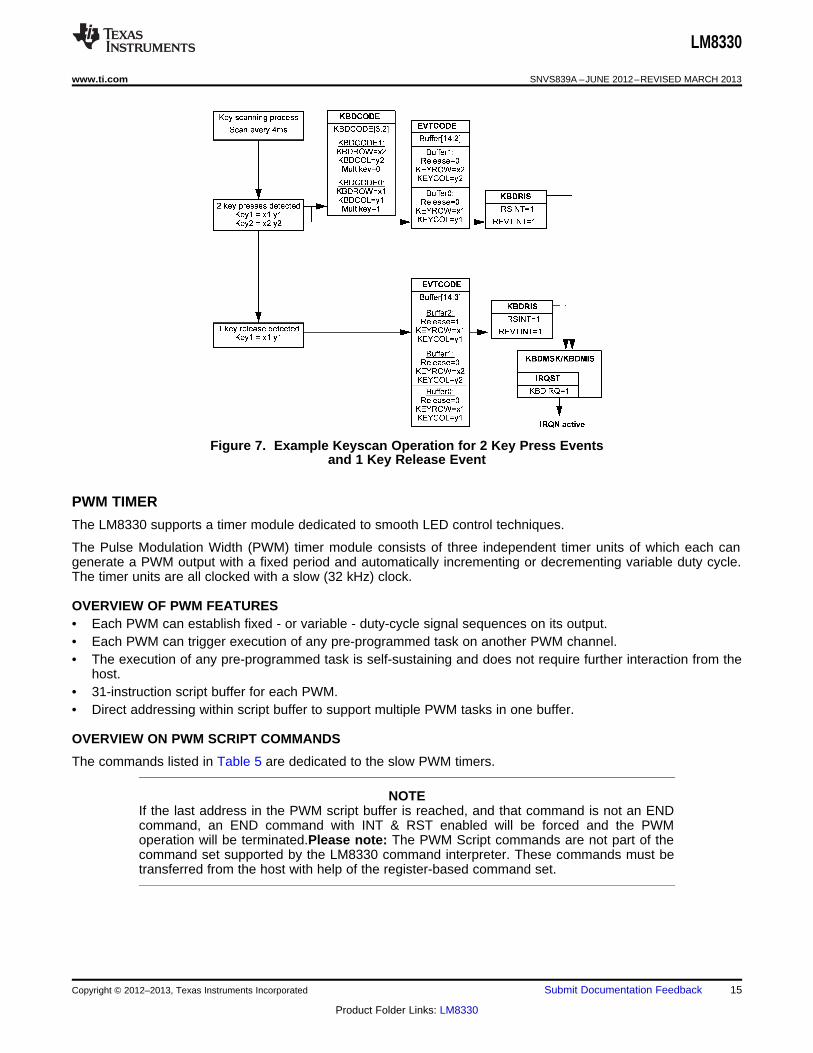
KEYSCAN PROCESS
The LM8330 keyscan functionality is based on a specific scanning procedure performed in a 4ms interval. Oneach scan all assigned key matrix pins are evaluated for state changes.
In case a key event has been identified, the event is stored in the key event FIFO, accessible via the EVTCODEregister. A key event can either be a key press or a key release. In addition, key presses are also stored in theKBDCODE[3:0] registers. As soon as the EVTCODE FIFO includes a event, the device sets the RAW keyboardevent interrupt REVTINT. The RSINT interrupt is set anytime the keyboard status has changed.
Depending on the interrupt masking for the keyboard events (KBDMSK) and the masked interrupt handling(KBDMIS), the pin IRQN will follow the IRQST.KBDIRQ status, which is set as soon as one interrupt in KBDRISis set.
Figure 5 shows the basic flow of a scanning process and which registers are affected.
Figure 5. Example Keyscan Operation for1 Key Press and Release
READING KEYSCAN STATUS BY THE HOST
In order to keep track of the keyscan status, the host either needs to regularly poll the IRQST register or needsto react on the Interrupt signaled by the IRQN pin, in case the ball is configured for interrupt functionality. (SeeGPIO FEATURE CONFIGURATION).
Figure 6 gives an example on which registers to read to get the keyboard events from the LM8330 and how theyinfluence the interrupt event registers. The example is based on the assumption that the LM8330 has indicatedthe keyboard event by the IRQN pin.
Since the interrupt pin has various sources, the host first checks the IRQST register for the interrupt source. IfKBDIRQ is set, the host can check the KBDMIS register to define the exact interrupt source. KBDMIS containsthe masked status of KBDRIS and reflects the source for raising the interrupt pin. The interrupt mask is definedby KBDMSK. The complete status of all pending keyboard interrupts is available in the raw interrupt registerKBDRIS.
After evaluating the interrupt source the host starts reading the EVTCODE or KBDCODE register. In thisexample the host first reads the KBDCODE to get possible key press events and afterwards reads the completeevent list by reading the EVTCODE register until all events are captured (0x7F indicates end of buffer).
Reading KBDCODE clears the RSINT interrupt bit if all keyboards events are emptied. In the same way,REVTINT is cleared in case the EVTCODE FIFO reaches its empty state on read.
Copyright © 2012–2013, Texas Instruments Incorporated Submit Documentation Feedback 13
Product Folder Links: LM8330

LM8330
SNVS839A –JUNE 2012–REVISED MARCH 2013 www.ti.com
The event buffer content and the REVTINT and RELINT (lost event) interrupt bits are also cleared if theKBDIC.EVTIC bit is set.
Interrupt bits in the masked interrupt register KBDMIS follow the masked KBDRIS status.
In order to support efficient Multi-byte reads from EVTCODE, the auto-increment feature is turned off for thisregister. Therefore the host can continuously read the complete EVTCODE buffer by sending one command.
Figure 6. Example Host Reacting toInterrupt for Keypad Event
MULTIPLE KEY PRESSES
The LM8330 supports up to four simultaneous key presses. Any time a single key is pressed KBDCODE0 is setwith the appropriate key code. If a second key is pressed, the key is stored in KBDCODE1 and the MULTIKEYflag of KBDCODE0 is set. Additional key presses are stored in KBDCODE2 and KBDCODE3 accordingly. Thefour registers signal the last multi key press events.
All events are stored in parallel in the EVTCODE register for the complete set of events.
All KBDCODE[3:0] registers are cleared on read.
14 Submit Documentation Feedback Copyright © 2012–2013, Texas Instruments Incorporated
Product Folder Links: LM8330
LM8330
www.ti.com SNVS839A –JUNE 2012–REVISED MARCH 2013
Figure 7. Example Keyscan Operation for 2 Key Press Eventsand 1 Key Release Event
PWM TIMER
The LM8330 supports a timer module dedicated to smooth LED control techniques.
The Pulse Modulation Width (PWM) timer module consists of three independent timer units of which each cangenerate a PWM output with a fixed period and automatically incrementing or decrementing variable duty cycle.The timer units are all clocked with a slow (32 kHz) clock.
OVERVIEW OF PWM FEATURES• Each PWM can establish fixed - or variable - duty-cycle signal sequences on its output.• Each PWM can trigger execution of any pre-programmed task on another PWM channel.• The execution of any pre-programmed task is self-sustaining and does not require further interaction from the
host.• 31-instruction script buffer for each PWM.• Direct addressing within script buffer to support multiple PWM tasks in one buffer.
OVERVIEW ON PWM SCRIPT COMMANDS
The commands listed in Table 5 are dedicated to the slow PWM timers.
NOTEIf the last address in the PWM script buffer is reached, and that command is not an ENDcommand, an END command with INT & RST enabled will be forced and the PWMoperation will be terminated.Please note: The PWM Script commands are not part of thecommand set supported by the LM8330 command interpreter. These commands must betransferred from the host with help of the register-based command set.
Copyright © 2012–2013, Texas Instruments Incorporated Submit Documentation Feedback 15
Product Folder Links: LM8330

LM8330
SNVS839A –JUNE 2012–REVISED MARCH 2013 www.ti.com
Table 5. PWM Script CommandsCommand 15 14 13 12 11 10 9 8 7 6 5 4 3 2 1 0
RAMP 0 PRESCALE STEPTIME SIGN INCREMENT
SET_PWM 0 1 0 PWM VALUE
GO_TO_0
START
BRANCH 1 0 1 LOOPCOUNT ADDR X STEPNUMBER
END 1 1 0 INT RST X
TRIGGER 1 1 1 WAITTRIGGER SENDTRIGGER 0
RAMP Command
A RAMP command will vary the duty cycle of a PWM output in either direction (up or down). The INCREMENTfield specifies the amount of steps for the RAMP. The maximum amount of steps which can be executed withone RAMP Command is 126 which is equivalent to 50%. The SIGN bit field determines the direction of a RAMP(up or down). The STEPTIME field and the PRESCALE bit determine the duration of one step. Based on a 32kHz clock, the minimum time resulting from these options would be 0.49 milliseconds and the maximum time forone step would be 1 second.
Table 6. RAMP Command Bit and Building Fields15 14 13 12 11 10 9 8 7 6 5 4 3 2 1 0
0 PRESCALE STEPTIME SIGN INCREMENT
Table 7. Description of Bit and Building Fields of the RAMP Command
Bit or Field Value Description
0 Divide the 32 kHz clock by 16.PRESCALE
1 Divide the 32 kHz clock by 512.
STEPTIME 1 - 63 Number of prescaled clock cycles per step.
0 Increment RAMP counter.SIGN
1 Decrement RAMP counter.
Number of steps executed by this instruction; a value of 0 functions as a WAITINCREMENT 0 - 126 determined by STEPTIME.
SET_PWM Command
The SET_PWM command does not allow generation of a PWM output with a fixed duty cycle between 0% and100%. This command will set the starting duty cycle MIN SCALE or FULL SCALE (0% or 100%). A RAMPcommand following the SET_PWM command will finally establish the desired duty cycle on the PWM output.
Table 8. SET_PWM Command Bit and Building Fields15 14 13 12 11 10 9 8 7 6 5 4 3 2 1 0
0 1 0 0 0 0 0 0 DUTYCYCLE
Table 9. Description of Bit and Building Fields of the SET_PWM Command
Bit or Field Value Description
0 Duty cycle is 0%.DUTYCYCLE
255 Duty cycle is 100%.
GO_TO_START Ccommand
The GO_TO_START command jumps to the first command in the script command file.
Table 10. GO_TO_START Command Bit and Building Fields15 14 13 12 11 10 9 8 7 6 5 4 3 2 1 0
0
16 Submit Documentation Feedback Copyright © 2012–2013, Texas Instruments Incorporated
Product Folder Links: LM8330

LM8330
www.ti.com SNVS839A –JUNE 2012–REVISED MARCH 2013
BRANCH Command
The BRANCH command jumps to the specified command in the script command file. The branch is executedwith either absolute or relative addressing. In addition, the command gives the option of looping for a specifiednumber of repetitions.
NOTENested loops are not allowed.
Table 11. BRANCH Command Bit and Building Fields15 14 13 12 11 10 9 8 7 6 5 4 3 2 1 0
1 0 1 LOOPCOUNT ADDR X STEPNUMBER
Table 12. Description of Bit and Building Fields of the BRANCH Command
Bit or Field Value Description
0 Loop until a STOP PWM SCRIPT command is issued by the host.LOOPCOUNT
1 - 63 Number of loops to perform.
0 Absolute addressingADDR
1 Relative addressing
Depending on ADDR:STEPNUMBER 0 - 31 ADDR=0: Addr to jump to
ADDR=1: Number of backward steps
TRIGGER Command
Triggers are used to synchronize operations between PWM channels. A TRIGGER command that sends atrigger takes sixteen 32 kHz clock cycles, and a command that waits for a trigger takes at least sixteen 32 kHzclock cycles.
A TRIGGER command that waits for a trigger (or triggers) will stall script execution until the trigger conditions aresatisfied. On trigger it will clear the trigger(s) and continue to the next command.
When a trigger is sent, it is stored by the receiving channel and can only be cleared when the receiving channelexecutes a TRIGGER command that waits for the trigger.
Table 13. TRIGGER Command Bit and Building Fields15 14 13 12 11 10 9 8 7 6 5 4 3 2 1 0
1 1 1 WAITTRIGGER SENDTRIGGER 0
Table 14. Description of Bit and Building Fields
Field Value Description
000xx1 Wait for trigger from channel 0
WAITTRIGGER 000x1x Wait for trigger from channel 1
0001xx Wait for trigger from channel 2
000xx1 Send trigger to channel 0
SENDTRIGGER 000x1x Send trigger to channel 1
0001xx Send trigger to channel 2
END COMMAND
The END command terminates script execution. It will only assert an interrupt to the host if the INT bit is set to'1'.
When the END command is executed, the PWM output will be set to the level defined by PWMCFG.PWMPOLfor this channel. Also, the script counter is reset back to the beginning of the script command buffer.
Copyright © 2012–2013, Texas Instruments Incorporated Submit Documentation Feedback 17
Product Folder Links: LM8330

LM8330
SNVS839A –JUNE 2012–REVISED MARCH 2013 www.ti.com
NOTEIf a PWM channel is waiting for the trigger (last executed command was "TRIGGER"), andthe script execution is halted, then the "END" command can’t be executed because theprevious command is still pending. This is an exception - in this case the IRQ signal willnot be asserted.
Table 15. END Command Bit and Building Fields15 14 13 12 11 10 9 8 7 6 5 4 3 2 1 0
1 1 0 INT RST 0
Table 16. Description of Bit and Building Fields of the END Command
Field Value Description
0 No interrupt will be sent.INT
1 Set TIMRIS.CDIRQ for this PWM channel to notify that program has ended.
0 The PWM Output is set Low.RST
1 The PWM Output is set according to PWMCFG.PWMPOL.
LM8330 REGISTER SET
KEYBOARD REGISTERS AND KEYBOARD CONTROL
Keyboard selection and control registers are mapped in the address range from 0x01 to 0x09. This paragraphdescribes the functions of the associated registers down to the bit level.
KBDSETTLE - Keypad Settle Time Register
Table 17. KBDSETTLE - Keypad Settle Time Register
Register - Name Address Type Register Function
Initial time for keys to settle, before the key-scan process is started. TheKeypad settle time will be imposed under the following conditions:
KBDSETTLE 0x01 R/W a. A wake-up event on the keypad input (if KBDEN=1)b. The MODCTL register bit is written to transition from “halt” to
“operational” mode (if KBDEN=1).
Bit - Name Bit Default Bit Function
The default value 0x80 : 0xBF sets a time target of 12 msec.
Further time targets are as follows:
0xC0 - 0xFF: 16 msec
WAIT[7:0] 7:0 0x80 0x80 - 0xBF: 12 msec
0x40 - 0x7F: 8 msec
0x01 - 0x3F: 4 msec
0x00 : no settle time
KBDBOUNCE - Debounce Time Register
Table 18. KBDBOUNCE - Debounce Time Register
Register - Name Address Type Register Function
KBDBOUNCE 0x02 R/W Time between first detection of key and final sampling of key.
Bit - Name Bit Default Bit Function
18 Submit Documentation Feedback Copyright © 2012–2013, Texas Instruments Incorporated
Product Folder Links: LM8330

LM8330
www.ti.com SNVS839A –JUNE 2012–REVISED MARCH 2013
Table 18. KBDBOUNCE - Debounce Time Register (continued)
Register - Name Address Type Register Function
The default value 0x80 : 0xBF sets a time target of 12 msec.
Further time targets are as follows:
0xC0 - 0xFF: 16 msec
WAIT[7:0] 7:0 0x80 0x80 - 0xBF: 12 msec
0x40 - 0x7F: 8 msec
0x01 - 0x3F: 4 msec
0x00: no debouncing time
KBDSIZE - Set Keypad Size Register
Table 19. KBDSIZE - Set Keypad Size Register
Register - Name Address Type Register Function
KBDSIZE 0x03 R/W Defines the physical keyboard matrix size.
Bit - Name Bit Default Bit Function
Number of rows in the keyboard matrix:
0x0: free all rows to become GPIO, KPX[1:0] used as dedicated key inputsif scanning is enabled by CLKEN.KBEN:ROWSIZE[3:0] 7:4 0x20x1: (illegal value)
0x2 - 0x8: Number of rows in the matrix
Number of columns in the keyboard matrix:
0x0: free all rows to become GPIO, KPY[1:0] used as dedicated key inputsif scanning is enabled by CLKEN.KBENCOLSIZE[3:0] 3:0 0x20x1: (illegal value)
0x2 - 0xC: Number of columns in the matrix
KBDDEDCFG - Dedicated Key Register
Table 20. KBDDEDCFG - Dedicated Key Register
Register - Name Address Type Register Function
Defines if a key is used as a standard keyboard/GPIO pin or whether it isKBDDEDCFG 0x04 R/W used as dedicated key input.
Bit - Name Bit Default Bit Function
Each bit in ROW [7:2] corresponds to ball KPX7 : KPX2.
Bit=0: the dedicated key function applies.ROW[7:2] 15:10 0x3F Bit=1: no dedicated key function is selected. The standard GPIO
functionality applies according to register IOCFG or defined keyboardmatrix.
Each bit in COL [11:10] corresponds to ball KPY11 : KPY10.
Bit=0: the dedicated key function applies.COL[11:10] 9:8 0x03 Bit=1: no dedicated key function is selected. The standard GPIO
functionality applies according to register IOCFG or defined keyboardmatrix.
Each bit in COL [9:2] corresponds to ball KPY9 : KPY2 and can beconfigured individually.
Bit=0: the dedicated key function applies.COL[9:2] 7:0 0xFFBit=1: no dedicated key function is selected. The standard GPIOfunctionality applies according to register IOCFG or defined keyboardmatrix.
Copyright © 2012–2013, Texas Instruments Incorporated Submit Documentation Feedback 19
Product Folder Links: LM8330

LM8330
SNVS839A –JUNE 2012–REVISED MARCH 2013 www.ti.com
KBDRIS - Keyboard Raw Interrupt Status Register
Table 21. KBDRIS - Keyboard Raw Interrupt Status Register
Register - Name Address Type Register Function
KBDRIS 0x06 R Returns the status of stored keyboard interrupts.
Bit - Name Bit Default Bit Function
(reserved) 7:4 (reserved)
Raw event lost interrupt.
More than 16 keyboard events have been detected and caused the eventRELINT 3 0x0buffer to overflow. This bit is cleared by setting bit EVTIC of the KBDICregister.
Raw keyboard event interrupt.REVTINT 2 0x0 At least one key press or key release is in the keyboard event buffer.
Reading from EVTCODE until the buffer is empty will clear this interrupt.
Raw key lost interrupt indicates a lost key-code.
This interrupt is asserted when RSINT has not been cleared uponRKLINT 1 0x0detection of a new key press or key release, or when more than 4 keysare pressed simultaneously.
Raw scan interrupt.
Interrupt generated after keyboard scan, if the keyboard status hasRSINT 0 0x0changed. Reading from KBDCODE until the buffer is empty will clear thisinterrupt.
KBDMIS - Keypad Masked Interrupt Status Register
Table 22. KBDMIS - Keypad Masked Interrupt Status Register
Register - Name Address Type Register Function
Returns the status on masked keyboard interrupts after masking with theKBDMIS 0x07 R KBDMSK register.
Bit - Name Bit Default Bit Functions
(reserved) 7:4 (reserved)
Masked event lost interrupt.
More than 16 keyboard events have been detected and caused the eventMELINT 3 0x0buffer to overflow. This bit is cleared by setting bit EVTIC of the KBDICregister.
Masked keyboard event interrupt.MEVTINT 2 0x0 At least one key press or key release is in the keyboard event buffer.
Reading from EVTCODE until the buffer is empty will clear this interrupt.
Masked key lost interrupt.
Indicates a lost key-code. This interrupt is asserted when RSINT has notMKLINT 1 0x0been cleared upon detection of a new key press or key release, or whenmore than 4 keys are pressed simultaneously.
Masked scan interrupt.
Interrupt generated after keyboard scan, if the keyboard status hasMSINT 0 0x0changed, after masking process. Reading from KDBCODE until the bufferis empty will clear this interrupt.
KBDIC - Keypad Interrupt Clear Register
Table 23. KBDIC - Keypad Interrupt Clear Register
Register - Name Address Default Register Function
KBDIC 0x08 W Setting these bits clears Keypad active Interrupts
Bit - Name Bit Default Bit Function
20 Submit Documentation Feedback Copyright © 2012–2013, Texas Instruments Incorporated
Product Folder Links: LM8330

LM8330
www.ti.com SNVS839A –JUNE 2012–REVISED MARCH 2013
Table 23. KBDIC - Keypad Interrupt Clear Register (continued)
Register - Name Address Default Register Function
Switches off scanning of special function (SF) keys, when keyboard hasno special function layout:
SFOFF 7 0: keyboard layout and SF keys are scanned
1: only keyboard layout is scanned, SF keys are not scanned
(reserved) 6:2 (reserved)
Clear EVTCODE FIFO and corresponding interrupts REVTINT andRELINT by writing a 1 to this bit position.Note: Any key data in the EVTCODE FIFO will be lost when this bit is set;
EVTIC 1 it is the users responsibility to ensure that all key data is read prior toasserting this bit. If a key is pressed while EVTIC is asserted/de-assertedthe EVTCODE FIFO will be updated with only the key release code whenthe key is released.
Clear RSINT and RKLINT interrupt bits by writing a '1' to this bit position.KBDIC 0 Note The KBDCODE registers are not cleared when setting this bit.
KBDMSK - Keypad Interrupt Mask Register
Table 24. KBDMSK - Keypad Interrupt Mask Register
Register - Name Address Type Register Function
Configures masking of keyboard interrupts. Masked interrupts do nottrigger an event on the Interrupt output.
In case the interrupt processes registers KBDCODE[3:0], MSKELINT andKBDMSK 0x09 R/W MSKEINT should be set to '1'. When the Event FIFO is processed,
MSKLINT and MSKSINT should be set. For keyboard polling operations,all bits should be set and the polling operation consists of reading out theIRQST.
Bit - Name Bit Default Bit Function
(reserved) 7:4 (reserved)
0: keyboard event lost interrupt RELINT triggers IRQ lineMSKELINT 3 0x0
1: keyboard event lost interrupt RELINT is masked
0: keyboard event interrupt REVINT triggers IRQ lineMSKEINT 2 0x0
1: keyboard event interrupt REVINT is masked
0: keyboard lost interrupt RKLINT triggers IRQ lineMSKLINT 1 0x1
1: keyboard lost interrupt RKLINT is masked
0: keyboard status interrupt RSINT triggers IRQ lineMSKSINT 0 0x1
1: keyboard status interrupt RSINT is masked
KEYBOARD CODE DETECT REGISTERS
The key code detected by the keyboard scan can be read from the registers KBDCODE0: KBDCODE3. Up to 4keys can be detected simultaneously. Each KBDCODE register includes a bit (MULTIKEY) indicating if anotherkey has been detected.
NOTEReading out all key code registers (KBDCODE0 to KBDCODE3) will automatically resetthe keyboard scan interrupt RSINT the same way as an active write access into bit KBDICof the interrupt clear register does. Reading 0x7F from the KBDCODE0 register meansthat no key was pressed.
Copyright © 2012–2013, Texas Instruments Incorporated Submit Documentation Feedback 21
Product Folder Links: LM8330

LM8330
SNVS839A –JUNE 2012–REVISED MARCH 2013 www.ti.com
KBDCODE0 - Keyboard Code Register 0
Table 25. KBDCODE0 - Keyboard Code Register 0
Register - Name Address Default Register Function
KBDCODE0 0x0B R Holds the row and column information of the first detected key.
Bit - Name Bit Default Bit Function
MULTIKEY 7 0x0 If this bit is 1 another key is available in KBDCODE1 register.
KEYROW[2:0] 6:4 0x7 ROW index of detected key (0 to 7).
Column index of detected (0 to 11, 12 for special function key and 13 & 14KEYCOL[3:0] 3:0 0xF for dedicated KPY key).
KBDCODE1 - Keyboard Code Register 1
Table 26. KBDCODE1 - Keyboard Code Register 1
Register - Name Address Default Register Function
KBDCODE1 0x0C R Holds the row and column information of the second detected key.
Bit - Name Bit Default Bit Function
MULTIKEY 7 0x0 If this bit is 1 another key is available in KBDCODE2 register.
KEYROW[2:0] 6:4 0x7 ROW index of detected key (0 to 7).
Column index of detected key (0 to 11, 12 for special function key and 13KEYCOL[3:0] 3:0 0xF & 14 for dedicated KPY key).
KBDCODE2 - Keyboard Code Register 2
Table 27. KBDCODE2 - Keyboard Code Register 2
Register - Name Address Default Register Function
KBDCODE2 0x0D R Holds the row and column information of the third detected key.
Bit - Name Bit Default Bit Function
MULTIKEY 7 0x0 if this bit is 1 another key is available in KBDCODE3 register.
KEYROW[2:0] 6:4 0x7 ROW index of detected key (0 to 7).
Column index of detected key (0 to 11, 12 for special function key and 13KEYCOL[3:0] 3:0 0xF & 14 for dedicated KPY key).
KBDCODE3 - Keyboard Code Register 3
Table 28. KBDCODE3 - Keyboard Code Register 3
Register - Name Address Default Register Function
KBDCODE3 0x0E R Holds the row and column information of the forth detected key.
Bit - Name Bit Default Bit Function
MULTIKEY 7 0x0 if this bit is set to '1' then more than 4 keys are pressed simultaneously.
KEYROW[2:0] 6:4 0x7 ROW index of detected key (0 to 7).
Column index of detected key (0 to 11, 12 for special function key and 13KEYCOL[3:0] 3:0 0xF & 14 for dedicated KPY key).
22 Submit Documentation Feedback Copyright © 2012–2013, Texas Instruments Incorporated
Product Folder Links: LM8330

LM8330
www.ti.com SNVS839A –JUNE 2012–REVISED MARCH 2013
EVTCODE - Key Event Code Register
Table 29. EVTCODE - Key Event Code Register
Register - Name Address Default Bit Function
With this register a FIFO buffer is addressed storing up to 15 consecutiveevents.
Reading the value 0x7F from this address means that the FIFO buffer isEVTCODE 0x10 R empty. See further details below.
NOTE: Auto increment is disabled on this register. Multi-byte read willalways read from the same address.
Bit - Name Bit Default Bit Function
This bit indicates whether the keyboard event was a key press or a keyrelease event:
RELEASE 7 0x0 0: key was pressed
1: key was released
KEYROW[2:0] 6:4 0x7 Row index of key that is pressed or released.
Column index of detected key that is pressed (0 to 11, 12 for specialKEYCOL[3:0] 3:0 0xF function key or and 13 & 14 for dedicated key) or released.
PWM TIMER CONTROL REGISTERS
The LM8330 provides three host-programmable PWM outputs useful for smooth LED brightness modulation. AllPWM timer control registers are mapped in the range from 0x60 to 0x7F. This paragraph describes the functionsof the associated registers down to the bit level.
TIMCFGx - PWM Timer 0, 1 and 2 Configuration Register
Table 30. TIMCFGx - PWM Timer 0, 1 and 2 Configuration Register
Register - Name Address Type Register Function
TIMCFG0 0x60
TIMCFG1 0x68 R/W This register configures interrupt masking of the associated PWM channel.
TIMCFG2 0x70
Bit - Name Bit Default Bit Function(x = 0, 1 or 2)
Interrupt mask for PWM CYCIRQx (see register TIMRIS):
CYCIRQxMSK 4 0x0 0: interrupt enabled
1: interrupt masked
(reserved) 3:0 0x0 (reserved)
PWMCFGx - PWM Timer 0, 1 and 2 Configuration Control Register
Table 31. PWMCFGx - PWM Timer 0, 1 and 2 Configuration Control Register
Register - Name Address Type Register Function
This register defines interrupt masking and the output behavior for thePWMCFG0 0x61 associated PWM channel.
PWMCFG1 0x69 R/W PGEx is used to start and stop the PWM script execution.
PWMENx sets the PWM output to either reflect the generated pattern orPWMCFG2 0x71 the value configured in PWMPOLx.
Bit - Name Bit Default Bit Function(x = 0, 1 or 2)
Mask for CDIRQ:
CDIRQxMSK 3 0x0 0: CDIRQ enabled
1: CDIRQ disabled/masked
Copyright © 2012–2013, Texas Instruments Incorporated Submit Documentation Feedback 23
Product Folder Links: LM8330

LM8330
SNVS839A –JUNE 2012–REVISED MARCH 2013 www.ti.com
Table 31. PWMCFGx - PWM Timer 0, 1 and 2 Configuration Control Register (continued)
Register - Name Address Type Register Function
Pattern Generator Enable. Start/Stop PWM command processing for thischannel. Script execution is started always from beginning.0: Pattern Generator disabled1: Pattern Generator enabled
PGEx 2 0x0 Notes:1) This bit will be cleared when the PWM completes execution of END
command and END.RST = 1.2) The PWM will complete execution of an active script command if this
bit is set to 0 by the host.
0: PWM disabled. PWM timer output assumes value programmed inPWMPOL.PWMENx 1 0x01: PWM enabled
Off-state of PWM output, when PWMEN = 0:
PWMPOLx 0 0x0 0: PWM off-state is low
1: PWM off-state is high
TIMSWRES - PWM Timer Software Reset Registers
Table 32. TIMSWRES - PWM Timer Software Reset Registers
Register - Name Address Type Register Function
Reset control on all PWM timers.
A reset forces the pattern generator to fetch the first pattern and stops it.Each reset stops all state-machines and timer.TIMSWRES 0x78 WPatterns stored in the pattern configuration register remain unaffected.Interrupts on each timer are not cleared, they need to be cleared writinginto register TIMIC.
Bit - Name Bit Default Bit Function
(reserved) 7:3 (reserved)
Software reset of timer 2:
SWRES2 2 0: no action
1: Software reset on timer 2, needs not to be written back to 0.
Software reset of timer 1
SWRES1 1 0: no action
1: Software reset on timer 1, needs not to be written back to 0.
Software reset of timer 0:
SWRES0 0 0: no action
1: software reset on timer 0, needs not to be written back to '0'.
TIMRIS - PWM Timer Interrupt Status Register
Table 33. TIMRIS - PWM Timer Interrupt Status Register
Register - Name Address Type Register Function
This register returns the raw interrupt status from the PWM timers 0,1 and2.
CYCIRQx - Interrupt from the timers when PWM cycle is complete(applies to the current PWM command residing in the active commandTIMRIS 0x7A R register of a PWM block).
CDIRQx - Interrupt from the pattern generator when PWM pattern code iscomplete (applies to a completed task residing in the script buffer of aPWM block).
Bit - Name Bit Default Bit Functions
(reserved) 7:6 (reserved)
24 Submit Documentation Feedback Copyright © 2012–2013, Texas Instruments Incorporated
Product Folder Links: LM8330

LM8330
www.ti.com SNVS839A –JUNE 2012–REVISED MARCH 2013
Table 33. TIMRIS - PWM Timer Interrupt Status Register (continued)
Register - Name Address Type Register Function
Raw interrupt status for CDIRQ timer2:
CDIRQ2 5 0x0 0: no interrupt pending
1: unmasked interrupt generated
Raw interrupt status for CDIRQ timer1:
CDIRQ1 4 0x0 0: no interrupt pending
1: unmasked interrupt generated
Raw interrupt status for CDIRQ timer0:
CDIRQ0 3 0x0 0: no interrupt pending
1: unmasked interrupt generated
Raw interrupt status for CYCIRQ timer2:
CYCIRQ2 2 0x0 0: no interrupt pending
1: unmasked interrupt generated
Raw interrupt status for CYCIRQ timer1:
CYCIRQ1 1 0x0 0: no interrupt pending
1: unmasked interrupt generated
Raw interrupt status for CYCIRQ timer0:
CYCIRQ0 0 0x0 0: no interrupt pending
1: unmasked interrupt generated
TIMMIS - PWM Timer Masked Interrupt Status Register
Table 34. TIMMIS - PWM Timer Masked Interrupt Status Register
Register - Name Address Type Register Function
This register returns the masked interrupt status from the PWM timers 0, 1and 2. The raw interrupt status (TIMRIS) is masked with the associatedTIMCFGx.CYCIRQxMSK and PWMCFGx.CDIRQxMSK bits to get themasked interrupt status of this register.
CYCIRQ - Interrupt from the timers when PWM cycle is complete (appliesTIMMIS 0x7B R to the current PWM command residing in the active command register of aPWM block).
CDIRQ - Interrupt from the pattern generator when PWM pattern code iscomplete (applies to a completed task residing in the script buffer of aPWM block).
Bit - Name Bit Default Bit Function
(reserved) 7:6 (reserved)
Interrupt after masking, indicates active contribution to the interrupt ball,when set. Status for CDIRQ timer2:
CDIRQ2 5 0x0 0: no interrupt pending
1: interrupt generated
Interrupt after masking, indicates active contribution to the interrupt ball,when set. Status for CDIRQ timer1:
CDIRQ1 4 0x0 0: no interrupt pending
1: interrupt generated
Interrupt after masking, indicates active contribution to the interrupt ball,when set. Status for CDIRQ timer0:
CDIRQ0 3 0x0 0: no interrupt pending
1: interrupt generated
Interrupt after masking, indicates active contribution to the interrupt ball,when set. Status for CYCIRQ timer2:
CYCIRQ2 2 0x0 0: no interrupt pending
1: interrupt generated
Copyright © 2012–2013, Texas Instruments Incorporated Submit Documentation Feedback 25
Product Folder Links: LM8330

LM8330
SNVS839A –JUNE 2012–REVISED MARCH 2013 www.ti.com
Table 34. TIMMIS - PWM Timer Masked Interrupt Status Register (continued)
Register - Name Address Type Register Function
Interrupt after masking, indicates active contribution to the interrupt ball,when set. Status for CYCIRQ timer1:
CYCIRQ1 1 0x0 0: no interrupt pending
1: interrupt generated
Interrupt after masking, indicates active contribution to the interrupt ball,when set. Status for CYCIRQ timer0:
CYCIRQ0 0 0x0 0: no interrupt pending
1: interrupt generated
TIMIC - PWM Timer Interrupt Clear Register
Table 35. TIMIC - PWM Timer Interrupt Clear Register
Register - Name Address Type Register Function
This register clears timer and pattern interrupts.
CYCIRQ - Interrupt from the timers when PWM cycle is complete (appliesto the current PWM command residing in the active command register of a
TIMIC 0x7C W PWM block).
CDIRQ - Interrupt from the pattern generator when PWM pattern code iscomplete (applies to a completed task residing in the script buffer of aPWM block).
Bit - Name Bit Default Bit Function
(reserved) 7:6 (reserved)
Clears interrupt CDIRQ timer2:
CDIRQ2 5 0: no effect
1: interrupt is cleared. Does not need to be written back to 0
Clears interrupt CDIRQ timer1:
CDIRQ1 4 0: no effect
1: interrupt is cleared. Does not need to be written back to 0
Clears interrupt CDIRQ timer0:
CDIRQ0 3 0: no effect
1: interrupt is cleared. Does not need to be written back to 0
Clears interrupt CYCIRQ timer2:
CYCIRQ2 2 0: no effect
1: interrupt is cleared. Does not need to be written back to 0
Clears interrupt CYCIRQ timer1:
CYCIRQ1 1 0: no effect
1: interrupt is cleared. Does not need to be written back to 0
Clears interrupt CYCIRQ timer0:
CYCIRQ0 0 0: no effect
1: interrupt is cleared. Does not need to be written back to 0
PWMWP - PWM Timer Pattern Pointer Register
Table 36. PWMWP - PWM Timer Pattern Pointer Register
Register - Name Address Type Register Function
Pointer to the pattern position inside the configuration register, which willbe overwritten by the next write access to be PWMCFG register.
PWMWP 0x7D R/W NOTE: 1 pattern consists of 2 bytes and not the byte position (low orhigh). It is incremented by 1 every time a full PWMCFG register access(word) is performed.
Bit - Name Bit Default Bit Function
26 Submit Documentation Feedback Copyright © 2012–2013, Texas Instruments Incorporated
Product Folder Links: LM8330

LM8330
www.ti.com SNVS839A –JUNE 2012–REVISED MARCH 2013
Table 36. PWMWP - PWM Timer Pattern Pointer Register (continued)
Register - Name Address Type Register Function
(reserved) 7 0x0 (reserved)
0 ≤ POINTER < 32 : timer0 patterns 0 to 31
32 ≤ POINTER < 64 : timer1 patterns 0 to 31POINTER[6:0] 6:0 0x0
64 ≤ POINTER < 96 : timer2 patterns 0 to 31
96 ≤ POINTER < 128: not valid
PWMCFG - PWM Script Register
Table 37. PWMCFG - PWM Script Register
Register - Name Address Type Register Function
Two-byte pattern storage register for a PWM script command indexed byPWMWP. PWMWP is automatically incremented.
To be applied by two consecutive parameter bytes in one I2C WritePWMCFG 0x7E W Transaction.
NOTE: Auto-increment is disabled on this register. Address will stay at0x7E for each word access.
Bit - Name Bit Default Bit Function
CMD[15:8] 15:8 High byte portion of a PWM script command
CMD[7:0] 7:0 Low byte portion of a PWM script command
INTERFACE CONTROL REGISTERS
The following section describes the functions of special control registers provided for the main controller.
The manufacturer code MFGCODE and the software revision number SWREV tell the main device whichconfiguration file has to be used for this device.
NOTEI2CSA and MFGCODE use the same address. They just differentiate in the access type:
• Write - I2CSA• Read - MFGCODE
I2CSA - I2C-Compatible ACCESS.bus 10-Bit & 7-Bit Slave Address Register
Table 38. I2CSA - I2C-Compatible ACCESS.bus 10-Bit & 7-Bit Slave Address Register
Register - Name Address Type Register Function
I2C-compatible ACCESS.bus Slave Address.I2CSA 0x80 W
The address is internally applied after the next I2C STOP.
Bit - Name Bit Default Bit Function
10-bit & 7-bit address field for the I2C-compatible ACCESS.bus slaveSLAVEADDR[7:1] 7:1 0x44 address (10-bit: upper three bits = 0).
(reserved) 0 (reserved)
MFGCODE - Manufacturer Code Register
Table 39. MFGCODE - Manufacturer Code Register
Register - Name Address Type Register Function
MFGCODE 0x80 R Manufacturer code of the LM8330.
Bit - Name Bit Default Bit Function
MFGBIT 7:0 0x00 8-bit field containing the manufacturer code.
Copyright © 2012–2013, Texas Instruments Incorporated Submit Documentation Feedback 27
Product Folder Links: LM8330

LM8330
SNVS839A –JUNE 2012–REVISED MARCH 2013 www.ti.com
SWREV - Software Revision Register
Table 40. SWREV - Software Revision Register
Register - Name Address Type Register Function
Software revision code of the LM8330.SWREV 0x81 R NOTE: writing the SW revision with the inverted value triggers a reset (see
SWRESET - Software Reset).
Bit - Name Bit Default Bit Function
SWBIT 7:0 0x84 8 - bit field containing the SW Revision number.
SWRESET - Software Reset
Table 41. SWRESET - Software Reset Register
Register - Name Address Type Register Function
Software reset
NOTE: the reset is only applied if the supplied parameter has the invertedSWRESET 0x81 W value as SWBIT.
Reading this register provides the software revision (see SWREV -Software Revision Register).
Bit - Name Bit Default Bit Function
SWBIT 7:0 Reapply inverted value for software reset.
RSTCTRL - System Reset Register
This register allows resetting specific blocks of the LM8330. These bits are not self-clearing and must be writtento a value of '0' to release the block specific reset. All registers associated with the block specific reset will beinitialized to their default value. During an active reset of a module, the LM8330 will not block the access to themodule registers. A read will return the default value, write commands may or may not be ignored. (Refer to eachblock-specific reset bit for additional details.)
Table 42. RSTCTRL - System Reset Register
Register - Name Address Type Register Function
RSTCTRL 0x82 R/W Software reset of specific parts of the LM8330.
Bit - Name Bit Default Bit Function
(reserved) 7:5 (reserved)
Interrupt controller reset. Does not change status on IRQN ball. Onlycontrols IRQ module register. An interrupt status register read when thisbit is set will return a value of 0 even if there is an Interrupt Status bit set.Pending interrupts will be accumulated and held until IRQRST bit isIRQRST 4 0x0released. Any interrupt can be cleared while IRQRST is active:
0: interrupt controller not reset
1: interrupt controller reset
Timer reset for Timers 0, 1, 2:
TIMRST 3 0x0 0: timer not reset
1: timer is reset
(reserved) 2 0x0 (reserved)
Keyboard interface reset:
KBDRST 1 0x0 0: keyboard is not reset
1: keyboard is reset
GPIO reset:
GPIRST 0 0x0 0: GPIO not reset
1: GPIO is reset.
28 Submit Documentation Feedback Copyright © 2012–2013, Texas Instruments Incorporated
Product Folder Links: LM8330

LM8330
www.ti.com SNVS839A –JUNE 2012–REVISED MARCH 2013
RSTINTCLR - Clear NO Init/Power-On Interrupt Register
Table 43. RSTINTCLR - Clear NO Init/Power-On Interrupt Register
Register - Name Address Type Register Function
This register is used to clear the PORIRQ Interrupt. This interrupt is setRSTINTCLR 0x84 W every time the device returns from RESET (either POR, HW or SW
Reset).
Bit - Name Bit Default Bit Function
reserved 7:1 (reserved)
1: Clears the PORIRQ Interrupt signalled in IRQST register.IRQCLR 0
0: is ignored
CLKMODE - Clock Mode Register
Table 44. CLKMODE - Clock Mode Register
Register - Name Address Type Register Function
CLKMODE 0x88 R/W This register controls the current operating mode of the LM8330 device.
Bit - Name Bit Default Bit Function
(reserved) 7:2 (reserved)
Writing to 00 forces the device to immediately enter sleep mode,regardless of any auto-sleep configuration. Reading this bit returns thecurrent operating mode.NOTE: Any active PWM Outputs will be turned off when the LM8330 istransitioned from Operation Mode to Sleep Mode:MODCTL[1:0] 1:0 0x0100: SLEEP Mode
01: Operation Mode
1x: Future modes
CLKEN - Clock Enable Register
Table 45. CLKEN - Clock Enable Register
Register - Name Address Type Register Function
Controls the clock to different functional units. It is used to enable theCLKEN 0x8A R/W functional blocks globally and independently.
Bit - Name Bit Default Bit Function
(reserved) 7:3 (reserved)
PWM Timer 0, 1, 2 clock enable:
TIMEN 2 0x0 0: Timer 0, 1, 2 clock disabled
1: Timer 0, 1, 2 clock enabled.
(reserved) 1 (reserved)
Keyboard clock enable (enables/disables key scan):
KBDEN 0 0x0 0: Keyboard clock disabled
1: Keyboard clock enabled
AUTOSLIP - Auto-sleep Enable Register
Table 46. AUTOSLIP - Auto-sleep Enable Register
Register - Name Address Type Register Function
AUTOSLP 0x8B R/W This register controls the Auto-Sleep function of the LM8330 device.
Bit - Name Bit Default Bit Function
(reserved) 7:1 (reserved)
Copyright © 2012–2013, Texas Instruments Incorporated Submit Documentation Feedback 29
Product Folder Links: LM8330

LM8330
SNVS839A –JUNE 2012–REVISED MARCH 2013 www.ti.com
Table 46. AUTOSLIP - Auto-sleep Enable Register (continued)
Register - Name Address Type Register Function
Enables automatic sleep mode after a defined activity time stored in theAUTOSLPTI register:
ENABLE 0 0x00 1: Enable entering auto-sleep mode
0: Disable entering auto-sleep mode
AUTOSLPTI - Auto-Sleep Time Register
Table 47. AUTOSLPTI - Auto-Sleep Time Register
Register - Name Address Type Register Function
This register defines the activity time. If this time passes without anyAUTOSLPTIL 0x8C R/W processing events then the device enters into sleep-mode, but only ifAUTOSLPTIH 0x8D AUTOSLP.ENABLE bit is set to 1.
Bit - Name Bit Default Bit Function
(reserved) 15:11 (reserved)
Values of UPTIME[10:0] match to multiples of 4ms:0x00: no autosleep, regardless if AUTOSLP.ENABLE is set0x01: 4ms
UPTIME[10:8] 10:8 0x00 0x02: 8msUPTIME[7:0] 7:0 0xFF 0x7A: 500 ms
0xFF: 1020 ms (default after reset)0x100: 1024 ms0x7FF: 8188 ms
IRQST - Interrupt Global Interrupt Status Register
Table 48. IRQST - Interrupt Global Interrupt Status Register
Register - Name Address Type Register Function
Returns the interrupt status from various on-chip function blocks. If any ofIRQST 0x91 R the bits is set and an IRQN line is configured, the IRQN line is asserted
active.
Bit - Name Bit Default Bit Function
Supply failure on VCC.
Also power-on is considered as an initial supply failure. Therefore, afterpower-on, the bit is set:PORIRQ 7 0x10: no failure recorded
1: Failure - device was completely reset and requires re-programming.
Keyboard interrupt (further key selection in keyboard module):
KBDIRQ 6 0x0 0: inactive
1: active
(reserved) 5:4 (reserved)
Timer2 expiry (CDIRQ or CYCIRQ):
TIM2IRQ 3 0x0 0: inactive
1: active
Timer1 expiry (CDIRQ or CYCIRQ):
TIM1IRQ 2 0x0 0: inactive
1: active
Timer0 expiry (CDIRQ or CYCIRQ):
TIM0IRQ 1 0x0 0: inactive
1: active
GPIO interrupt (further selection in GPIO module):
GPIOIRQ 0 0x0 0: inactive
1: active
30 Submit Documentation Feedback Copyright © 2012–2013, Texas Instruments Incorporated
Product Folder Links: LM8330

LM8330
www.ti.com SNVS839A –JUNE 2012–REVISED MARCH 2013
GPIO FEATURE CONFIGURATION
GPIO Feature Mapping
The LM8330 has a flexible I/O structure which allows flexibility in the assignment of different functionality to eachball. This flexibility is implemented in several registers that are used to configure the balls for function (KeypadMatrix, Dedicated Key, GPIO, PWM, or Interrupt). Each ball can also be configured for direction, internal pullresistor, and output buffer type (full, open drain, open source). The functionality of each ball is determinedaccording to the following configuration priority:
In general the following priority is given:1. Keypad2. GPIO/PWM/Interrupt
Each ball that is configured as part of a Keypad Matrix or Dedicated Keypad input will automatically configure theball direction, pull resistor and output buffer type. Any ball not configured as part of the keypad matrix will beavailable as GPIO, PWM or interrupt output (IRQN) and must be configured accordingly.
The configuration for Keypad, PGIO, PWM, or interrupt usages is defined by the following register priority:• 1st Priority: KBDSIZE• 2nd Priority: KBDDEDCFG• 3rd Priority: IOCFG• 4th Priority: GPIODIR/GPIOME/GPIOMS/IOPC
When there is a conflict between any of these registers the ball will be configured according the priority above.Below are several example programming conflicts and the resulting configuration.• If KBDSIZE selects 8x8 matrix, but KBDDEDCFG selects KPX2 as a Dedicated Input Key, the KBDSIZE
takes priority and the ball will be configured as a Keypad Matrix Input.• If KBDSIZE selects 8x8 matrix, but IOPC selects KPX[7:0] pins to have no pullup resistor enabled, the
KBDSIZE takes priority and the pullup resistors will automatically be enabled on all KPX[7:0] pins. Likewise,the KPY[7:0] pins will be automatically configured to have no pullup or pulldown resistor enabled irregardlessof the settings in the IOPC registers since that behavior is required for Keyboard Matrix Outputs (i.e.KBDSIZE has priority).
• When there is a conflict between KBDSIZE settings and the GPIODIR, GPIOMS, or GPIOME settings,KBDSIZE takes priority and the pins selected as Keyboard Matrix pins are automatically configured into theproper direction, pullup/down configuration, and IO buffer configuration consistent with the required operationas matrix pins.
• If the IOCFG register selects a pin to be a PWM output, but the GPIODIR register selects the pin to be aninput, the IOCFG register takes priority and the pin will behave as a PWM output.
Table 49. Ball Configuration Options
Module connectivity
BALL BALLCFGGPIOSEL
0x0 0x1 0x2 0x3 0x4 0x5 0x6 0x7
KPX[7:0] X Keypad Matrix or GPIO [7:0]
KPY[7:0] X Keypad Matrix or GPIO [15:8]
KPY8/0 -KPY8/ GPIO16KPY8 GPIO161 PWM2 (2) -
KPY9/ Reserved (1)KPY9 X PWM1 -GPIO17
KPY10/KPY10 X PWM0 -GPIO18
KPY11/0 PWM2 (2)GPIO19IRQN
1 IRQN
(1) BALLCFG 0x3 thru 0x7 are invalid and can result in indeterminate behavior.(2) PWM2 functionality is mutally exclusive — one pin at a time only (KPY8 or KPY11) depending on interrupt enable Bit 4 of IOCFG.
Copyright © 2012–2013, Texas Instruments Incorporated Submit Documentation Feedback 31
Product Folder Links: LM8330

LM8330
SNVS839A –JUNE 2012–REVISED MARCH 2013 www.ti.com
IOCGF - Input/Output Pin Mapping Configuration Register
Table 50. IOCGF - Input/Output Pin Mapping Configuration Register
Register - Name Address Type Register Function
Configures usage of KPY[11:8] if not used for Keypad. (Refer to Table 49IOCFG 0xA7 W for appropriate BALLCFG setting.)
Bit - Name Bit Default Bit Function
(reserved, set to(reserved) 7:5 (reserved, set to zero)zero)
Configures KPY11 as the IRQN output:
GPIOSEL 4 1= IRQN enabled
0 = BALLCFG Mapping
(reserved) 3 (reserved, set to zero)
BALLCFG 2:0 Select column to configure — refer to Table 49.
IOPC0 - Pull Resistor Configuration Register 0
Table 51. IOPC0 - Pull Resistor Configuration Register 0
Register - Name Address Type Register Function
IOPC0 (1) OxAA R/W Defines the pull resistor configuration for balls KPX[7:0].
Bit - Name Bit Default Bit Function
Resistor enable for KPX7 ball:
00: no pull resistor at ballKPX7PR[1:0] 15:14 0x2
01: pulldown resistor programmed
1x: pullup resistor programmed
Resistor enable for KPX6 ball:
00: no pull resistor at ballKPX6PR[1:0] 13:12 0x2
01: pulldown resistor programmed
1x: pullup resistor programmed
Resistor enable for KPX5 ball:
00: no pull resistor at ballKPX5PR[1:0] 11:10 0x2
01: pulldown resistor programmed
1x: pullup resistor programmed
Resistor enable for KPX4 ball:
00: no pull resistor at ballKPX4PR[1:0] 9:8 0x2
01: pulldown resistor programmed
1x: pullup resistor programmed
Resistor enable for KPX3 ball:
00: no pull resistor at ballKPX3PR[1:0] 7:6 0x2
01: pulldown resistor programmed
1x: pullup resistor programmed
Resistor enable for KPX2 ball:
00: no pull resistor at ballKPX2PR[1:0] 5:4 0x2
01: pulldown resistor programmed
1x: pullup resistor programmed
Resistor enable for KPX1 ball:
00: no pull resistor at ballKPX1PR[1:0] 3:2 0x2
01: pulldown resistor programmed
1x: pullup resistor programmed
(1) Written values of 0x2 and 0x3 will always be read back as 0x3.
32 Submit Documentation Feedback Copyright © 2012–2013, Texas Instruments Incorporated
Product Folder Links: LM8330

LM8330
www.ti.com SNVS839A –JUNE 2012–REVISED MARCH 2013
Table 51. IOPC0 - Pull Resistor Configuration Register 0 (continued)
Register - Name Address Type Register Function
Resistor enable for KPX0 ball:
00: no pull resistor at ballKPX0PR[1:0] 1:0 0x2
01: pulldown resistor programmed
1x: pullup resistor programmed
IOPC1 - Pull Resistor Configuration Register 1
Table 52. IOPC1 - Pull Resistor Configuration Register 1
Register - Name Address Type Register Function
IOPC1 (1) 0xAC R/W Defines the pull resistor configuration for balls KPY[7:0].
Bit - Name Bit Default Bit Function
Resistor enable for KPY7 ball:
00: no pull resistor at ballKPY7PR[1:0] 15:14 0x1
01 :pulldown resistor programmed
1x: pullup resistor programmed
Resistor enable for KPY6 ball:
00: no pull resistor at ballKPY6PR[1:0] 13:12 0x1
01: pulldown resistor programmed
1x: pullup resistor programmed
Resistor enable for KPY5 ball:
00: no pull resistor at ballKPY5PR[1:0] 11:10 0x1
01: pulldown resistor programmed
1x: pullup resistor programmed
Resistor enable for KPY4 ball:
00: no pull resistor at ballKPY4PR[1:0] 9:8 0x1
01: pulldown resistor programmed
1x: pullup resistor programmed
Resistor enable for KPY3 ball:
00: no pull resistor at ballKPY3PR[1:0] 7:6 0x1
01: pulldown resistor programmed
1x: pullup resistor programmed
Resistor enable for KPY2 ball:
00: no pull resistor at ballKPY2PR[1:0] 5:4 0x1
01: pulldown resistor programmed
1x: pullup resistor programmed
Resistor enable for KPY1 ball:
00: no pull resistor at ballKPY1PR[1:0] 3:2 0x1
01: pulldown resistor programmed
1x: pullup resistor programmed
Resistor enable for KPY0 ball:
00: no pull resistor at ballKPY0PR[1:0] 1:0 0x1
01: pulldown resistor programmed
1x: pullup resistor programmed
(1) Written values of 0x2 and 0x3 will always be read back as 0x3.
Copyright © 2012–2013, Texas Instruments Incorporated Submit Documentation Feedback 33
Product Folder Links: LM8330

LM8330
SNVS839A –JUNE 2012–REVISED MARCH 2013 www.ti.com
IOPC2 - Pull Resistor Configuration Register 2
Table 53. IOPC2 - Pull Resistor Configuration Register 2
Register - Name Address Type Register Function
IOPC2 (1) 0xAE R/W Defines the pull resistor configuration for balls KPY[11:8].
Bit - Name Bit Default Bit Function
(reserved) 15:8 0x5A (reserved)
Resistor enable for KPY11 ball:
00: no pull resistor at ballKPY11PR[1:0] 7:6 0x0
01: pulldown resistor programmed
1x: pullup resistor programmed
Resistor enable for KPY10 ball:
00: no pull resistor at ballKPY10PR[1:0] 5:4 0x1
01 pulldown resistor programmed
1x: pullup resistor programmed
Resistor enable for KPY9 ball:
00: no pull resistor at ballKPY9PR[1:0] 3:2 0x1
01: pulldown resistor programmed
1x: pullup resistor programmed
Resistor enable for KPY8 ball:
00: no pull resistor at ballKPY8PR[1:0] 1:0 0x1
01: pulldown resistor programmed
1x: pullup resistor programmed
(1) Written values of 0x2 and 0x3 will always be read back as 0x3.
GPIOOME0 - GPIO Open Drain Mode Enable Register 0
Table 54. GPIOOME0 - GPIO Open Drain Mode Enable Register 0
Register - Name Address Type Register Function
Configures KPX[7:0] for Open Drain or standard output functionality. TheGPIOOME0 0xE0 R/W Open Drain drive source is configured by GPIOOMS0.
Bit - Name Bit Default Bit Function
Open Drain Enable on KPX[7:0]:
KPX[7:0]ODE 7:0 0x0 0: full buffer
1: open drain functionality
GPIOOMS0 - GPIO Open Drain Mode Select Register 0
Table 55. GPIOOMS0 - GPIO Open Drain Mode Select Register 0
Register - Name Address Type Register Function
Configures the Open Drain drive source on KPX[7:0] if selected byGPIOOMS0 0xE1 R/W GPIOOME0.
Bit - Name Bit Default Bit Function
0: Only nmos transistor is active in output driver stage. Output can bedriven to GND or Hi-Z.
KPX[7:0]ODM 7:0 0x01: Only pmos transistor is active in output driver stage. Output can bedriven to VCC or Hi-Z.
34 Submit Documentation Feedback Copyright © 2012–2013, Texas Instruments Incorporated
Product Folder Links: LM8330

LM8330
www.ti.com SNVS839A –JUNE 2012–REVISED MARCH 2013
GPIOOME1 - GPIO Open Drain Mode Enable Register 1
Table 56. GPIOOME1 - GPIO Open Drain Mode Enable Register 1
Register - Name Address Type Register Function
Configures KPY[7:0] for Open Drain or standard output functionality. TheGPIOOME1 0xE2 R/W Open Drain drive source is configured by GPIOOMS1.
Bit - Name Bit Default Bit Function
Open Drain Enable on KPY[7:0]
KPY[7:0]ODE 7:0 0x0 0: full buffer
1: open drain functionality
GPIOOMS1 - GPIO Open Drain Mode Select Register 1
Table 57. GPIOOMS1 - GPIO Open Drain Mode Select Register 1
Register - Name Address Type Register Function
Configures the Open Drain drive source on KPY[7:0] if selected byGPIOOMS1 0xE3 R/W GPIOOME1.
Bit - Name Bit Default Bit Function
0: Only nmos transistor is active in output driver stage. Output can bedriven to GND or Hi-Z.
KPY[7:0]ODM 7:0 0x01: Only pmos transistor is active in output driver stage. Output can bedriven to VCC or Hi-Z.
GPIOOME2 - GPIO Open Drain Mode Enable Register 2
Table 58. GPIOOME2 - GPIO Open Drain Mode Enable Register 2
Register - Name Address Type Register Function
Configures KPY[11:8] for Open Drain or standard output functionality. TheGPIOOME2 0xE4 R/W Open Drain drive source is configured by GPIOOMS2.
Bit - Name Bit Default Bit Function
(reserved) 7:4 0x0 (reserved)
Open Drain Enable on KPY[11:8]:
0: full bufferKPY[11:8]ODE 3:0 0x81: open drain functionalityNote: IRQN ball defaults to Open Drain Mode Enable after reset.
GPIOOMS2 - GPIO Open Drain Mode Select Register 2
Table 59. GPIOOMS2 - GPIO Open Drain Mode Select Register 2
Register - Name Address Type Register Function
Configures the Open Drain drive source on KPY[11:8] if selected byGPIOOMS2 0xE5 R/W GPIOOME2.
Bit - Name Bit Default Bit Function
(reserved 7:4 (reserved)
0: Only nmos transistor is active in output driver stage. Output can bedriven to GND or Hi-Z.
KPY[11:8]ODM 3:0 0x01: Only pmos transistor is active in output driver stage. Output can bedriven to VCC or Hi-Z.
Copyright © 2012–2013, Texas Instruments Incorporated Submit Documentation Feedback 35
Product Folder Links: LM8330

LM8330
SNVS839A –JUNE 2012–REVISED MARCH 2013 www.ti.com
GPIO DATA INPUT/OUTPUT
GPIOPDATA0 - GPIO Data Register 0
Table 60. GPIOPDATA0 - GPIO Data Register 0
Register - Name Address Type Register Function
This register controls GPIO Data & Mask on KPX[7:0].
If one I/O is defined as output (see Table 63), the values written to thisGPIODATA0 0xC0 R/W register are masked with MASK and then applied to the associated pin.
Any I/O defined as an input (see Table 63) will return the value of theassociated pin regardless of the MASK value when read.
Bit - Name Bit Default Bit Function
Mask Bits for KPX[7:0] when configured as GPIO Output:1: output is not maskedKPX[7:0]MASK 15:8 0x00: output is masked (unchanged)
KPX[7:0] Pin State when configured as GPIO:KPX[7:0] 7:0 0xFC WRITE: Pin State = DATA if not Masked
READ: DATA = Current Pin State
GPIOPDATA1 - GPIO Data Register 1
Table 61. GPIOPDATA1 - GPIO Data Register 1
Register - Name Address Type Register Function
This register controls GPIO Data & Mask on KPY[7:0].
If any I/O is defined as output (see Table 64), the value written to thisGPIODATA1 0xC2 R/W register are masked with MASK and then applied to the associated pin.
Any I/O defined as an input (see Table 64) will return the value of theassociated pin regardless of the MASK value when read.
Bit - Name Bit Default Bit Function
Mask Bits for KPY[7:0] when configured as GPIO Output:
KPY[7:0]MASK 15:8 0x0 1: output is not masked
0: output is masked (unchanged)
KPY[7:0] Pin State when configured as GPIO:KPY[7:0] 7:0 0x00 WRITE: Pin State = DATA if not Masked
READ: DATA = Current Pin State
GPIOPDATA2 - GPIO Data Register 2
Table 62. GPIOPDATA2 - GPIO Data Register 2
Register - Name Address Type Register Function
This register controls GPIO Data & Mask on KPY[11:8].
If any I/O is defined as an output (see Table 65) the value written to thisGPIODATA2 0xC4 R/W register is masked with MASK and then applied to the associated pin.
Any I/O defined as an input (see Table 65) will return the value of theassociated pin regardless of the MASK value when read.
Bit - Name Bit Default Bit Function
36 Submit Documentation Feedback Copyright © 2012–2013, Texas Instruments Incorporated
Product Folder Links: LM8330

LM8330
www.ti.com SNVS839A –JUNE 2012–REVISED MARCH 2013
Table 62. GPIOPDATA2 - GPIO Data Register 2 (continued)
Register - Name Address Type Register Function
(reserved) 15:12 0x0 (reserved)
Mask Status for KPY[11:8] when enabled as GPIO:
KPY[11:8] 11:8 0x0 1: Output is not masked
0: Output is masked.
reserved 7:4 0x0 (reserved)
KPY [11:8] Pin State when configured as GPIO :KPY[11:8]DATA 3:0 0x0 WRITE: Pin State = DATA if not Masked
READ: DATA = Current Pin State
GPIOPDIR0 - GPIO Port Direction Register 0
Table 63. GPIOPDIR0 - GPIO Port Direction Register 0
Register - Name Address Type Register Function
GPIODIR0 0xC6 R/W Port direction for KPX[7:0].
Bit - Name Bit Default Bit Function
Direction bits for KPX[7:0]:
KPX[7:0]DIR 7:0 0x00 0: input mode
1: output mode
GPIOPDIR1 - GPIO Port Direction Register 1
Table 64. GPIOPDIR1 - GPIO Port Direction Register 1
Register - Name Address Type Register Function
GPIODIR1 0xC7 R/W Port direction for KPY[7:0]
Bit - Name Bit Default Bit Function
Direction bits for KPY[7:0]:
KPY[7:0]DIR 7:0 0x00 0: input mode
1: output mode
GPIOPDIR2 - GPIO Port Direction Register 2
Table 65. GPIOPDIR2 - GPIO Port Direction Register 2
Register - Name Address Type Register Function
GPIODIR2 0xC8 R/W Port direction for KPY[11:8]:
Bit - Name Bit Default Bit Function
(reserved) 7:4 (reserved)
Direction bits for KPY[11:8]
KPY[11:8]DIR 3:0 0x08 0: input mode
1: output mode
GPIO INTERRUPT CONTROL
GPIOIS0 - Interrupt Sense Configuration Register 0
Table 66. GPIOIS0 - Interrupt Sense Configuration Register 0
Register - Name Address Type Register Function
GPIOIS0 0xC9 R/W Interrupt type on KPX[7:0].
Bit - Name Bit Default Bit Function
Copyright © 2012–2013, Texas Instruments Incorporated Submit Documentation Feedback 37
Product Folder Links: LM8330

LM8330
SNVS839A –JUNE 2012–REVISED MARCH 2013 www.ti.com
Table 66. GPIOIS0 - Interrupt Sense Configuration Register 0 (continued)
Register - Name Address Type Register Function
Interrupt type bits for KPX[7:0]:
KPX[7:0]IS 7:0 0x0 0: edge sensitive interrupt
1: level sensitive interrupt
GPIOIS1 - Interrupt Sense Configuration Register 1
Table 67. GPIOIS1 - Interrupt Sense Configuration Register 1
Register - Name Address Type Register Function
GPIOIS1 0xCA R/W Interrupt type on KPY[7:0]
Bit - Name Bit Default Bit Function
Interrupt type bits for KPY[7:0]:
KPY[7:0]IS 7:0 0x0 0: edge sensitive interrupt
1: level sensitive interrupt
GPIOIS2 - Interrupt Sense Configuration Register 2
Table 68. GPIOIS2 - Interrupt Sense Configuration Register 2
Register - Name Address Type Register Function
GPIOIS2 0xCB R/W Interrupt type on KPY[11:8]
Bit - Name Bit Default Bit Function
(reserved) 7:4 (reserved)
Interrupt type bits for KPY[11:8]:
KPY[11:8]IS 3:0 0x0 0: edge sensitive interrupt
1: level sensitive interrupt
GPIOIBE0 - GPIO Interrupt Edge Configuration Register 0
Table 69. GPIOIBE0 - GPIO Interrupt Edge Configuration Register 0
Register - Name Address Type Register Function
Defines whether an interrupt on KPX[7:0] is triggered on either edge or onGPIOIBE0 0xCC R/W a single edge. See Table 72 for the edge configuration.
Bit - Name Bit Default Bit Function
Interrupt both edges bits for KPX[7:0]:
KPX[7:0]IBE 7:0 0x0 0: interrupt generated at the active edge
1: interrupt generated after either edge.
GPIOIBE1 - GPIO Interrupt Edge Configuration Register 1
Table 70. GPIOIBE1 - GPIO Interrupt Edge Configuration Register 1
Register - Name Address Type Register Function
Defines whether an interrupt on KPY[7:0] is triggered on either edge or onGPIOIBE1 0xCD R/W a single edge. See Table 73 for the edge configuration.
Bit - Name Bit Default Bit Function
Interrupt both edges bits for KPY[7:0]:
KPY[7:0]IBE 7:0 0x0 0: interrupt generated at the active edge.
1: interrupt generated after either edge.
38 Submit Documentation Feedback Copyright © 2012–2013, Texas Instruments Incorporated
Product Folder Links: LM8330

LM8330
www.ti.com SNVS839A –JUNE 2012–REVISED MARCH 2013
GPIOIBE2 - GPIO Interrupt Edge Configuration Register 2
Table 71. GPIOIBE2 - GPIO Interrupt Edge Configuration Register 2
Register - Name Address Type Register Function
Defines whether an interrupt on KPY[11:8] was triggered on either edge orGPIOIBE2 0xCE R/W on a single edge. See Table 74 for the edge configuration.
Bit - Name Bit Default Bit Function
(reserved 7:4 (reserved)
Interrupt both edges bits for KPY[11:8]:
KPY[11:8]IBE 3:0 0x0 0: interrupt generated at the active edge.
1: interrupt generated after either edge.
GPIOIEV0 - GPIO Interrupt Edge Select Register 0
Table 72. GPIOIEV0 - GPIO Interrupt Edge Select Register 0
Register - Name Address Type Register Function
GPIOIEV0 0xCF R/W Select Interrupt edge for KPX[7:0].
Bit - Name Bit Default Bit Function
Interrupt edge select from KPX[7:0]:
KPX[7:0]EV 7:0 0xFF 0: interrupt at low level or falling edge
1: interrupt at high level or rising edge
GPIOIEV1 - GPIO Interrupt Edge Select Register 1
Table 73. GPIOIEV1 - GPIO Interrupt Edge Select Register 1
Register - Name Address Type Register Function
GPIOIEV1 0xD0 R/W Select Interrupt edge for KPY[7:0].
Bit - Name Bit Default Bit Function
Interrupt edge select from KPY[7:0]:
KPY[7:0]EV 7:0 0xFF 0: interrupt at low level or falling edge
1: interrupt at high level or rising edge
GPIOIEV2 - GPIO Interrupt Edge Select Register 2
Table 74. GPIOIEV2 - GPIO Interrupt Edge Select Register 2
Register - Name Address Type Register Function
GPIOIEV2 0xD1 R/W Select Interrupt edge for KPY[11:8].
Bit - Name Bit Default Bit Function
(reserved) 7:4 (reserved)
Interrupt edge select from KPY[11:8]:
KPY[11:8]EV 3:0 0xFF 0: interrupt at low level or falling edge
1: interrupt at high level or rising edge
GPIOIE0 - GPIO Interrupt Enable Register 0
Table 75. GPIOIE0 - GPIO Interrupt Enable Register 0
Register - Name Address Type Register Function
GPIOIE0 0xD2 R/W Enable/disable interrupts on KPX[7:0].
Bit - Name Bit Default Bit Function
Copyright © 2012–2013, Texas Instruments Incorporated Submit Documentation Feedback 39
Product Folder Links: LM8330

LM8330
SNVS839A –JUNE 2012–REVISED MARCH 2013 www.ti.com
Table 75. GPIOIE0 - GPIO Interrupt Enable Register 0 (continued)
Register - Name Address Type Register Function
Interrupt enable on KPX[7:0]:
KPX[7:0]IE 7:0 0x0 0: disable interrupt
1: enable interrupt
GPIOIE1 - GPIO Interrupt Enable Register 1
Table 76. GPIOIE1 - GPIO Interrupt Enable Register 1
Register - Name Address Type Register Function
GPIOIE1 0xD3 R/W Enable/disable interrupts on KPY[7:0].
Bit - Name Bit Default Bit Function
Interrupt enable on KPY[7:0]:
KPY[7:0]IE 7:0 0x0 0: disable interrupt
1: enable interrupt
GPIOIE2 - GPIO Interrupt Enable Register 2
Table 77. GPIOIE2 - GPIO Interrupt Enable Register 2
Register - Name Address Type Register Function
GPIOIE2 0xD4 R/W Enable/disable interrupts on KPY[11:8].
Bit - Name Bit Default Bit Function
(reserved) 7:4 (reserved)
Interrupt enable on KPY[11:8]:
KPY[11:8]IE 3:0 0x0 0: disable interrupt
1: enable interrupt
GPIOIC0 - GPIO Clear Interrupt Register 0
Table 78. GPIOIC0 - GPIO Clear Interrupt Register 0
Register - Name Address Type Register Function
GPIOIC0 0xDC W Clears the interrupt on KPX[7:0].
Bit - Name Bit Default Bit Function
Clear Interrupt on KPX[7:0]:
KPX[7:0]IC 7:0 0: no effect
1: Clear corresponding interrupt
GPIOIC1 - GPIO Clear Interrupt Register 1
Table 79. GPIOIC1 - GPIO Clear Interrupt Register 1
Register - Name Address Type Register Function
GPIOIC1 0xDD W Clears the interrupt on KPY[7:0].
Bit - Name Bit Default Bit Function
Clear Interrupt on KPY[7:0]:
KPY[7:0]IC 7:0 0: no effect
1: Clear corresponding interrupt
40 Submit Documentation Feedback Copyright © 2012–2013, Texas Instruments Incorporated
Product Folder Links: LM8330

LM8330
www.ti.com SNVS839A –JUNE 2012–REVISED MARCH 2013
GPIOIC2 - GPIO Clear Interrupt Register 2
Table 80. GPIOIC2 - GPIO Clear Interrupt Register 2
Register - Name Address Type Register Function
GPIOIC2 0xDE W Clears the interrupt on KPY[11:8].
Bit - Name Bit Default Bit Function
(reserved) 7:4 (reserved)
Clear Interrupt on KPY[11:8]:
KPY[11:8]IC 3:0 0: no effect
1: Clear corresponding interrupt
GPIO INTERRUPT STATUS
GPIORIS0 - Raw Interrupt Status Register 0
Table 81. GPIORIS0 - Raw Interrupt Status Register 0
Register - Name Address Type Register Function
GPIORIS0 0xD6 R Raw interrupt status on KPX[7:0]
Bit - Name Bit Default Bit Function
Raw Interrupt status data on KPX[7:0]:
KPX[7:0]RIS 7:0 0x0 0: no interrupt condition at GPIO
1: interrupt condition at GPIO
GPIORIS1 - Raw Interrupt Status Register 1
Table 82. GPIORIS1 - Raw Interrupt Status Register 1
Register - Name Address Type Register Function
GPIORIS1 0xD7 R Raw interrupt status on KPY[7:0].
Bit - Name Bit Default Bit Function
Raw Interrupt status data on KPY[7:0]:
KPY[7:0]RIS 7:0 0x0 0: no interrupt condition at GPIO
1: interrupt condition at GPIO
GPIORIS2 - Raw Interrupt Status Register 2
Table 83. GPIORIS2 - Raw Interrupt Status Register 2
Register - Name Address Type Register Function
GPIORIS2 0xD8 R Raw interrupt status on KPY[11:8].
Bit - Name Bit Default Bit Function
(reserved) 7:4 (reserved)
Raw Interrupt status data on KPY[11:8]:
KPY[11:8]RIS 3:0 0x0 0: no interrupt condition at GPIO
1: interrupt condition at GPIO
GPIOMIS0 - Masked Interrupt Status Register 0
Table 84. GPIOMIS0 - Masked Interrupt Status Register 0
Register - Name Address Type Register Function
GPIOMIS0 0xD9 R Masked interrupt status on KPX[7:0].
Bit - Name Bit Default Bit Function
Copyright © 2012–2013, Texas Instruments Incorporated Submit Documentation Feedback 41
Product Folder Links: LM8330

LM8330
SNVS839A –JUNE 2012–REVISED MARCH 2013 www.ti.com
Table 84. GPIOMIS0 - Masked Interrupt Status Register 0 (continued)
Register - Name Address Type Register Function
Masked Interrupt status data on KPX[7:0]:
KPX[7:0]MIS 7:0 0x0 0: no interrupt contribution from GPIO
1: interrupt GPIO is active
GPIOMIS1 - Masked Interrupt Status Register 1
Table 85. GPIOMIS1 - Masked Interrupt Status Register 1
Register - Name Address Type Register Function
GPIOMIS1 0xDA R Masked interrupt status on KPY[7:0].
Bit - Name Bit Default Bit Function
Masked Interrupt status data on KPY[7:0]:
KPY[7:0]MIS 7:0 0x0 0: no interrupt contribution from GPIO
1: interrupt GPIO is active
GPIOMIS2 - Masked Interrupt Status Register 2
Table 86. GPIOMIS2 - Masked Interrupt Status Register 2
Register - Name Address Type Register Function
GPIOMIS2 0xDB R Masked interrupt status on KPY[11:8].
Bit - Name Bit Default Bit Function
(reserved) 7:4 (reserved)
Masked Interrupt status data on KPY[11:8]:
KPY[11:8]MIS 3:0 0x0 0: no interrupt contribution from GPIO
1: interrupt GPIO is active
GPIO WAKE-UP CONTROL
GPIOWAKE0 - GPIO Wake-Up Register 0
Table 87. GPIOWAKE0 - GPIO Wake-Up Register 0
Register - Name Address Type Register Function
Configures wake-up conditions for KPX[7:0].GPIOWAKE0 0xE9 R/W Each bit corresponds to a ball. When a bit is set, the corresponding ball
contributes to wakeup from auto-sleep mode.
Bit - Name Bit Default Bit Function
Wake up from auto sleep on KPY[7:0]KPX[7:0]WAKE 7:0 0x0 0: wake up from auto sleep disabled
1: wake up from auto sleep enabled
GPIOWAKE1 - GPIO Wake-Up Register 1
Table 88. GPIOWAKE1 - GPIO Wake-Up Register 1
Register - Name Address Type Register Function
Configures wake-up conditions for KPY[7:0].GPIOWAKE1 0xEA R/W Each bit corresponds to a ball. When a bit is set, the corresponding ball
contributes to wakeup from auto-sleep mode.
Bit - Name Bit Default Bit Function
Wake up from Auto sleep on KPY[7:0]KPY[7:0]WAKE 7:0 0x0 0: wake up from auto sleep disabled
1: wake up from auto sleep enabled
42 Submit Documentation Feedback Copyright © 2012–2013, Texas Instruments Incorporated
Product Folder Links: LM8330
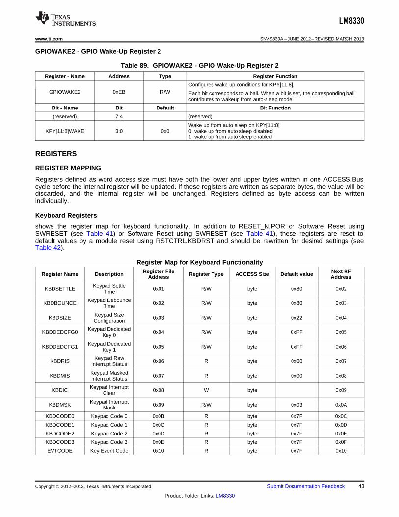
LM8330
www.ti.com SNVS839A –JUNE 2012–REVISED MARCH 2013
GPIOWAKE2 - GPIO Wake-Up Register 2
Table 89. GPIOWAKE2 - GPIO Wake-Up Register 2
Register - Name Address Type Register Function
Configures wake-up conditions for KPY[11:8].GPIOWAKE2 0xEB R/W Each bit corresponds to a ball. When a bit is set, the corresponding ball
contributes to wakeup from auto-sleep mode.
Bit - Name Bit Default Bit Function
(reserved) 7:4 (reserved)
Wake up from auto sleep on KPY[11:8]KPY[11:8]WAKE 3:0 0x0 0: wake up from auto sleep disabled
1: wake up from auto sleep enabled
REGISTERS
REGISTER MAPPING
Registers defined as word access size must have both the lower and upper bytes written in one ACCESS.Buscycle before the internal register will be updated. If these registers are written as separate bytes, the value will bediscarded, and the internal register will be unchanged. Registers defined as byte access can be writtenindividually.
Keyboard Registers
shows the register map for keyboard functionality. In addition to RESET_N,POR or Software Reset usingSWRESET (see Table 41) or Software Reset using SWRESET (see Table 41), these registers are reset todefault values by a module reset using RSTCTRL.KBDRST and should be rewritten for desired settings (seeTable 42).
Register Map for Keyboard FunctionalityRegister File Next RFRegister Name Description Register Type ACCESS Size Default valueAddress Address
Keypad SettleKBDSETTLE 0x01 R/W byte 0x80 0x02Time
Keypad DebounceKBDBOUNCE 0x02 R/W byte 0x80 0x03Time
Keypad SizeKBDSIZE 0x03 R/W byte 0x22 0x04Configuration
Keypad DedicatedKBDDEDCFG0 0x04 R/W byte 0xFF 0x05Key 0
Keypad DedicatedKBDDEDCFG1 0x05 R/W byte 0xFF 0x06Key 1
Keypad RawKBDRIS 0x06 R byte 0x00 0x07Interrupt Status
Keypad MaskedKBDMIS 0x07 R byte 0x00 0x08Interrupt Status
Keypad InterruptKBDIC 0x08 W byte 0x09Clear
Keypad InterruptKBDMSK 0x09 R/W byte 0x03 0x0AMask
KBDCODE0 Keypad Code 0 0x0B R byte 0x7F 0x0C
KBDCODE1 Keypad Code 1 0x0C R byte 0x7F 0x0D
KBDCODE2 Keypad Code 2 0x0D R byte 0x7F 0x0E
KBDCODE3 Keypad Code 3 0x0E R byte 0x7F 0x0F
EVTCODE Key Event Code 0x10 R byte 0x7F 0x10
Copyright © 2012–2013, Texas Instruments Incorporated Submit Documentation Feedback 43
Product Folder Links: LM8330

LM8330
SNVS839A –JUNE 2012–REVISED MARCH 2013 www.ti.com
PWM Timer Registers
shows the register map for PWM Timer functionality. In addition to RESET_N, POR and software reset usingSWRESET (see Table 41), these registers are reset to default values by a module reset usingRSTCTRL.TIMRST (see RSTCTRL - System Reset Register).
Register Map for PWM Timer FunctionalityRegister File Next RFRegister Name Description Register Type ACCESS Size Default valueAddress Address
PWM TimerTIMCFG0 0x60 R/W byte 0x00 0x61Configuration 0
PWM ConfigurationPWMCFG0 0x61 R/W byte 0x00 0x620
PWM TimerTIMCFG1 0x68 R/W byte 0x00 0x69Configuration 1
PWM ConfigurationPWMCFG1 0x69 R/W byte 0x00 0x6A1
PWM TimerTIMCFG2 0x70 R/W byte 0x00 0x71Configuration 2
PWM ConfigurationPWMCFG2 0x71 R/W byte 0x00 0x722
PWM Timer SWTIMSWRES 0x78 W byte 0x79Reset
PWM TimerTIMRIS 0x7A R byte 0x00 0x7BInterrupt Status
PWM TimerTIMMIS 0x7B R byte 0x00 0x7CMasked Int. Status
Timer InterruptTIMIC 0x7C W byte 0x7DClear
PWM CommandPWMWP 0x7D R/W byte 0x00 0x7EWrite Pointer
PWM CommandPWMCFG 0x7E W word 0x7FScript
System Registers
shows the register map for general system registers. These registers are not affected by any of the moduleresets addressed by RSTCTRL (see Table 42). These registers can only be reset to default values by a GlobalCall Reset (see GENERAL CALL RESET) or by a complete Software Reset using SWRESET (see Table 41).
Register Map for System Control FunctionalityRegister Name Description Register File Register Type ACCESS Size Default value Next RF
Address Address
I2C-compatibleI2CSA ACCESS.bus Slave 0x80 W byte 0x88 0x81
Address
MFGCODE Manufacturer Code 0x80 R byte 0x00 0x81
SWREV SW Revision 0x81 R byte 0x84 0x82
SWRESET SW Reset 0x81 W byte 0x82
RSTCTRL System Reset 0x82 R/W byte 0x00 0x83
Clear No Init/Power OnRSTINTCLR 0x84 W byte 0x85Interrupt
CLKMODE Clock Mode 0x88 R/W byte 0x00 0x89
CLKEN Clock Enable 0x8A R/W byte 0x00 0x8B
AUTOSLP Auto-Sleep Enable 0x8B R/W byte 0x00 0x8C
AUTOSLPTI Auto-Sleep Time 0x8C R/W word 0x00FF 0x8D
44 Submit Documentation Feedback Copyright © 2012–2013, Texas Instruments Incorporated
Product Folder Links: LM8330

LM8330
www.ti.com SNVS839A –JUNE 2012–REVISED MARCH 2013
Global Interrupt Registers
shows the register map for global interrupt functionality. This register is reset to the default value by RESET_N,POR or Software Reset using SWRESET (see Table 41). This register is not affected by a module reset usingRSTCTRL.IRQRST (see Table 42). Any interrupt that occurs while RSTCTRL.IRQRST is active will still becaptured.
Register Map for Global Interrupt FunctionalityRegister Name Description Register File Register Type ACCESS Size Default value Next RF
Address Address
IRQST Global Interrupt Status 0x91 R byte 0x80 0x92
GPIO Registers
shows the register map for GPIO functionality. In addition to RESET_N, POR and software reset usingSWRESET (see Table 41), these registers are reset to default values by a module reset usingRSTCTRL.GPIRST (see Table 42).
Register Map for GPIO FunctionalityRegister Name Description Register File Register Type ACCESS Size Default value Next RF
Address Address
I/O Pin MappingIOCFG 0xA7 W byte 0xA8Configuration
Pull ResistorIOPC0 0xAA R/W word 0xAAAA 0xABConfiguration 0
Pull ResistorIOPC1 0xAC R/W word 0x5555 0xADConfiguration 1
Pull ResistorIOPC2 0xAE R/W word 0x5A15 0xAFConfiguration 2
GPIODATA0 GPIO I/O Data 0 0xC0 R/W byte 0xFC 0xC1
GPIOMASK0 GPIO I/O Mask 0 0xC1 W byte 0xC2
GPIODATA1 GPIO I/O Data 1 0xC2 R/W byte 0x00 0xC3
GPIOMASK1 GPIO I/O Mask 1 0xC3 W byte 0xC4
GPIODATA2 GPIO I/O Data 2 0xC4 R/W byte 0x00 0xC5
GPIOMASK2 GPIO I/O Mask 2 0xC5 W byte 0xC6
GPIO I/OGPIODIR0 0xC6 R/W byte 0x00 0xC7Direction 0
GPIO I/OGPIODIR1 0xC7 R/W byte 0x00 0xC8Direction 1
GPIO I/OGPIODIR2 0xC8 R/W byte 0x08 0xC9Direction 2
GPIO Int SenseGPIOIS0 0xC9 R/W byte 0x00 0xCAConfig 0
GPIO Int SenseGPIOIS1 0xCA R/W byte 0x00 0xCBConfig 1
GPIO Int SenseGPIOIS2 0xCB R/W byte 0x00 0xCCConfig 2
GPIO Int BothGPIOIBE0 0xCC R/W byte 0x00 0xCDEdges Config 0
GPIO Int BothGPIOIBE1 0xCD R/W byte 0x00 0xCEEdges Config 1
GPIO Int BothGPIOIBE2 0xCE R/W byte 0x00 0xCFEdges Config 2
GPIO Int EdgeGPIOIEV0 0xCF R/W byte 0xFF 0xD0Select 0
GPIO Int EdgeGPIOIEV1 0xD0 R/W byte 0xFF 0xD1Select 1
Copyright © 2012–2013, Texas Instruments Incorporated Submit Documentation Feedback 45
Product Folder Links: LM8330

LM8330
SNVS839A –JUNE 2012–REVISED MARCH 2013 www.ti.com
Register Map for GPIO Functionality (continued)
Register Name Description Register File Register Type ACCESS Size Default value Next RFAddress Address
GPIO Int EdgeGPIOIEV2 0xD1 R/W byte 0x0F 0xD2Select 2
GPIO InterruptGPIOIE0 0xD2 R/W byte 0x00 0xD3Enable 0
GPIO InterruptGPIOIE1 0xD3 R/W byte 0x00 0xD4Enable 1
GPIO InterruptGPIOIE2 0xD4 R/W byte 0x00 0xD5Enable 2
GPIO Raw IntGPIORIS0 0xD6 R byte 0x00 0xD7Status 0
GPIO Raw IntGPIORIS1 0xD7 R byte 0x00 0xD8Status 1
GPIO Raw IntGPIORIS2 0xD8 R byte 0x00 0xD9Status 2
GPIO Masked IntGPIOMIS0 0xD9 R byte 0x00 0xDAStatus 0
GPIO Masked IntGPIOMIS1 0xDA R byte 0x00 0xDBStatus 1
GPIO Masked IntGPIOMIS2 0xDB R byte 0x00 0xDCStatus 2
GPIO InterruptGPIOIC0 0xDC W byte 0xDDClear 0
GPIO InterruptGPIOIC1 0xDD W byte 0xDEClear 1
GPIO InterruptGPIOIC2 0xDE W byte 0xDFClear 2
GPIO Open DrainGPIOOME0 0xE0 R/W byte 0x00 0xE1Mode Enable 0
GPIO Open DrainGPIOOMS0 0xE1 R/W byte 0x00 0xE2Mode Select 0
GPIO Open DrainGPIOOME1 0xE2 R/W byte 0x00 0xE3Mode Enable 1
GPIO Open DrainGPIOOMS1 0xE3 R/W byte 0x00 0xE4Mode Select 1
GPIO Open DrainGPIOOME2 0xE4 R/W byte 0x08 0xE5Mode Enable 2
GPIO Open DrainGPIOOMS2 0xE5 R/W byte 0x00 0xE6Mode Select 2
GPIO WakeupGPIOWAKE0 0xE9 R/W byte 0x00 0xEAEnable 0
GPIO WakeupGPIOWAKE1 0xEA R/W byte 0x00 0xEBEnable 1
GPIO WakeupGPIOWAKE2 0xEB R/W byte 0x00 0xECEnable 2
REGISTER LAYOUT - Control Bits in LM8330 RegistersRegister Addr. BIT 7 BIT 6 BIT 5 BIT 4 BIT 3 BIT 2 BIT 1 BIT 0
KBDSETTLE 0x01 Wait[7:0]
KBDBOUNCE 0x02 Wait[7:0]
ROW- ROW- ROW- ROW- COL- COL- COL- COL-KBDSIZE 0x03 SIZE3 SIZE2 SIZE1 SIZE0 SIZE3 SIZE2 SIZE1 SIZE0
KBDDEDCFG0 0x04 COL9 COL8 COL7 COL6 COL5 COL4 COL3 COL2
KBDDEDCFG1 0x05 ROW7 ROW6 ROW5 ROW4 ROW3 ROW2 COL11 COL10
KBDRIS 0x06 RELINT REVTINT RKLINT RSINT
46 Submit Documentation Feedback Copyright © 2012–2013, Texas Instruments Incorporated
Product Folder Links: LM8330

LM8330
www.ti.com SNVS839A –JUNE 2012–REVISED MARCH 2013
REGISTER LAYOUT - Control Bits in LM8330 Registers (continued)
Register Addr. BIT 7 BIT 6 BIT 5 BIT 4 BIT 3 BIT 2 BIT 1 BIT 0
KBDMIS 0x07 MELINT MEVTINT MKLINT MSINT
KBDIC 0x08 SFOFF EVTIC KBDIC
KBDMSK 0x09 MSKELINT MSKEINT MSKLINT MSKSINT
KBDCODE0 0x0B MULTIKEY KEYROW2 KEYROW1 KEYROW0 KEYCOL3 KEYCOL2 KEYCOL1 KEYCOL0
KBDCODE1 0x0C MULTIKEY KEYROW2 KEYROW1 KEYROW0 KEYCOL3 KEYCOL2 KEYCOL1 KEYCOL0
KBDCODE2 0x0D MULTIKEY KEYROW2 KEYROW1 KEYROW0 KEYCOL3 KEYCOL2 KEYCOL1 KEYCOL0
KBDCODE3 0x0E MULTIKEY KEYROW2 KEYROW1 KEYROW0 KEYCOL3 KEYCOL2 KEYCOL1 KEYCOL0
EVTCODE 0x10 RELEASE KEYROW2 KEYROW1 KEYROW0 KEYCOL3 KEYCOL2 KEYCOL1 KEYCOL0
CYCIRQ0-TIMCFG0 0x60 STARTMASK
CDIRQ0-PWMCFG0 0x61 PGE PWMEN PWMPOLMASK
CYCIRQ1-TIMCFG1 0x68 STARTMASK
CDIRQ1-PWMCFG1 0x69 PGE PWMEN PWMPOLMASK
CYCIRQ2-TIMCFG2 0x70 STARTMASK
CDIRQ2-PWMCFG2 0x71 PGE PWMEN PWMPOLMASK
TIMSWRES 0x78 SWRES2 SWRES1 SWRES0
TIMRIS 0x7A CDIRQ2 CDIRQ1 CDIRQ0 CICIRQ2 CICIRQ1 CICIRQ0
TIMMIS 0x7B CDIRQ2 CDIRQ1 CDIRQ0 CICIRQ2 CICIRQ1 CICIRQ0
TIMIC 0x7C CDIRQ2 CDIRQ1 CDIRQ0 CICIRQ2 CICIRQ1 CICIRQ0
PWMWP 0x7D 0 PWMWP[6:0]
PWMCFG(Low 0x7E CMD[7:0])
PWMCFG(Hig 0x7F CMD[15:8]h)
I2CSA 0x80 SLAVEADDR[7:1] 0
MFGCODE 0x80 MFGBIT[7:0]
SWREV 0x81 SWBIT[7:0]
SWRESET 0x81 SWBIT[7:0]
RSTCTRL 0x82 IRQRST TIMRST KBDRST GPIRST
RSTINTCLR 0x84 IRQCLR
CLKMODE 0x88 MOD-CTL[1:0]
CLKEN 0x8A TIMEN KBDEN
AUTOSLP 0x8B ENABLE
AUTOSLPTI 0x8C UP-TIME [7:0](Low)
AUTOSLPTI UP-TIME [15:8]0x8D(High)
IRQST 0x91 PORIRQ KBD1RQ TIM2IRQ TIM1IRQ TIM01RQ GPIIRQ
IOCFG 0xA7 IOCFGPM [7:0]
IOPC0 (Low) 0xAA KPX3PR[1:0] KPX2PR[1:0] KPX1PR[1:0] KPX0PR[1:0]
IOPC0 (High) 0xAB KPX7PR[1:0] KPX6PR[1:0] KPX5PR[1:0] KPX4PR[1:0]
IOPC1 (Low) 0xAC KPY3PR[1:0] KPY2PR[1:0] KPY1PR[1:0] KPY0PR[1:0]
IOPC1 (High) 0xAD KPY7PR[1:0] KPY6PR[1:0] KPY5PR[1:0] KPY4PR[1:0]
IOPC2 (Low) 0xAE KPY11PR[1:0] KPY10PR[1:0] KPY9PR[1:0] KPY8PR[1:0]
IOPC2 (High) 0xAF reserved
Copyright © 2012–2013, Texas Instruments Incorporated Submit Documentation Feedback 47
Product Folder Links: LM8330

LM8330
SNVS839A –JUNE 2012–REVISED MARCH 2013 www.ti.com
REGISTER LAYOUT - Control Bits in LM8330 Registers (continued)
Register Addr. BIT 7 BIT 6 BIT 5 BIT 4 BIT 3 BIT 2 BIT 1 BIT 0
GPIODATA0 0xC0 DATA7 DATA6 DATA5 DATA4 DATA3 DATA2 DATA1 DATA0
GPIOMASK0 0xC1 MASK7 MASK6 MASK5 MASK4 MASK3 MASK2 MASK1 MASK0
GPIODATA1 0xC2 DATA15 DATA14 DATA13 DATA12 DATA11 DATA10 DATA9 DATA8
GPIOMASK1 0xC3 MASK15 MASK14 MASK13 MASK12 MASK11 DATA10 DATA9 DATA8
GPIODATA2 0xC4 DATA19 DATA18 DATA17 DATA16
GPIOMASK2 0xC5 MASK19 MASK18 MASK17 MASK16
GPIODIR0 0xC6 KPX7DIR KPX6DIR KPX5DIR KPX4DIR KPX3DIR KPX2DIR KPX1DIR KPX0DIR
GPIODIR1 0xC7 KPY7DIR KPY6DIR KPY5DIR KPY4DIR KPY3DIR KPY2DIR KPY1DIR KPY0DIR
GPIODIR2 0xC8 KP11DIR KPY10DIR KPY9DIR KPY8DIR
GPIOIS0 0xC9 KPX7IS KPX6IS KPX5IS KPX4IS KPX3IS KPX2IS KPX1IS KPX0IS
GPIOIS1 0xCA KPY7IS KPY6IS KPY5IS KPY4IS KPY3IS KPY2IS KPY1IS KPY0IS
GPIOIS2 0xCB KPY11IS KPY10IS KPY9IS KPY8IS
GPIOIBE0 0xCC KPX7IBE KPX6IBE KPX5IBE KPX4IBE KPX3IBE KPX2IBE KPX1IBE KPX0IBE
GPIOIBE1 0xCD KPY7IBE KPY6IBE KPY5IBE KPY4IBE KPY3IBE KPY2IBE KPY1IBE KPY0IBE
GPIOIBE2 0xCE KPY11IBE KPY10IBE KPY9IBE KPY8IBE
GPIOIEV0 0xCF KPX7EV KPX6EV KPX5EV KPX4EV KPX3EV KPX2EV KPX1EV KPX0EV
GPIOIEV1 0xD0 KPY7EV KPY6EV KPY5EV KPY4EV KPY3EV KPY2EV KPY1EV KPY0EV
GPIOIEV2 0xD1 KPY11IEV KPY10IEV KPY9IEV KPY8IEV
GPIOIE0 0xD2 KPX7IE KPX6IE KPX5IE KPX4IE KPX3IE KPX2IE KPX1IE KPX0IE
GPIOIE1 0xD3 KPY7IE KPY6IE KPY5IE KPY4IE KPY3IE KPY2IE KPY1IE KPY0IE
GPIOIE2 0xD4 KPY11IE KPY10IE KPY9IE KPY8IE
GPIORIS0 0xD6 KPX7RIS KPX6RIS KPX5RIS KPX4RIS KPX3RIS KPX2RIS KPX1RIS KPX0RIS
GPIORIS1 0xD7 KPY7RIS KPY6RIS KPY5RIS KPY4RIS KPY3RIS KPY2RIS KPY1RIS KPY0RIS
GPIORIS2 0xD8 KPY11RIS KPY10RIS KPY9RIS KPY8RIS
GPIOMIS0 0xD9 KPX7MIS KPX6MIS KPX5MIS KPX4MIS KPX3MIS KPX2MIS KPX1MIS KPX0MIS
GPIOMIS1 0xDA KPY7MIS KPY6MIS KPY5MIS KPY4MIS KPY3MIS KPY2MIS KPY1MIS KPY0MIS
GPIOMIS2 0xDB KPY11MIS KPY10MIS KPY9MIS KPY8MIS
GPIOIC0 0xDC KPX7IC KPX6IC KPX5IC KPX4IC KPX3IC KPX2IC KPX1IC KPX0IC
GPIOIC1 0xDD KPY7IC KPY6IC KPY5IC KPY4IC KPY3IC KPY2IC KPY1IC KPY0IC
GPIOIC2 0xDE KPY11IC KPY10IC KPY9IC KPY8IC
GPIOOME0 0xE0 KPX7ODE KPX6ODE KPX5ODE KPX4ODE KPX3ODE KPX2ODE KPX1ODE KPX0ODE
GPIOOMS0 0xE1 KPX7ODM KPX6ODM KPX5ODM KPX4ODM KPX3ODM KPX2ODM KPX1ODM KPX0ODM
GPIOOME1 0xE2 KPY7ODE KPY6ODE KPY5ODE KPY4ODE KPY3ODE KPY2ODE KPY1ODE KPY0ODE
GPIOOMS1 0xE3 KPY7ODM KPY6ODM KYY5ODM KPY4ODM KPY3ODM KPY2ODM KPY1ODM KPY0ODM
KPY11 KPY10 KPY9 KPY8GPIOOME2 0xE4 ODE ODE ODE ODE
KPY11 KPY10 KPY9 KPY8GPIOOMS2 0xE5 ODM ODM ODM ODM
KPX7 KPX6 KPX5 KPX4 KPX3 KPX2 KPX1 KPX0GPIOWAKE0 0xE9 WAKE WAKE WAKE WAKE WAKE WAKE WAKE WAKE
KPY7 KPY6 KPY5 KPY4 KPY3 KPY2 KPY1 KPY0GPIOWAKE1 0xEA WAKE WAKE WAKE WAKE WAKE WAKE WAKE WAKE
KPY11 KPY10 KPY9 KPY8GPIOWAKE2 0xEB WAKE WAKE WAKE WAKE
48 Submit Documentation Feedback Copyright © 2012–2013, Texas Instruments Incorporated
Product Folder Links: LM8330

LM8330
www.ti.com SNVS839A –JUNE 2012–REVISED MARCH 2013
REVISION HISTORY
Changes from Original (March 2013) to Revision A Page
• Changed layout of National Data Sheet to TI format .......................................................................................................... 45
Copyright © 2012–2013, Texas Instruments Incorporated Submit Documentation Feedback 49
Product Folder Links: LM8330

PACKAGE OPTION ADDENDUM
www.ti.com 15-Apr-2017
Addendum-Page 1
PACKAGING INFORMATION
Orderable Device Status(1)
Package Type PackageDrawing
Pins PackageQty
Eco Plan(2)
Lead/Ball Finish(6)
MSL Peak Temp(3)
Op Temp (°C) Device Marking(4/5)
Samples
LM8330TME/NOPB ACTIVE DSBGA YFQ 25 250 Green (RoHS& no Sb/Br)
SNAGCU Level-1-260C-UNLIM -30 to 85 8330
LM8330TMX/NOPB ACTIVE DSBGA YFQ 25 3000 Green (RoHS& no Sb/Br)
SNAGCU Level-1-260C-UNLIM -30 to 85 8330
(1) The marketing status values are defined as follows:ACTIVE: Product device recommended for new designs.LIFEBUY: TI has announced that the device will be discontinued, and a lifetime-buy period is in effect.NRND: Not recommended for new designs. Device is in production to support existing customers, but TI does not recommend using this part in a new design.PREVIEW: Device has been announced but is not in production. Samples may or may not be available.OBSOLETE: TI has discontinued the production of the device.
(2) Eco Plan - The planned eco-friendly classification: Pb-Free (RoHS), Pb-Free (RoHS Exempt), or Green (RoHS & no Sb/Br) - please check http://www.ti.com/productcontent for the latest availabilityinformation and additional product content details.TBD: The Pb-Free/Green conversion plan has not been defined.Pb-Free (RoHS): TI's terms "Lead-Free" or "Pb-Free" mean semiconductor products that are compatible with the current RoHS requirements for all 6 substances, including the requirement thatlead not exceed 0.1% by weight in homogeneous materials. Where designed to be soldered at high temperatures, TI Pb-Free products are suitable for use in specified lead-free processes.Pb-Free (RoHS Exempt): This component has a RoHS exemption for either 1) lead-based flip-chip solder bumps used between the die and package, or 2) lead-based die adhesive used betweenthe die and leadframe. The component is otherwise considered Pb-Free (RoHS compatible) as defined above.Green (RoHS & no Sb/Br): TI defines "Green" to mean Pb-Free (RoHS compatible), and free of Bromine (Br) and Antimony (Sb) based flame retardants (Br or Sb do not exceed 0.1% by weightin homogeneous material)
(3) MSL, Peak Temp. - The Moisture Sensitivity Level rating according to the JEDEC industry standard classifications, and peak solder temperature.
(4) There may be additional marking, which relates to the logo, the lot trace code information, or the environmental category on the device.
(5) Multiple Device Markings will be inside parentheses. Only one Device Marking contained in parentheses and separated by a "~" will appear on a device. If a line is indented then it is a continuationof the previous line and the two combined represent the entire Device Marking for that device.
(6) Lead/Ball Finish - Orderable Devices may have multiple material finish options. Finish options are separated by a vertical ruled line. Lead/Ball Finish values may wrap to two lines if the finishvalue exceeds the maximum column width.
Important Information and Disclaimer:The information provided on this page represents TI's knowledge and belief as of the date that it is provided. TI bases its knowledge and belief on informationprovided by third parties, and makes no representation or warranty as to the accuracy of such information. Efforts are underway to better integrate information from third parties. TI has taken andcontinues to take reasonable steps to provide representative and accurate information but may not have conducted destructive testing or chemical analysis on incoming materials and chemicals.TI and TI suppliers consider certain information to be proprietary, and thus CAS numbers and other limited information may not be available for release.

PACKAGE OPTION ADDENDUM
www.ti.com 15-Apr-2017
Addendum-Page 2
In no event shall TI's liability arising out of such information exceed the total purchase price of the TI part(s) at issue in this document sold by TI to Customer on an annual basis.

TAPE AND REEL INFORMATION
*All dimensions are nominal
Device PackageType
PackageDrawing
Pins SPQ ReelDiameter
(mm)
ReelWidth
W1 (mm)
A0(mm)
B0(mm)
K0(mm)
P1(mm)
W(mm)
Pin1Quadrant
LM8330TME/NOPB DSBGA YFQ 25 250 178.0 8.4 2.08 2.08 0.76 4.0 8.0 Q1
LM8330TMX/NOPB DSBGA YFQ 25 3000 178.0 8.4 2.08 2.08 0.76 4.0 8.0 Q1
PACKAGE MATERIALS INFORMATION
www.ti.com 25-Jun-2013
Pack Materials-Page 1
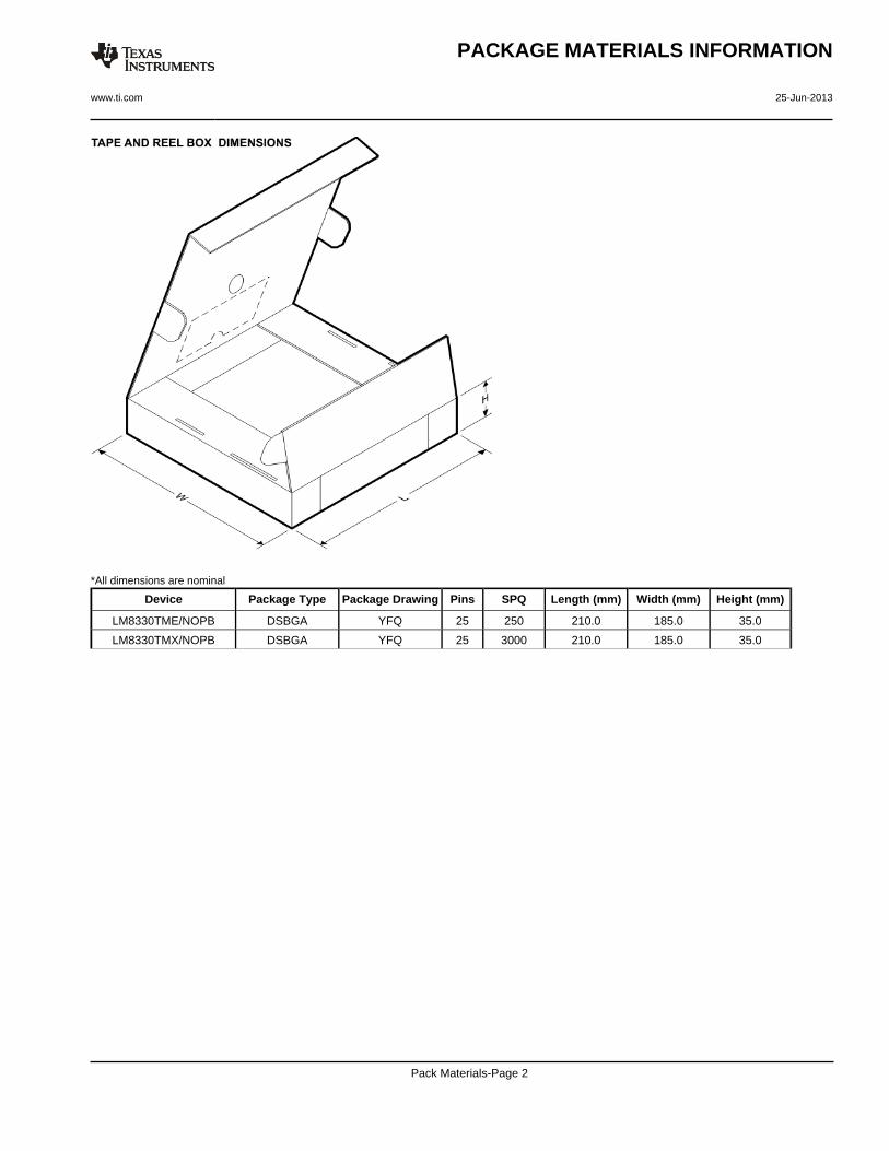
*All dimensions are nominal
Device Package Type Package Drawing Pins SPQ Length (mm) Width (mm) Height (mm)
LM8330TME/NOPB DSBGA YFQ 25 250 210.0 185.0 35.0
LM8330TMX/NOPB DSBGA YFQ 25 3000 210.0 185.0 35.0
PACKAGE MATERIALS INFORMATION
www.ti.com 25-Jun-2013
Pack Materials-Page 2
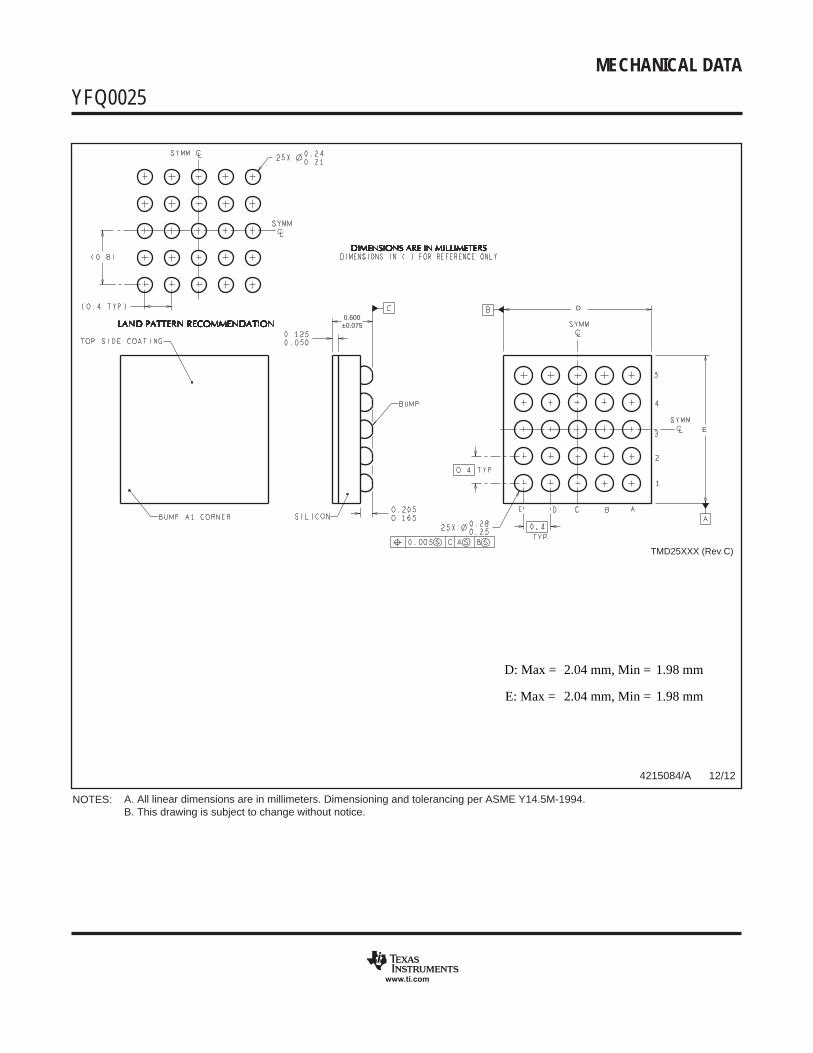
MECHANICAL DATA
YFQ0025xxx
www.ti.com
TMD25XXX (Rev C)
A. All linear dimensions are in millimeters. Dimensioning and tolerancing per ASME Y14.5M-1994.B. This drawing is subject to change without notice.
NOTES:
4215084/A 12/12
D0.600±0.075
E
D: Max =
E: Max =
2.04 mm, Min =
2.04 mm, Min =
1.98 mm
1.98 mm

IMPORTANT NOTICE
Texas Instruments Incorporated (TI) reserves the right to make corrections, enhancements, improvements and other changes to itssemiconductor products and services per JESD46, latest issue, and to discontinue any product or service per JESD48, latest issue. Buyersshould obtain the latest relevant information before placing orders and should verify that such information is current and complete.TI’s published terms of sale for semiconductor products (http://www.ti.com/sc/docs/stdterms.htm) apply to the sale of packaged integratedcircuit products that TI has qualified and released to market. Additional terms may apply to the use or sale of other types of TI products andservices.Reproduction of significant portions of TI information in TI data sheets is permissible only if reproduction is without alteration and isaccompanied by all associated warranties, conditions, limitations, and notices. TI is not responsible or liable for such reproduceddocumentation. Information of third parties may be subject to additional restrictions. Resale of TI products or services with statementsdifferent from or beyond the parameters stated by TI for that product or service voids all express and any implied warranties for theassociated TI product or service and is an unfair and deceptive business practice. TI is not responsible or liable for any such statements.Buyers and others who are developing systems that incorporate TI products (collectively, “Designers”) understand and agree that Designersremain responsible for using their independent analysis, evaluation and judgment in designing their applications and that Designers havefull and exclusive responsibility to assure the safety of Designers' applications and compliance of their applications (and of all TI productsused in or for Designers’ applications) with all applicable regulations, laws and other applicable requirements. Designer represents that, withrespect to their applications, Designer has all the necessary expertise to create and implement safeguards that (1) anticipate dangerousconsequences of failures, (2) monitor failures and their consequences, and (3) lessen the likelihood of failures that might cause harm andtake appropriate actions. Designer agrees that prior to using or distributing any applications that include TI products, Designer willthoroughly test such applications and the functionality of such TI products as used in such applications.TI’s provision of technical, application or other design advice, quality characterization, reliability data or other services or information,including, but not limited to, reference designs and materials relating to evaluation modules, (collectively, “TI Resources”) are intended toassist designers who are developing applications that incorporate TI products; by downloading, accessing or using TI Resources in anyway, Designer (individually or, if Designer is acting on behalf of a company, Designer’s company) agrees to use any particular TI Resourcesolely for this purpose and subject to the terms of this Notice.TI’s provision of TI Resources does not expand or otherwise alter TI’s applicable published warranties or warranty disclaimers for TIproducts, and no additional obligations or liabilities arise from TI providing such TI Resources. TI reserves the right to make corrections,enhancements, improvements and other changes to its TI Resources. TI has not conducted any testing other than that specificallydescribed in the published documentation for a particular TI Resource.Designer is authorized to use, copy and modify any individual TI Resource only in connection with the development of applications thatinclude the TI product(s) identified in such TI Resource. NO OTHER LICENSE, EXPRESS OR IMPLIED, BY ESTOPPEL OR OTHERWISETO ANY OTHER TI INTELLECTUAL PROPERTY RIGHT, AND NO LICENSE TO ANY TECHNOLOGY OR INTELLECTUAL PROPERTYRIGHT OF TI OR ANY THIRD PARTY IS GRANTED HEREIN, including but not limited to any patent right, copyright, mask work right, orother intellectual property right relating to any combination, machine, or process in which TI products or services are used. Informationregarding or referencing third-party products or services does not constitute a license to use such products or services, or a warranty orendorsement thereof. Use of TI Resources may require a license from a third party under the patents or other intellectual property of thethird party, or a license from TI under the patents or other intellectual property of TI.TI RESOURCES ARE PROVIDED “AS IS” AND WITH ALL FAULTS. TI DISCLAIMS ALL OTHER WARRANTIES ORREPRESENTATIONS, EXPRESS OR IMPLIED, REGARDING RESOURCES OR USE THEREOF, INCLUDING BUT NOT LIMITED TOACCURACY OR COMPLETENESS, TITLE, ANY EPIDEMIC FAILURE WARRANTY AND ANY IMPLIED WARRANTIES OFMERCHANTABILITY, FITNESS FOR A PARTICULAR PURPOSE, AND NON-INFRINGEMENT OF ANY THIRD PARTY INTELLECTUALPROPERTY RIGHTS. TI SHALL NOT BE LIABLE FOR AND SHALL NOT DEFEND OR INDEMNIFY DESIGNER AGAINST ANY CLAIM,INCLUDING BUT NOT LIMITED TO ANY INFRINGEMENT CLAIM THAT RELATES TO OR IS BASED ON ANY COMBINATION OFPRODUCTS EVEN IF DESCRIBED IN TI RESOURCES OR OTHERWISE. IN NO EVENT SHALL TI BE LIABLE FOR ANY ACTUAL,DIRECT, SPECIAL, COLLATERAL, INDIRECT, PUNITIVE, INCIDENTAL, CONSEQUENTIAL OR EXEMPLARY DAMAGES INCONNECTION WITH OR ARISING OUT OF TI RESOURCES OR USE THEREOF, AND REGARDLESS OF WHETHER TI HAS BEENADVISED OF THE POSSIBILITY OF SUCH DAMAGES.Unless TI has explicitly designated an individual product as meeting the requirements of a particular industry standard (e.g., ISO/TS 16949and ISO 26262), TI is not responsible for any failure to meet such industry standard requirements.Where TI specifically promotes products as facilitating functional safety or as compliant with industry functional safety standards, suchproducts are intended to help enable customers to design and create their own applications that meet applicable functional safety standardsand requirements. Using products in an application does not by itself establish any safety features in the application. Designers mustensure compliance with safety-related requirements and standards applicable to their applications. Designer may not use any TI products inlife-critical medical equipment unless authorized officers of the parties have executed a special contract specifically governing such use.Life-critical medical equipment is medical equipment where failure of such equipment would cause serious bodily injury or death (e.g., lifesupport, pacemakers, defibrillators, heart pumps, neurostimulators, and implantables). Such equipment includes, without limitation, allmedical devices identified by the U.S. Food and Drug Administration as Class III devices and equivalent classifications outside the U.S.TI may expressly designate certain products as completing a particular qualification (e.g., Q100, Military Grade, or Enhanced Product).Designers agree that it has the necessary expertise to select the product with the appropriate qualification designation for their applicationsand that proper product selection is at Designers’ own risk. Designers are solely responsible for compliance with all legal and regulatoryrequirements in connection with such selection.Designer will fully indemnify TI and its representatives against any damages, costs, losses, and/or liabilities arising out of Designer’s non-compliance with the terms and provisions of this Notice.
Mailing Address: Texas Instruments, Post Office Box 655303, Dallas, Texas 75265Copyright © 2017, Texas Instruments Incorporated