solns_13 cmos
TRANSCRIPT

Problem 13.1) Krishna Duvvada Estimate and simulate the delay through 10 TG’s connected a 50fF load capacitance. Use the 50nm short channel CMOS process with the parameters seen in Table 10.2. Solution:-
From Table 10.2, for short channel (50nm) process, Rn=Rp=3.4K ohms. Cox,n=0.645fF & Cox,p=1.25fF tPHL = tPLH = [0.35 * (Rn//Rp) * (Cox,n + Cox,p ) * 102 ] + [0.7 * 10 * (Rn//Rp) * 50fF]
= [0.35 * (1.7K) * (1.25+0.625 )fF * 102 ] + [0.7 * 10 * (1.7K) * 50fF] = (111.5625 + 595)ps = 706.562 ps
Spice net list:- ***Problem-(13.1) .control destroy all run plot vin N10 ylimit 0 1 .endc .option scale=50n .tran .05n 100n
td =0.7ns

vdd vdd 0 DC 1 Vin vin 0 DC 0 pulse 0 1 0 0 0 20n 40n X1 vin N1 TG X2 N1 N2 TG X3 N2 N3 TG X4 N3 N4 TG X5 N4 N5 TG X6 N5 N6 TG X7 N6 N7 TG X8 N7 N8 TG X9 N8 N9 TG X10 N9 N10 TG cl N10 0 50f .Subckt TG in out vdd vdd 0 DC 1 M1 in vdd out 0 NMOs L=1 w=10 M2 in 0 out vdd PMOS L=1 w=20 .ends
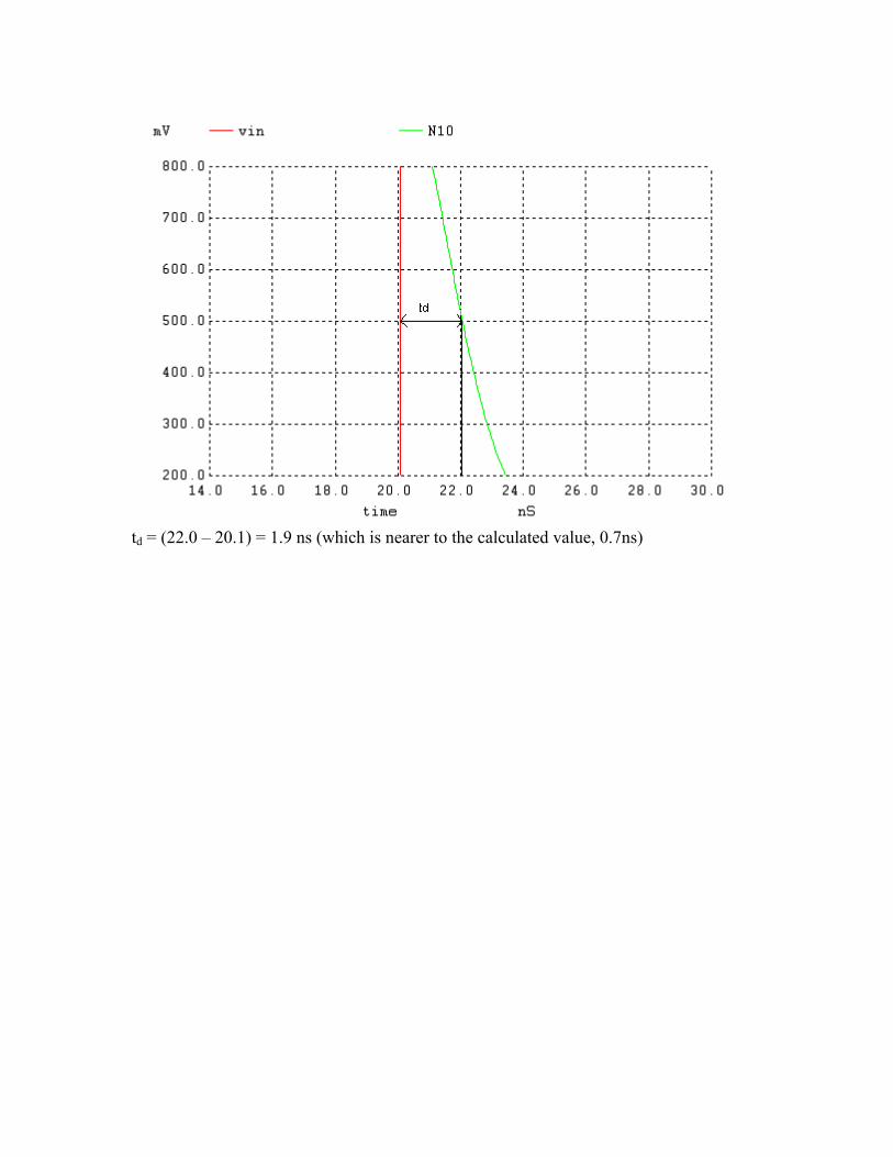
td = (22.0 – 20.1) = 1.9 ns (which is nearer to the calculated value, 0.7ns)

13.2) Surendranath C Eruvuru Design and simulate the operation of a half adder circuit using TGs. Following is the truth table of a Half Adder:
In the following circuit all the PMOS transistors are 20/1 and all NMOS transistors are 10/1 in measurements. Both the SUM logic and the CARRY logic have two transmission gates (TG) output capacitances to discharge through Rn // Rp resistance. So, THL + THL from hand calculations is 4.46ps.
Circuit for SUM
Circuit for Carry
Netlist: .CONTROL DESTROY ALL RUN plot A 1.25+B 2.5+S 3.75+C .ENDC .option scale=50n .tran .1n 10n UIC
A B Sum Carry 0 0 1 1
0 1 0 1
0 1 1 1
0 0 0 1

VA A 0 DC 0 PULSE 1 0 1n .01n .01n 2n 4n VAI AI 0 DC 0 PULSE 0 1 1n .01n .01n 2n 4n VB B 0 DC 0 PULSE 1 0 2n .01n .01n 2n 4n VBI BI 0 DC 0 PULSE 0 1 2n .01n .01n 2n 4n VDD VDD 0 DC 1 XTG1 B A AI S Vdd TG XTG2 BI AI A S Vdd TG XTG3 0 B BI C Vdd TG XTG4 A BI B C Vdd TG **************************SUBCKT 1******************************************************* .SUBCKT TG in1 in2 in3 out1 Vdd M1 out1 in2 in1 Vdd PMOS L=1 W=20 M2 out1 in3 in1 0 NMOS L=1 W=10 .ENDS Simulation result for Half Adder:
Delay measured from simulations: TLH = 20ps. THL = 19ps.

Problem 13.3 Satish Dulam Question: Sketch the schematic of an 8 to 1 DEMUX using NMOS PGs. Estimate the delay through the DEMUX when the output is connected to a 50fF load capacitance. Solution: The schematic of the DEMUS using NMOS PGs is shown below:
S3 S2 S1 Z 0 0 0 A 0 0 1 B 0 1 0 C 0 1 1 D 1 0 0 E 1 0 1 F 1 1 0 G 1 1 1 H
When all the select lines are low (S3, S2, S1) = (0, 0, 0), the Z value is propagated to the node A, and when the (S3, S2, S1) = (0, 0, 1), the Z value is propagated to the output node B and so on.

Spice Simulations showing that with the (S3, S2, S1) = (0, 0, 0) the output node A followed the node Z and when (S3, S2, S1) = (1, 0, 0) the output node e followed the node Z. *Prob 13.3 DEMUX .control destroy all run plot VZ Vs1+2 vs2+4 vs3+6 va+8 Vb+10 Vc+12 vd+14 ve+16 vf+18 vg+20 .endc .option scale=50n .tran 100p 24n UIC .IC V(va)=0 V(vb)=0 V(vc)=0 V(vd)=0 V(ve)=0 V(vf)=0 V(vg)=0 vdd vdd 0 DC 1 VZ VZ 0 DC 0 pulse 0 1 5n 0 0 5n 10n VSEL1 VSEL1 0 DC 0 pulse 0 1 14n 0 0 7n 14n VSEL2 VSEL2 0 DC 0 VSEL3 VSEL3 0 DC 0 XINV1 VSEL1 Vs1bar vdd 0 INV XINV2 Vs1bar Vs1 vdd 0 INV XINV3 VSEL2 Vs2bar vdd 0 INV XINV4 Vs2bar Vs2 vdd 0 INV XINV5 VSEL3 Vs3bar vdd 0 INV XINV6 Vs3bar Vs3 vdd 0 INV M1 Va Vs3bar temp1 0 NMOS L=1 W=10 M2 Vb Vs3 temp1 0 NMOS L=1 W=10 M3 Vc Vs3bar temp2 0 NMOS L=1 W=10 M4 Vd Vs3 temp2 0 NMOS L=1 W=10 M5 temp1 Vs2bar temp3 0 NMOS L=1 W=10 M6 temp2 Vs2 temp3 0 NMOS L=1 W=10 M7 temp3 Vs1bar VZ 0 NMOS L=1 W=10 M8 Ve Vs3bar temp4 0 NMOS L=1 W=10 M9 Vf Vs3 temp4 0 NMOS L=1 W=10 M10 Vg Vs3bar temp5 0 NMOS L=1 W=10 M11 Vh Vs3 temp5 0 NMOS L=1 W=10 M12 temp4 Vs2bar temp6 0 NMOS L=1 W=10 M13 temp5 Vs2 temp6 0 NMOS L=1 W=10 M14 temp6 Vs1 VZ 0 NMOS L=1 W=10 Cloada va 0 50f Cloadb vb 0 50f Cloadc vc 0 50f Cloadd vd 0 50f Cloade ve 0 50f Cloadf vf 0 50f Cloadg vg 0 50f Cloadh vh 0 50f .SUBCKT INV INV_in INV_out INV_Vdd INV_gnd Minv1 INV_out INV_in INV_vdd INV_vdd PMOS L=1 W=20 Minv2 INV_out INV_in INV_gnd INV_gnd NMOS L=1 W=10 .ENDS * 50nm BSIM4 models


Vinay Dindi 13.4) Verify, using SPICE, that the circuit seen in Fig. 13.12 operates as an XOR gate.
The circuit is simulated in winspice with PMOS and NMOS sizes as 20/1 and 10/1 respectively. Netlist is as shown below..

Truth table of an XOR gate A B Out 0 0 0 0 1 1 1 0 1 1 1 0 Note: In the netlist A=Vin1, Abar=Vin1bar, B=Vin2, Bbar=Vin2bar. The output of the simulation is as shown below

Problem 13.5 :- Simulate the operation of an SR latch made with NAND gates. Show all four possible combinations. Solution:- *netlist for the circuit .control destroy all run plot vr vS+1.5 vQ+3 vq1+4.5 VQ1+4.5 ylimit 0 6 .endc .option scale=50n .tran .01n 4n vS vS 0 DC 0 pulse(0 1 1n 0 0 1n 2n) vR vR 0 DC 0 pulse(0 1 2n 0 0 2n 4n)

Rahul Mhatre 13.6 Simulate the operation of the Arbiter seen in Fig. 13.15. Show how two inputs arriving at the same time results in only one output going high.
Figure 13.15 An arbiter made using NAND gates. Solution The input stage is a SR NAND latch as seen in the figure below. The output of the
NAND latch powers the inverters. Truth Table S R Q Qbar 0 0 1 1 0 1 1 0 1 0 0 1 1 1 Q Qbar
Figure 13.6.1 Set-reset NAND latch.
Out1
Out2
M4 20/1
M1 10/1
M2 20/1
M3 10/1
In1
In2
20/20
20/20
Q
Qbar
S
R Q
20/20
Qbar

The truth table for the NAND latch is shown in Figure 13.6.1. So if S (In 1) is high, Q is low. As a result Out 1 is high, because it has a low input and is powered by Q. This can be seen in the simulation results of Figure 13.6.2. Out 2 is low because of the similar reason. Similarly if R is high, Qbar is low, and Out2 is high and Out1 is low. When both the arbiter inputs go low, both the arbiter outputs are also low. This is also observed in the simulations of Figure 1.6.2.
If, the arbiter is in steady state (one output high and the other low), and both the inputs are high, the arbiter maintains its steady state because of the latch action of the NAND latch (Q and Qbar maintain their states if both the inputs are high, as seen in the Truth table). This is seen in the simulation Figure 13.6.2. The simulation shows the outputs Out1 and Out2 for all combinations of inputs Vin1 and Vin2 (namely 00, 01, 10 and 11). Consider a scenario that during the initial power up, both the inputs go high at the same time. Because of the propagation delay mismatch in the feedback paths of the NAND gates in the latch, (delays depend upon layout), either Q or Qbar, but not both, goes high. Accordingly, either Out1 or Out2 will be high. This is also observed in the simulation of Figure 13.6.2. Thus, the circuit act as an arbiter for the two inputs. The spice simulation file is as given below. *** Problem 12.6 CMOS: Circuit Design, Layout, and Simulation *** .control destroy all run plot vin1 vin2+1.25 out1+2.5 out2+3.75

.endc .option scale=1u .tran 10n 450n 0n UIC vdd vdd 0 DC 1 vin1 vin1 0 DC 0 PWL(0 0 49n 0 50n 1 99n 1 100n 0 149n 0 150n 1 199n 1 200n 0 349n 0 350n 1) vin2 vin2 0 DC 0 PWL(0 0 49n 0 50n 1 99n 1 100n 0 249n 0 250n 1 299n 1 300n 0 349n 0 350n 1) x1 vin1 n2 n1 vdd NAND_2 x2 n1 vin2 n2 vdd NAND_2 x3 n1 n2 out1 vdd INV X4 n2 n1 out2 vdd INV cout1 out1 0 5f IC=0 cout2 out2 0 5f IC=0 .subckt NAND_2 A B out VDD M1 n1 A 0 0 NMOS L=1 W=20 M2 out B n1 0 NMOS L=1 W=20 M3 out A VDD VDD PMOS L=1 W=20 M4 out B VDD VDD PMOS L=1 W=20 .ends .subckt INV A B OUT VDD M5 OUT A 0 0 NMOS L=1 W=20 M6 OUT A B VDD PMOS L=1 W=10 .ends * 1 um Level 3 models * * Don't forget the .options scale=1u if using an Lmin of 1 * 1<Ldrawn<200 10<Wdrawn<10000 Vdd=5V * Long Channel NMOS and PMOS models .end

Problem 13.7 Indira Show using simulations, how making the feedback inverter in Fig. 13.18 stronger (decreasing the lengths) can result in the output having either a long delay or not fully switching? Solution:
****problem 13.7***** .control detroy all run plot VQ VIN+1.5 VCLK+3 .endc .option scale=50n .tran 10p 10n 10P UIC VDD VDD 0 DC 1 VIN VIN 0 DC 0 PULSE 0 1 1.6N 0 0 1N 2N VCLK VCLK 0 DC 0 PULSE 0 1 2N 0 0 2N 4N M1 VOUT1 VCLK VIN 0 NMOS L=1 W=10 M2 VQ1 VOUT1 0 0 NMOS L=1 W=10 M3 VQ1 VOUT1 VDD VDD PMOS L=1 W=20 M4 VOUT1 VQ1 0 0 NMOS L=10 W=10 M5 VOUT1 VQ1 VDD VDD PMOS L=10 W=10 M6 VQ VQ1 0 0 NMOS L=1 W=10 M7 VQ VQ1 VDD VDD PMOS L=1 W=20

Using L=10 for the inverter 12 will give an output which is fully switching as shown in the above simulation. ****problem 13.7***** .control detroy all run plot VQ VIN+1.5 VCLK+3 .endc .option scale=50n .tran 10p 10n 10P UIC VDD VDD 0 DC 1 VIN VIN 0 DC 0 PULSE 0 1 1.6N 0 0 1N 2N VCLK VCLK 0 DC 0 PULSE 0 1 2N 0 0 2N 4N M1 VOUT1 VCLK VIN 0 NMOS L=1 W=10 M2 VQ1 VOUT1 0 0 NMOS L=1 W=10 M3 VQ1 VOUT1 VDD VDD PMOS L=1 W=20 M4 VOUT1 VQ1 0 0 NMOS L=5 W=10 M5 VOUT1 VQ1 VDD VDD PMOS L=5 W=10 M6 VQ VQ1 0 0 NMOS L=1 W=10 M7 VQ VQ1 VDD VDD PMOS L=1 W=20
Using L=5 for the inverter 12 will result in an output which is not switching completely as shown in the above simulation. Therefore decreasing the length of the feedback inverter 12 will cause the output not to switch fully or either an output having longer delay.
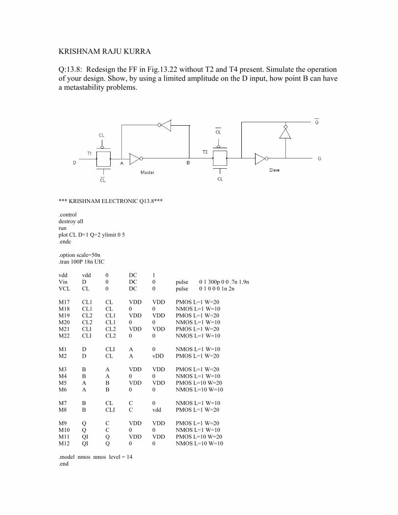
KRISHNAM RAJU KURRA Q:13.8: Redesign the FF in Fig.13.22 without T2 and T4 present. Simulate the operation of your design. Show, by using a limited amplitude on the D input, how point B can have a metastability problems.
*** KRISHNAM ELECTRONIC Q13.8*** .control destroy all run plot CL D+1 Q+2 ylimit 0 5 .endc .option scale=50n .tran 100P 18n UIC vdd vdd 0 DC 1 Vin D 0 DC 0 pulse 0 1 300p 0 0 .7n 1.9n VCL CL 0 DC 0 pulse 0 1 0 0 0 1n 2n M17 CL1 CL VDD VDD PMOS L=1 W=20 M18 CL1 CL 0 0 NMOS L=1 W=10 M19 CL2 CL1 VDD VDD PMOS L=1 W=20 M20 CL2 CL1 0 0 NMOS L=1 W=10 M21 CLI CL2 VDD VDD PMOS L=1 W=20 M22 CLI CL2 0 0 NMOS L=1 W=10 M1 D CLI A 0 NMOS L=1 W=10 M2 D CL A vDD PMOS L=1 W=20 M3 B A VDD VDD PMOS L=1 W=20 M4 B A 0 0 NMOS L=1 W=10 M5 A B VDD VDD PMOS L=10 W=20 M6 A B 0 0 NMOS L=10 W=10 M7 B CL C 0 NMOS L=1 W=10 M8 B CLI C vdd PMOS L=1 W=20 M9 Q C VDD VDD PMOS L=1 W=20 M10 Q C 0 0 NMOS L=1 W=10 M11 QI Q VDD VDD PMOS L=10 W=20 M12 QI Q 0 0 NMOS L=10 W=10 .model nmos nmos level = 14 .end
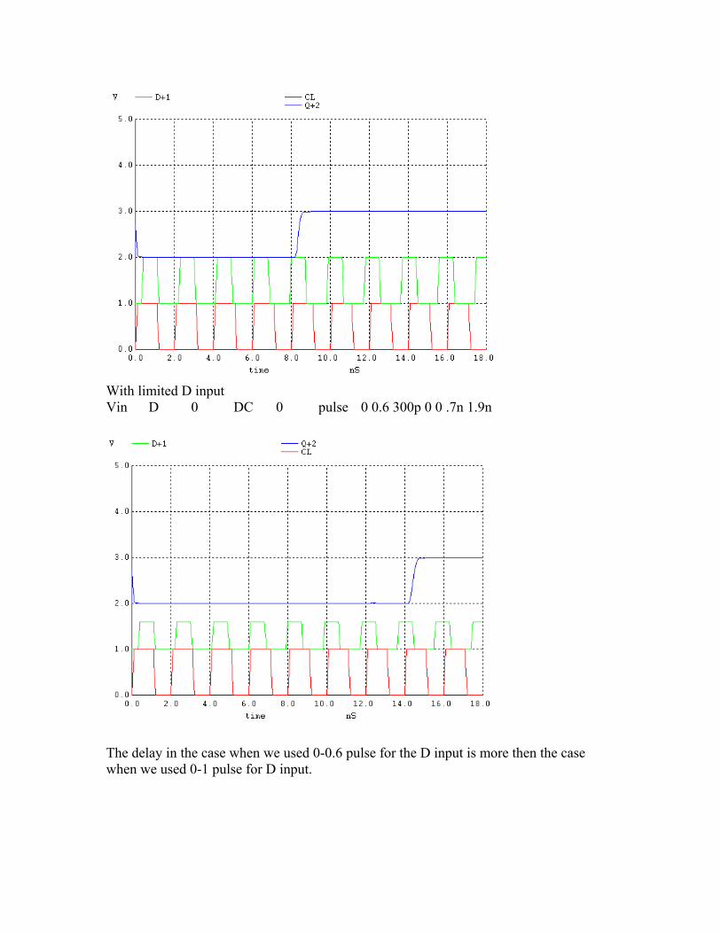
With limited D input Vin D 0 DC 0 pulse 0 0.6 300p 0 0 .7n 1.9n
The delay in the case when we used 0-0.6 pulse for the D input is more then the case when we used 0-1 pulse for D input.
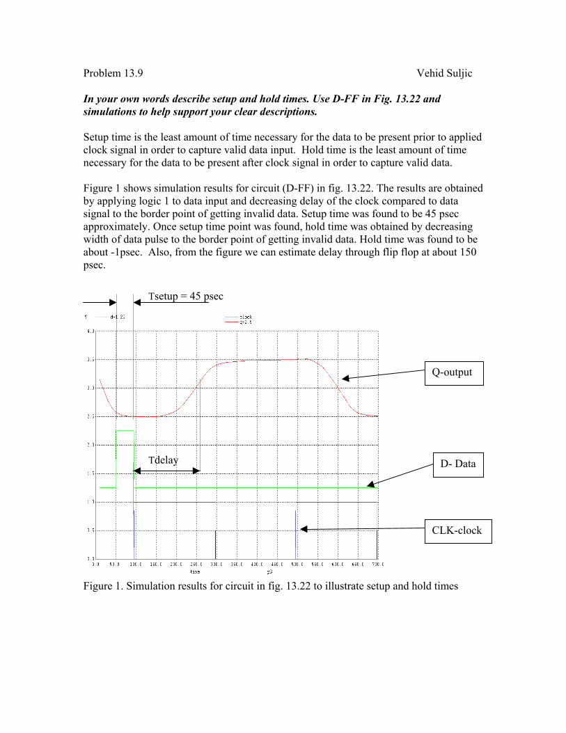
Problem 13.9 Vehid Suljic In your own words describe setup and hold times. Use D-FF in Fig. 13.22 and simulations to help support your clear descriptions. Setup time is the least amount of time necessary for the data to be present prior to applied clock signal in order to capture valid data input. Hold time is the least amount of time necessary for the data to be present after clock signal in order to capture valid data. Figure 1 shows simulation results for circuit (D-FF) in fig. 13.22. The results are obtained by applying logic 1 to data input and decreasing delay of the clock compared to data signal to the border point of getting invalid data. Setup time was found to be 45 psec approximately. Once setup time point was found, hold time was obtained by decreasing width of data pulse to the border point of getting invalid data. Hold time was found to be about -1psec. Also, from the figure we can estimate delay through flip flop at about 150 psec.
Figure 1. Simulation results for circuit in fig. 13.22 to illustrate setup and hold times
Q-output
CLK-clock
D- Data
Tsetup = 45 psec
Tdelay
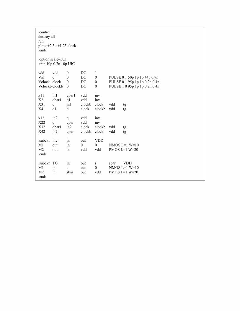
.control destroy all run plot q+2.5 d+1.25 clock .endc .option scale=50n .tran 10p 0.7n 10p UIC vdd vdd 0 DC 1 Vin d 0 DC 0 PULSE 0 1 50p 1p 1p 44p 0.7n Vclock clock 0 DC 0 PULSE 0 1 95p 1p 1p 0.2n 0.4n Vclockb clockb 0 DC 0 PULSE 1 0 95p 1p 1p 0.2n 0.4n x11 in1 qbar1 vdd inv X21 qbar1 q1 vdd inv X31 d in1 clockb clock vdd tg X41 q1 d clock clockb vdd tg x12 in2 q vdd inv X22 q qbar vdd inv X32 qbar1 in2 clock clockb vdd tg X42 in2 qbar clockb clock vdd tg .subckt inv in out VDD M1 out in 0 0 NMOS L=1 W=10 M2 out in vdd vdd PMOS L=1 W=20 .ends .subckt TG in out s sbar VDD M1 in s out 0 NMOS L=1 W=10 M2 in sbar out vdd PMOS L=1 W=20 .ends