solution for electronics devices and circuits · (b) draw the hybrid equivalent model of voltage...
TRANSCRIPT
Mumbai University Electrical (Semester -III)
1 |www.brainheaters.in
Solution for Electronics Devices
and Circuits
May 2016
Index
Q.1)
a) …………………………………………………………………………. 2-3
b) …………………………………………………………………………. 4
c) …………………………………………………………………………. 5
d) …………………………………………………………………………. 5-6
Q.2)
a) …………………………………………………………………………. 7
b) …………………………………………………………………………. 8-10
Q.3)
a) …………………………………………………………………………. 11-17
b) …………………………………………………………………………. N.A
Q.4)
a) …………………………………………………………………………. N.A
b) …………………………………………………………………………. 18-19
Q.5)
a) …………………………………………………………………………. 20-24
b) …………………………………………………………………………. N.A
Q.6)
a) …………………………………………………………………………. 25-28
b) …………………………………………………………………………. 29-31

Mumbai University Electrical (Semester -III)
2 |www.brainheaters.in
Q.1)
A) Draw the block diagram of a DC power supply and explain the terms.
a) rectification efficiency b) Ripple factor (RF) c) PIV (05)
Ans :- Block Diagram of DC Power Supply
a)

Mumbai University Electrical (Semester -III)
3 |www.brainheaters.in

Mumbai University Electrical (Semester -III)
4 |www.brainheaters.in
c)
..

Mumbai University Electrical (Semester -III)
5 |www.brainheaters.in
B) State the advantage of negative feedback. (05)
Ans:- Negative Feedback
Advantage of Negative Feedback :-
Disadvantage of Negative Feedback :-
Application of Negative Feedback :-

Mumbai University Electrical (Semester -III)
6 |www.brainheaters.in
C) Compare RC and LC oscillators. (05)
Ans:-
Sr. no. RC oscillators LC oscillators
D) Explain with V-I characteristics the working principle of a schottky diode.
(05)
Ans:-V-I Characteristic :-

Mumbai University Electrical (Semester -III)
7 |www.brainheaters.in
Mumbai University Electrical (Semester -III)
8 |www.brainheaters.in
Q.2)
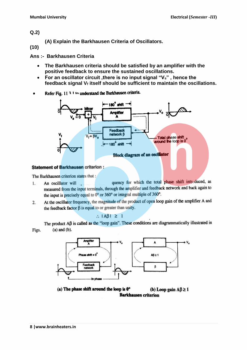
(A) Explain the Barkhausen Criteria of Oscillators. (10)
Ans :- Barkhausen Criteria
The Barkhausen criteria should be satisfied by an amplifier with the positive feedback to ensure the sustained oscillations.
For an oscillator circuit ,there is no input signal “Vs” , hence the feedback signal Vf itself should be sufficient to maintain the oscillations.
The
Mumbai University Electrical (Semester -III)
9 |www.brainheaters.in
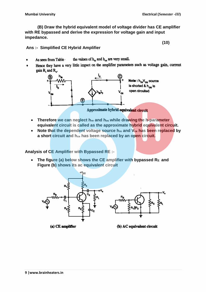
(B) Draw the hybrid equivalent model of voltage divider has CE amplifier
with RE bypassed and derive the expression for voltage gain and input
impedance.
(10)
Ans :- Simplified CE Hybrid Amplifier
Therefore we can neglect hre and hoc while drawing the h-parameter
equivalent circuit is called as the approximate hybrid equivalent circuit.
Note that the dependent voltage source hre and Vce has been replaced by
a short circuit and hce has been replaced by an open circuit.
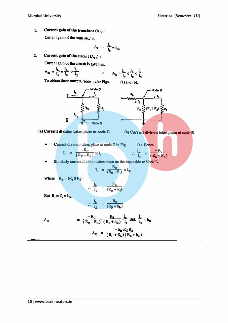
Analysis of CE Amplifier with Bypassed RE :-
The figure (a) below shows the CE amplifier with bypassed RE and
Figure (b) shows its ac equivalent circuit
Mumbai University Electrical (Semester -III)
10 |www.brainheaters.in

Mumbai University Electrical (Semester -III)
11 |www.brainheaters.in

Mumbai University Electrical (Semester -III)
12 |www.brainheaters.in
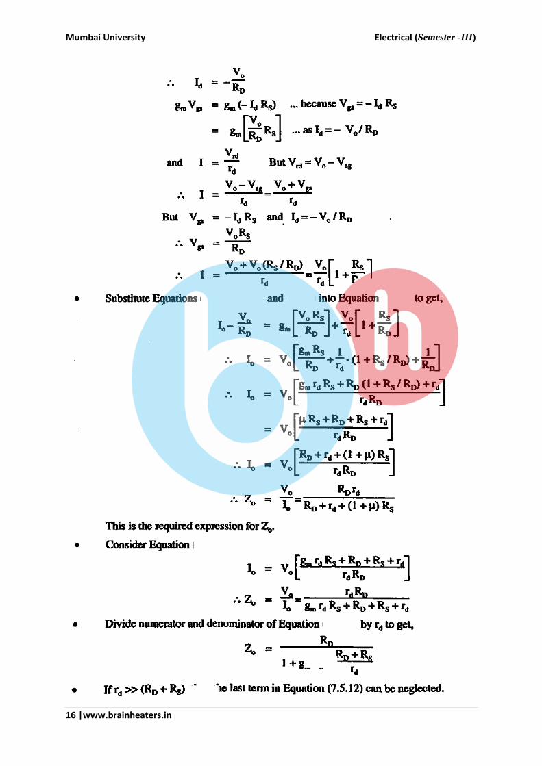
Q.3)
A) Draw the small signal equivalent of n-channel JFET amplifier with Rs
bypassed and un bypassed derive the expression for voltage gain in each
case. (10)
Ans :- JFET Amplifier
Analysis:
Let us obtain the expression for Z1 Z0 and Av for the self bias
configuration .
Compare the small signal equivalent circuit drawn in figure with the
small signal equivalent circuit of the fixed bias configuration.

Mumbai University Electrical (Semester -III)
13 |www.brainheaters.in
Ex. Of n-channel JFET :-

Mumbai University Electrical (Semester -III)
14 |www.brainheaters.in
CS JFET Amplifier with self Bias (Unbypassed Rs )

Mumbai University Electrical (Semester -III)
15 |www.brainheaters.in
Mumbai University Electrical (Semester -III)
16 |www.brainheaters.in

Mumbai University Electrical (Semester -III)
17 |www.brainheaters.in

Mumbai University Electrical (Semester -III)
18 |www.brainheaters.in
B) Find the voltage gain of a two stage caseadad JFET amplifier with the
following parameters.
VDD = 20V , RG1 = RG2 = 3.3 Ω , RD1 = RD2 = 2.4 Ω , RS1 = RS2 = 680 Ω IDSS = 10
mA , Vp = -4V (10)
Ans :- N. A.
Q.4)
A) Explain the different thermal compensation techniques in BJT amplifier. (10)
Ans :- N. A.

Mumbai University Electrical (Semester -III)
19 |www.brainheaters.in
B) State and draw each topology of negative feedback and explain the effect
on i/p impedance, o/p impedance and voltage gain for Current Series Negative
Feedback. (10)
Ans :- Negative feedback
Voltage series feedback :-

Mumbai University Electrical (Semester -III)
20 |www.brainheaters.in
Voltage shunt feedback :-
Current Shunt feedback :-
Mumbai University Electrical (Semester -III)
21 |www.brainheaters.in
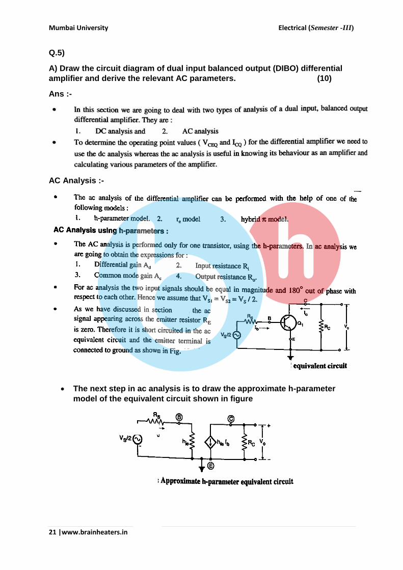
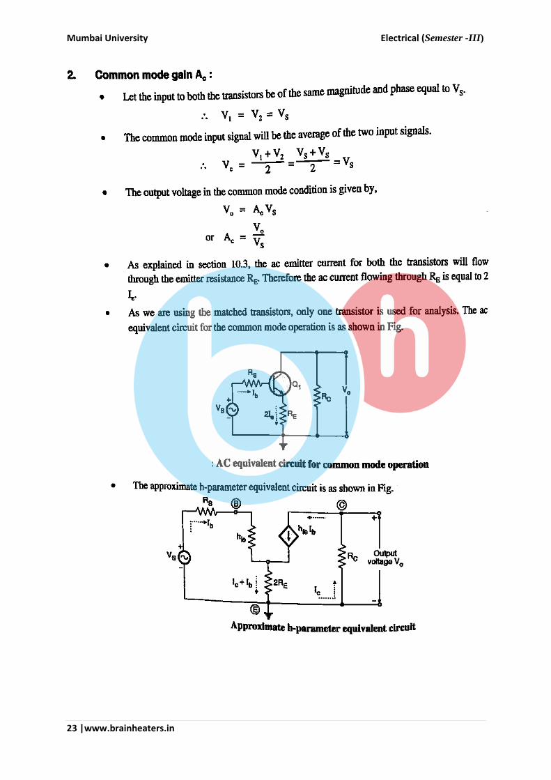
Q.5)
A) Draw the circuit diagram of dual input balanced output (DIBO) differential
amplifier and derive the relevant AC parameters. (10)
Ans :-
AC Analysis :-
The next step in ac analysis is to draw the approximate h-parameter
model of the equivalent circuit shown in figure
Mumbai University Electrical (Semester -III)
22 |www.brainheaters.in
Mumbai University Electrical (Semester -III)
23 |www.brainheaters.in

Mumbai University Electrical (Semester -III)
24 |www.brainheaters.in

Mumbai University Electrical (Semester -III)
25 |www.brainheaters.in
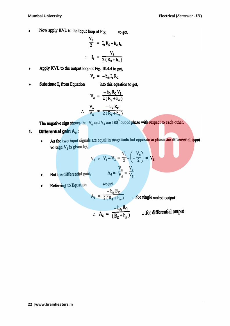
The expression for their voltage gain Ad , input resistance Rin and output
resistance R0 are as listed in table.
B) Derive the equation for frequency of oscillation of RC phase shift oscillators
using JFET as basic amplifier Derive the condition of Oscillation. (10)
Ans :- N.A
v
Mumbai University Electrical (Semester -III)
26 |www.brainheaters.in
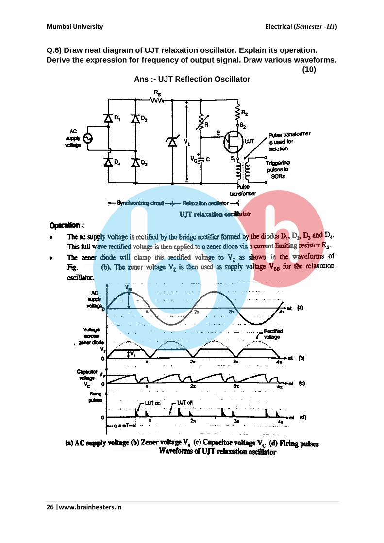
Q.6) Draw neat diagram of UJT relaxation oscillator. Explain its operation.
Derive the expression for frequency of output signal. Draw various waveforms.
(10)
Ans :- UJT Reflection Oscillator

Mumbai University Electrical (Semester -III)
27 |www.brainheaters.in
The capacitor charges through the potentiometer R. When the capacitor
voltage equals the peak voltage Vp of the UJT ,it turns on.
Then the capacitor discharges through emitter (E) ,base (B1) and primary
winding of the pulse transformer .
Due to primary current, a pulse is generated on the secondary side of
the pulse transformer.
The capacitor voltage and secondary pulses are as shown in the figures
respectively.
These pulses are used as triggering pulses for the SCR.
As the capacitor discharges and Vc reaches the point voltage VV ,the UJT
is turned off and the capacitor starts charging again through R.
The charging rate of the capacitor is decided by the value R .Therefore it
is possible to change the firing angle α by varying the potentiometer
R.the firing angle can be changed from 0 to 180 0.
c

Mumbai University Electrical (Semester -III)
28 |www.brainheaters.in

Mumbai University Electrical (Semester -III)
29 |www.brainheaters.in

Mumbai University Electrical (Semester -III)
30 |www.brainheaters.in
B) What is Darlington configuration? Derive the expression of voltage gain of
Darlington pair emitter follower. (10)
Ans :- Darlington Pair
1) Emitter Follower using Darlington pair :-

Mumbai University Electrical (Semester -III)
31 |www.brainheaters.in
2) Analysis of Darlington Emitter Follower :-
Voltage gains of Darlington Connection :-
The overall voltage gain Av is given by,
So let us obtain the expression for the individual voltage gains Av1 and
Av2.
Voltage gain for second stage Is obtained by using approximate
analysis and Av1 is obtained by using the exact analysis.

Mumbai University Electrical (Semester -III)
32 |www.brainheaters.in