solution-processed in2s3 buffer layer for chalcopyrite ... · pdf fileby adjusting the ink ......
TRANSCRIPT

EPJ Photovoltaics 7, 70303 (2016)www.epj-pv.orgDOI: 10.1051/epjpv/2016001
EPJ PhotovoltaicsEPJ Photovoltaics
Open Access
Solution-processed In2S3 buffer layer for chalcopyrite thin filmsolar cells
Lan Wang1,a, Xianzhong Lin1, Ahmed Ennaoui2, Christian Wolf1, Martha Ch. Lux-Steiner1,3, and Reiner Klenk1
1 Helmholtz-Zentrum Berlin fur Materialien und Energie, Hahn-Meitner-Platz 1, 14109 Berlin, Germany2 Qatar Environment and Energy Research Institute and Hamad Bin Khalifa University, Education City, Doha, Qatar3 Freie Universitat Berlin, Fachbereich Physik, Arnimallee 14, 14195 Berlin, Germany
Received: 4 December 2015 / Received in final form: 22 January 2016/ Accepted: 27 January 2016Published online: 26 February 2016c© Wang et al., published by EDP Sciences, 2016
Abstract We report a route to deposit In2S3 thin films from air-stable, low-cost molecular precursor inksfor Cd-free buffer layers in chalcopyrite-based thin film solar cells. Different precursor compositions andprocessing conditions were studied to define a reproducible and robust process. By adjusting the inkproperties, this method can be applied in different printing and coating techniques. Here we report ontwo techniques, namely spin-coating and inkjet printing. Active area efficiencies of 12.8% and 12.2% havebeen achieved for In2S3-buffered solar cells respectively, matching the performance of CdS-buffered cellsprepared with the same batch of absorbers.
1 Introduction
While the industrial production of chalcopyrite solarmodules relies on vacuum-based deposition for most ofthe layers, there are in addition efforts to implement al-ternative vacuum-free methods. Among them, printingtechnologies are deemed attractive because of superiorutilization of raw materials and the potential for highthroughput roll-to-roll fabrication. Developments in thisarea have been concentrating mainly on the chalcopyriteabsorber [1,2]. The buffer layer, either CdS or, preferably,a Cd-free material such as Zn(O,S) [3, 4] or In2S3 [5–10],can be prepared by dry as well as solution-based processes.The latter are typically implemented by chemical bath de-position and could be combined with a printed absorberto implement vacuum-free manufacturing of the core com-ponents of the cell. Nevertheless, printing the buffer layercould offer additional advantages in terms of material us-age, in-line integration and with respect to the amountof (liquid) waste generated. In addition, certain printingtechnologies (such as inkjet printing [11]) provide highlylocalized deposition, direct patterning (without lithogra-phy) of materials in atmospheric environment and ex-cellent raw material utilization. This is very attractivefor the implementation of advanced cell concepts such asmicro-concentrator cells [12].
In this work, precursor inks (molecular inks) were de-veloped and combined with drying and annealing steps forthe fabrication of In2S3 buffers. By tuning the rheological
a e-mail: [email protected]
properties of the inks, both, spin-coating as well as inkjetprinting could be implemented. By optimizing the compo-sition of the precursor ink as well as the processing condi-tions, cells with more than 12% active area efficiency wereachieved for both process variants.
2 Experimental
The precursor-based processing of indium sulphidethin films consists of four steps (see Fig. 1): (i) formu-lation of metal salt precursor inks, (ii) spin coating/inkjetprinting, (iii) pre-heating of deposited inks and (iv) an-nealing in H2S/Ar atmosphere. Firstly, a precursor ink wasformulated by adding 1 mmol In(NO3)3 (Sigma-Aldrich,99.99%) and 1.5 mmol thiourea (SC(NH2)2, Merck, 99%)to an ethanol-based solvent (containing 9 mL ethanoland 1 mL ethylene glycol). Assuming that each thioureamolecule results in one free sulphur atom, the In/S ra-tio was then in nominal accordance with the stoichiome-try of the In2S3 compound. However, different ratios wereused in the experiments to study the influence on the cellperformance. The ink was subjected to continuous stir-ring until it became transparent. Secondly, the precursorink was deposited by either spin coating or inkjet print-ing onto substrates. For inkjet printing, a PiXDRO LP50inkjet printer (Roth & Rau B.V.) and an industrial-gradeTrident 256JetTM printhead (Trident, ITW) were used.The Trident print head has 256 piezoelectric nozzles, eachwith a diameter of 50 μm and a nominal drop volume
This is an Open Access article distributed under the terms of the Creative Commons Attribution License (http://creativecommons.org/licenses/by/4.0),
which permits unrestricted use, distribution, and reproduction in any medium, provided the original work is properly cited.

2 L. Wang et al.: EPJ Photovoltaics 7, 70303 (2016)
Fig. 1. Schematic diagram of In2S3 thin film formation process.
of 15−20 pL. The applied voltage and pulse duration ofeach nozzle can be tuned to obtain a well-jetted string ofdroplets. By increasing the resolution (dots per inch, dpi)of the printed pattern, deposited droplets can merge intoa continuous film. The resolution used in our experimentwas 500 dpi, in both X and Y directions. Then the samplewas pre-heated in air at 150 ◦C for 1 min to evaporate thesolvents and dry the film. Finally the pre-heated dry filmwas annealed in a quartz-tube furnace at 225 ◦C for 10 minunder 5% H2S in Ar atmosphere to drive the formation ofan In2S3 thin film. The quartz tube was evacuated andfilled with argon three times before starting annealing.
The structure of In2S3 thin films deposited onto glasssubstrates was characterized by X-ray diffraction (XRD)operated in a 2θ range of 10−70◦ on a Bruker D8-AdvanceX-ray diffractometer with Cu Kα1 radiation at an inci-dent angle of 0.5◦ (grazing incidence mode), using a stepsize of 0.02◦ and step time of 5 s. The thickness and mor-phology of buffer layers were analyzed in a LEO 1530GEMINI scanning electron microscope (SEM) of Zeiss.The SEM images were recorded at an acceleration voltageof 10 kV.
Test solar cells were fabricated by depositing the In2S3
buffers onto soda lime glass/Mo/absorber thin film stacks(cut down to a sample size of 2.5 × 2.5 cm2) from ourin-house large-area baseline. The sequential processingof Cu(In,Ga)Se2 absorbers relies on the chalcogenizationof a multi-layered sputtered metal CuGa/In precursor,which is performed in nitrogen at atmospheric pressureusing elemental Se [13]. Reference cells with chemicalbath deposited CdS buffers were made with absorbersfrom the same batch. All devices were completed withan i-ZnO/ZnO:Al window layer and Ni/Al grids. Mechan-ical scribing was applied on each sample to define 8 solarcells with an area of 0.5 cm2. Solar cells were measuredunder simulated AM 1.5 illumination and standard condi-tions. The cells were not annealed or light-soaked beforethe measurements. The quantum efficiency was recordedusing Xe arc and halogen lamps and a monochromator andreferenced to calibrated Si and Ge solar cells. The short-circuit current densities measured with the sun simulatorwere slightly too high due to spectral mismatch. Unlessstated otherwise, the values given below were calculatedfrom the measured quantum efficiency (EQE) measure-ment using a tabulated AM 1.5 reference spectrum andrefer to the active area of the devices [14].
Fig. 2. XRD patterns of indium sulfide films prepared fromprecursor inks drop-cast onto glass substrates, (a) thiourea-containing precursor annealed in air, (b) thiourea-freeprecursor annealed in H2S and (c) thiourea-containing precur-sor annealed in H2S. The annealing time was 30 min for allsamples.
3 Results
To confirm that the formation of In2S3 is possible inprinciple, precursor ink was drop-cast onto rinsed glasssubstrates followed by a pre-heating step in air at 150 ◦Cfor 1 min to remove residual solvents. XRD patterns ofthis pre-heated film showed no peak and further anneal-ing in air for 30 min led to broad peaks with low in-tensity (see Fig. 2a). Instead, when sulfurized in Ar/H2Sat 225 ◦C for 30 min, the film showed pronounced XRDpeaks (Fig. 2c) corresponding to β-In2S3(JCPDS 00-025-0390) phases, which indicates the formation of crystallinefilm at this moderate annealing temperature. To identifythe influence of thiourea, as a sulphur source, on the for-mation of In2S3, precursor ink without thiourea was alsoused for structural characterization. However, the XRDpattern of the obtained film shown in Figure 2b indicatesinferior crystallinity. Compared to Figure 2c, the intensi-ties of (311) and (400) reflections were decreased and em-bedded in a background presumably stemming from anamorphous phase.
By adjusting the spin coating parameters, a bufferlayer with a thickness of ca. 30 nm (after annealing) could

L. Wang et al.: EPJ Photovoltaics 7, 70303 (2016) 3
Fig. 3. SEM images of spin-coated films on glass/Mo substrates: (a) precursor film after pre-heating and (b) after annealing.
Table 1. Device parameters (best cells) of CIGSe solar cellswith standard CdS buffer, spin-coated (C-03, C-04, C-05 andC-06) and inkjet-printed (C-72, C-77) In2S3 buffers. SampleC-03 was prepared from the thiourea-free precursor, whileC-04, C-05 and C-06 were spin-coated from precursors withvaried In-S ratio 1:1, 1:2 and 1:3 respectively. C-72 was pre-pared with the buffer annealed only in argon atmosphere(without H2S), while C-77 was annealed in H2S-containingatmosphere.
Sample In/S Voc Jsc FF η
ratio (mV) (mA/cm2) (%) (%)
CdS − 511 39.1 63 12.5
C-03 − 389 39.6 49 7.6
C-04 1:1 478 39.9 55 10.4
C-05 1:2 491 39.2 66 12.8
C-06 1:3 485 38.6 61 11.5
C-72 1:2 458 37.5 63 10.8
C-77 1:2 481 38.6 65 12.2
be achieved. The cross-sections of spin-coated films on aglass/Mo substrate before and after annealing are shownin Figure 3. The thickness of the film after annealing wasslightly reduced (from 34 nm to 28 nm in the given SEMimages). Inkjet-printed films were similar in morphologyon a microscopic level but slightly thinner (25 nm beforeand 20 nm after annealing, respectively). In terms of mate-rial utilization, this drop-on-demand technique is superiorto spin coating. For instance, only 4 μL ink is needed toinkjet print a buffer layer on a standardized sample, incomparison with 100 μL ink required for spin coating.
Photovoltaic parameters of solar cells from a typicaltest run (best cells) are summarized in Table 1. To achievethe optimal solar cell efficiency, variations of the In/S ratio(1:1, 1:2 and 1:3) in the precursor were applied. The high-est efficiency (12.8%) was obtained with the In/S ratio of1:2 (C-05). The sample fabricated from the thiourea-freeprecursor (C-03) showed lower open-circuit voltage andfill factor compared to samples produced with thiourea-containing precursors. The transfer of the processing routefrom spin-coating to inkjet printing was successfully im-plemented, with the best cell efficiency of 12.2% (C-77).
Fig. 4. Average (16 cells) and best efficiencies of solar cellsbuffered with CdS, spin-coated In2S3 and inkjet-printed In2S3.The error bars represent the standard deviation.
Solar cells with a buffer annealed in pure argon (C-72)showed only slightly lower efficiency. For each experimen-tal condition, two 2.5 × 2.5 cm2 samples have been pre-pared identically, each containing 8 cells. The average andbest efficiencies of the cells are depicted in Figure 4. Thetrend of the average of cell efficiencies upon different pro-cessing conditions corresponds well with the best valuesand all the data are within a reasonable deviation range.
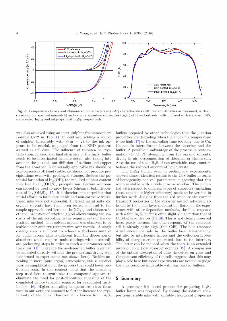
The current-voltage (J-V ) characteristics and externalquantum efficiencies (EQE) of selected best cells from Ta-ble 1 are presented in Figure 5. The J-V curves of bothcells with solution-processed In2S3 demonstrate diodeproperties (shunt and series resistance, diode quality fac-tor) leading to fill factors that are even slightly higherthan that of the CdS reference. The EQE measurementsshow a good photocurrent collection with a maximum ofabout 90% at a wavelength between 650 nm and 680 nm.
4 Discussion
The best results were achieved by annealing in a sul-phur containing atmosphere but reasonable performance
4 L. Wang et al.: EPJ Photovoltaics 7, 70303 (2016)
Fig. 5. Comparison of dark and illuminated current-voltage (J-V ) characteristics (left, current densities as measured, withoutcorrection for spectral mismatch) and external quantum efficiencies (right) of three best solar cells buffered with standard CdS,spin-coated In2S3 and inkjet-printed In2S3, respectively.
was also achieved using an inert, sulphur-free atmosphere(sample C-72 in Tab. 1). In contrast, adding a sourceof sulphur (preferably with S/In = 2) to the ink ap-pears to be crucial, as judged from the XRD patternsas well as cell data. The influence of thiourea on crys-tallization, phases, and final structure of the In2S3 bufferneeds to be investigated in more detail, also taking intoaccount the possible out diffusion of sodium and copperfrom the absorber. A universally applicable ink should benon-corrosive (pH) and stable, i.e. should not produce pre-cipitations even with prolonged storage. Besides the po-tential formation of Inx(OH), the required sulphur contentmay lead to Inx(OH,S)y precipitation. Certain solutionscan indeed be used to grow layers (chemical bath deposi-tion of Inx(OH,S)y [15]. It is therefore not surprising thatinitial efforts to formulate stable and non-corrosive water-based inks were not successful. Different metal salts andorganic solvents have then been tested and lead to thesimple approach used here, i.e. In(NO3)3 and thiourea inethanol. Addition of ethylene glycol allows tuning the vis-cosity of the ink according to the requirements of the de-position method. This solvent system was observed to bestable under ambient temperature over months. A singlecoating step is sufficient to achieve a thickness suitablefor buffer layers. This is different from the deposition ofabsorbers which requires multi-coatings with intermedi-ate preheating steps in order to reach a micrometer-scalethickness [11]. Therefore the as-deposited buffer layer canbe annealed directly without the pre-heating/drying step(confirmed in experiments not shown here). Besides an-nealing in inert (pure argon) atmosphere, this is anotherpossible simplification of the process that could lower pro-duction costs. In this context, note that the annealingstep used here to synthesize the compound appears toeliminate the need for post-deposition annealing of thecompleted device typically required for evaporated In2S3
buffers [16]. Higher annealing temperatures than thoseused in our work are assumed to further increase the crys-tallinity of the films. However, it is known from In2S3
buffers prepared by other technologies that the junctionproperties are degrading when the annealing temperatureis too high [17] or the annealing time too long, due to Cu,Ga and In interdiffusion between the absorber and thebuffer. A possible disadvantage of the process is contam-ination (C, O, N) stemming from the organic solvents,drying in air, decomposition of thiourea, or the In-salt.Also the use of toxic H2S, if not avoidable, may counter-balance the reduced amount of liquid waste.
Our In2S3 buffer, even in preliminary experiments,showed almost identical results to the CdS buffer in termsof homogeneity and cell parameters, suggesting that thisroute is stable with a wide process window. The poten-tial with respect to different types of absorbers (includingthose capable of higher efficiency) needs to be verified infurther work. Judging from the red response the currenttransport properties of the absorber are not adversely af-fected by the buffer layer preparation. Based on the expe-rience with other deposition methods, the blue responsewith a thin In2S3 buffer is often slightly higher than that ofCdS-buffered devices [10,18]. This is not clearly observedhere, partly because the blue response of the referencecell is already quite high (thin CdS). The blue responseis influenced not only by the buffer layer transparency,but also by interference fringes and the collection proba-bility of charge carriers generated close to the interface.The latter can be reduced when the there is an extendedinversion zone (low absorber doping) [19]. A comparisonof the optical absorption of films deposited on glass andthe quantum efficiency of the cells suggests that this mayplay a role here but more experiments are needed to judgethe blue response achievable with our printed buffers.
5 Summary
A precursor ink based process for preparing In2S3
buffer layers was proposed. By tuning the solution com-positions, stable inks with suitable rheological properties
L. Wang et al.: EPJ Photovoltaics 7, 70303 (2016) 5
were formulated. In2S3 thin films could be obtained byannealing the precursor films in a H2S-containing atmo-sphere at 225 ◦C as verified by XRD. The addition ofthiourea to the precursor ink was found to improve thecrystallinity of the films as well as cell performance. Suc-cessful implementation of ink deposition by spin coatingor inkjet printing on CIGSe absorbers led to working solarcells with 12.8% and 12.2% efficiency respectively, whichis comparable to CdS-buffered solar cells prepared fromthe same batch of absorbers.
The research leading to these results has received fundingfrom the European Union Seventh Framework Programme(FP7/2007-2013) under grant agreement no. 609788 (CHEE-TAH project). The authors thank C. Kelch, M. Kirsch, M.Hartig for completion of the devices.
References
1. S.M. McLeod, C.J. Hages, N.J. Carter, R. Agrawal, Prog.Photovolt.: Res. Appl. 23, 1550 (2015)
2. T.K. Todorov, O. Gunawan, T. Gokmen, D.B. Mitzi, Prog.Photovolt.: Res. Appl. 21, 82 (2013)
3. R. Klenk, A. Steigert, T. Rissom, D. Greiner, C.A.Kaufmann, T. Unold, M.C. Lux-Steiner, Prog. Photovolt:Res. Appl. 22, 161 (2014)
4. T.M. Friedlmeier, P. Jackson, A. Bauer, D. Hariskos, O.Kiowski, R. Wuerz, M. Powalla, IEEE J. Photovolt. 5, 1487(2015)
5. C. Hones, J. Hackenberg, S. Zweigart, A. Wachau, F.Hergert, S. Siebentritt, J. Appl. Phys. 117, 094503 (2015)
6. R. Saez-Araoz, J. Krammer, S. Harndt, T. Koehler, M.Krueger, P. Pistor, A. Jasenek, F. Hergert, M.C. Lux-Steiner, C.-H. Fischer, Prog. Photovolt: Res. Appl. 20, 855(2012)
7. T. Todorov, J. Carda, P. Escribano, A. Grimm, J. Klaer,R. Klenk, Sol. Energy Mater. Sol. Cells 92, 1274 (2008)
8. M. Bar, N. Allsop, I. Lauermann, C.H. Fischer, Appl.Phys. Lett. 90, 132118 (2007)
9. B. Yahmadi, N. Kamoun, R. Bennaceur, M. Mnari, M.Dachraoui, K. Abdelkrim, Thin Solid Films 473, 201(2005)
10. N.A. Allsop, A. Schonmann, H.J. Muffler, M. Bar, M.C.Lux-Steiner, C.H. Fischer, Prog. Photovolt: Res. Appl. 13,607 (2005)
11. X. Lin, J. Kavalakkatt, M.C. Lux-Steiner, A. Ennaoui,Adv. Sci. 2, 1500028 (2015)
12. M. Paire, L. Lombez, J.-F.O. Guillemoles, D. Lincot, J.Appl. Phys. 108, 034907 (2010)
13. B. Rau, F. Friedrich, N. Papathanasiou, C. Schultz, B.Stannowski, B. Szyszka, R. Schlatmann, Photovolt. Int.17, 99 (2012)
14. ASTM G173-03 (2012), Standard Tables for ReferenceSolar Spectral Irradiances: Direct Normal andHemispherical on 37◦ Tilted Surface, (W.C. ASTMInternational, PA, 2012), www.astm.org
15. D. Hariskos, M. Ruckh, U. Ruhle, T. Walter, H.W. Schock,J. Hedstrom, L. Stolt, Sol. Energy Mater. Sol. Cells 41-42,345 (1996)
16. P. Pistor, N. Allsop, W. Braun, R. Caballero, C. Camus,C.H. Fischer, M. Gorgoi, A. Grimm, B. Johnson, T. Kropp,I. Lauermann, S. Lehmann, H. Monig, S. Schorr, A. Weber,R. Klenk, Phys. Stat. Sol. A 206, 1059 (2009)
17. D. Abou-Ras, G. Kostorz, D. Hariskos, R. Menner, M.Powalla, S. Schorr, A.N. Tiwari, Thin Solid Films 517,2792 (2009)
18. P. Pistor, A. Grimm, D. Kieven, F. Hergert, A. Jasenek, R.Klenk, in: Proceedings 37th IEEE Photovoltaic SpecialistsConference (PVSC), Seattle, 2011, p. 002808
19. R. Klenk, H.W. Schock, in: Proceedings 12th EuropeanPhotovoltaic Solar Energy Conference (EU PVSEC),Amsterdam, 1994, p. 1588
Cite this article as: Lan Wang, Xianzhong Lin, Ahmed Ennaoui, Christian Wolf, Martha Ch. Lux-Steiner, Reiner Klenk,Solution-processed In2S3 buffer layer for chalcopyrite thin film solar cells, EPJ Photovoltaics 7, 70303 (2016).