solution-processed p-n junction …ufdcimages.uflib.ufl.edu/uf/e0/04/47/59/00001/ryu_j.pdf1...
TRANSCRIPT
1
SOLUTION-PROCESSED P-N JUNCTION ULTRAVIOLET PHOTODETECTORS BASED ON P-NIO AND N-ZNO
By
JIHO RYU
A THESIS PRESENTED TO THE GRADUATE SCHOOL OF THE UNIVERSITY OF FLORIDA IN PARTIAL FULFILLMENT
OF THE REQUIREMENTS FOR THE DEGREE OF MASTER OF SCIENCE
UNIVERSITY OF FLORIDA
2012
2
© 2012 Jiho Ryu

3
To my family and my fiancée
4
ACKNOWLEDGMENTS
First of all, I would like to appreciate my advisor, Dr. Franky So for having given
me an opportunity to work in his organic electronic materials and device group. He also
has supported me academically and financially during full period of my master’s thesis
courses. To my committee members, I am thankful to Dr. Kevin Jones and Dr. Luisa
Dempere for their interest in my research and for serving on my thesis committee.
I am deeply honored to all my colleagues in Dr. So’s group, Dr. Do young Kim, Dr.
Dong Woo Song, Dr. Won Hoe Koo, Dr. Sai-Wing Tsang, Chi Hang Cheung, Lei Qian,
Wonhoe Koo, Sai-Wing Tsang, Cephas Small, Michael Hartel, Song Chen, Jae Woong
Lee, Wooram Youn, Chaoyu Xiang, Sujin Baek, Hyeonggeun Yu, Jesse Manders, Fred
Steffy, Tzung-Han Lai, Chieh-Chun Chaing, and Shuyi Liu. I would like to express my
special thanks to Do Young Kim and Jae Woong Lee for their feedback in research, life,
and creativity in scientific research.
I also thank my friends at University of Florida: Chang Woo Jee, James Sejong
Kim, Yoo Jin Chung, Jihye Kim, Hyuk Soo Han, Ji Eun Chung, Jae Pil Yoo. I cherished
the delightful and happy memories of our journey. We have had a pleasant time during
graduate studies.
I also want to express my thanks to Korean friends in MSE: Sangjoon Lee,
Jaeseok Lee, Minki Hong, Jungbae Lee, Sungwook Min, Jinhyung Lee, Seunghwan
Yeo, Chinsung Park, and Kwangwon Lee. I hope they will do their best and success.
I sincerely thank my mom and dad, Joong Ja Won and Kyoung Ho Ryu, for their
endless love. My parents have supported me physically and spiritually. I want to
express very special thanks to my fiancée, Min Seon Kim. She supported me both
physically and mentally although she is also a graduate student at University of Florida.

5
I couldn’t graduate this school if she was not here. She has brought me the joy of life. I
truly appreciate for your love, your support and cooking.
Finally, I should thank and praise to my Lord, Jesus Christ
6
TABLE OF CONTENTS page
ACKNOWLEDGMENTS .................................................................................................. 4
LIST OF FIGURES .......................................................................................................... 7
LIST OF ABBREVIATIONS ............................................................................................. 8
ABSTRACT ..................................................................................................................... 9
CHAPTER
1 MOTIVATION ......................................................................................................... 11
2 BACKGROUND ...................................................................................................... 13
2.1 Ultraviolet Radiation .......................................................................................... 13
2.1.1 Classification ........................................................................................... 13 2.1.2 Application of UVR .................................................................................. 14
2.2 UV Photodetectors ............................................................................................ 15
2.2.1 Semiconductor Photodetectors ............................................................... 15 2.2.2 Semiconductors for UV Photodetection ................................................... 15
2.2.3 Photodetector Characterization ............................................................... 17
3 EXPERIMENTAL DETAILS .................................................................................... 21
3.1 NiO Solution ...................................................................................................... 21 3.2 ZnO NPs Solution ............................................................................................. 21 3.3 UV Detectors Fabrication .................................................................................. 21
4 RESULTS AND DISCUSSIONS ............................................................................. 24
5 CONCLUSIONS ..................................................................................................... 37
LIST OF REFERENCES ............................................................................................... 38
BIOGRAPHICAL SKETCH ............................................................................................ 40
7
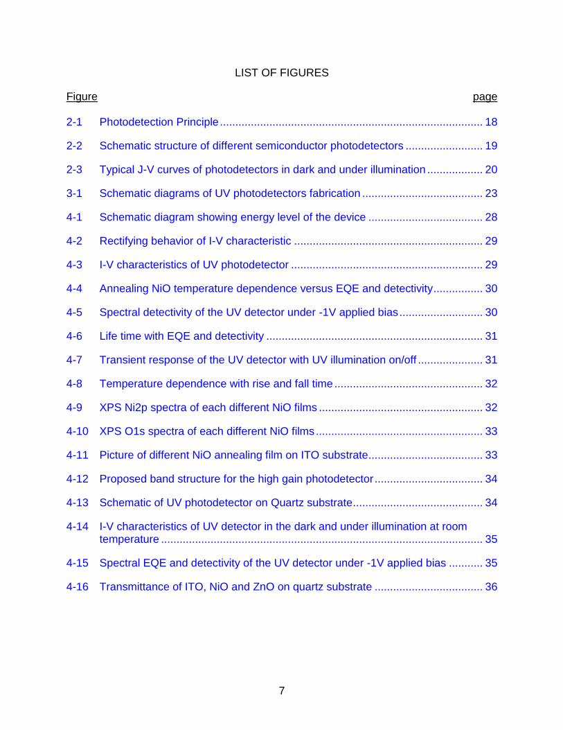
LIST OF FIGURES
Figure page 2-1 Photodetection Principle ..................................................................................... 18
2-2 Schematic structure of different semiconductor photodetectors ......................... 19
2-3 Typical J-V curves of photodetectors in dark and under illumination .................. 20
3-1 Schematic diagrams of UV photodetectors fabrication ....................................... 23
4-1 Schematic diagram showing energy level of the device ..................................... 28
4-2 Rectifying behavior of I-V characteristic ............................................................. 29
4-3 I-V characteristics of UV photodetector .............................................................. 29
4-4 Annealing NiO temperature dependence versus EQE and detectivity ................ 30
4-5 Spectral detectivity of the UV detector under -1V applied bias ........................... 30
4-6 Life time with EQE and detectivity ...................................................................... 31
4-7 Transient response of the UV detector with UV illumination on/off ..................... 31
4-8 Temperature dependence with rise and fall time ................................................ 32
4-9 XPS Ni2p spectra of each different NiO films ..................................................... 32
4-10 XPS O1s spectra of each different NiO films ...................................................... 33
4-11 Picture of different NiO annealing film on ITO substrate ..................................... 33
4-12 Proposed band structure for the high gain photodetector ................................... 34
4-13 Schematic of UV photodetector on Quartz substrate .......................................... 34
4-14 I-V characteristics of UV detector in the dark and under illumination at room temperature ........................................................................................................ 35
4-15 Spectral EQE and detectivity of the UV detector under -1V applied bias ........... 35
4-16 Transmittance of ITO, NiO and ZnO on quartz substrate ................................... 36
8
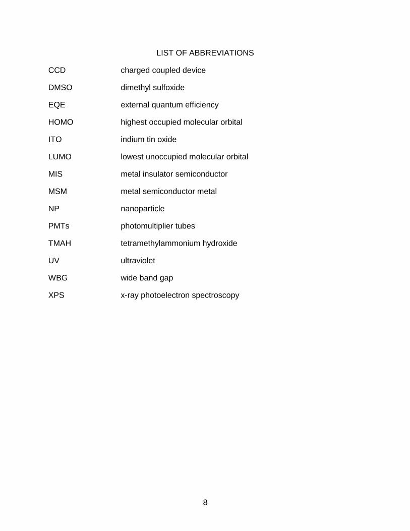
LIST OF ABBREVIATIONS
CCD charged coupled device
DMSO dimethyl sulfoxide
EQE external quantum efficiency
HOMO highest occupied molecular orbital
ITO indium tin oxide
LUMO lowest unoccupied molecular orbital
MIS metal insulator semiconductor
MSM metal semiconductor metal
NP nanoparticle
PMTs photomultiplier tubes
TMAH tetramethylammonium hydroxide
UV ultraviolet
WBG wide band gap
XPS x-ray photoelectron spectroscopy

9
Abstract of Thesis Presented to the Graduate School of the University of Florida in Partial Fulfillment of the Requirements for the Degree of Master of Science
SOLUTION-PROCESSED P-N JUNCTION ULTRAVIOLET PHOTODETECTORS
BASED ON P-NIO AND N-ZNO
By
Jiho Ryu
August 2012
Chair: Franky So Major: Materials Science and Engineering
Ultraviolet (UV) photodetectors have a wide range of applications in the industrial
and military areas, including biological and environmental research, astronomical
studies, missile plum detection, flame sensing, optical communication, and so forth.
Although several UV-detectors have recently been developed using Schottky junction
diodes and pn-junction of wide-gap semiconductors such as ZnS, GaN, ZnSe, and
diamond, these UV photodetectors still have limitations that make them inappropriate
for many applications due to their high cost and low quantum efficiency of less than
40%. In this study, we report on a low cost of solution-processed and high quantum
efficiency UV photodetectors fabricated using solutions of p-type NiO(Eg ~3.7eV) and
ZnO(Eg~3.3eV).
NiO layer as a p-type were deposited on ITO (Indium Tin Oxide) glass by use of a
spin-coat method. Then NiO layers were heated to a temperature at 270℃, 350℃,
450℃, 540℃ for 40 minutes respectively. ZnO nanoparticle(NP) layers as a n-type were
deposited same as NiO layer and heated to a temperature at 100℃ for 10min. An
Aluminum as electrode layer of around 80nm was deposited by thermal evaporation
10
onto the NiO / ZnO layer. This device was investigated by current-voltage (I-V)
characteristics. The devices exhibit the dark current density are 36 nA/cm2, 9.2 nA/cm2,
6.8 nA/cm2, 0.7 nA/cm2 under -1V applied bias and quantum efficiency(QE) are
25,291%, 5,743%, 3,796%, 189% at a wavelength of 350nm with detectivity of 2.08 ×
1013, 9.44 × 10¹², 7.24 × 10¹², 1.11 × 10¹² were achieved at 350nm respectively.

11
CHAPTER 1 MOTIVATION
Many of the important applications of ultraviolet (UV) detection are in high
temperature flame detection, space research, gas sensing, missile warning systems, air
quality monitoring, accurate measurement of radiation for the treatment of UV
exposured skin, etc. [1-4] . The most common detectors recently in use are the
photomultipliers tubes (PMT’s) and the silicon photodetectors, but they are not blind and
demand costly filters to attenuate unwanted and infrared radiation. With the use of wide
band-gap semiconductors such as NiO, GaN, diamond and ZnO, the need for these
filters would be eliminated. Among them, NiO is a well-known transparent p-type
semiconductor with a band gap of about 3.7eV. It has a rock salt cubic structure and a
weak absorption band due to the d–d transition of 3d8 electron configuration in the
visible region [5-7]. Also ZnO, an environmentally friendly semiconductor with a room-
temperature band gap of 3.35 eV, is of great interest for UV detection because of its
various synthetic methods, diverse processing technologies, and the capability of
operating at high temperatures and in harsh environments. Liu et al. fabricated Schottky
UV photodetectors which exhibit fast response speed by growing high quality ZnO
epitaxial films on sapphire substrates [8]. Nevertheless, achieving high crystal quality of
ZnO thin films with suitable metal contacts is still challenging because of the lack of
high-quality and low-cost substrates for lattice-matched growth. Most ZnO thin films
deposited by metal-organic chemical vapor deposition, pulsed laser deposition, or radio
frequency sputtering have a large density of dislocations and grain boundaries.
Transport and UV photoconduction in these polycrystalline ZnO films depends

12
sensitively on stoichiometry, trap densities, and most importantly, gas adsorption and
desorption on the crystal surfaces.
However, solution-processed electronic and optoelectronic devices have some
advantages over conventional crystalline semi-conductor devices in terms of ease of
fabrication, large device area, physical flexibility, and most importantly, low cost.
Therefore, in this paper, we developed the fabrication of pn-junction UV
photodetectors by solution processed p-type NiO and n-typ ZnO NPs on the glass
substrates with pre-patterned indium tin oxide (ITO), followed by annealing in air and
evaporation of Aluminum contacts through a shadow mask.
13
CHAPTER 2 BACKGROUND
2.1 Ultraviolet Radiation
In 1801, the first reveal of ultraviolet (UV) radiation was made, when J W Ritter
discovered that certain chemical reactions were catalyzed by exposure to non-visible
radiation with a shorter wavelength than violet. After that, T Young showed that
chemically active radiation tracked the interference laws in 1804. This observation,
together with the work of many other researchers, made it possible to establish that
visible and UV emissions both were expressions of the same sort of electromagnetic
radiation, solely differing in their wavelength.
These days, it is broadly established that the UV region occupies the spectral
interval of λ = 400–10 nm [9]. It is a greatly ionizing radiation, which triggers many
chemical processes. The most important natural UV source is the Sun. Roughly 9% of
the energy obtained from the Sun at the higher layers of the atmosphere is in the UV
range [10], although the stratospheric ozone layer prevents wave lengths shorter than
280 nm from reaching the Earth’s surface. Besides, remaining UV radiation may be
attenuated by pollution in the low troposphere.
2.1.1 Classification
Ultraviolet radiation (UVR) shows the spectral region within a wavelength interval
[11] of λ = 380 –10 nm (hv = 3.2–124 eV) and the UV spectrum is traditionally separated
into a near region (λ = 380–200 nm, hv = 3.2–6.2 eV) and a far region (λ = 200–10 nm,
hv = 6.2–124 eV). The near region contains as follows:
Long-wavelength UVR (UV-A) at 380-315nm (hv = 3.2-3.9 eV). This is the less energetic range. It stimulates photosynthesis, and is involved in the synthesis of some vitamins and basic biochemical compounds. Overexposure may lead to erythema and premature ageing.
14
Middle-wavelength UVR (UV-B) at 315-280nm (hv = 3.9-4.4 eV). Even though partially absorbed by the ozone layer, this composes 9% of the total UV radiation reaching the Earth’s surface. UV-B exposure is risky for human beings (causing burns, cataracts, erythema, and skin cancer), harmfully affects harvests and enhances the ageing of organic materials.
Short-wavelength UVR (UV-C) at 280-200nm (hv = 4.4-6.2eV). This is the most energetic range, and it is also the more deleterious. However, it is almost completely absorbed by the stratospheric ozone layer.
The following division of the spectrum is frequently used in American publications:
near-UV, 400–300 nm; middle UV, 300–200 nm; far-UV, 200–100nm; extreme UV,
100–10nm [12].
2.1.2 Application of UVR
Biologically active UVR action is used in medicine (solar irradiation of people) and
in agriculture.
Vitamin-synthesizing UVR action is used in biotechnology (synthesis of vitamins
D2 and D3).
Bactericidal UVR action is used in water, air and food disinfection, especially for
long storage and during epidemics, and for disinfection of blood intended for transfusion.
The detection of UV radiation is used in a broad range of military and civil
applications, such as biological and chemical analysis (pollutants, ozone, and most
organic compounds present absorption lines in the UV spectral range), flame detection
(including fire alarms, missile warning or combustion monitoring), optical
communications (particularly inter-satellite communications at λ< 280 nm), emitter
calibration (instrumentation, UV lithography), and astronomical studies.
15
2.2 UV Photodetectors
2.2.1 Semiconductor Photodetectors
In semiconductor photodetectors, photons are absorbed in the semiconductor,
creating electron–hole pairs. These photogenerated carriers are separated by the
electric field, due either to the built-in potential or the applied voltage, producing a
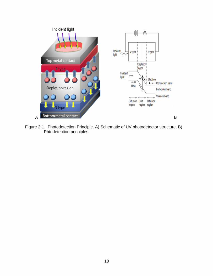
current proportional to the photon flux. The schematic operation of this device is
depicted in Figure 2-1.
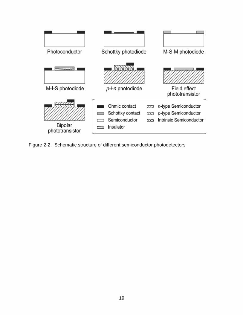
There are different types of semiconductor photodetectors [13]: photoconductors,
Schottky barrier photodiodes, metal–semiconductor–metal (MSM) photodiodes, metal–
insulator–semiconductor (MIS) structures, p–n and p–i–n photodiodes, and field-effect
and bipolar phototransistors. The schematic structure of these devices is depicted in
Figure 2-2.
2.2.2 Semiconductors for UV Photodetection
UV detection has conventionally been achieved by photomultiplier tubes (PMTs),
thermal detectors, narrow-bandgap semiconductor photodiodes or charge-coupled
devices (CCDs). PMTs show low noise and high gain, and can be reasonably visible-
blind. However, they are fragile and bulky devices, demanding high power supplies.
Thermal detectors are normally used for calibration in the UV region. Even though
useful as radiometric standards, these detectors are slow, and their response is
wavelength-independent.
On the other hand, semiconductor photodiodes and CCDs present the benefits of
solid-state devices, demanding only moderate bias. Semiconductor photodetectors are
small, lightweight, and insensitive to magnetic fields. Their good linearity, low cost, and
16
sensibility, and capability for high-speed operation make them a brilliant advance for UV
detection.
Since their well-established technology, ‘UV-enhanced’ silicon photodiodes are the
most common devices for UV photodetection, even though commercial GaAsP and
GaAs based photodiodes are also accessible. Silicon-based UV photodiodes can be
divided into two major families: p–n junction photodiodes and charge-inversion
photodiodes [14, 15].
However, Si-based UV photodiodes exhibit some limitations natural to silicon
technology. The main weak point for these narrow-bandgap semiconductor detectors is
device ageing, since exposure to radiation of much higher energy than the
semiconductor bandgap. Besides, passivation layers, typically SiO2, reduce the QE in
the deep-UV range, and are also degraded by UV illumination. Another limitation of
these devices is their sensitivity to low-energy radiation, so that filters are demanded to
block out visible and infrared photons, resulting in a major loss of effective area of the
instrument. Finally, for high-sensitivity applications, the detector active area must be
cooled to reduce the dark current; the cooled detector behaves as a cold trap for
contaminants, which leads to a lower detectivity.
UV photodetectors based on wide-bandgap (WBG) semiconductors (diamond, SiC,
Ⅲ-nitrides, and some Ⅱ-Ⅴ compounds) are itself a significant benefit for photodetectors,
since it allows room temperature operation, and provides intrinsic visible-blindness [15-
18]. These materials are also apparent that the thermal conductivity of WBG materials is
in general significantly higher than that of silicon, which makes them suitable for high
temperature and high-power applications.
17
In spite of all their promising characteristics, there are still some drawbacks in
WBG semiconductors. The main drawback is crystal quality. The lack of high-quality
substrates for homoepitaxy or other lattice-matched substrates leads to material with a
high density of dislocations and grain boundaries. These structural defects induce
deleterious effects on device performance, such as an enrichment of visible detection
and leakage currents, and the appearance of persistent effects [19, 20].
2.2.3 Photodetector Characterization
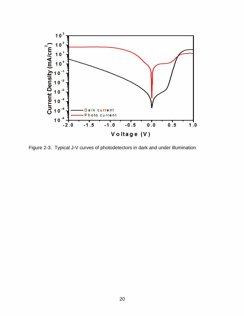
Photodetectors are photodiode with rectifying current density-voltage (J-V)
characteristics. Typical J-V characteristics in the dark and under incident illumination
are shown in Figure 2-3. The responsivity is the most important parameters in
photodetectors and is calculated by the following formula.
R = Jnet photo/Pinc
= (Jphoto-Jdark)/Pinc (1-1)
where Jnet photo (λ) and Pinc (λ) are the net photocurrent, which subtracts the measured
dark current density Jdark (λ) from the measured photo current density Jphoto (λ), of the
photodetector . The quantum efficiency and detectivity can be calculated from the
responsivity using the following expression:
QE = (hc/qλ) × R × 100% (1-2)
D* = Jphoto / Pinc (2qJdark)1/2 (1-3)
where h, c, q, and λ are the Plank constant, speed of light, electronic charge, and the
photon wavelength, respectively.
18
A B
Figure 2-1. Photodetection Principle. A) Schematic of UV photodetector structure. B) Phtodetection principles
19
Figure 2-2. Schematic structure of different semiconductor photodetectors
20
Figure 2-3. Typical J-V curves of photodetectors in dark and under illumination

21
CHAPTER 3 EXPERIMENTAL DETAILS
3.1 NiO Solution
The NiO solution was prepared from a precursor, in which nickel acetate
tetrahydrate were dissolved in ethanol. Ethanolamine was added to the precursor as a
stabilizer in equal molar concentration to nickel acetate tetrahydrate.
3.2 ZnO NPs Solution
We used ZnO NPs (3–5 nm in size), which were synthesized through a sol-gel
process using precursors of zinc acetate and tetramethylammonium hydroxide (TMAH).
For a typical process, the ZnO NPs were synthesized by slowly dropwise addition of a
stoichiometric amount of TMAH dissolved in ethanol (0.5M) to zinc acetate dehydrate
(0.1M) dissolved in dimethyl sulfoxide (DMSO), followed by stirring for an hour. After
that, add ethyl acetate and heptanes to obtain ZnO particles use centrifuge, the ZnO
NPs were dissolved in ethanol and stored under ambient conditions. All solutions were fi
ltered with a 0.45 μm filter.
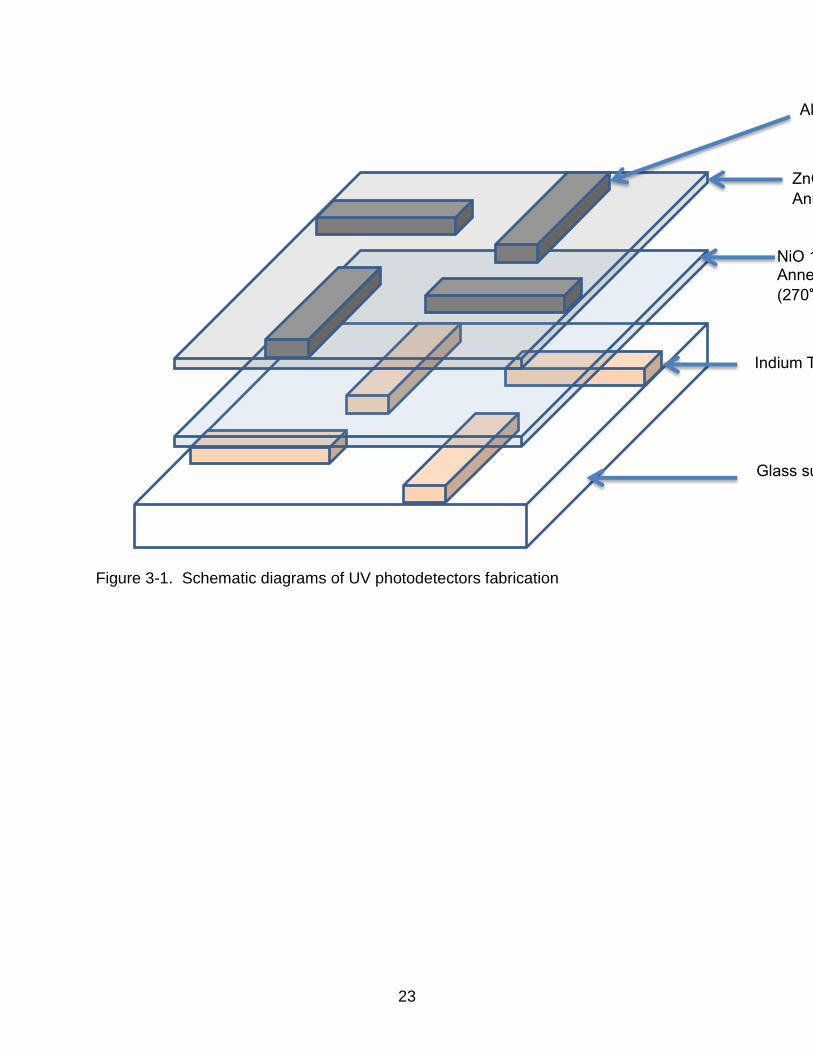
3.3 UV Detectors Fabrication
All UV photodetectors were fabricated on pre-patterned ITO glass substrates with
a sheet resistance of 20 Ω per square. The four ITO glass substrates were first cleaned
with acetone and isopropanol in an ultrasonic cleaner for 15minutes each. And then
blown dry with N2 gas, and subsequently treated with UV ozone for 15 minutes. For p-
type layer, a 130nm thick NiO layer was spin coated on the ITO glass substrates and
the film was subsequently annealed at 270°C, 350°C, 450°C, 540°C for 40min
respectively. After shortly, four samples need to be cool down until 50°C. After that, for
n-type layer, a 70nm thick ZnO layer was spin coated on the four ITO substrates and

22
the film was subsequently baked at 100°C for 10min. ZnO film also need to be cool
down until 50°C. To finish this UV detector fabrication, a 80nm Al was thermally
evaporated on top of ZnO layer as an electrode. This layer was deposited in a vacuum
chamber with a base pressure of 1 × 10⁻⁶ torr. The deposition rate was 2 Å /s for Al. The
active area of the devices used in this study was 0.04 cm2. ITO electrode was always
ground and the Al electrode was applied by negative bias. In addition, the device is also
fabricated on quartz substrate glass. ITO was sputtered on quartz substrate for 15min.
The devices were tested in air without encapsulation. Figure 3-1 shows Schematic
diagrams of UV photodetectors fabrication. The current-voltage (I – V) characteristics of
the devices were measured with a Keithley 4200 semiconductor parameter analyzer.
The devices were irradiated with monochromatic light from a Newport monochromator
using an Oriel solar simulator as a source. Illumination between 300 and 400 nm were
irradiated on the devices with different power intensities (35.6 μWcm−2 and
139μWcm−2, respectively). The illumination intensities at different wavelengths were
measured using two calibrated Newport 918D photodiodes. The EL spectra were
collected using an Ocean Optics HR4000 high-resolution spectrometer. The spectral
response was also used to calculate the spectral detectivity of the devices across the
UV wavelengths. To study the stability of the devices, the unencapsulated
photodetectors were exposed to ambient conditions. The X-ray photoelectron
spectroscopy (XPS) investigations were done on a Perkin Elmer 5100 XPS for NiO film
analysis.
23
Figure 3-1. Schematic diagrams of UV photodetectors fabrication
Glass substrate
Indium Tin Oxide
NiO 130nm(Spin casting) Annealing 40minute
(270℃, 350℃, 450℃, 540℃)
ZnO 70nm(Spin casting)
Annealing 100 ℃ 10min
Al 80nm(Evaporator)
24
CHAPTER 4 RESULTS AND DISCUSSIONS
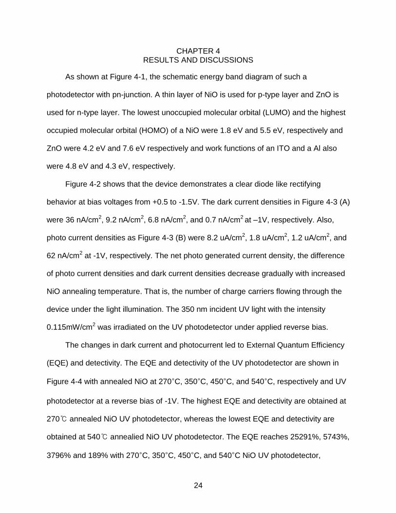
As shown at Figure 4-1, the schematic energy band diagram of such a
photodetector with pn-junction. A thin layer of NiO is used for p-type layer and ZnO is
used for n-type layer. The lowest unoccupied molecular orbital (LUMO) and the highest
occupied molecular orbital (HOMO) of a NiO were 1.8 eV and 5.5 eV, respectively and
ZnO were 4.2 eV and 7.6 eV respectively and work functions of an ITO and a Al also
were 4.8 eV and 4.3 eV, respectively.
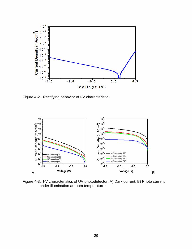
Figure 4-2 shows that the device demonstrates a clear diode like rectifying
behavior at bias voltages from +0.5 to -1.5V. The dark current densities in Figure 4-3 (A)
were 36 nA/cm2, 9.2 nA/cm2, 6.8 nA/cm2, and 0.7 nA/cm2 at –1V, respectively. Also,
photo current densities as Figure 4-3 (B) were 8.2 uA/cm2, 1.8 uA/cm2, 1.2 uA/cm2, and
62 nA/cm2 at -1V, respectively. The net photo generated current density, the difference
of photo current densities and dark current densities decrease gradually with increased
NiO annealing temperature. That is, the number of charge carriers flowing through the
device under the light illumination. The 350 nm incident UV light with the intensity
0.115mW/cm2 was irradiated on the UV photodetector under applied reverse bias.
The changes in dark current and photocurrent led to External Quantum Efficiency
(EQE) and detectivity. The EQE and detectivity of the UV photodetector are shown in
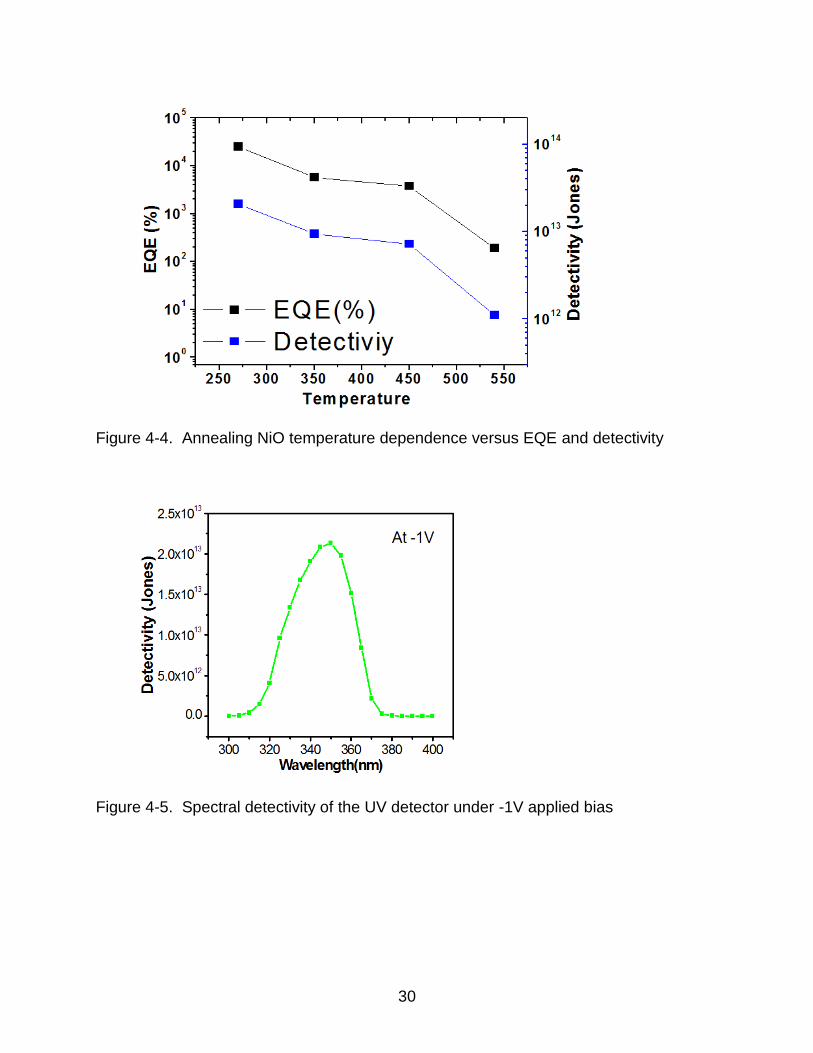
Figure 4-4 with annealed NiO at 270°C, 350°C, 450°C, and 540°C, respectively and UV
photodetector at a reverse bias of -1V. The highest EQE and detectivity are obtained at
270℃ annealed NiO UV photodetector, whereas the lowest EQE and detectivity are
obtained at 540℃ annealied NiO UV photodetector. The EQE reaches 25291%, 5743%,
3796% and 189% with 270°C, 350°C, 450°C, and 540°C NiO UV photodetector,

25
respectively. Also, detectivity (Jones) 2×10¹³, 9.4×10¹², 7.2×10¹², and 1.11×10¹² were
obtained.
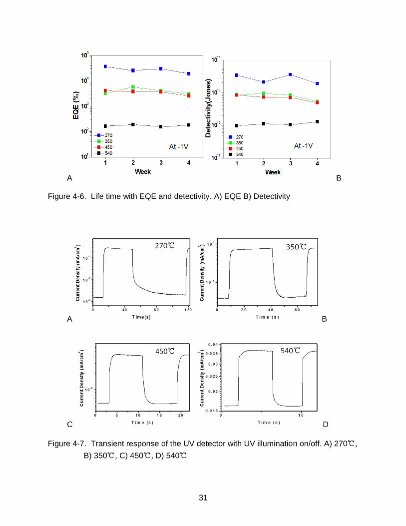
Figure 4-5 illustrates the room-temperature spectral detectivity of UV detector with
NiO annealed at 270°C under -1V applied bias. The spectra show the active range
between 320-365nm. It indicates that this UV detector is visible blindness range. It also
can be seen that cutoff occurred at 320nm due to absorption either ITO and glass
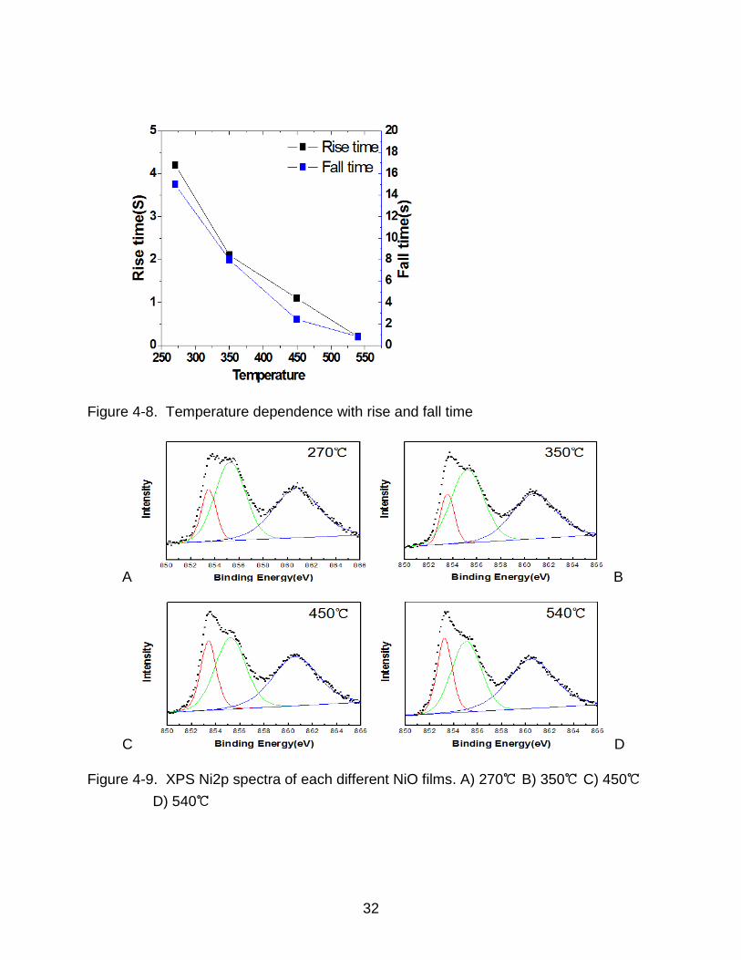
substrate. As shown at Figure 4-6, life time was measured every week for a month. This
UV detector is oxygen based device so the performance of EQE and detectivity for a
month is very stable.
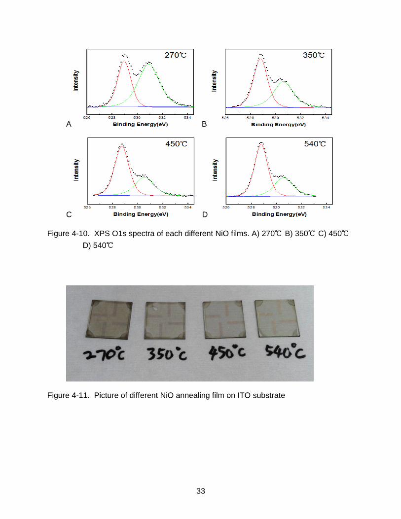
To measure rise time and fall time, the temporal responses of the four detectors
were measured by shutting on/off the light at the wavelength of 350nm under a -1V
applied bias in Figure 4-7. The four detectors exhibited totally different responses. It is
well known that photogenerated electrons will circulate through the external circuit many
times before recombining with hole if those photogenerated holes were trapped by the
surface state at the interface. Consequently, the temporal photocurrent would not drop
sharply when the UV light was turned off like Figure 4-7 (A). This point will discuss later.
As increasing NiO annealing temperature, rise time and fall time is getting be fast in
Figure 4-8.
As can be seen from the above, photo current multiplication occurred at four UV
detectors. At this time, we would like to demonstrate that the photocurrent multiplication
or gain mechanism to be controllable by annealing temperature. Each NiO different
annealing films were measured by X-ray photoelectron spectroscopy (XPS). Figure 4-9
illustrates Ni2p3/2 XPS spectra of each NiO film. For Ni2p3/2 spectra three clearly

26
separated peaks can be detected, which correspond to the binding states of peak NiO
state, peak Ni(OH)2 state and shake-up peak. Red (853.4 eV), green (855.2eV), and
blue peak (860eV) indicate NiO, Ni(OH)2 and shake-up peak, respectively. It can be
seen clearly, that the portion of Ni2p3/2 from Ni(OH)2 is decreasing with the higher NiO
annealing temperature. Ni(OH)2 come from excess of oxygen in surface of NiO film. As
can be seen from Figure 4-10, O1s XPS spectra of each NiO film also show two peaks
such as NiO (528.9eV) and Ni(OH)2. This Figure also shows that Ni(OH)2 peak is
decreasing with the increasing NiO annealing temperature.
It is a well-known fact that NiO that is closely stoichiometric appears green like
nickel oxide solution, whereas material that has an excess of oxygen tends more toward
a black appearance [21]. To illustrate in a quantitative way the nature of this color
change on NiO films picture that were shown in figure 4-11, 270°C NiO film is the
darkest film and 540°C film is the lightest film. Nonstoichiometric NiO (540°C) is the
darkest due to the presence of a lot of Ni3+ ions resulting from the appearance of nickel
vacancies and/or interstitial oxygen in NiO films and have intrinsically p-type conduction
[22, 23]. Nam et al also observed more defective nickel oxide materials containing more
Ni 3+ ion states [24]. Moreover, Lee at al proposed that nonstoichiometric nickel oxide of
Ni3+ ions (directly related to hole concentration) increases with increasing excess of
oxygen, which corresponds to the quantity of Ni2+ ions decreases resulting in a reduced
number of reaction sites for OH- insertion [25].
Now, we can propose why dark current and photo current decrease with
increasing NiO annealing temperature. It has been suggested that the oxidation and
reduction reactions of preexisting Ni3+ ions participate in the storage of charge [26]. It
27
means that Ni3+ Ions can be act as traps of the UV photodetector. Therefore, there can
be a lot of energy level of hole traps near valance band in NiO films. When revere bias
is applied to the device, electrons in valance band can be moved to higher energy band
which is hole traps by thermal exicitation. Then holes generated by thermal excitation
are collected by the applied reverse bias, which correspond to increasing dark current.
For the explanation of photocurrent multiplication, the schematic band diagram as
depicted in figure 4-12 illustrate the condition when the UV detector is under reverse
bias and under UV illumination. The photogenerated holes at ITO / NiO interface are
accumulated [27]. In addition, the accumulation of photogenerated holes near the
interface brings the amount of electrons injected by tunneling barrier under UV
illumination from the ITO electrode occurs.
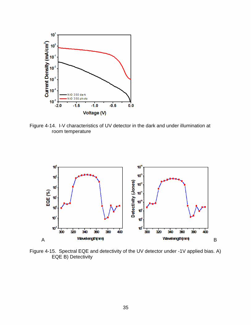
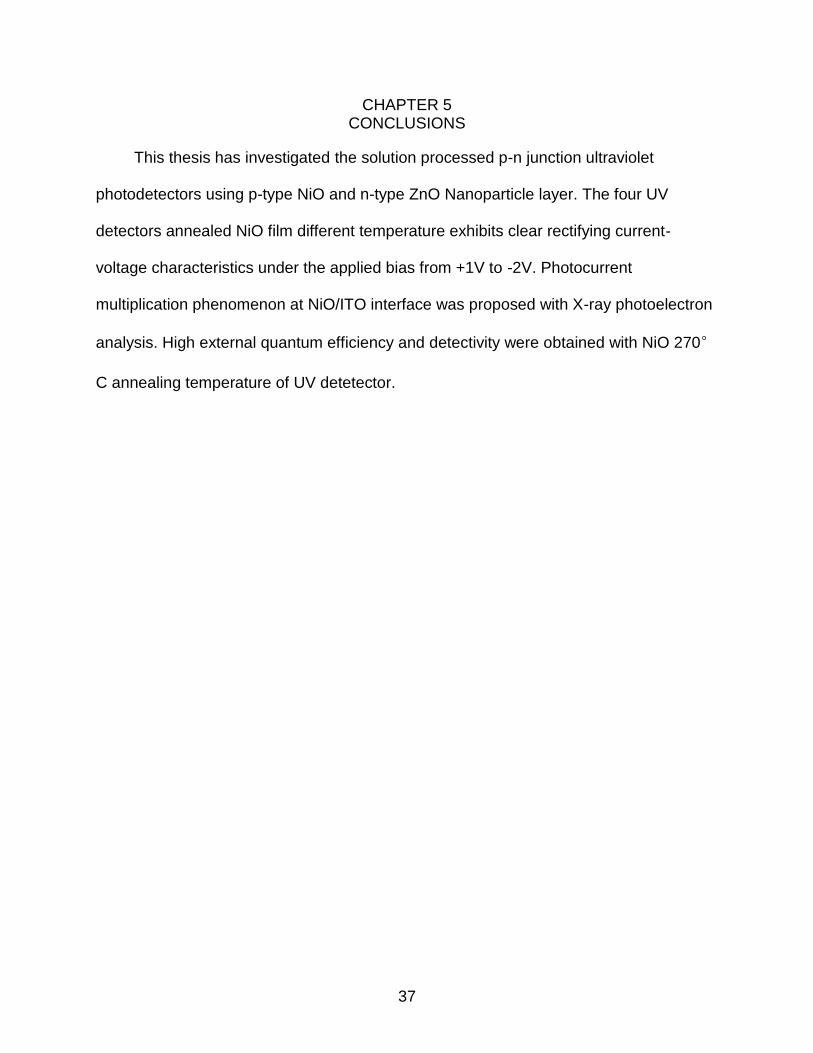
As can be seen from Figure 4-13, UV photodetector was fabricated on quarts
substrate with same procedure to compare between the device with glass substrate and
the device with quartz substrate. The spectral EQE and detectivity were shown in
Figure 4-14. The response range is similar to the UV photodetector on glass substrate.
However, we can clearly observe that peak of EQE and detectivity within range between
300nm-400nm is located 345nm. The peak of detetectivity is little shifted from the UV
detector on glass substrate due to its transmittance. Sharp cut off after 320nm is limited
by ITO electrode. Therefore, UV photodetector response can be wider if electrode is
replaced with shorter absorption such as Ag nanowire.
28
Figure 4-1. Schematic diagram showing energy level of the device
NiO
3.8eV
ITO Al
UV(350nm)
ZnO
3.4eV
1.8
4.2
5.5
7.6
- +
Holes
Electrons
29
Figure 4-2. Rectifying behavior of I-V characteristic
A B
Figure 4-3. I-V characteristics of UV photodetector. A) Dark current. B) Photo current under illumination at room temperature
-1.5 -1.0 -0.5 0.010
-6
10-5
10-4
10-3
10-2
10-1
100
101
102
103
NiO annealing 270
NiO annealing 350
NiO annealing 450
NiO annealing 540
Cu
rren
t D
en
sit
y (
mA
/cm
2)
Voltage (V)
-1.5 -1.0 -0.5 0.010
-6
10-5
10-4
10-3
10-2
10-1
100
101
102
103
NiO annealing 270
NiO annealing 350
NiO annealing 450
NiO annealing 540
Cu
rren
t D
en
sit
y (
mA
/cm
2)
Voltage (V)
30
Figure 4-4. Annealing NiO temperature dependence versus EQE and detectivity
Figure 4-5. Spectral detectivity of the UV detector under -1V applied bias
31
A B
Figure 4-6. Life time with EQE and detectivity. A) EQE B) Detectivity
A B
C D
Figure 4-7. Transient response of the UV detector with UV illumination on/off. A) 270℃,
B) 350℃, C) 450℃, D) 540℃
32
Figure 4-8. Temperature dependence with rise and fall time
A B
C D
Figure 4-9. XPS Ni2p spectra of each different NiO films. A) 270℃ B) 350℃ C) 450℃
D) 540℃
33
A B
C D
Figure 4-10. XPS O1s spectra of each different NiO films. A) 270℃ B) 350℃ C) 450℃
D) 540℃
Figure 4-11. Picture of different NiO annealing film on ITO substrate

34
A B
Figure 4-12. Proposed band structure for the high gain photodetector. A) Dark current mechanism, B) Photo current mechanism
Figure 4-13. Schematic of UV photodetector on Quartz substrate
35
Figure 4-14. I-V characteristics of UV detector in the dark and under illumination at room temperature
A B
Figure 4-15. Spectral EQE and detectivity of the UV detector under -1V applied bias. A) EQE B) Detectivity

36
Figure 4-16. Transmittance of ITO, NiO and ZnO on quartz substrate
37
CHAPTER 5 CONCLUSIONS
This thesis has investigated the solution processed p-n junction ultraviolet
photodetectors using p-type NiO and n-type ZnO Nanoparticle layer. The four UV
detectors annealed NiO film different temperature exhibits clear rectifying current-
voltage characteristics under the applied bias from +1V to -2V. Photocurrent
multiplication phenomenon at NiO/ITO interface was proposed with X-ray photoelectron
analysis. High external quantum efficiency and detectivity were obtained with NiO 270°
C annealing temperature of UV detetector.
38
LIST OF REFERENCES
[1] M. Razeghi, A. Rogalski, J. Appl. Phys. 1998, 79, 7433.
[2] H. Fabricius, T. Skettrup, P. Bisgaard, Appl. Opt. 1986, 25, 2764.
[3] H. Ohta, H. Hosono, Mater. Today. 2004, 7, 42.
[4] T.H. Moon, M.C. Jeong, W. Lee, J.M. Myoung, Appl. Surf. Sci. 2005, 240, 280.
[5] R. J. Powell, W. E. Spicer, Phys. Rev. 1970, B2, 2182.
[6] G. A. Sawatzky, J. W. Allen, Phys. Rev. Lett. 1984, 53, 2339.
[7] A. Fujimori, F. Minami, Phys. Rev. 1984, B30, 957.
[8] S. Liang, H. Sheng,Y. Liu, Z. Huo, Y. Lu, H. Shen, J. Cryst. Growth. 2001,110, 113.
[9] J. Kolnik, I. H. Oguzman, K. F. Brennan, R. Wang, P. P. Ruden, J. Appl. Phys. 1995, 78, 1033.
[10] K. L. Coulson, Solar and Terrestrial Radiation (New York: Academic). 1975.
[11] Russian Standard Photometry. Terms and Definition GOST 26148-84, modification N 1992.
[12] L. R. Koller, Ultraviolet Radiation (New York: Wiley) 1965.
[13] P. Bhattacharya, Semiconductor Optoelectronic Devices (Englewood Cliffs, NJ: Prentice Hall) 1994.
[14] Y. A. Goldberg, Semicond. Sci. Technol. 1999, 14, R41.
[15] M. Razeghi, A. Rogalski, J. Appl. Phys. 1996, 79, 7433.
[16] J. H. Edgar, Properties of Group III Nitrides (London: INSPEC) 1994.
[17] M. N. Yoder, IEEE Trans. 1996, 43, 1633.
[18] S. J. Pearton, J. C. Zolper, R. J. Shul, F. Ren, J. Appl. Phys. 1999, 86, 1.
[19] R. J. McIntyre, J. Appl. Phys. 1961, 32, 983.
[20] A. G. Chynoweth and G. L. Pearson, J. Appl. Phys. 1956, 29, 1103.
[21] R. Newman, and R. M. Chrenko, Phys. Rev. 1959, 1507, 1513.
[22] E. Antolini, J. Mater. Sci. 1992, 27, 3335.
39
[23] H. Sato, T. Minami, S. Takata, T. Yamada, Thin Solid Films 1993, 236, 27.
[24] K. Nam, W. Yoon, K. Kim, Electrochim. Acta. 2002, 47, 3201.
[25] S. Lee, C. Tracy, J. Roland, Electrochim Let. 2004, 7, 10.
[26] V. Srinivasan, J. Weidner, J. Electrochim. Soc. 1997, 144, 8.
[27] K. Nakayama, M. Hiramoto, M. Yokoyama J. Appl. Phys. 2000, 87, 7.
40
BIOGRAPHICAL SKETCH
Ryu, Jiho was born in 1983, in Inje, Republic of Korea. He was curious about how
the images of people were projected on the screen when he watched television as a
student. He eventually looked it up in a children’s encyclopedia. With an incomplete
answer to his question, his curiosity and interest continued to grow from this point. By
the time he was in high school the cellular phone was invented, he wondered how the
liquid crystal display could fit into such a small machine and move around. To answer
this question, he went to Korea Polytechnic University and majored in advanced
materials engineering (2001 – 2008). He concentrated in the field of display, which has
decided his career path. After graduation with B.S. degree, he joined the Department of
Materials Science and Engineering at University of Florida, and completed his M.S.
thesis under the advisory of Dr. Franky So in August 2012. He will start to work for LG
Display as a researcher on September in 2012.