some examples in theory and computation in nano-science sanjay v. khare department of physics and...
TRANSCRIPT

Some examples in theory and computation in nano-science
Sanjay V. Khare Department of Physics and Astonomy
University of ToledoOhio 43606
http://www.physics.utoledo.edu/~khare/

Outline
• About nano-science and technology
• Length Scales and Techniques
• My lines of research, some examples– Dislocation driven surface dynamics– Medium range order in a-Si– Pt-Ru and Pt clusters on carbon, structure and
electronic properties
• Summary
• The Future

The scale of things: Sub-nanometer to Macro
Natural Manmade
Adapted from http://www.sc.doe.gov/bes/

What Happens at the Nanoscale?
Surfaces/interfaces between materials often exhibit different properties (geometric, electronic, and magnetic structure, reactivity, …) from bulk due to broken symmetry and/or lower dimensionality.
New surface and interface properties are the origin of new technological developments:
high-density magnetic recording, phase-change recording, catalysis, “lab-on-a-chip” devices, and biomedical applications (gene therapy, drug delivery and discovery).

What is Nanotechnology?
Activities at the level of atoms and molecules that have applications in the real world.
Nanotechnology encompasses all technical fields.
Key questions:• How can we synthesize a system?• What are the properties (measured and calculated)?• How can we take advantage of them?
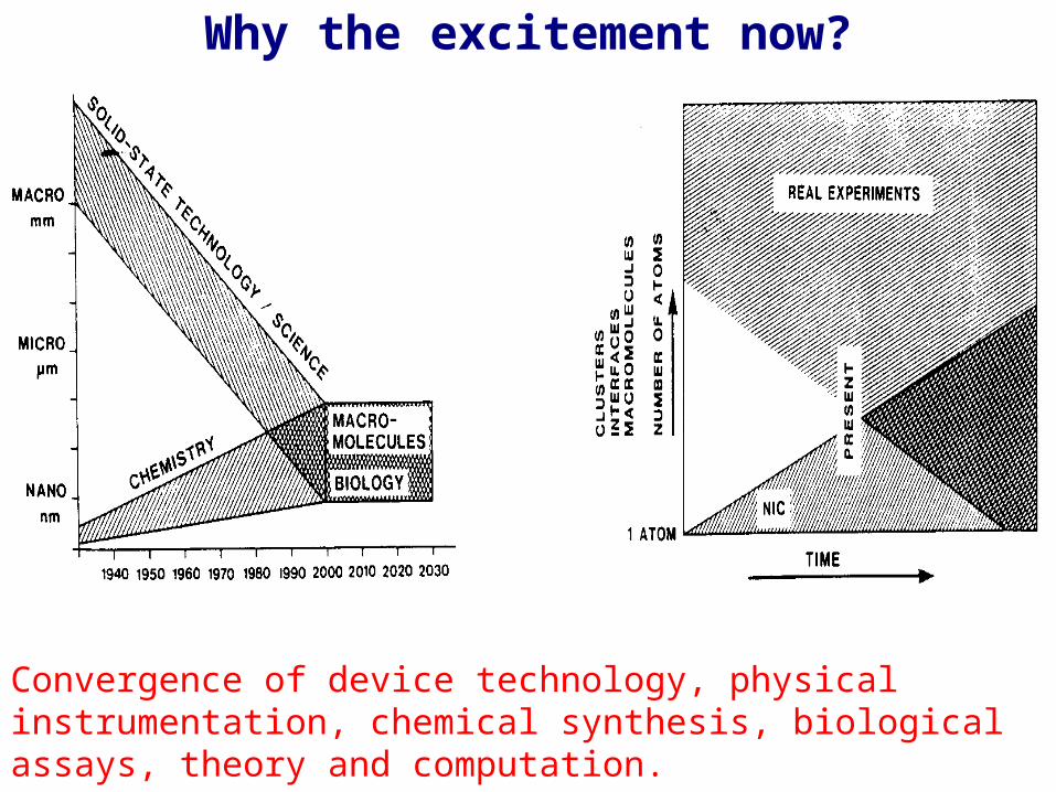
Why the excitement now?
Convergence of device technology, physical instrumentation, chemical synthesis, biological assays, theory and computation.
General theme of my research
Static• Energetic, thermodynamic, electronic, and structural properties
related to materials phenomena.
Dynamic• Near equilibrium and non-equilibrium mass transport
mechanisms at surfaces.
Techniques• Use of appropriate theoretical and computational techniques.
Touch with reality• Direct contact with experiments through explanations,
predictions, and direction for future experimental work.
Theoretical Techniques and Length Scales
• 10 – 100 nm and above: Continuum equations, FEM simulations, numerically solve PDEs, empirical relations.
• 1-10 nm: Monte Carlo Simulations, Molecular Dynamics, empirical potentials.
• < 1 nm Ab initio theory, fully quantum mechanical.
• Integrate appropriate and most important science from lower to higher scale.

Large length scale 100 nm
Length scale: 100 nm Materials: Metals, semiconductors, metal nitrides (Ag, Pt, Si, Ge, TiN)Phenomenon: Energetics, dynamics, fluctuations of steps, islands Techniques: Analytical, Numerical solutions to PDEs, Monte Carlo
Example
Length scale: > 100 nm Materials: surface of TiN(111)Phenomenon: Dislocation driven surface dynamics Techniques: Analytical model

Low energy electron micrographs of decay of two dimensional (2D) TiN islands on TiN(111)
4x4 m2
treal = 12 mintmovie = 17 sec
Ta = 1280 C
Rate of area change dA/dt ~ exp(-Ea/kT),
Ea = activation energy for atom detachment from step to terrace

6.9 7.2 7.5 9.5 10.0 10.5
100
101
102
103
T (K)
dA
/dt
(Å2 /s)
1/kT (eV-1
)
1700 1615 1530 1235 1170 1105
Ea ~ ~ 2.5 eVeV
*S. Kodambaka, V. Petrova, S.V. Khare, D. Gall, A. Rockett, I. Petrov, and J.E. Greene, Phys. Rev. Lett. 89, 176102 (2002).
Measured Ea is in agreement with detachment limited step-curvature driven surface transport**
Rate island area change dA/dt vs. temperature T

field of view: 2.5 mtreal = 90 s; tmovie = 9 s
Low energy electron micrographs of growth of spirals and loops of TiN on TiN(111)
T = 1415 oC
treal = 200 s; tmovie = 21 sfield of view: 1.0
m
T = 1380 oC
Spiral2D Loop
Not BCF growth structures
T/Tm ~ 0.5
2D Loop schematic

• near-equilibrium
• shape-preserving
• period =
• = (2/) ~ ) ~ exp(-Ed/kT), is thermally-activated
• absenceabsence of applied applied stressstress & net mass change net mass change by deposition/evaporation.by deposition/evaporation.
t = 0 s 15 s
31 s 47 s = 47 s= 47 s
TiN(111) spiral step growth
T = 1415 oC
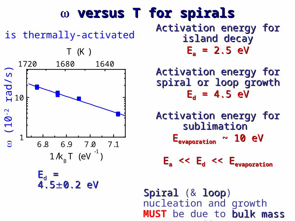
EEdd = 4.5 = 4.50.2 eV0.2 eV
versus T for spiralsversus T for spirals
Activation energy for island decayActivation energy for island decayEEaa = 2.5 eV = 2.5 eV
Activation energy for spiral or loop Activation energy for spiral or loop
growthgrowthEEdd = 4.5 eV = 4.5 eV
Activation energy for sublimation Activation energy for sublimation
EEevaporationevaporation ~ 10 eV ~ 10 eV
EEaa << E << Edd << E << Eevaporationevaporation
SpiralSpiral (& looploop) nucleation and growth MUST be due to bulk mass bulk mass transporttransport !!
6.8 6.9 7.0 7.11
10
T (K)
(1
0-2 r
ad/s
)
1/kBT (eV
-1)
1720 1680 1640
(
10-2 r
ad/s
)
is thermally-activated

Modeling dislocation-driven spiral growthModeling dislocation-driven spiral growth Assumptions:
• driving force: bulk dislocation line energy minimization surface spiral step formation via bulk point defect transport
• dislocation cores emit/absorb point defects at a rate R(T).
rcore
rloopAt steady state: 2
iC (r) 0
eqloop l
core
ooploop
core
s
s
r
r r
r
R
2πD C(r)
k [C
r
(r )-C ]
B.C.s:
C - point defect concentration (1/Å2)
Ds - surface diffusivity (Å2/s)ks - attachment/detachment rate
(Å/s) - area/TiN (Å2)
Step velocity:
eqloop lo
loop
op
loops
dr 1Ω RΩk [C(r ) -
dC =
π r]
2t
constant growth rate dA/dtconstant growth rate dA/dt

Modeling dislocation-driven spiral growth
Analytical model, two key assumptions:
(1) driving force: bulk dislocation line energy minimization surface spiral step formation via bulk point defect transport (2) dislocation cores emit/absorb point defects at a constant rate R(T).
rcore
rloop
Results of model consistent with observations:
(1)(1) Loop or spiral growth rate dA/dt and Loop or spiral growth rate dA/dt and are are constantconstant(2)(2) Both are Both are thermallythermally activatedactivated(3) Activation energy (3) Activation energy EEdd corresponds to facile point defect corresponds to facile point defectmigration along bulk dislocation cores.
R(T)

• TiN(111) step dynamics and the effect of surface-terminated dislocations were studied using LEEM (1200-1500 oC).
• Spiral step growth kinetics: qualitatively & quantitatively different from 2D TiN(111) island decay.
•Mechanism: facile bulk point defect migration along the dislocations (Ed = 4.5±0.2 eV).
“Dislocation Driven Surface Dynamics on Solids”, S. Kodambaka, S. V. Khare, W. Sweich, K. Ohmori, I. Petrov, and J. E. Greene, Nature, 429, 49 (2004). Available at: http://www.physics.utoledo.edu/~khare/pubs/
Spirals Summary

Intermediate length scale 10 nm
Length scale: 10 nm Materials: amorphous semiconductors, disordered metal alloys, silica, (a-Si, a-SiO2, a-Al92Sm8)Phenomenon: Structural properties, order-disorder transition, Techniques: Monte Carlo, Molecular dynamics, Image simulation
Example
Length scale: 10 nm Materials: a-SiPhenomenon: Structural properties of a-Si Techniques: Monte Carlo simulation, image simulationMotivation: Solar cells, medium range order

near B far from B
random ordered clusters
incident electrons
(low variance V(k) in I(k)) (high variance V(k) in I(k))
1413124131231222
2
,,,,,1,
,),( rrrgrrgrgf
QkI
QkIQkV
Measuring MRO by Fluctuation Transmission Electron Microscopy
P. M. Voyles, Ph.D. Thesis, UIUC (2000).

Typical Variance Data
3.0
2.5
2.0
1.5
1.0
0.5
0.70.60.50.40.3
k (Å-1
)
a-Si 1st
peak& c-Si 111
c-Si 220
c-Si 311
a-Si
2nd
peak
500 Å
• 15 Å image resolution• peaks at a-Si diffraction maxima
• average of 8-10 V(k) traces
• error bars: one mean
Courtesy, Nittala et al.

• All materials observed to date, a-Si, a-Ge, a-HfO2, a-Al92Sm8, a-Ge2Sb2Te5 show medium range order. • Hypothesis: PC grains are frozen-in subcritical crystal nuclei
Medium range order (MRO) everywhere
Data for a-Si from Voyles et al.
3.5
3.0
2.5
2.0
1.5
1.0
0.5
0.00.70.60.50.40.3
k (Å-1
)
RMS no H RMS 15 at. % H RMS 20 at. % H
0.08
0.06
0.04
0.02
0.00
V(k
)
0.70.60.50.40.3k (Å
-1)
440 °C 0.2: polycrystalline 350 °C: crystals 300 °C: no crystals 250 °C 200 °C
0.2

Para-crystalline (p-Si) model of a-Si
c-Si nano-crystals
continuous randomnetwork (CRN) matrix
+ =
CRN + nano = p-Si c-Si
Grains are randomlyOrientated and highly strained==> Material is diffraction amorphous.
p-Si has medium range order (MRO)

Algorithm to make p-Si models
1. First place grains of bulk terminated c-Si in a fixed volume V. Atoms in these grains are called grain atoms.
2. Then randomly distribute atoms in the remaining volume to create a correct density of a-Si. These atoms are matrix atoms.
3. Connect all matrix atoms in a perfect 4-fold random network.
4. Sew the grain surfaces to the matrix such that the (grains + matrix) form a perfectly 4-fold coordinated network.
At this stage of construction:
Note bonds can be un-physically large. Bonds are just nearest neighbor tables not chemical bonds!

Modified WWW Dynamics
1. Do bond switches similar to WWW method to lower the energy.
2. Use Monte Carlo probability.
3. Use Keating potential for relaxation and bond switches.
4. After all moves are exhausted anneal at kT = 0.2-0.3 eV.
5. Go back to step 1 till no more convergence can be achieved.
2
ijk
2
0
ikij2
0
22
0
2
ijK 3R
RR8R3β
RR163α
E
ij

Order in Crystalline Si
crystalline Si
Crystalline Si: Each atom has 4 bonds and bond angles are fixed. There is short range order and long range order
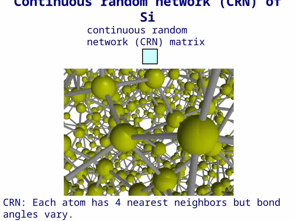
Continuous random network (CRN) of Si
continuous randomnetwork (CRN) matrix
CRN: Each atom has 4 nearest neighbors but bond angles vary. There exists short-range order. But no long range order.

MRO increases smoothly with Ts.
0.08
0.06
0.04
0.02
0.00
V(k
)
0.70.60.50.40.3k (Å
-1)
440 °C 0.2: polycrystalline 350 °C: crystals 300 °C: no crystals 250 °C 200 °C
0.2
Voyles, Gerbi, Treacy, Gibson, Abelson, PRL 86, 5514 (2001)
Change in peak heights ratio with substrate Ts

Questions for theory and modeling
General: How does the structure of the disordered material affect the
V(k) data?
Specific for today: When is the second peak higher than the first?
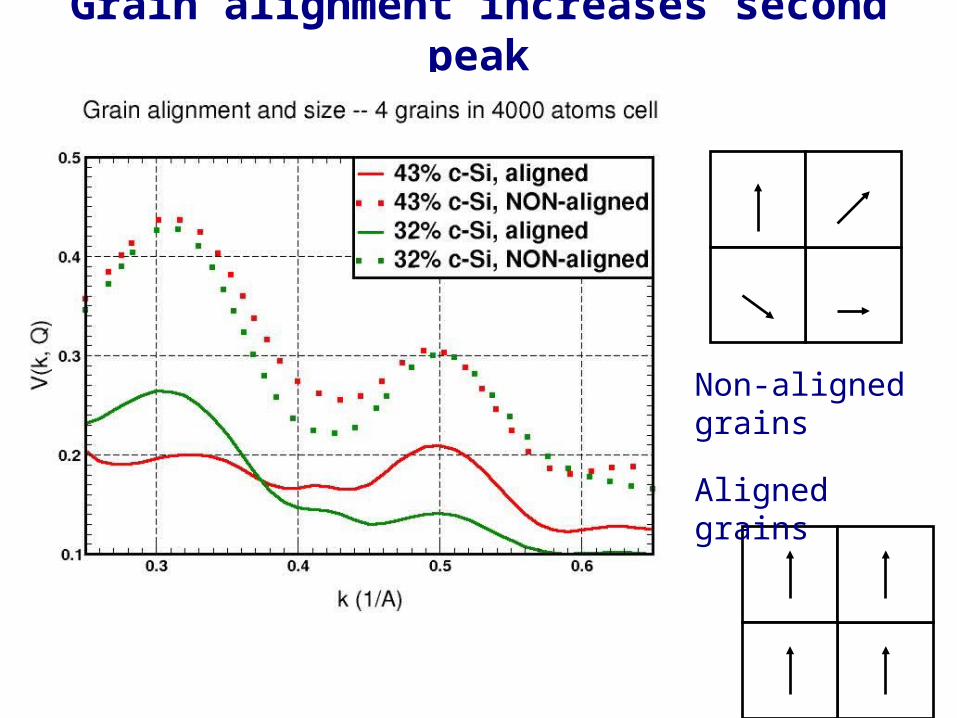
Grain alignment increases second peak
Non-aligned grains
Aligned grains

CRN reduction increases second peak
Big matrix
Small CRNmatrix same grain size

Effect of crystallite shape on relative peak heights
• Large aligned fraction of paracrystalline grains give a higher second peak.
• Similar questions such as dependence of V(k) on grain size distribution can be explained by detailed modeling.
“Evidence from atomistic simulations of fluctuation electron microscopy for preferred local orientations in amorphous silicon,” S. V. Khare, S. M. Nakhmanson, P. M. Voyles, P. Keblinski, and J. R. Abelson, App. Phys. Lett. (85, 745 (2004).
Available at: http://www.physics.utoledo.edu/~khare/pubs/
Synopsis of a-Si modeling

Small length scale 1 nm
Length scale: 1 nm Materials: Metals, semi-conductors (Ag, Pt, Si, Ge, Pt-Ru clusters, Graphite) Phenomenon: Energetics, structural and electronic properties Techniques: Ab initio, molecular dynamics, Image simulation
Example
Length scale: 1 nm Materials: Pt-Ru and Pt clusters on carbonPhenomenon: Structural and electronic properties Techniques: Ab initio methodMotivation: Fuel cells, adsorbate substrate interaction

Motivation and Conclusions• Pure Pt is used extensively as a catalyst
• Pt-Ru alloys are used a catalysts at the anode in fuel cells in the oxidation reaction:
2CO + O2 2CO2
Ru prevents Pt from being poisoned.
• Model system to study binay nano-cluster properties
• Existing experiments at UIUC
• Close-packing geometry preferred by the clusters
• Pt segregates on top of Ru
• Novel substrate mediated effects influence the structure Nanoassemblies are supported for functional “devices”. Supports add (semi-infinite) periodicity and affect properties.

Supported nano-cluster production
PtRu5C(CO) 16 clusters were deposited on various graphitic C surfaces
Pure Pt clusters were deposited on various graphitic C surfaces by a similar process
Topology of both pure Pt and Pt-Ru clusters were then studied using various probes such as STEM, EXAFS, XANES. The structures exhibit a raft like shape

Chemistry of inter-metallic nano-cluster deposition
673 KH2
473 KH2
CO
CO
COC
O
CO
CO
Scheme 1
H2, 673 K
Carbon Black
[PtRu5]/CPtRu5C(CO)16
H2, 673 K
Carbon Black
[PtRu5]/CPtRu5C(CO)16
473 K H2
673 K H2
Nucleation and growth of bimetallic nanoparticles [PtRu5]n from the cluster precursors PtRu5C(CO)5 as observed by EXAFS, occurring on C substrate.
Pt atoms segregate from the core at 400-500 K to the surface at ~700 K.
Experiment: C. W. Hills et al., Langmuir 15, 690 (1999); M. S. Nashner et al., J. Am. Chem. Soc. 120, 8093 (1998); 119, 7760 (1997); A. I. Frenkel et al., J. Phys. Chem B 105, 12689 (2001).

Features of the nano-clusters
10
Cluster order, L
37
185 326
525
92
1 2 3 4 5 6
RuPt
Graphitic carbon support
(2) Cube-octohedral fcc(111) stacking (3) Magic sizes: 10, 37, 92 … atoms
(1) Self-organized nano-clustering on carbon, cluster size 1.0 - 2.0 nm
Pt

Pt goes on top and bulk bond lengths
RuPt
Graphitic carbon support
37 92
Pt92Pt6Ru31
(5) Even small 37 and 92 atom clusters show bond lengths equal to that in the bulk metals, on “inert” graphitic substrate!
(4) In Pt-Ru clusters Pt goes to the top layer

Surprise about bulk bond lengths • Average bond lengths in clusters from the experiment are 99%
- 100%.• In 37 free atom cluster only 8% atoms are fully coordinated. • In 92 free atom cluster only 20% of atoms are fully
coordinated.
37 92
Substrate carbon must be playing a significant role!

Theoretical line of attack
• Must do ab initio to get structure reliably!
• Do Pt/Ru and Ru/Pt complete surfaces with full coverage and clusters
• Cannot do large clusters on graphite with ab initio
• Do large clusters in vacuum only
• Do small ones on graphite and vacuum
• Compare results in vacuum against results on graphite for small clusters
• Compare with experiment

Some checks on our ab initio method
100%99.74%99.36%T/E %
2.453.913.76Theory (T)
2.453.923.78Experiment (E)
C
(Honeycomb
Graphite)
Bulk
Pt
Bulk
Ru
Ab initio theory reproduces bond distances very well!
Table of lattice constants in Å.

Pt on top of Ru always wins theoretically • Simulated cube-octohedral nanocluster of Pt6Ru31 with Pt on top
is stable
• Simulated cube-octohedral nanocluster of Pt6Ru31 with Pt in the middle breaks cube-octohedral symmetry and is unstable
• Theoretically Pt on top wins over Pt sub-surface by 0.31 eV/(surface atom) for hcp(111) Ru surface.
• Theoretically Pt on top wins over Pt sub-surface by 0.48 eV/(surface atom) for fcc(111) Ru surface.
Pt sub-surface Pt on top

Pt6Ru31 neighbour shell distances (Å) Expt. Theory Expt. Theory Expt. Theory
NN shell Pt-Pt Pt-Ru Ru-Ru
1st 2.69 2.70 2.70 2.62 2.67 2.52
2nd 3.78 N/A 3.79 3.71 3.78 3.53
3rd 4.66 4.67 4.70 4.50 4.68 4.41
4th 5.38 5.30 5.40 5.05 5.42 5.12
% of bulk
Both ~ 97% Expt. ~99%
Theory 93-96%
Expt. ~ 100+%
Theory ~ 94-96%
Theory: PtRu simulated in vacuum Expt.: From fits to EXAFS data on CPercentages are comparisons with bulk values

Pt92 neighbour shell distances (Å)
Theory: Pt92 simulated in vacuum Expt.: From fits to EXAFS dataPercentages are comparisons with bulk values
5.96[96.16%]6.18[99.71%]5th
5.34[96.33%]5.52[99.57%]4th
4.67[97.27%]4.78[99.56%]3rd
3.81[97.19%]3.91[99.74%]2nd
2.71[97.77%]2.76[99.57%]1st
Theory [% of bulk]Expt. [ % of bulk]
Pt92NNshell

Small clusters in vacuum and on C
trimer
cappedtrimer
capped10-atom
2.602.652.432.5010
2.772.66bulk
2.552.592.332.484
2.442.522.242.543
2.292.431.902.552
Pt in vacuum
Pt on CRu in vacuum
Ru on C# of atoms
dimer
Average bond lengths in Å from ab initio theory

Bulk-like Bonds: A Substrate-Mediated Effect

Relative scales: Substrate versus Ru
C-C distance ( ) = 1.42 Å , Center to Center( ) = 2.45 ÅRu dimer on C ( ) = 2.54 ÅRu bulk bond length = 2.66 Å
Honeycomb structure of graphene
Substrate length scales < adsorbate scales
Effect of substrate is not just geometric
Lengths not in simple ratios, hence adsorbate clusters are incommensurate
Subtle electronic effect due to graphene electrons

Theory Enhances Understanding
• Nano-assemblies are always substrate-supported
• Substrate mediated effect Properties highly affected by support For metallic nano-clusters on carbon, bond-lengths and distributions agree with experiment once support is included
• Theory yields fundamental insight Location and electronic properties can be analyzed atom by atom Not always possible with simple experiment Experimental data is only simulated to fit with measured signal
• Ab initio methods are reliable for structural and electronic properties!
S. V. Khare, D. D. Johnson et al., (In preparation).

Future theory for catalytic nano-clusters
• Obtain molecular orbital picture of the bonding.
• Study catalysis on Pt-Ru surfaces.
• Investigate other alloy systems which are being discovered such as ceria, tungsten oxide, alumina and others.
• Predict new useful catalytic materials.

Collaborators Senior
Theorists ExperimentalistsD. D. Johnson (UIUC) J. E. Greene (UIUC)
I. Petrov (UIUC) J. R. Abelson (UIUC)
A. A. Rockett (UIUC) R. G. Nuzzo (UIUC)
Colleagues and Students
V. Chirita (U. of Linkoping, Sweden) S. Kodambaka (UIUC)P. Keblinski (RPI) P. M. Voyles (Wisconsin)S. Nakhmanson (NCSU) K. Ohmori (UIUC)
W. Swiech (UIUC) K. Ohmori (UIUC)

Institutional Support
Department of Materials Science and Engineering and Frederick Seitz Materials Research Lab
University of Illinois at Urbana-Champaign Illinois 61801
USA
Support: NSF, DARPA Program, DOE, and ONR.
Exciting future for synergy between theoretical modeling and experiments
• Combination of appropriate theoretical tools for the right length scale and close contact with experimentalists is mutually fruitful!
Thank you!

Z=0.125 Å
Z=0.250 Å
Z=0.375 Å
Z=0.500 Å
Z=0.625 Å
Z=0.750 Å
Z=1.000 Å
Electronic Density Plot: Free Dimer
Free Ru2 bond length = 1.9 Å
Different Z slices

Ru dimer on C slice through Z = 0.80 Å
Electronic Density Plot: Dimer on C
Jahn-Teller distortion: Ru dimer ion cores are not at symmetric hexagon centers.
A single Ru adatom favors hexagon center not side.

Ru dimer on Cslice through Z=0.89 Å
Bottom Ru ion cores is closer to carbon surface.Ru dimer asymmetrically placed in hexagon and canted.
Dimer is canted – not parallel to graphite

Ru trimer on Cslice throughZ=0.18 Å
Electronic Density Plot: Trimer on C
Close to graphite plane
Ru trimer ion cores are not at symmetric hexagon centers.

Charge Difference Isosurface of Planar Ru Trimerrelative to unsupported trimer
±2 e/A3 isosurface redred charge deficityellowyellow charge gain From the bottom
• Symmetry of the charge distribution matches the symmetry of the substrate - lowering energy. As will all 3-fold and 6-fold symmetric clusters.• Hence cub-octahedral stacking occurs on layers that have such symmetry, such a 7-atom layer, …
Courtesy of Lin Lin Wang and D.D. Johnson (UIUC)

Pt6Ru31 Bond Lengths (Å) per n.n. Shell
For Pt92 cluster (5 shells): 99+% in experiment, 96-99% in theory
• 99+% (94-99%) of bulk value in experiment (theory).
• No 2nd n.n. bond for Pt-Pt with Pt atop position!
• Graphite only important for atoms near graphite surface.
673 KH2
473 KH2
CO
CO
COC
O
Scheme 1
H2, 673 K
Carbon Black
[PtRu5]/CPtRu5C(CO)16
H2, 673 K
Carbon Black
[PtRu5]/CPtRu5C(CO)16
473 K H2
673 K H2

Z=1.77 Å
Slice through trimer atoms
Ru trimer is planar, unlike dimer
Average distance from C-graphite remains same as dimer.

Ab initio method details
• LDA, Ceperley-Alder exchange-correlation functional as parameterized by Perdew and Zunger
• Used the VASP code with generalized ultra-soft Vanderbilt pseudo-potentials and plane wave basis set
• 14 Å cubic cell in vacuum with (4x4) graphite surface cell, 7 layers of vacuum
• 18 Ry. energy cut-off with point sampling in the irreducible
Brillouin zone
• Forces converged till < 0.03 eV/ Å
• Used RISC/6000 and DEC alpha machines at UIUC

Self-organized Pt and PtRu nano-assemblies on carbon
Nucleation and growth of bimetallic nanoparticles [PtRu5]n from the cluster precursors PtRu5C(CO)5 as observed by EXAFS, occurring on C substrate.
Pt atoms segregate from the core at 400-500 K to the surface at ~700 K.
RuPt
support

Embedded Atom Method (EAM) details
• Classical potential between atoms made up of a pair potential and an embedding function
• EAM analytical functional for fcc metals from R.A. Johnson, PRB 39,12554(1989)
• EAM potential is well fitted to cohesive energy, bulk modulus, vacancy formation energy and other properties
• Forces converged till < 0.03 eV/ Å
• The potential also yields good surface properties such as the diffusion barrier on Pt(111)

Three areas of my research
Length scale: 100 nm Materials: metals, semiconductors, metal nitrides (Ag, Pt, Si, Ge, TiN)Phenomenon: Energetics, dynamics, fluctuations of steps, islands Techniques: Analytical, Numerical solutions to PDEs, Monte Carlo
Length scale: 10 nm Materials: amorphous semiconductors, disordered metal alloys, silica, (a-Si, a-SiO2, a-Al92Sm8)Phenomenon: Structural properties, order-disorder transition, Techniques: Monte Carlo, Molecular dynamics, Image simulation
Length scale: 1 nm Materials: Metals, semi-conductors (Ag, Pt, Si, Ge, Pt-Ru clusters, Graphite) Phenomenon: Energetics, structural and electronic properties Techniques: Ab initio, molecular dynamics, Image simulation

Density Functional Theory (DFT)
Hohenberg Kohn Theorems (1964)
(1)The external potential of a quantum many body system is uniquely determined by the r), so the total energy is a unique functional of the particle density E = Er)].
(2) The density that minimizes the energy is the ground state density and the energy is the ground state energy,
Min{Er)]} = E0
Synonyms: DFT = Ab initio = First Principles

Kohn Sham Theory (1965)The ground state density of the interacting system of particles can
be calculated as the ground state density of non-interacting particles moving in an effective potential veff r)].
),()()]([2
22
rrrvm nnneff
N
nn rr
1
2)()(
)]([)(
)()]([ 3. rvrd
rr
rrvrv xcnuceff
,)(
)]([)]([
r
rErv xc
xc
Coulomb potential of nuclei
Hartree electrostatic potential
)]([ rExc is universal!
Exchange correlation potential

Practical AlgorithmEffective Schrodinger equation for non-interactng electrons
),()()]([2
22
rrrvm nnneff
,)()(1
2
N
nn rr
Implementation:
1. Guess an initial charge density for N electrons2. Calculate all the contributions to the effective potential3. Solve the Schrodinger equation and find N electron states4. Fill the eigenstates with electrons starting from the bottom5. Calculate the new charge density6. Calculate all the contributions to the effective potential and
iterate until the charge density and effective potential are self-consistent.
7. Then calculate total energy.
N
nnrE
1
)]([

Value of ab initio method• Powerful predictive tool to calculate properties of materials
• Fully first principles ==> – (1) no fitting parameters, use only fundamental constants (e,
h, me, c) as input– (2) Fully quantum mechanical for electrons
• Thousands of materials properties calculated to date
• Used by biochemists, drug designers, geologists, materials scientists, and even astrophysicists!
• Evolved into different varieties for ease of applications
• Awarded chemistry Nobel Prize to W. Kohn and H. Pople 1998

What is it good for?ProsVery good at predicting structural properties: (1) Lattice constant good to 1-10%(2) Bulk modulus good to 1-10%(3) Very robust relative energy ordering between structures(4) Good pressure induced phase changes
Good band structures, electronic propertiesGood phonon spectraGood chemical reaction and bonding pathways
Cons
Computationally intensive, Si band gap is wrongExcited electronic states difficult

Schematic of FEM measurement

Long standing problem: Lack of a technique for direct measurement of Medium Range Order (MRO).
Diffraction is only sensitive to the 2- body correlation function g2(r1,2).
3- and 4-body correlation functions, g3(r12,r13) and g4(r12,r13,r14) carry MRO statistics.
dihedral angle φ
1
2
3
4
FEM measures medium range order MRO

Basis for present work
• Keblinski et al. : Quench from the melt Paracrystallites give V(k) with peaks
• S. Nakhmanson et al. : Modified WWW dynamics Fit one data set for V(k)Studied structural, vibrational, and electronic properties.
•Review: N. Mousseau et al. : Phil. Mag. B 82, 171 (2002).
_________________________________________________
• Present work: Follow Nakhmanson et al. : make family of models.

12 p-Si models + 1 CRN model
% of c-Si atoms
# of c-Si grains
Total # of models
43% 1 or 2 or 4 3
32% 1 or 2 or 4 3
21% 1 or 2 or 4 3
11% 1 or 2 or 4 3
0% 0 1(CRN)
• All models have similar pair-distribution function g2(r).
• All models have bond-angle distribution peaked at 109o ±10o.
• All models have double peaked dihedral angle distribution at 60o and 180o.
All models made of exactly 1000 Si atoms

43% of c-Si differing number of grains

12% of c-Si differing number of grains

Single grain variance differing % of c-Si

Two grain variance differing % of c-Si data

Four grain variance differing % of c-Si

Effect of strain on CRN

Strain effect on single grain data

Strain effect on two grain data