sopc roadmap thomas - pldworld.com · builder sopc builder. sopc 3.0 builder nbuild custom...
TRANSCRIPT


© 2002
Technology RoadmapTechnology Roadmap

Agenda Agenda n Investing in Our Futuren Advanced Process Technologyn Rising Costs of ASIC Development n Core Technology Improvementsn Product Family Roadmapsn Development Toolsn Programmable Systems

© 2002
Investing in Our FutureInvesting in Our Future
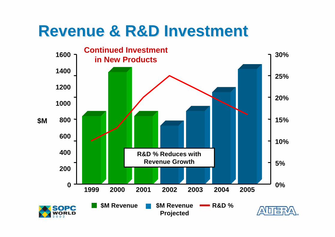
Revenue & R&D InvestmentRevenue & R&D InvestmentContinued Investment
in New Products
$M Revenue $M RevenueProjected
R&D %
$M
0
200
400
600
800
1000
1200
1400
1600
1999 2000 2001 2002 2003 2004 2005 0%
5%
10%
15%
20%
25%
30%
R&D % Reduces with Revenue Growth

Product DevelopmentProduct Development
SOPC
Quartus Development Tools
Architecture Development
IP IntegrationCustomer FeedbackRequirements
§ Process Technology§ Interconnect Structure§ Logic, Memory, I/O§ Hardware Acceleration
§ Hard vs. SoftFunctions§ Cost, Performance,
Power, Complexity§ Stability
§ Design Methodology§ Synthesis, Simulation§ Verification, Debug
§ SOPC Value§ Features, Pricing§ Power, Packaging

Accelerated Architecture Development – 15 MonthsAccelerated Architecture Development – 15 Months
Project Concept
Requirements Refined & Architecture Defined
Beta Software
Design & LayoutComplete
Over 60% of Time Invested with Customers!
First SiliconDecember 2002
September 2002
June 2002
April 2002
October 2001
Customer Requirements Defined
© 2002
Advanced Process TechnologyAdvanced Process Technology

0
0.05
0.01
0.15
0.02
1999 2000 2001 2002 2003 2004
Dra
wn
Gat
e W
idth
(Mic
rons
)
2006
Silicon on Insulator &
Hi-K Dielectric
2005 2007
Source: *International Technology Roadmap for Semiconductors 2001 TSMC 2002 Technology Seminar
0.18 µm
ITRS* Roadmap
45 nm
0.15 µm
0.13 µm
65 nm0.090 µm(90 nm)
TSMC
TSMC Roadmap Outpacing ITRSTSMC Roadmap Outpacing ITRS

0.13µm Status 0.13µm Status n Process
− 9 Layers of Metal− Copper / FSG− High Performance Device− Lithography: 248nm / 193nm
n Altera Ramp Up− 9 Months Production APEX II− Stratix: 4 Products Already Shipped 1S80 ~
230 Million Transistors

Stratix 9-Layer Copper InterconnectStratix 9-Layer Copper Interconnect
12
3456
7
8
9

Stratix Transistor Leff 90nm Stratix Transistor Leff 90nm

90nm Status 300mm Status 90nm Status 300mm Status n Process
− Up to 10 Layers Of Copper− Second Gen. Low-k (K < 3)− Vcc: 1.2V (16A Tox)− Lithography: 193nm
n Project Status− Started In May 2001− Actively Optimizing Process
with TSMC − Process Available Early
2003− Production Targeted 2H
2003
n Development & Qualification Completed in 2001
n Production Ready for 2002-2003 as Demand Increases− Provide Cost Reduction
(Lower Defect Density)

8080
8,086
38680286
Pentium486 Pro
PII
P4
4,004
P3
Technology IntegrationTechnology Integration
1970 1975 1980 1985 1990 1995 2000 2005
1K
10K
100K
1M
10M
100M
Double Density Every 2 Years
ClassicEPM900
MAX5192
FLEX81188
FLEX10K100APEX20400
Stratix1S80APEX20K1500
StratixStratix 1S801S80230M Transistors230M Transistors

© 2002
Rising Costs of ASIC DevelopmentRising Costs of ASIC Development

45 nm0
0.05
0.01
0.15
0.02
1999 2000 2001 2002 2003 2004
Dra
wn
Gat
e W
idth
(Mic
rons
)
0.18 µm
0.15 µm
0.13 µm
65 nm
2006
0.090 µm(90 nm)
2005 2007
TSMC
1.0
2.0
4.0
3.0
$M
Migrationto Extreme Ultraviolet
Source: International Technology Roadmap for Semiconductors 2001TSMC 2002 Technology Seminar
Dramatic Mask Cost IncreaseDramatic Mask Cost Increase
SOI

Increasing Development CostIncreasing Development CostIncreasing Development CostTo
tal D
evel
opm
ent C
ost (
M$)
21
6
In 5 YearsAdvanced TechnologyDevelopment >$20M
18
15
12
9
3
00.18 µm 0.15 µm 0.13 µm 90 nm 65 nm 45 nm
Mask
Test
Layout
Design &Verification
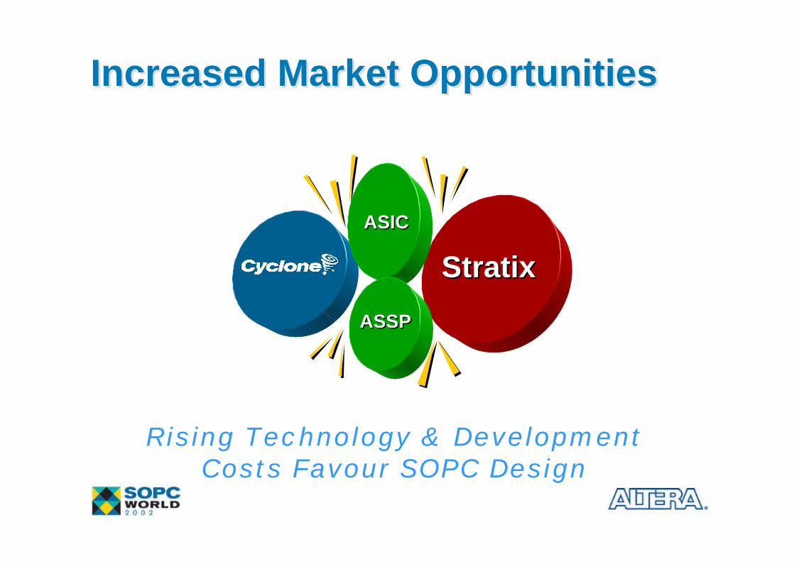
Increased Market OpportunitiesIncreased Market Opportunities
Rising Technology & Development Costs Favour SOPC Design
StratixStratixASSPASSP
ASICASIC
© 2002
Core Technology ImprovementsCore Technology Improvements
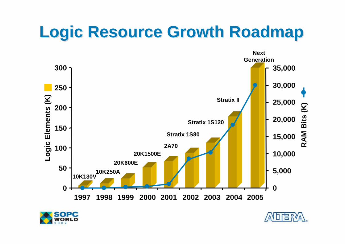
10K130V
Logic Resource Growth RoadmapLogic Resource Growth Roadmap
0
50
100
150
200
250
300
Logi
c El
emen
ts (K
)
1997 1999 2001 2003 20051998 2000 2002 2004
10K250A20K600E
20K1500E2A70
Stratix 1S80
Stratix II
Next Generation
0
5,000
10,000
15,000
20,000
25,000
30,000
35,000
RAM
Bits
(K)
Stratix 1S120

Core Logic EvolutionCore Logic EvolutionCore Logic Evolution
1992 1997 2002 2004
Perf
orm
ance
MercuryMercury
StratixStratix
StratixStratix IIII
§ Tri-Matrix Memory§ Enhanced PLLs§ DSP/MAC Blocks§ On-Chip Termination§ 840 Mbps LVDS§ Hierarchical Clocks
§ Enhanced Memory Features §Fast Arithemetic Functions § DSP/COMM Blocks§ DDRII§ Additional IO Standards§ 1 Gbps LVDS / DPA§ 6.5 Gbps HSSI
FLEX 8000FLEX 8000
APEX 20K
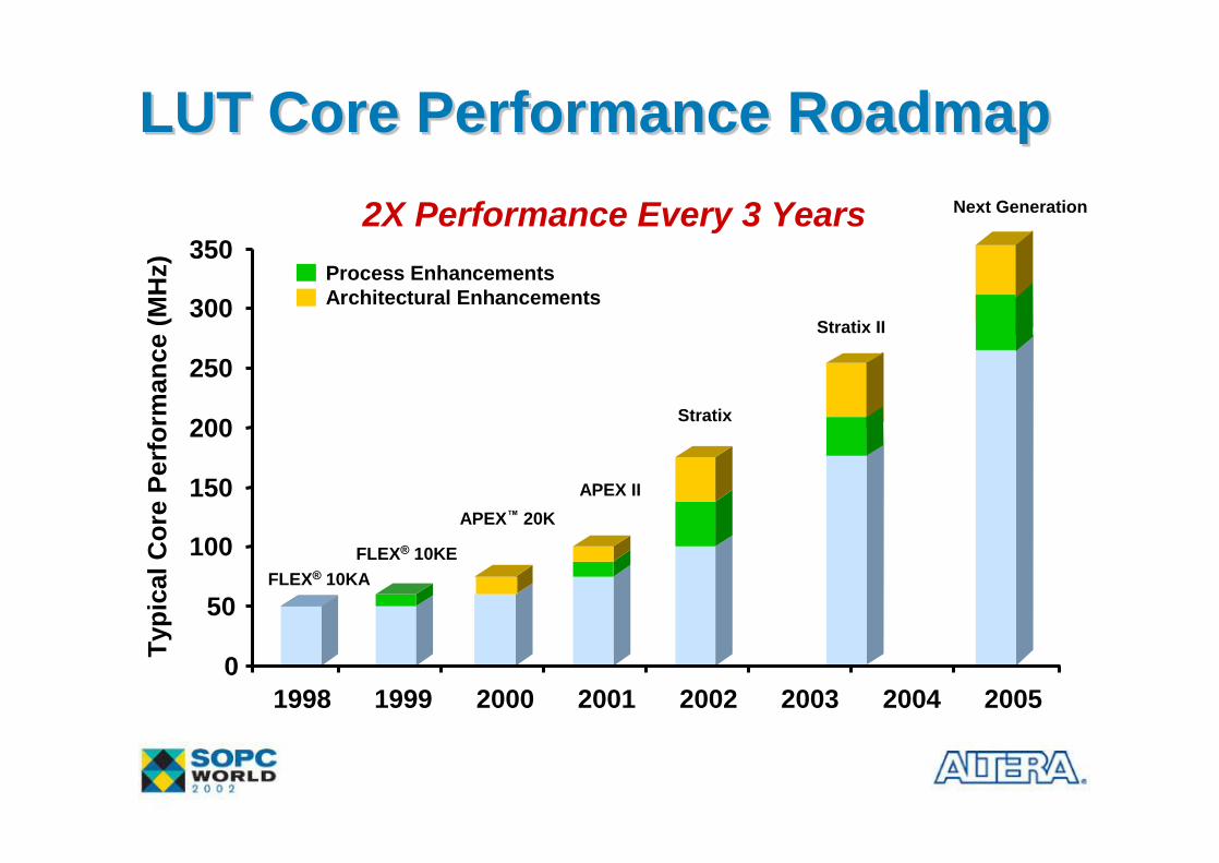
LUT Core Performance RoadmapLUT Core Performance RoadmapLUT Core Performance Roadmap
0
50
100
150
200
250
300
350
Typi
cal C
ore
Perf
orm
ance
(MH
z)
FLEX® 10KA
Process EnhancementsArchitectural Enhancements
1999
FLEX® 10KE
2000
APEX™ 20K
2001
APEX II
1998 2002
Stratix
2004
Stratix II
2X Performance Every 3 Years
2003 2005
Next Generation
High-Speed InterfaceHigh-Speed Interface
1996 1998 2000 2002 2004 2006
Line
Side
(LAN
)B
ackp
lane
Chi
p-to
-C
hip
Gigabit Ethernet1.25 Gbps
10-Gigabit Ethernet
3.125 Gbps4 Channels
40-Gigabit
Ethernet
PL2 PL4PL3
Line Card Interconnect PL5
2.488-3.125 Gbps16 Channels
3GIOPCIRapidIO(Serial)
HyperTransport
I/OInterconnect RapidIO
(Parallel)
2008
< 150 Mbps 1.25 Gbps 2.5 to 3.125 Gbps 5-10 Gbps
1-Gigabit Clock Data Recovery (CDR) Wall

High-Speed I/O RoadmapHigh-Speed I/O Roadmap
Bus Protocols
Electrical Standards
Channel Performance
§ SPI-4 Phase 2§ Gigabit Ethernet§ 1-Gbps Fibre
Channel§ 1-Gbps RapidIO§ 415-Mbps Utopia IV§ 200-MHz CSIX
2001 2002 20042003 2005
1.25 Gbps 3.125 Gbps 6 Gbps 12 Gbps
§ RapidIO Serial/Parallel§ 1G, 2G Fibre Channel§ InfiniBand § 10G Ethernet (XAUI)
LinesideBackplane
§ SONET Backplane
§ 1.25-Gbps CDR § 1.25-Gbps LVDS § 1.25-Gbps PCML§ 1.25-Gbps LVPECL§ 1-Gbps HyperTransport§ 250-MHz HSTL§ PCI-X
§ 3.125-GbpsLVDS With CDR
Architecture Next GenerationStratix GX
Stratix II GX
§ 3.125-GbpsCML With CDR
§ RapidIO §FChannel§ InfiniBand § SPI5, 3GIO§SONNET
§ PAM
§ Chip-Chip§Backplane§ Emerging
High SpeedStandards
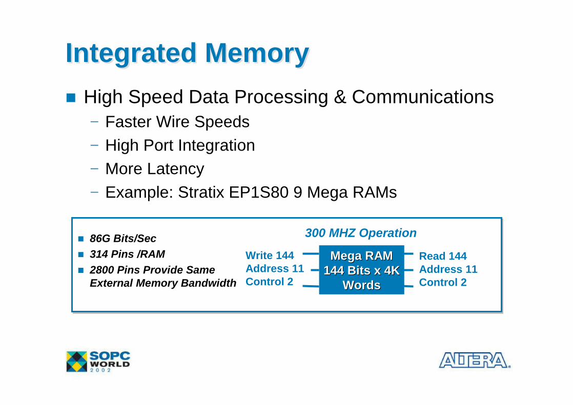
Integrated MemoryIntegrated Memoryn High Speed Data Processing & Communications
− Faster Wire Speeds− High Port Integration− More Latency− Example: Stratix EP1S80 9 Mega RAMs
Mega RAMMega RAM144 Bits x 4K144 Bits x 4K
WordsWords
Write 144Address 11Control 2
Read 144Address 11Control 2
300 MHZ Operationn 86G Bits/Secn 314 Pins /RAMn 2800 Pins Provide Same
External Memory Bandwidth

Embedded Memory RoadmapEmbedded Memory Roadmap
TechnologyPerformance
Features
Architecture Next
GenerationStratix
2001 2002 2003 2004 2005
250 MHz
§ True Dual-Port Mode§ Packing Mode§ Mixed Width
Mode
§ Embedded ShiftRegister Mode§ DDR Mixed
Width Mode§ Three Sizes
of Blocks§ Byte Enable§ Mixed Clock Mode§ Preload
SRAM
300 MHz 550 MHz
SRAM
750 MHz
Stratix II
§EmbeddedCAMs§ Embedded Error
Control Circuitry(ECC)§ High Density
Storage
§ SRAM§ SRAM§ Embedded
DRAM
§ Embedded ErrorControl Circuitry(ECC)§ DDR§ Tri-Matrix
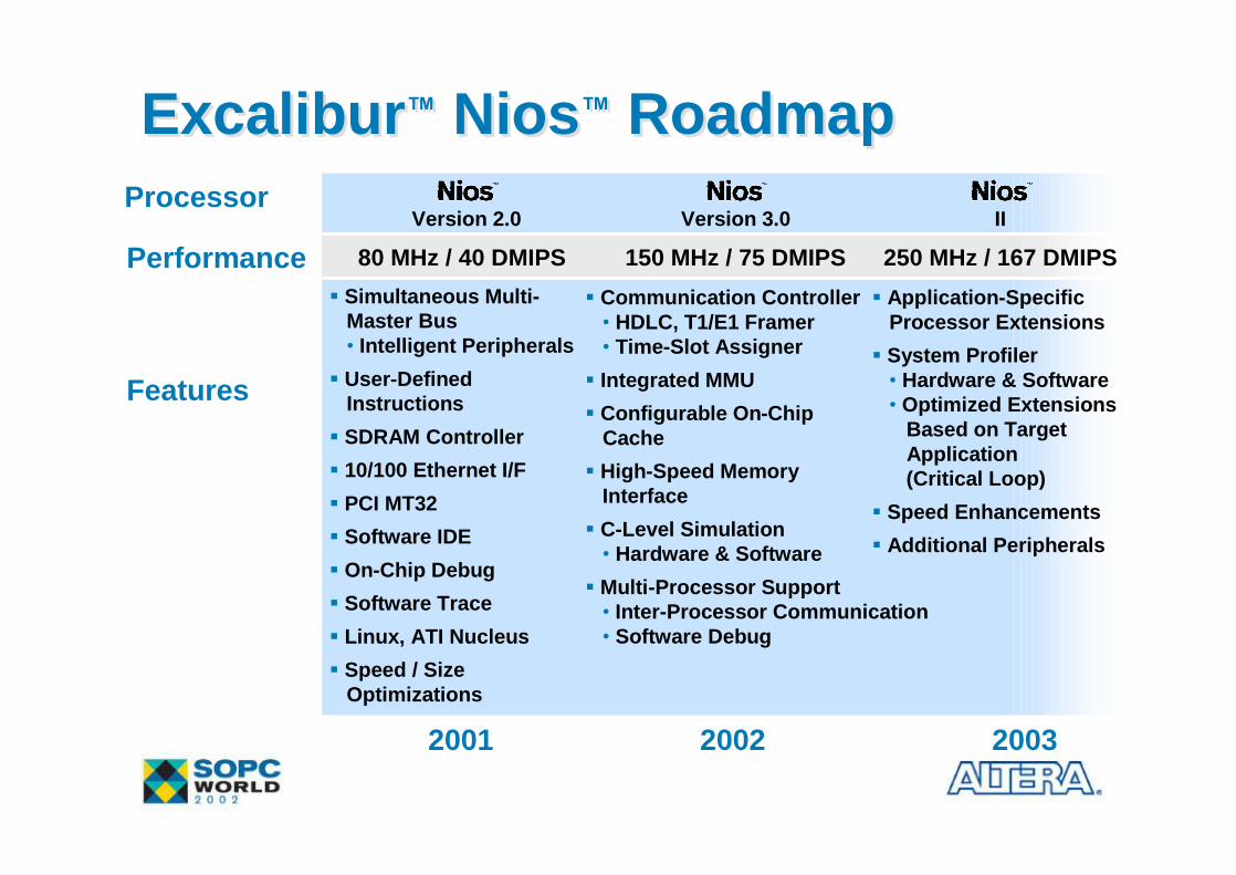
Excalibur™ Nios™ RoadmapExcalibur™ Nios™ RoadmapProcessor
2001 2002 2003
Features
PerformanceVersion 2.0 Version 3.0
80 MHz / 40 DMIPS 150 MHz / 75 DMIPS 250 MHz / 167 DMIPSII
§ Simultaneous Multi-Master Bus• Intelligent Peripherals§ User-Defined
Instructions§ SDRAM Controller§ 10/100 Ethernet I/F§ PCI MT32§ Software IDE§ On-Chip Debug§ Software Trace§ Linux, ATI Nucleus§ Speed / Size
Optimizations
§ Communication Controller• HDLC, T1/E1 Framer• Time-Slot Assigner§ Integrated MMU§ Configurable On-Chip
Cache§ High-Speed Memory
Interface§ C-Level Simulation
• Hardware & Software§ Multi-Processor Support
• Inter-Processor Communication• Software Debug
§ Application-SpecificProcessor Extensions§ System Profiler
• Hardware & Software• Optimized Extensions
Based on Target Application(Critical Loop)
§ Speed Enhancements§ Additional Peripherals
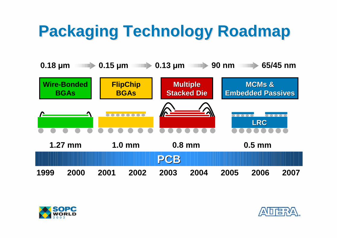
Packaging Technology RoadmapPackaging Technology Roadmap
PCBPCB1999 2000 2007
0.18 µm 0.15 µm 0.13 µm
LRCLRC
90 nm
1.27 mm 0.8 mm 0.5 mm1.0 mm
65/45 nm
20052001 2002 2003 2004 2006
Wire-BondedBGAs
FlipChipBGAs
MultipleMultipleStacked DieStacked Die
MCMsMCMs &&Embedded PassivesEmbedded Passives
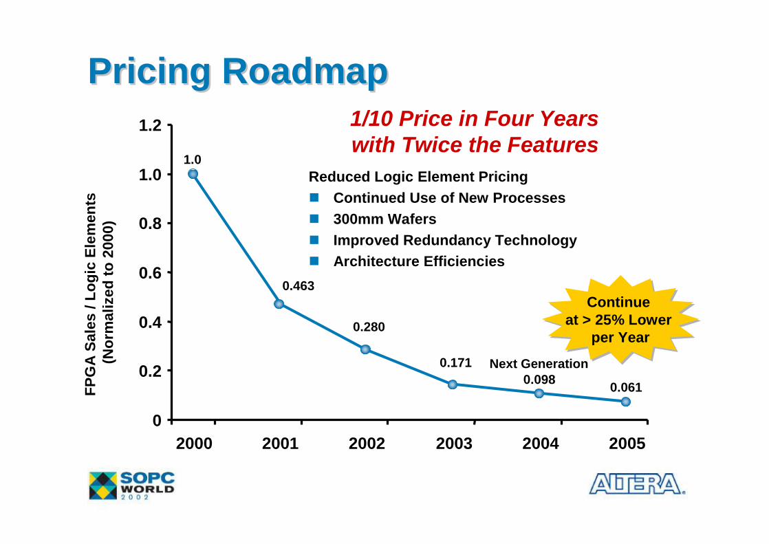
Pricing RoadmapPricing RoadmapPricing Roadmap
0
0.2
0.4
0.6
0.8
1.0
1.2
FPG
A Sa
les
/ Log
ic E
lem
ents
(Nor
mal
ized
to 2
000)
2000
1.0
2001
0.463
2002
0.280
2003
0.171
2004
0.098
2005
0.061
Next Generation
1/10 Price in Four Years with Twice the Features
Reduced Logic Element Pricingn Continued Use of New Processesn 300mm Wafers n Improved Redundancy Technologyn Architecture Efficiencies
Continue at > 25% Lower
per Year
Continue at > 25% Lower
per Year

© 2002
Product Family RoadmapsProduct Family Roadmaps

Altera’s General-Purpose Product PortfolioAltera’s General-Purpose Product Portfolio
Relative Density & Features
Rel
ativ
e C
ost
Addressing Features & Cost

Excalibur
StratixStratix
CycloneCyclone
Stratix GX
PerformancePerformance
CostCost--EffectiveEffective
IP Integration
ACEXACEX
APEXAPEX
Stratix
APEX APEX EAPEX E APEX IIAPEX II
2000 2002 2004
Mercury§ 0.18µ / 0.15µ / 0.13µ§ fMAX = 60-120 MHz§ Max Density = 70K LE§ Embedded RAM = 1.2 MBit Maximum§ Transceiver = 1.25Gbps
§ 0.13µ§ fMAX = 80-175 MHz§ Maximum Density = 100K LE§ Tri-Matrix Memory = 10 Mbit Maximum§ Transceiver = 3.125 Gbps
Excalibur II
Stratix EStratix E
Next Gen.Next Gen.
Perfo
rman
ceStratix II§ 90nm § fMAX = 150-300 MHz§ Max Density = 170K LE§ Memory = 16 Mbit Maximum§ Transceiver = 6.5 Gbps
Altera FPGA RoadmapAltera FPGA RoadmapAltera FPGA Roadmap

MAX3000A
7000B7000B
MAX 3000
MAX 7000§ 0.5µ/0.3/0.22µ Process§ ISP§ tpd = 3.5 ns§ Core = 5 / 3.3 / 2.5V § IO Tolerance = 5 / 3.3 / 2.5 / 1.8V
§ 0.3µ Process§ ISP§ Tpd= 4.5 ns§ Core = 3.3V§ IO Tolerance =5 / 3.3 / 2.5V
Cos
t Red
uctio
n &
Flex
ibilit
y
Future MAX§ 0.18µ Process§ ISP§ Tpd = 3.5 ns§ Core = 3.3 / 2.5 / 1.8V§ IO Tol. = 5 / 3.3 / 2.5 / 1.8V
Altera CPLD RoadmapAltera CPLD Roadmap
7000A
70007000
1987 200520001995 2003
Nex Nex Gen.Gen.5V Core5V Core
2.5V Core2.5V Core
3.3V Core
1.8V Core
Stratix
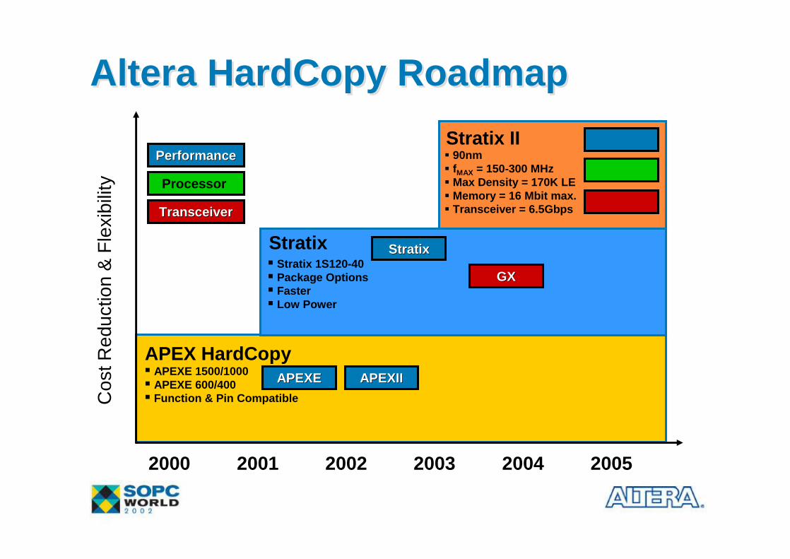
APEX HardCopy§ APEXE 1500/1000§ APEXE 600/400§ Function & Pin Compatible
§ Stratix 1S120-40§ Package Options§ Faster§ Low Power
Stratix II
Altera HardCopy RoadmapAltera HardCopy Roadmap
APEXEAPEXE
2000 200520022001 2003 2004
APEXIIAPEXII
StratixStratix
GXGX
§ 90nm § fMAX = 150-300 MHz§ Max Density = 170K LE§ Memory = 16 Mbit max.§ Transceiver = 6.5Gbps
PerformancePerformance
TransceiverTransceiver
Processor
Cos
t Red
uctio
n &
Flex
ibilit
y

POP QUIZ
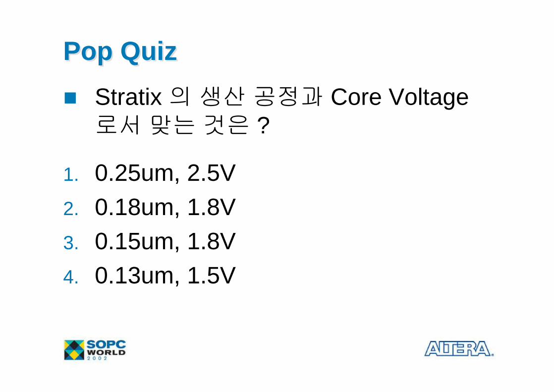
Pop QuizPop Quizn Stratix의생산공정과 Core Voltage 로서맞는것은 ?
1. 0.25um, 2.5V2. 0.18um, 1.8V3. 0.15um, 1.8V4. 0.13um, 1.5V
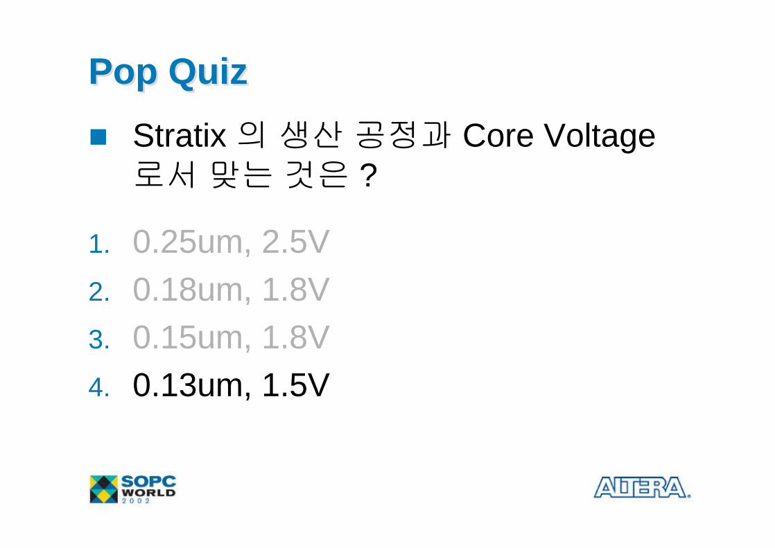
Pop QuizPop Quizn Stratix의생산공정과 Core Voltage 로서맞는것은 ?
1. 0.25um, 2.5V2. 0.18um, 1.8V3. 0.15um, 1.8V4. 0.13um, 1.5V
© 2002
Development ToolsDevelopment Tools

Tools RoadmapTools Roadmapn Altera Will Continue to Focus on Areas
Where We Add Most Valuen Continue to Partner with Leading 3rd
Parties Where They Provide Incremental Expertise & Focus
n SOPC Builder & System Design Automation Will Be Our Major Focus

SOPC Design ToolsSOPC Design Tools
PLD Fabric
SOPC BuilderSOPC
Builder
I/F Architecture
IP
RAMCPU UARTTimer
User Logic
IPUser DSP

SOPC Design ToolsSOPC Design Tools
PLD Fabric
RAMCPU UARTTimer
User Logic
User DSP
I/F Architecture
IP
IP
RAMCPU UARTTimer
EmbeddedSW ToolsetEmbeddedEmbeddedSW ToolsetSW Toolset
MegaWizardMegaMega
WizardWizard
IP
IPDSP BuilderDSP DSP
BuilderBuilderDSP IP DSP IP
User LogicTraditional Synthesis
Flow
Traditional Traditional Synthesis Synthesis
FlowFlow
SOPC BuilderSOPC
Builder

SOPC 3.0 Builder SOPC 3.0 Builder n Build Custom Companion Chip for Your Processor-Based
System with SOPC Builder− Interface to Popular Microprocessors
l PowerPCl TI DSPl PCI
− Custom Peripheral Contentl Communications IPl Signal Processing Algorithms l Memory Interfaces
− Hardware Acceleration Functions l Security IPl Image Processingl Traffic Management / Routing Algorithms

SOPC Builder RoadmapSOPC Builder Roadmap2002
Q1 Q2Q4 Q3
Quartus II v 2.2SOPC Builder 2.7
n Native Synthesis Supportn Cyclone Device Support
2003Q4
Quartus II v. 3.0SOPC Builder 3.0
n External Device Bus Standards
− PowerPC (60x Bus)− TI C6X− PCI
n IP Bus Standards− AMBA− PVCI− Wishbone
n DSP Builder Integrationn Atlantic Bus Supportn SignalTap II Support n Web Update
© 2002
Programmable SystemsProgrammable Systems
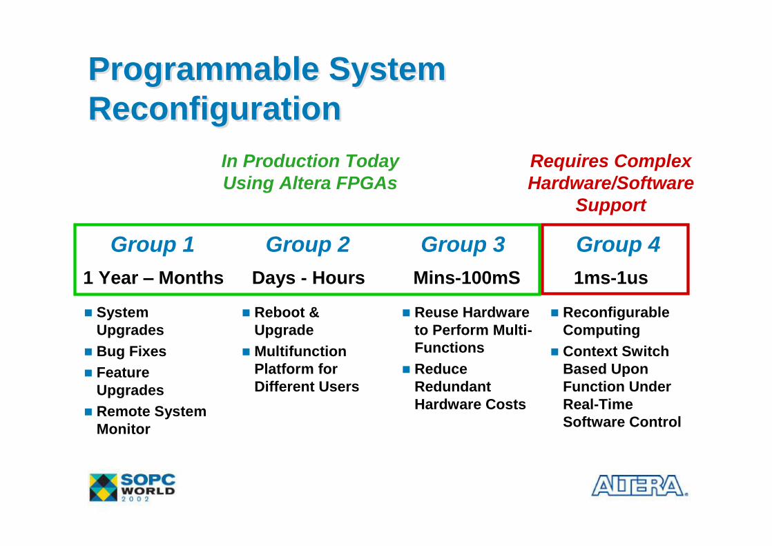
Programmable System ReconfigurationProgrammable System Reconfiguration
1 Year – Months Days - Hours Mins-100mS 1ms-1usGroup 1 Group 2 Group 3 Group 4
n System Upgrades
n Bug Fixesn Feature
Upgradesn Remote System
Monitor
n Reboot & Upgrade
n Multifunction Platform for Different Users
n Reuse Hardware to Perform Multi-Functions
n Reduce Redundant Hardware Costs
n Reconfigurable Computing
n Context Switch Based Upon Function Under Real-Time Software Control
In Production TodayUsing Altera FPGAs
Requires Complex Hardware/Software
Support

n Increasing Use of Remote System Updates
n FPGA Images Uploaded Over Internet or Private Network
n Mainly Using Ethernetn Both System Upgrades &
Remote Monitoring Using Programmability of FPGAs
n Bug Fixes, System Upgrades, New Features
n Significant Cost Advantages over Technician Visit
Re-Configurable SolutionsRe-Configurable Solutions
% Network Attached Applications Using
Remote Updates
Programmable Logic DifferentiatesProduction Solution
0
10
20
30
40
50
60
70
80
90
100
1998 1999 2000 2001 2002 2003 2004 2005
Reconfiguration %

Future System DesignFuture System Design
NetworkPacket
Processor
NetworkPacket
Processor
SRAM
SRAM
Flas
h
DR
AM
FPGAQueueTraffic
DSP
ASSPFramer
O/E
O/E
ASICPolicyEngine
ASSPBP I/F
ASSPBP I/F
DR
AM
Line Side Interface
Bac
k Pl
ane

Future System DesignFuture System Design
NetworkPacket
Processor
NetworkPacket
Processor
SRAM
SRAM
Flas
h
DR
AM
FPGAQueueTraffic
DSP
FPGAFramer
O/E
O/E
FPGAPolicyEngine
FPGABP I/F
FPGABP I/F
DR
AM
Bac
k Pl
ane
n Microprocesorn DSPsn Memoryn SOPCn Analog
− ASIC & ASSPfor High-VolumeProjects

ConclusionsConclusionsn Altera Continues to Innovate & Deliver
Compelling SOPC Solutionsn Focused on Complete Solutions
− Programmable Device Families− Leading Design Automation Tools− Broad Range of IP− Comprehensive Worldwide Technical Support
n Performance, Price, Integration Will Dramatically Expand SOPC Market
Altera SOPC Solution for Rapid Growth