sophie dumas st -ericsson jc42.6 chairman - jedec.org 06 mobile memory forum.pdf · internal bus...
TRANSCRIPT

Sophie DumasSophie DumasSTST--EricssonEricsson
JC42.6 ChairmanJC42.6 Chairman
Mobile Memory Forum: LPDDR3 and WideIOJune 2011

Agenda
• ST-Ericsson: about us…
• Mobile Market Trends drive Low Power DRAM
• JC 42.6 Activities:– LPDDR3
– WideIO
• Questions

ST-Ericsson: about us…
• ST-Ericsson is a leading global supplier of platforms and semiconductors for wireless
• JV owned equally by STMicroelectronics and Ericsson
• Global workforce of 6700 employees with more than 85% of employees in R&D
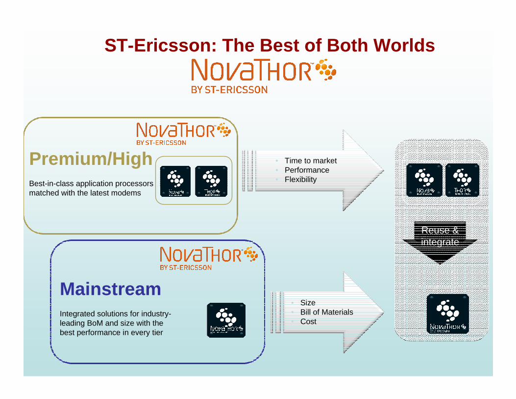
• Time to market • Performance• Flexibility
• Size• Bill of Materials• Cost
Premium/HighBest-in-class application processors matched with the latest modems
MainstreamIntegrated solutions for industry-leading BoM and size with the best performance in every tier
Reuse & integrate
ST-Ericsson: The Best of Both Worlds
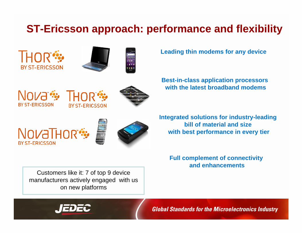
Integrated solutions for industry-leading bill of material and size
with best performance in every tier
Leading thin modems for any device
ST-Ericsson approach: performance and flexibility
Best-in-class application processors with the latest broadband modems
Full complement of connectivity and enhancements
Customers like it: 7 of top 9 device manufacturers actively engaged with us
on new platforms

Mobile Market Trends drive
Low Power DRAM

High Speed Internet
experience
AmazingMobile MarketApplications
4G
Immersive gamingUltra-responsive
user Interfaces
Gesture-controlled UI
AmbientInteraction
Telepresence AugmentedReality
HD cameras and camcorder
Computer Vision
Location-based services
Full HD mediacenter

ARM Core & Low Power DRAM: Parallel Performance Growth
Source : Hynix

Mobile Display: Size and Resolution trends
• Smartphones and Tablet drive display size: WVGA or higher display increasing rapidly• 4.0”or larger display becoming mainstream of smartphones
Display resolution will double (Smartphones) , quad ruple (Tablets)
���� use significant more memory bandwidth
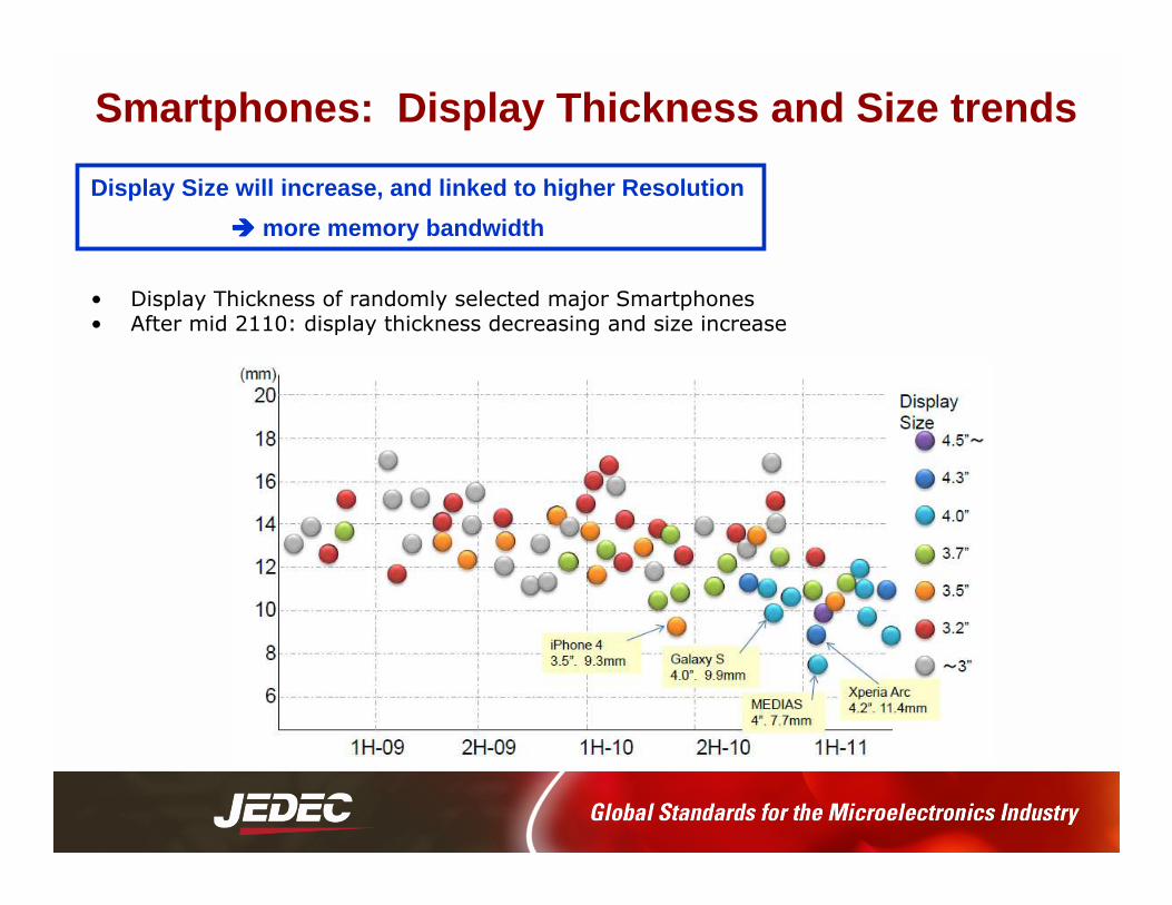
Smartphones: Display Thickness and Size trends
• Display Thickness of randomly selected major Smartphones• After mid 2110: display thickness decreasing and size increase
Display Size will increase, and linked to higher Res olution
���� more memory bandwidth

Video & Display Resolution vs Memory BW
1.6 GBps
3.2 GBps
6.4 GBps
8.5 GBps
12.8 GBps
2010 2011 2012 2013 2014 2015
720pHD 30fpsQHD 0.5 MPix
1080p 30fpsWXGA: 1.2 MPix
1080p 120fps 3DQSXGA 5 MPix
1080p 240 fps 3DQSXGA 5 MPix
Platform Capability (ES)
4.2GB/s
15GB/s
25.8GB/s
1080p 60 fps 3DHD 2 MPix
8.5GB/s
1080p 120fps 3DUXGA 2.4 MPix
12.8GB/s
Dimensioning Use Case:3D video streaming playback to external display via wireless (WiFi or DLNA) + on-line 3D gaming local
Includes: video, graphics and display sub-systems
Source: ST-Ericsson
LPDDR3WideIO SDR
2ch LPDDR2
2GB/s
High graphics and video performance
���� High DRAM BW for Smartphones & Tablets

OS + Applications vs Memory Density
Source: ST-Ericsson, Hynix
2010 2011 2012 2013 2014 2015 Phone (Volume)
1
2
3
Density: GBytes (Typical)
OS Area
Application SW Area
Applications performances
���� Density increase for Smartphones & Tablets
3 GB
1 GB
2 GB

Low Power DRAM Drivers
High Bandwidth & High Density for Smartphones and Tablets driven by:
Video performance increase
Display: High Resolution (HD), stereoscopic (3D)
Graphics: High quality 3D
User Application, multi-tasking
….. impact on DRAM….

After LPDDR2: LPDDR3 and WideIO…
• Graphics performance & Display resolution require higher memory BW in 2013
• ….. BUT quad-channel LPDDR2 is not an option (pin count, power efficiency)
Note: Bandwidth for HOST CPU not includedNote: IO power conditions: LPDDR2 (5pF), LPDDR3 (4pF), WideIO (2-die stack, 2pF)
2011 2012 2013/2014
3.2GBps
5GBps
8.5GBps
12.8GBps
10GBps
1.5 GBps
GXF + Display (GBps) Total Available (GBps)
Dual Channel LPDDR3
@ 800MHz
WideIO@ 200MHz
or
SC LPDDR2 @400MHz
DC LPDDR2 @533MHz80 mW/GBps 70 mW/GBps
40 mW/GBps
DRAM Power / BW

JC-42.6 Activities
Bandw
idth (GB
ps)
LPDDR1
LPDDR2
LPDDR3
12.8
8.5
1.6Pop and Discrete low cost packaging
Low power3D Integration Stacking Technology
DONE
In Progress
WideIOSDR 200
2008 2010 2012 High Volume Ramp Up Devices
DONE
• JC42.6 charter: Low Power DRAM
• Chairman: Sophie Dumas, ST-Ericsson, CTO Office
• 2 active TG: LPDDR3, WideIO

LPDDR3

LPDDR3 positioning
∙ Increased memory BW requirements (graphics, display resolution increase)
∙ LPDDR2 will run out of bandwidth before WideIO is available∙ LPDDR3 fills the gap by upgrading the LPDDR2 standard and supporting
higher operating frequencies
2010 2011 2012 2013 2014 2015
3.2
6.4
9.6
12.8
0.0
MB/s
LPDDR2
LPDDR3
WideIO
LPDDR

LPDDR3 target electrical specification
Parameters LPDDR2 LPDDR3
Clock speed 200-533 MHz 400-800 MHz
Max BW 1 ch (2 ch) 4.2 GBps (8.5 GBps) 6.4 GBps (12.8 GBps)
DRAM array architecture1.2V core with 1.8V wordline
boost=
DRAM IO architecture1.2V, HSUL_12
No DLL in DRAM device=
CLK/DQS scheme Diff/ Bi-dir =
ADD/CMD scheme DDR, single ended =
Data scheme DDR, single ended =
Low Power Modes self-refresh, PASR, DPD =
Internal bus width X128 (4n prefetch) X256 (8n prefetch)
Max density 8 Gbits 32 Gbits
Package POP & MCP =
Burst types BL4, BL8, BL16 BL8

LPDDR3 Benefits
• LPDDR3 is a simple evolution of LPDDR2
• Higher BW than LPDDR2 :– 800 MHz LPDDR3 vs 533 MHz LPDDR2 = +50%
– 667 MHz LPDDR3 vs 533 MHz LPDDR2 = +25%
• LPDDR3 is higher density than LPDDR2
• Equivalent pin-count as LPDDR2
• Lower IO capacitance to improve IO power and SI
• Same BW than WideIO in dual-channel configuration
• Lower assembly and test costs than Wide I/O

LPDDR3 Availability
• LPDDR3 Task Group created in Q4 2010• Dan Skinner, Micron, TG Chair
Wendy Elsasser, Cadence, Vice Chair
• Standard definition is progressing full speed
• Specification target : – Preliminary Spec: Sept 2011 – Final Spec: Dec 2011
• Devices:
2011LPDDR23.2 GBps
2012LPDDR24.3 GBps
2013LPDDR36.4 GBps
2014WideIO
12.8 GBpsExpected Device Mass Production

Wide IO

WideIO Positioning
WideIO offers twice the BW of LPDDR2 for same power
Note: IDD4 (Data toggle 50%), Memory controller + DRAM, LPDDR2 8pF, Wide IO 2pF (2-die stack)
250 530 850
Memory power (mW)
BW (GBps)
LPDDR2x32 @400MHzLPDDR2x32 @400MHzLPDDR2x32 @400MHzLPDDR2x32 @400MHzsinglesinglesinglesingle----channelchannelchannelchannel
3.2
6.4
12.8
WideWideWideWide----IO x512IO x512IO x512IO x512@200MHz (SDR)@200MHz (SDR)@200MHz (SDR)@200MHz (SDR)
quadquadquadquad----channelchannelchannelchannel
8.5LPDDR2x32 @533MHzLPDDR2x32 @533MHzLPDDR2x32 @533MHzLPDDR2x32 @533MHzdualdualdualdual----channelchannelchannelchannel
660
LPDDR2x32 @400MHzLPDDR2x32 @400MHzLPDDR2x32 @400MHzLPDDR2x32 @400MHzquadquadquadquad----channelchannelchannelchannel

WideIO is Low Power
• Reduced interconnect capacitance (TSV) • IO buffering in both SoC and DRAM• Reduced operating frequency • SDR sampling mode
Source : Samsung Wide-IO Memory for Mobile Products - A Deeper Look by i-Micronews
50%
Power Consumption@ same BW
2x LPDDR2 400MHz versus
WideIO SDR 200MHz

Stacking or Hybrid Configurations
Stacking (DRAM Cube) Hybrid
Application WideIO as system memory
-SiP package with DRAM “cube”
-up to 4 stacked dice
Cache memory for multimedia
- SiP bottom package
- FC SoC die (Controller) with TSVs
- Single stacked DRAM
- Additional Memory top package: POP single or dual LPDDR2 (+ flash)
Pros Simple SW & memory Interface in chipset
Small & thin form-factor
High performance (BW & power)
Higher BW
Low Memory cost
Cons High Memory Cost
Maturity in TSV technology
Increases chipset cost (multiple memory IF)
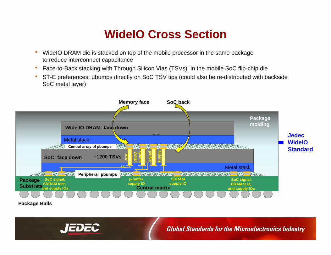
WideIO Cross Section• WideIO DRAM die is stacked on top of the mobile processor in the same package
to reduce interconnect capacitance
• Face-to-Back stacking with Through Silicon Vias (TSVs) in the mobile SoC flip-chip die
• ST-E preferences: µbumps directly on SoC TSV tips (could also be re-distributed with backside SoC metal layer)
JedecWideIO StandardCentral array of µbumps
Metal stackM1
Wide IO DRAM: face down
SoC: face down
PackageSubstrate
sign
al
SDRAMsupply IO
SoC signal,SDRAM test,
and supply IOs
~1200 TSVs test
supp
ly
Central matrix
µ-buffersupply IO
SoC signal,DRAM test,
and supply IOs
VD
DQ
supp
lyMetal stack
Package Balls
SoC backMemory face
Packagemolding
Peripheral µbumps

WideIO electrical specification
• Large bus interface (512 bits) at low frequency (200 MHz) in SDR
• 4 independant and fully asynchronous channels
• BW = 12.8 GBps (200Mbps per pin)
• VDD1 = 1.8V, VDD2 = 1.2V, VDDQ = 1.2V
• Low Power Features: PASR, Auto TCSR
• Balls allocated for future DDR extension
• Total number of balls including supply: 1200 (193/ch signal)
• Density: up to 32 Gbit monolithic
• Up to 4 DRAM dice stacked on top of the mobile processor
• Boundary Scan
• IO physical location – Each channel has 6 rows and 50 columns
– 40µm min pad/bump/TSV pitch
5.27 mm
0.54 mm

Temperature sensors
WideIO µ-bumps
ST-Ericsson WideIO SoC floor plan
- One Smart Memory Engine (SME) per channel- Includes the Network IF + Controller
Channel 0 Channel 1
Channel 3Channel 2
Courtesy of ST-Ericsson

WideIO specification Availability
• WideIO Task Group created in Q4 2008
• DooHee Hwang, Samsung, TG ChairKen Shoemaker, Intel, Vice Chair
• Specification Availability Target : – Preliminary Spec: Sept 2011
– Final Spec: Dec 2011

Thank You!Thank You!

Questions?Questions?