sound processors for home theater system 7.1ch...
TRANSCRIPT

Datasheet
Product structure:Silicon monolithic integrated circuit This product is not designed protection against radioactive rays
1/29 © 2012 ROHM Co., Ltd. All rights reserved. www.rohm.com
TSZ22111・14・001
TSZ02201-0C2C0E100080-1-2017.Sep.2013 Rev.002
Logic
FR Volume
FL Volume
SW Volume
C Volume
SRVolume
SL Volume
SBR Volume
SBLVolume
Modeselector
Rec
ADC
26
25
24
23
22
21
1 2 3 4 5 6 7 8 9 10 11 12 13
20
19
18
17
16
15
14
GS
MG
SM
GS
MG
SM
30 29 28 2734 33 32 3138 37 36 3539
GSMGSMGSMGSMGSMGSMGSMGSMGSMGSMGSMGSM
40
41
42
43
44
45
46
47
48
49
50
51
52
GS
MG
SM
GS
MG
SM
GS
MG
SM
GS
MG
SM
Main
OUTSBR OUTSBLOUTSR OUTSLOUTSW OUTCCLDGND DA
47 µ 0.1µVEE
47µ 0.1 µOUTFR OUTFL
SUBR
SUBL
RECR
RECL
GND
GND
GND
GND
INL8
INR8
INL7
INR7
GND
INL6INR6INL5INR5INL4INR4INL3INR3INL2INR2INL1INR1GND
SBLIN
SBRIN
SLIN
SRIN
CIN
SWIN
FLIN
FRIN
GND
GND
ADCR
ADCL
CHP
VCC
Modeselector
Modeselector
Modeselector
Sub
MULTIINPUT
STEREOINPUT
INR9
INL12
INR12
INL11
INR11
INL10
INR10
INL9
Sound Processors for Home Theater Systems
7.1ch Sound Processor with Built-in Micro-step Volume BD34701KS2
General description
The BD34701KS2 is an 8ch independent volume system. The system is designed in such a way, that it can be used as a 7.1ch surround system. Micro-step volume can reduce the switching shock noise when volume changes, so it can achieve a high-quality set. 8ch dual input selector for zone 2 and multi channel input enable the connection of a number of sources.
Features
8ch input selectors Micro-step volume can reduce the switching shock
noise when volume changes. Zone 2 can support. 2-wire serial bus control, corresponding to 3.3/5V.
Applications
Most suitable for the AV receiver, home theater system
Key Specifications Total harmonic distortion: 0.0004%(Typ.) Maximum output voltage: 4.2Vrms(Typ.) Output noise voltage: 1.5uVrms(Typ.) Residual output noise voltage: 1.0uVrms(Typ.) Cross-talk between channels: -105dB(Typ.) Cross-talk between selectors: -105dB(Typ.)
Package W(Typ.) x D(Typ.) x H(Max.)
SQFP-T52 12.00mm x 12.00mm x 1.50mm
SQFP-T52Typical Application Circuit
Figure 1. Application Circuit

2/29
DatasheetDatasheetBD34701KS2
© 2012 ROHM Co., Ltd. All rights reserved. www.rohm.com
TSZ22111・15・001
TSZ02201-0C2C0E100080-1-217.Sep.2013 Rev.002
17 GND16 GND15 SUBR14 SUBL
VC
C 1
DG
ND
2
DA
3
CL
4
VE
E 5
OU
TFR
6
OU
TFL
7
OU
TSW
8
OU
TC 9
OU
TSR
10
OU
TSL
11
OU
TSB
R 1
2
OU
TSB
L 1
3
18 RECL19 RECR
21 GND20 GND
22 INL823 INR824 INL725 INR726 GND
27 I
NL6
28 I
NR
6
29 I
NL5
30 I
NR
5
31 I
NL4
32 I
NR
4
33 I
NL3
34 I
NR
3
35 I
NL2
36 I
NR
2
37 I
NL1
38 I
NR
1
39 G
ND
SBLIN 40SBRIN 41
SLIN 42SRIN 43
CIN 44SWIN 45FLIN 46FRIN 47GND 48
ADCR 49ADCL 50GND 51CHIP 52
Pin Configuration
Figure 2. Pin Configuration

3/29
DatasheetDatasheetBD34701KS2
© 2012 ROHM Co., Ltd. All rights reserved. www.rohm.com
TSZ22111・15・001
TSZ02201-0C2C0E100080-1-217.Sep.2013 Rev.002
Description of terminal Terminal Number Symbol Function Terminal
Number Symbol Function
1 VCC Positive power supply terminal 27 INL6 Lch input terminal 6
2 DGND Digital ground terminal 28 INR6 Rch input terminal 6
3 DA Data and latch input terminal 29 INL5 Lch input terminal 5
4 CL Clock input terminal 30 INR5 Rch input terminal 5
5 VEE Negative power supply terminal 31 INL4 Lch input terminal 4
6 OUTFR FRch Output terminal 32 INR4 Rch input terminal 4
7 OUTFL FLch Output terminal 33 INL3 Lch input terminal 3
8 OUTSW SWch Output terminal 34 INR3 Rch input terminal 3
9 OUTC Cch Output terminal 35 INL2 Lch input terminal 2
10 OUTSR SRch Output terminal 36 INR2 Rch input terminal 2
11 OUTSL SLch Output terminal 37 INL1 Lch input terminal 1
12 OUTSBR SBRch Output terminal 38 INR1 Rch input terminal 1
13 OUTSBL SBLch Output terminal 39 GND Analog ground terminal
14 SUBL Lch SUB output terminal 40 SBLIN SBLch input terminal for DSP
15 SUBR Rch SUB output terminal 41 SBRIN SBRch input terminal for DSP
16 GND Analog ground terminal 42 SLIN SLch input terminal for DSP
17 GND Analog ground terminal 43 SRIN SRch input terminal for DSP
18 RECL Lch REC output terminal 44 CIN Cch input terminal for DSP
19 RECR Rch REC output terminal 45 SWIN SWch input terminal for DSP
20 GND Analog ground terminal 46 FLIN FLch input terminal for DSP
21 GND Analog ground terminal 47 FRIN FRch input terminal for DSP
22 INL8 Lch input terminal 8 48 GND Analog ground terminal
23 INR8 Rch input terminal 8 49 ADCR Rch output terminal to ADC
24 INL7 Lch input terminal 7 50 ADCL Lch output terminal to ADC
25 INR7 Rch input terminal 7 51 GND Analog ground terminal
26 GND Analog ground terminal 52 CHIP Chip select
4/29
DatasheetDatasheetBD34701KS2
© 2012 ROHM Co., Ltd. All rights reserved. www.rohm.com
TSZ22111・15・001
TSZ02201-0C2C0E100080-1-217.Sep.2013 Rev.002
Logic
FR Volume
FL Volume
SW Volume
C Volume
SRVolume
SL Volume
SBR Volume
SBLVolume
Modeselector
Rec
ADC
26
25
24
23
22
21
1 2 3 4 5 6 7 8 9 10 11 12 13
20
19
18
17
16
15
14
GS
MG
SM
GS
MG
SM
30 29 28 2734 33 32 3138 37 36 3539
GSMGSMGSMGSMGSMGSMGSMGSMGSMGSMGSMGSM
40
41
42
43
44
45
46
47
48
49
50
51
52G
SM
GS
MG
SM
GS
MG
SM
GS
MG
SM
GS
M
Main
Modeselector
Modeselector
Modeselector
Sub
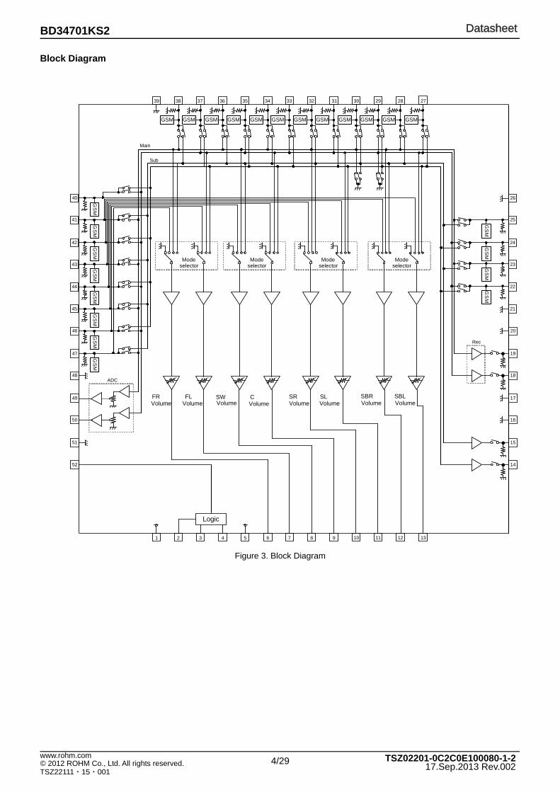
Block Diagram
Figure 3. Block Diagram
5/29
DatasheetDatasheetBD34701KS2
© 2012 ROHM Co., Ltd. All rights reserved. www.rohm.com
TSZ22111・15・001
TSZ02201-0C2C0E100080-1-217.Sep.2013 Rev.002
Absolute Maximum Ratings Item Symbol Rating Unit
Positive power supply Vcc +7.75 (Note1) V
Negative power supply Vee -7.75 (Note1) V
Power dissipation Pd 1.30 (Note2) W
Input voltage Vin Vee-0.2 to Vcc+0.2 V
Operating temperature Topr -40 to +85 (Note3) °C
Storage temperature Tastg -55 to +125 °C (Note1) The maximum voltage that can be applied based on GND. (Note2) This value decreases 13.0mW/°C for Ta=25°C or more. A standard board, 70×70×1.6 mm, shall be mounted. (Note3) If it within operation voltage range, circuit functions operation is guaranteed within operation temp. Caution: Operating the IC over the absolute maximum ratings may damage the IC. The damage can either be a short circuit between pins or an open circuit between pins and the internal circuitry. Therefore, it is important to consider circuit protection measures, such as adding a fuse, in case the IC is operated over the absolute maximum ratings.
Operating Condition
Item Symbol Rating Unit
Positive power supply Vcc +6.5 to +7.5 (Note4,5) V
Negative power supply Vee -6.5 to -7.5 (Note4,5) V (Note4) Applying a voltage based on GND.
(Note5) Within operation temp range, basic circuit function Operation is guaranteed within operation voltage range. But please confirm set up of constant and element, voltage set up and temp set up on use.
Please watch out except condition stipulated by electrical characteristics within the range, It cannot guarantee standard value of electrical characteristics. But it retains original function.

6/29
DatasheetDatasheetBD34701KS2
© 2012 ROHM Co., Ltd. All rights reserved. www.rohm.com
TSZ22111・15・001
TSZ02201-0C2C0E100080-1-217.Sep.2013 Rev.002
Electrical characteristic Unless specified particularly, Ta=25°C, Vcc=7V, Vee=-7V, f=1kHz, Vin=1Vrms, RL=10kΩ, Stereo input selector(MAIN, SUB)=IN1, Mode selector(FL, FRch)=MAIN, Mode selector(SW, C, SL, SRch)=MULTI, Mode selector(SBL, SBRch)=MULTI, Input Att=0dB, Input gain=0dB, Volume=0dB.
Item SymbolLimit
Unit Conditions Min. Typ. Max.
TOTAL
Positive circuit current Iqp - 22 44 mA No signal
Negative circuit current Iqn -44 -22 - mA No signal
Output voltage gain Gv -1.5 0 1.5 dB 6 to 13pin output
Channel balance CB -0.5 0 0.5 dB C Channel reference, 6 to 13pin output
Total harmonic distortion THD - 0.0004 0.02 % BW=400 to 30kHz 6 to 13pin output
Maximum output voltage Vom 3.8 4.2 - VrmsTHD=1%, VOLUME=+10dB 6 to 13pin output
Output noise voltage Vno - 1.5 10 µVrms Rg=0Ω, BW=IHF-A 6 to 13pin output
Residual output noise voltage
Vnor - 1 8 µVrms Volume=Mute, Rg=0Ω, BW=IHF-A 6 to 13pin output
Cross-talk between channels
CT - -105 -80 dB Rg=0Ω, BW=IHF-A 6, 7pin output
Cross-talk between selectors
CS - -105 -80 dB Rg=0Ω, BW=IHF-A 6, 7pin output
Input impedance Rin 32 47 62 kΩ 22 to 25, 27 to 38 40 to 47pin input
VOLUME Maximum attenuation ATTmax - -115 -100 dB Volume=Mute, BW=IHF-A
REC OUT Total harmonic distortion THDR - 0.0005 0.02 %
BW=400 to 30kHz, RL=6.8kΩ 14,15,18,19pin output
7/29
DatasheetDatasheetBD34701KS2
© 2012 ROHM Co., Ltd. All rights reserved. www.rohm.com
TSZ22111・15・001
TSZ02201-0C2C0E100080-1-217.Sep.2013 Rev.002
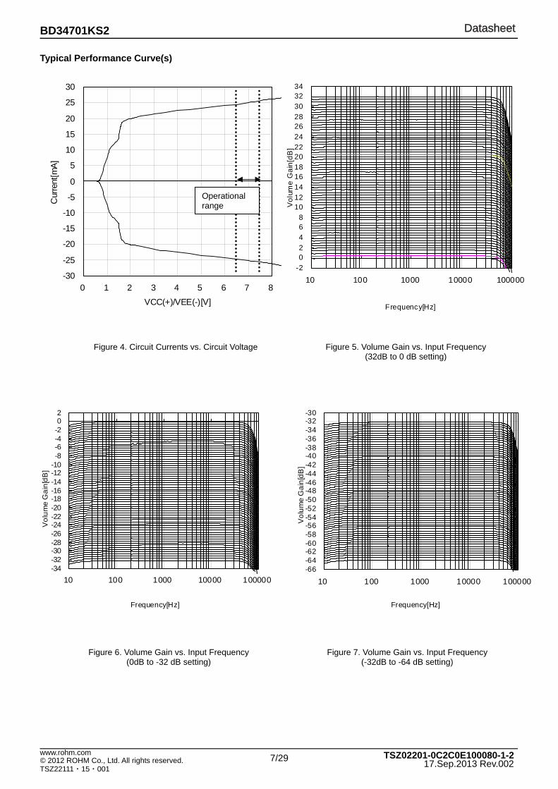
Typical Performance Curve(s)
-30
-25
-20
-15
-10
-5
0
5
10
15
20
25
30
0 1 2 3 4 5 6 7 8VCC(+)/VEE(-)[V]
Cur
rent
[mA]
Figure 4. Circuit Currents vs. Circuit Voltage Figure 5. Volume Gain vs. Input Frequency (32dB to 0 dB setting)
Operational range
Figure 6. Volume Gain vs. Input Frequency (0dB to -32 dB setting)
Figure 7. Volume Gain vs. Input Frequency (-32dB to -64 dB setting)
-202468
10121416182022242628303234
10 100 1000 10000 100000
Frequency[Hz]
Vol
ume
Gai
n[dB
]
-34-32-30-28-26-24-22-20-18-16-14-12-10-8-6-4-202
10 100 1000 10000 100000
Frequency[Hz]
Vol
ume
Gai
n[dB
]
-66-64-62-60-58-56-54-52-50-48-46-44-42-40-38-36-34-32-30
10 100 1000 10000 100000
Frequency[Hz]
Vol
ume
Gai
n[dB
]
8/29
DatasheetDatasheetBD34701KS2
© 2012 ROHM Co., Ltd. All rights reserved. www.rohm.com
TSZ22111・15・001
TSZ02201-0C2C0E100080-1-217.Sep.2013 Rev.002
-98-96-94-92-90-88-86-84-82-80-78-76-74-72-70-68-66-64-62-60
10 100 1000 10000 100000
Frequency[Hz]
Vol
ume
Gai
n[dB
]
0.0001
0.0010
0.0100
0.1000
1.0000
0.001 0.010 0.100 1.000 10.000
Input Voltage [Vrms]
THD
+N[%
]
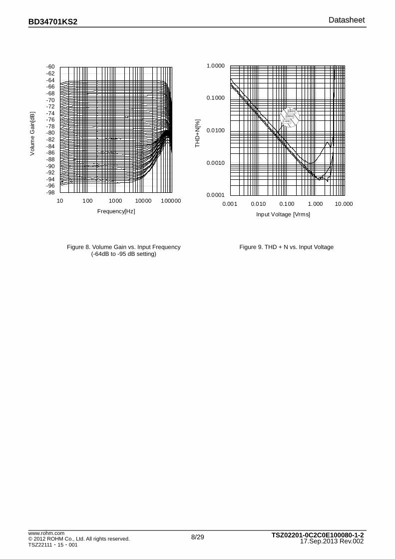
Figure 8. Volume Gain vs. Input Frequency (-64dB to -95 dB setting)
Figure 9. THD + N vs. Input Voltage
10kHz
1 kHz
100Hz
9/29
DatasheetDatasheetBD34701KS2
© 2012 ROHM Co., Ltd. All rights reserved. www.rohm.com
TSZ22111・15・001
TSZ02201-0C2C0E100080-1-217.Sep.2013 Rev.002
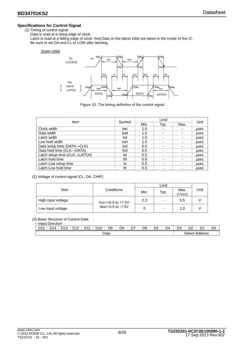
Specifications for Control Signal (1) Timing of control signal
Data is read at a rising edge of clock. Latch is read at a falling edge of clock. And Data on the latest 16bit are taken in the inside of this IC. Be sure to set DA and CL to LOW after latching.
1byte=16bit
Item Symbol Limit Unit Min. Typ. Max. Clock width twc 1.0 - - µsec Data width twd 1.0 - - µsec Latch width twl 1.0 - - µsec Low hold width twh 1.0 - - µsec Data setup time (DATA→CLK) tsd 0.5 - - µsec Data hold time (CLK→DATA) thd 0.5 - - µsec Latch setup time (CLK→LATCH) tsl 0.5 - - µsec Latch hold time thl 0.5 - - µsec Latch Low setup time ts 0.5 - - µsec Latch Low hold time th 0.5 - - µsec
(2) Voltage of control signal (CL, DA, CHIP)
Item Conditions Limit
Unit Min. Typ. Max. (<Vcc)
High input voltage Vcc=+6.5 to +7.5V Vee=-6.5 to -7.5V
2.3 - 5.5 V
Low input voltage 0 - 1.0 V
(3) Basic Structure of Control Data
←Input Direction
D15 D14 D13 D12 D11 D10 D9 D8 D7 D6 D5 D4 D3 D2 D1 D0
Data Select Address
Figure 10. The timing definition of the control signal.
CL
( CLOCK)
DA DATA LATCH
thd thd th ts tsl thl tsd
twc
twh twd twl
tsu
DATA DATA LATCH
90% 90% 90% 90%
10% 10% 10%
90% 90% 90% 90% 90%
10% 10% 10%
twc
10/29
DatasheetDatasheetBD34701KS2
© 2012 ROHM Co., Ltd. All rights reserved. www.rohm.com
TSZ22111・15・001
TSZ02201-0C2C0E100080-1-217.Sep.2013 Rev.002
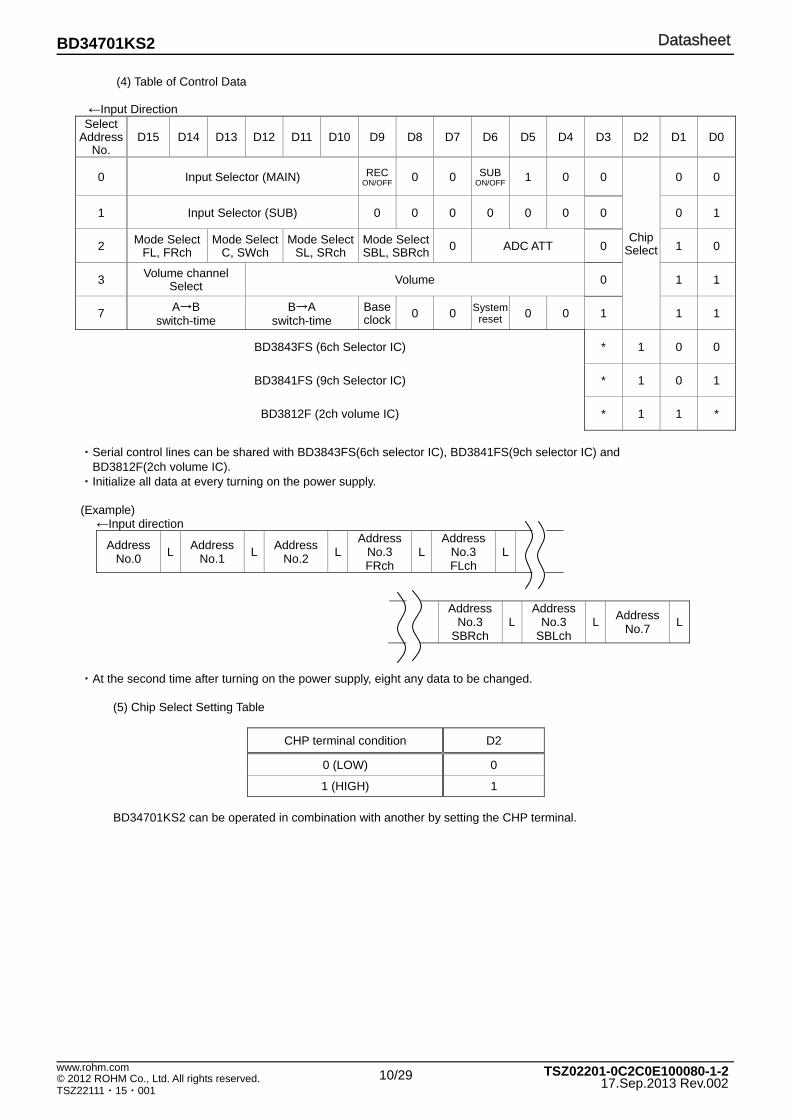
(4) Table of Control Data
←Input Direction Select
Address No.
D15 D14 D13 D12 D11 D10 D9 D8 D7 D6 D5 D4 D3 D2 D1 D0
0 Input Selector (MAIN) RECON/OFF 0 0 SUB
ON/OFF 1 0 0
Chip Select
0 0
1 Input Selector (SUB) 0 0 0 0 0 0 0 0 1
2 Mode Select FL, FRch
Mode Select C, SWch
Mode SelectSL, SRch
Mode SelectSBL, SBRch 0 ADC ATT 0 1 0
3 Volume channel Select Volume 0 1 1
7 A→B switch-time
B→A switch-time
Baseclock 0 0 System
reset 0 0 1 1 1
BD3843FS (6ch Selector IC) * 1 0 0
BD3841FS (9ch Selector IC) * 1 0 1
BD3812F (2ch volume IC) * 1 1 *
・Serial control lines can be shared with BD3843FS(6ch selector IC), BD3841FS(9ch selector IC) and
BD3812F(2ch volume IC). ・Initialize all data at every turning on the power supply.
(Example)
←Input direction
Address No.0 L Address
No.1 L Address No.2 L
AddressNo.3 FRch
LAddress
No.3 FLch
L
AddressNo.3
SBRch L
Address No.3
SBLch L Address
No.7 L
・At the second time after turning on the power supply, eight any data to be changed.
(5) Chip Select Setting Table
CHP terminal condition D2
0 (LOW) 0
1 (HIGH) 1 BD34701KS2 can be operated in combination with another by setting the CHP terminal.

11/29
DatasheetDatasheetBD34701KS2
© 2012 ROHM Co., Ltd. All rights reserved. www.rohm.com
TSZ22111・15・001
TSZ02201-0C2C0E100080-1-217.Sep.2013 Rev.002
Select Address No.0 Setting Table Function & Setting D15 D14 D13 D12 D11 D10 D9 D8 D7 D6 D5 D4 D3 D2 D1 D0
Inpu
t Sel
ecto
r (M
AIN
)
MUTE 0 0 0 0 0 0
RECON/OFF
0 0
SUBON/OFF
1 0 0 Chip Select 0 0
IN1 0 0 0 0 0 1
IN2 0 0 0 0 1 0
IN3 0 0 0 0 1 1
IN4 0 0 0 1 0 0
IN5 0 0 0 1 0 1
IN6 0 0 0 1 1 0
IN7 0 0 0 1 1 1
IN8 0 0 1 0 0 0
IN9 0 0 1 0 0 1
IN10 0 0 1 0 1 0
IN11 0 0 1 0 1 1
IN12 0 0 1 1 0 0
Prohibition
0 0 1 1 0 1 ・ ・ ・
・・ ・
・ ・ ・
・ ・ ・
・・ ・
・・ ・
1 1 1 1 1 1
RE
C
ON
/OFF
OFF
Input Selector (MAIN)
0
ON 1
SU
B
ON
/OFF
OFF REC
ON/OFF
0
ON 1
: Initial condition
Select Address No.1 Setting Table Function & Setting D15 D14 D13 D12 D11 D10 D9 D8 D7 D6 D5 D4 D3 D2 D1 D0
Inpu
t Sel
ecto
r (S
UB
)
MUTE 0 0 0 0 0 0
0 0 0 0 0 0 0 Chip Select 0 1
IN1 0 0 0 0 0 1
IN2 0 0 0 0 1 0
IN3 0 0 0 0 1 1
IN4 0 0 0 1 0 0
IN5 0 0 0 1 0 1
IN6 0 0 0 1 1 0
IN7 0 0 0 1 1 1
IN8 0 0 1 0 0 0
IN9 0 0 1 0 0 1
IN10 0 0 1 0 1 0
IN11 0 0 1 0 1 1
IN12 0 0 1 1 0 0
Prohibition
0 0 1 1 0 1 ・ ・ ・
・・ ・
・ ・ ・
・ ・ ・
・・ ・
・・ ・
1 1 1 1 1 1
: Initial condition

12/29
DatasheetDatasheetBD34701KS2
© 2012 ROHM Co., Ltd. All rights reserved. www.rohm.com
TSZ22111・15・001
TSZ02201-0C2C0E100080-1-217.Sep.2013 Rev.002
Select Address No.2 Setting Table
Function & Setting D15 D14 D13 D12 D11 D10 D9 D8 D7 D6 D5 D4 D3 D2 D1 D0
Mod
e
Sel
ecto
r FL
, FR
ch MUTE 0 0
Mode Selector C, SWch
Mode Selector
SL, SRchMode
SelectorSBL,
SBRch
0
ADC ATT
0 ChipSelect 1 0
MAIN 0 1
MULTI 1 0
SUB 1 1
Mod
e
elec
tor
C, S
Wch
MUTE
Mode Selector FL, FRch
0 0
MAIN 0 1
MULTI 1 0
SUB 1 1
Mod
e
elec
tor
SL,
SR
ch MUTE
Mode Selector C, SWch
0 0
MAIN 0 1
MULTI 1 0
SUB 1 1
Mod
e
Sel
ecto
r S
BL,
SB
Rch
MUTE
Mode Selector
SL, SRch
0 0
MULTI 0 1
SUB 1 0
MAIN 1 1
ADC
ATT
MUTE
Mode Selector
SBL, SBRch
0 0 0
0dB 0 0 1
-6dB 0 1 0
-6.5dB 0 1 1
-7.5dB 1 0 0
-9dB 1 0 1
-12dB 1 1 0
Prohibition 1 1 1
: Initial condition
13/29
DatasheetDatasheetBD34701KS2
© 2012 ROHM Co., Ltd. All rights reserved. www.rohm.com
TSZ22111・15・001
TSZ02201-0C2C0E100080-1-217.Sep.2013 Rev.002
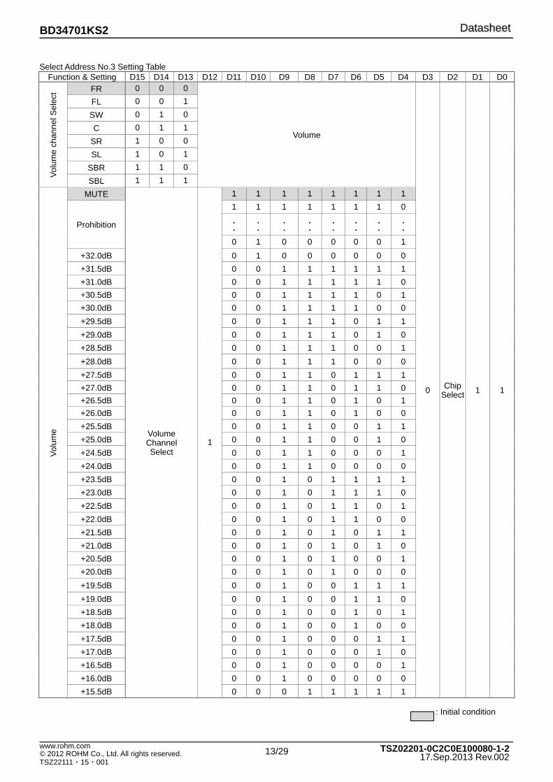
Select Address No.3 Setting Table
Function & Setting D15 D14 D13 D12 D11 D10 D9 D8 D7 D6 D5 D4 D3 D2 D1 D0
Volu
me
chan
nel S
elec
t FR 0 0 0
Volume
0 ChipSelect 1 1
FL 0 0 1 SW 0 1 0 C 0 1 1
SR 1 0 0 SL 1 0 1
SBR 1 1 0 SBL 1 1 1
Volu
me
MUTE
Volume Channel Select
1
1 1 1 1 1 1 1 1
Prohibition
1 1 1 1 1 1 1 0 . .
.
. . .
.
. . .
.
. . .
.
. 0 1 0 0 0 0 0 1
+32.0dB 0 1 0 0 0 0 0 0
+31.5dB 0 0 1 1 1 1 1 1
+31.0dB 0 0 1 1 1 1 1 0
+30.5dB 0 0 1 1 1 1 0 1
+30.0dB 0 0 1 1 1 1 0 0
+29.5dB 0 0 1 1 1 0 1 1
+29.0dB 0 0 1 1 1 0 1 0
+28.5dB 0 0 1 1 1 0 0 1
+28.0dB 0 0 1 1 1 0 0 0
+27.5dB 0 0 1 1 0 1 1 1
+27.0dB 0 0 1 1 0 1 1 0
+26.5dB 0 0 1 1 0 1 0 1
+26.0dB 0 0 1 1 0 1 0 0
+25.5dB 0 0 1 1 0 0 1 1
+25.0dB 0 0 1 1 0 0 1 0
+24.5dB 0 0 1 1 0 0 0 1
+24.0dB 0 0 1 1 0 0 0 0
+23.5dB 0 0 1 0 1 1 1 1
+23.0dB 0 0 1 0 1 1 1 0
+22.5dB 0 0 1 0 1 1 0 1
+22.0dB 0 0 1 0 1 1 0 0
+21.5dB 0 0 1 0 1 0 1 1
+21.0dB 0 0 1 0 1 0 1 0
+20.5dB 0 0 1 0 1 0 0 1
+20.0dB 0 0 1 0 1 0 0 0
+19.5dB 0 0 1 0 0 1 1 1
+19.0dB 0 0 1 0 0 1 1 0
+18.5dB 0 0 1 0 0 1 0 1
+18.0dB 0 0 1 0 0 1 0 0
+17.5dB 0 0 1 0 0 0 1 1
+17.0dB 0 0 1 0 0 0 1 0
+16.5dB 0 0 1 0 0 0 0 1
+16.0dB 0 0 1 0 0 0 0 0
+15.5dB 0 0 0 1 1 1 1 1
: Initial condition

14/29
DatasheetDatasheetBD34701KS2
© 2012 ROHM Co., Ltd. All rights reserved. www.rohm.com
TSZ22111・15・001
TSZ02201-0C2C0E100080-1-217.Sep.2013 Rev.002
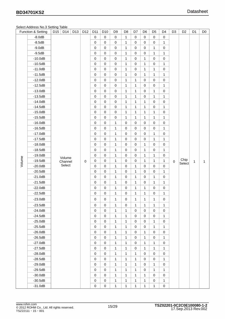
Select Address No.3 Setting Table
Function & Setting D15 D14 D13 D12 D11 D10 D9 D8 D7 D6 D5 D4 D3 D2 D1 D0
Volu
me
+15.0dB
Volume Channel Select
1
0 0 0 1 1 1 1 0
0 ChipSelect 1 1
+14.5dB 0 0 0 1 1 1 0 1
+14.0dB 0 0 0 1 1 1 0 0
+13.5dB 0 0 0 1 1 0 1 1
+13.0dB 0 0 0 1 1 0 1 0
+12.5dB 0 0 0 1 1 0 0 1
+12.0dB 0 0 0 1 1 0 0 0
+11.5dB 0 0 0 1 0 1 1 1
+11.0dB 0 0 0 1 0 1 1 0
+10.5dB 0 0 0 1 0 1 0 1
+10.0dB 0 0 0 1 0 1 0 0
+9.5dB 0 0 0 1 0 0 1 1
+9.0dB 0 0 0 1 0 0 1 0
+8.5dB 0 0 0 1 0 0 0 1
+8.0dB 0 0 0 1 0 0 0 0
+7.5dB 0 0 0 0 1 1 1 1
+7.0dB 0 0 0 0 1 1 1 0
+6.5dB 0 0 0 0 1 1 0 1
+6.0dB 0 0 0 0 1 1 0 0
+5.5dB 0 0 0 0 1 0 1 1
+5.0dB 0 0 0 0 1 0 1 0
+4.5dB 0 0 0 0 1 0 0 1
+4.0dB 0 0 0 0 1 0 0 0
+3.5dB 0 0 0 0 0 1 1 1
+3.0dB 0 0 0 0 0 1 1 0
+2.5dB 0 0 0 0 0 1 0 1
+2.0dB 0 0 0 0 0 1 0 0
+1.5dB 0 0 0 0 0 0 1 1
+1.0dB 0 0 0 0 0 0 1 0
+0.5dB 0 0 0 0 0 0 0 1
Prohibition 0 0 0 0 0 0 0 0
-0dB
0
0 0 0 0 0 0 0 0
-0.5dB 0 0 0 0 0 0 0 1
-1.0dB 0 0 0 0 0 0 1 0
-1.5dB 0 0 0 0 0 0 1 1
-2.0dB 0 0 0 0 0 1 0 0
-2.5dB 0 0 0 0 0 1 0 1
-3.0dB 0 0 0 0 0 1 1 0
-3.5dB 0 0 0 0 0 1 1 1
-4.0dB 0 0 0 0 1 0 0 0
-4.5dB 0 0 0 0 1 0 0 1
-5.0dB 0 0 0 0 1 0 1 0
-5.5dB 0 0 0 0 1 0 1 1
-6.0dB 0 0 0 0 1 1 0 0
-6.5dB 0 0 0 0 1 1 0 1
-7.0dB 0 0 0 0 1 1 1 0
-7.5dB 0 0 0 0 1 1 1 1
15/29
DatasheetDatasheetBD34701KS2
© 2012 ROHM Co., Ltd. All rights reserved. www.rohm.com
TSZ22111・15・001
TSZ02201-0C2C0E100080-1-217.Sep.2013 Rev.002
Select Address No.3 Setting Table
Function & Setting D15 D14 D13 D12 D11 D10 D9 D8 D7 D6 D5 D4 D3 D2 D1 D0
Volu
me
-8.0dB
Volume Channel Select
0
0 0 0 1 0 0 0 0
0 ChipSelect 1 1
-8.5dB 0 0 0 1 0 0 0 1
-9.0dB 0 0 0 1 0 0 1 0
-9.5dB 0 0 0 1 0 0 1 1
-10.0dB 0 0 0 1 0 1 0 0
-10.5dB 0 0 0 1 0 1 0 1
-11.0dB 0 0 0 1 0 1 1 0
-11.5dB 0 0 0 1 0 1 1 1
-12.0dB 0 0 0 1 1 0 0 0
-12.5dB 0 0 0 1 1 0 0 1
-13.0dB 0 0 0 1 1 0 1 0
-13.5dB 0 0 0 1 1 0 1 1
-14.0dB 0 0 0 1 1 1 0 0
-14.5dB 0 0 0 1 1 1 0 1
-15.0dB 0 0 0 1 1 1 1 0
-15.5dB 0 0 0 1 1 1 1 1
-16.0dB 0 0 1 0 0 0 0 0
-16.5dB 0 0 1 0 0 0 0 1
-17.0dB 0 0 1 0 0 0 1 0
-17.5dB 0 0 1 0 0 0 1 1
-18.0dB 0 0 1 0 0 1 0 0
-18.5dB 0 0 1 0 0 1 0 1
-19.0dB 0 0 1 0 0 1 1 0
-19.5dB 0 0 1 0 0 1 1 1
-20.0dB 0 0 1 0 1 0 0 0
-20.5dB 0 0 1 0 1 0 0 1
-21.0dB 0 0 1 0 1 0 1 0
-21.5dB 0 0 1 0 1 0 1 1
-22.0dB 0 0 1 0 1 1 0 0
-22.5dB 0 0 1 0 1 1 0 1
-23.0dB 0 0 1 0 1 1 1 0
-23.5dB 0 0 1 0 1 1 1 1
-24.0dB 0 0 1 1 0 0 0 0
-24.5dB 0 0 1 1 0 0 0 1
-25.0dB 0 0 1 1 0 0 1 0
-25.5dB 0 0 1 1 0 0 1 1
-26.0dB 0 0 1 1 0 1 0 0
-26.5dB 0 0 1 1 0 1 0 1
-27.0dB 0 0 1 1 0 1 1 0
-27.5dB 0 0 1 1 0 1 1 1
-28.0dB 0 0 1 1 1 0 0 0
-28.5dB 0 0 1 1 1 0 0 1
-29.0dB 0 0 1 1 1 0 1 0
-29.5dB 0 0 1 1 1 0 1 1
-30.0dB 0 0 1 1 1 1 0 0
-30.5dB 0 0 1 1 1 1 0 1
-31.0dB 0 0 1 1 1 1 1 0
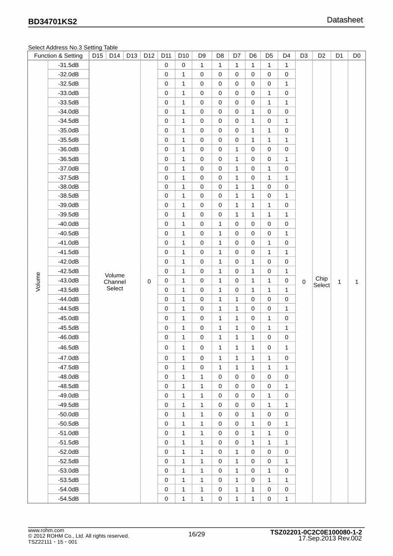
16/29
DatasheetDatasheetBD34701KS2
© 2012 ROHM Co., Ltd. All rights reserved. www.rohm.com
TSZ22111・15・001
TSZ02201-0C2C0E100080-1-217.Sep.2013 Rev.002
Select Address No.3 Setting Table
Function & Setting D15 D14 D13 D12 D11 D10 D9 D8 D7 D6 D5 D4 D3 D2 D1 D0
Volu
me
-31.5dB
Volume Channel Select
0
0 0 1 1 1 1 1 1
0 ChipSelect 1 1
-32.0dB 0 1 0 0 0 0 0 0
-32.5dB 0 1 0 0 0 0 0 1
-33.0dB 0 1 0 0 0 0 1 0
-33.5dB 0 1 0 0 0 0 1 1
-34.0dB 0 1 0 0 0 1 0 0
-34.5dB 0 1 0 0 0 1 0 1
-35.0dB 0 1 0 0 0 1 1 0
-35.5dB 0 1 0 0 0 1 1 1
-36.0dB 0 1 0 0 1 0 0 0
-36.5dB 0 1 0 0 1 0 0 1
-37.0dB 0 1 0 0 1 0 1 0
-37.5dB 0 1 0 0 1 0 1 1
-38.0dB 0 1 0 0 1 1 0 0
-38.5dB 0 1 0 0 1 1 0 1
-39.0dB 0 1 0 0 1 1 1 0
-39.5dB 0 1 0 0 1 1 1 1
-40.0dB 0 1 0 1 0 0 0 0
-40.5dB 0 1 0 1 0 0 0 1
-41.0dB 0 1 0 1 0 0 1 0
-41.5dB 0 1 0 1 0 0 1 1
-42.0dB 0 1 0 1 0 1 0 0
-42.5dB 0 1 0 1 0 1 0 1
-43.0dB 0 1 0 1 0 1 1 0
-43.5dB 0 1 0 1 0 1 1 1
-44.0dB 0 1 0 1 1 0 0 0
-44.5dB 0 1 0 1 1 0 0 1
-45.0dB 0 1 0 1 1 0 1 0
-45.5dB 0 1 0 1 1 0 1 1
-46.0dB 0 1 0 1 1 1 0 0
-46.5dB 0 1 0 1 1 1 0 1
-47.0dB 0 1 0 1 1 1 1 0
-47.5dB 0 1 0 1 1 1 1 1
-48.0dB 0 1 1 0 0 0 0 0
-48.5dB 0 1 1 0 0 0 0 1
-49.0dB 0 1 1 0 0 0 1 0
-49.5dB 0 1 1 0 0 0 1 1
-50.0dB 0 1 1 0 0 1 0 0
-50.5dB 0 1 1 0 0 1 0 1
-51.0dB 0 1 1 0 0 1 1 0
-51.5dB 0 1 1 0 0 1 1 1
-52.0dB 0 1 1 0 1 0 0 0
-52.5dB 0 1 1 0 1 0 0 1
-53.0dB 0 1 1 0 1 0 1 0
-53.5dB 0 1 1 0 1 0 1 1
-54.0dB 0 1 1 0 1 1 0 0
-54.5dB 0 1 1 0 1 1 0 1

17/29
DatasheetDatasheetBD34701KS2
© 2012 ROHM Co., Ltd. All rights reserved. www.rohm.com
TSZ22111・15・001
TSZ02201-0C2C0E100080-1-217.Sep.2013 Rev.002
Select Address No.3 Setting Table
Function & Setting D15 D14 D13 D12 D11 D10 D9 D8 D7 D6 D5 D4 D3 D2 D1 D0
Volu
me
-55.0dB
Volume Channel Select
0
0 1 1 0 1 1 1 0
0 ChipSelect 1 1
-55.5dB 0 1 1 0 1 1 1 1
-56.0dB 0 1 1 1 0 0 0 0
-56.5dB 0 1 1 1 0 0 0 1
-57.0dB 0 1 1 1 0 0 1 0
-57.5dB 0 1 1 1 0 0 1 1
-58.0dB 0 1 1 1 0 1 0 0
-58.5dB 0 1 1 1 0 1 0 1
-59.0dB 0 1 1 1 0 1 1 0
-59.5dB 0 1 1 1 0 1 1 1
-60.0dB 0 1 1 1 1 0 0 0
-60.5dB 0 1 1 1 1 0 0 1
-61.0dB 0 1 1 1 1 0 1 0
-61.5dB 0 1 1 1 1 0 1 1
-62.0dB 0 1 1 1 1 1 0 0
-62.5dB 0 1 1 1 1 1 0 1
-63.0dB 0 1 1 1 1 1 1 0
-63.5dB 0 1 1 1 1 1 1 1
-64.0dB 1 0 0 0 0 0 0 0
-64.5dB 1 0 0 0 0 0 0 1
-65.0dB 1 0 0 0 0 0 1 0
-65.5dB 1 0 0 0 0 0 1 1
-66.0dB 1 0 0 0 0 1 0 0
-66.5dB 1 0 0 0 0 1 0 1
-67.0dB 1 0 0 0 0 1 1 0
-67.5dB 1 0 0 0 0 1 1 1
-68.0dB 1 0 0 0 1 0 0 0
-68.5dB 1 0 0 0 1 0 0 1
-69.0dB 1 0 0 0 1 0 1 0
-69.5dB 1 0 0 0 1 0 1 1
-70.0dB 1 0 0 0 1 1 0 0
-70.5dB 1 0 0 0 1 1 0 1
-71.0dB 1 0 0 0 1 1 1 0
-71.5dB 1 0 0 0 1 1 1 1
-72.0dB 1 0 0 1 0 0 0 0
-72.5dB 1 0 0 1 0 0 0 1
-73.0dB 1 0 0 1 0 0 1 0
-73.5dB 1 0 0 1 0 0 1 1
-74.0dB 1 0 0 1 0 1 0 0
-74.5dB 1 0 0 1 0 1 0 1
-75.0dB 1 0 0 1 0 1 1 0
-75.5dB 1 0 0 1 0 1 1 1
-76.0dB 1 0 0 1 1 0 0 0
-76.5dB 1 0 0 1 1 0 0 1
-77.0dB 1 0 0 1 1 0 1 0
-77.5dB 1 0 0 1 1 0 1 1
-78.0dB 1 0 0 1 1 1 0 0

18/29
DatasheetDatasheetBD34701KS2
© 2012 ROHM Co., Ltd. All rights reserved. www.rohm.com
TSZ22111・15・001
TSZ02201-0C2C0E100080-1-217.Sep.2013 Rev.002
Select Address No.3 Setting Table
Function & Setting D15 D14 D13 D12 D11 D10 D9 D8 D7 D6 D5 D4 D3 D2 D1 D0
Volu
me
-78.5dB
Volume Channel Select
0
1 0 0 1 1 1 0 1
0 ChipSelect 1 1
-79.0dB 1 0 0 1 1 1 1 0
-79.5dB 1 0 0 1 1 1 1 1
-80.0dB 1 0 1 0 0 0 0 0
-80.5dB 1 0 1 0 0 0 0 1
-81.0dB 1 0 1 0 0 0 1 0
-81.5dB 1 0 1 0 0 0 1 1
-82.0dB 1 0 1 0 0 1 0 0
-82.5dB 1 0 1 0 0 1 0 1
-83.0dB 1 0 1 0 0 1 1 0
-83.5dB 1 0 1 0 0 1 1 1
-84.0dB 1 0 1 0 1 0 0 0
-84.5dB 1 0 1 0 1 0 0 1
-85.0dB 1 0 1 0 1 0 1 0
-85.5dB 1 0 1 0 1 0 1 1
-86.0dB 1 0 1 0 1 1 0 0
-86.5dB 1 0 1 0 1 1 0 1
-87.0dB 1 0 1 0 1 1 1 0
-87.5dB 1 0 1 0 1 1 1 1
-88.0dB 1 0 1 1 0 0 0 0
-88.5dB 1 0 1 1 0 0 0 1
-89.0dB 1 0 1 1 0 0 1 0
-89.5dB 1 0 1 1 0 0 1 1
-90.0dB 1 0 1 1 0 1 0 0
-90.5dB 1 0 1 1 0 1 0 1
-91.0dB 1 0 1 1 0 1 1 0
-91.5dB 1 0 1 1 0 1 1 1
-92.0dB 1 0 1 1 1 0 0 0
-92.5dB 1 0 1 1 1 0 0 1
-93.0dB 1 0 1 1 1 0 1 0
-93.5dB 1 0 1 1 1 0 1 1
-94.0dB 1 0 1 1 1 1 0 0
-94.5dB 1 0 1 1 1 1 0 1
-95.0dB 1 0 1 1 1 1 1 0
Prohibition
1 0 1 1 1 1 1 1
.
. . .
.
. . .
.
. . .
.
. . .
1 1 1 1 1 1 1 1
19/29
DatasheetDatasheetBD34701KS2
© 2012 ROHM Co., Ltd. All rights reserved. www.rohm.com
TSZ22111・15・001
TSZ02201-0C2C0E100080-1-217.Sep.2013 Rev.002
Select Address No.7 Setting TableFunction & Setting D15 D14 D13 D12 D11 D10 D9 D8 D7 D6 D5 D4 D3 D2 D1 D0
A→
B
switc
hing
-tim
e
11msec 0 0 0
B→A switching-time
Baseclock
0 0
SystemReset
0 0 1 ChipSelect 1 1
5msec 0 0 1
7msec 0 1 0
14msec 0 1 1
3msec 1 0 0
2msec 1 0 1
Prohibition 1 1 0
1 1 1
B→
A
switc
hing
-tim
e
11msec
A→B switching-time
0 0 0
5msec 0 0 1
7msec 0 1 0
14msec 0 1 1
3msec 1 0 0
2msec 1 0 1
Prohibition 1 1 0
1 1 1
Bas
e cl
ock x1
B→A switching-time
0
×1/2 1
Sys
tem
R
eset
Normal Baseclock
0
Reset 1
: Initial condition
20/29
DatasheetDatasheetBD34701KS2
© 2012 ROHM Co., Ltd. All rights reserved. www.rohm.com
TSZ22111・15・001
TSZ02201-0C2C0E100080-1-217.Sep.2013 Rev.002
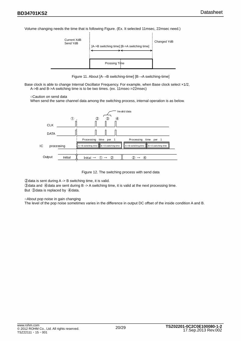
Volume changing needs the time that is following Figure. (Ex. It selected 11msec, 22msec need.)
Figure 11. About [A→B switching-time] [B→A switching-time]
Base clock is able to change Internal Oscillator Frequency. For example, when Base clock select ×1/2, A->B and B->A switching time is to be two times. (ex. 11msec->22msec)
Caution on send data When send the same channel data among the switching process, internal operation is as below.
Figure 12. The switching process with send data
②data is sent during A -> B switching time, it is valid. ③data and ④data are sent during B -> A switching time, it is valid at the next processing time. But ③data is replaced by ④data. About pop noise in gain changing The level of the pop noise sometimes varies in the difference in output DC offset of the inside condition A and B.
Prossing Time
[A->B switching time] [B->A switching time]
Current XdB Send YdB
Changed YdB
CLK
DATA
IC processing
Output Initial → ① → ② ② → ④
④ ③ ② ①
Invalid data
Initial
Processing time per 1 Processing time per 1
A->B switching time B->A switching t ime A->B switching time B->A switching time

21/29
DatasheetDatasheetBD34701KS2
© 2012 ROHM Co., Ltd. All rights reserved. www.rohm.com
TSZ22111・15・001
TSZ02201-0C2C0E100080-1-217.Sep.2013 Rev.002
Logic
FR Volume
FL Volume
SW Volume
C Volume
SRVolume
SL Volume
SBR Volume
SBLVolume
Modeselector
Rec
ADC
26
25
24
23
22
21
1 2 3 4 5 6 7 8 9 10 11 12 13
20
19
18
17
16
15
14
GS
MG
SM
GS
MG
SM
30 29 28 2734 33 32 3138 37 36 3539
GSMGSMGSMGSMGSMGSMGSMGSMGSMGSMGSMGSM
40
41
42
43
44
45
46
47
48
49
50
51
52
GS
MG
SM
GS
MG
SM
GS
MG
SM
GS
MG
SM
Main
OUTSBR OUTSBLOUTSR OUTSLOUTSW OUTCCLDGND DA
47 µ 0.1µVEE
47µ 0.1 µOUTFR OUTFL
SUBR
SUBL
RECR
RECL
GND
GND
GND
GND
INL8
INR8
INL7
INR7
GND
INL6INR6INL5INR5INL4INR4INL3INR3INL2INR2INL1INR1GND
SBLIN
SBRIN
SLIN
SRIN
CIN
SWIN
FLIN
FRIN
GND
GND
ADCR
ADCL
CHP
VCC
Modeselector
Modeselector
Modeselector
Sub
MULTIINPUT
STEREOINPUT
INR9
INL12
INR12
INL11
INR11
INL10
INR10
INL9
Application Circuit Diagram
Figure 13. Application Circuit Diagram
Notes on wiring ① GND shall be wired from reference point and thicken. ② Wiring pattern of CL and DA shall be away from that of analog unit and cross-talk shall not be acceptable. ③ Lines of CL and DA of shall not be parallel if possible. The lines shall be shielded, if they are adjacent to each other. ④ Please pay attention the wiring pattern of the input terminal of the input selector to the cross talk. Recommend that
wiring period is shielded. ⑤ Please connect the decoupling capacitor of a power supply in the shortest distance as much as possible to VCC and
GND, VEE.

22/29
DatasheetDatasheetBD34701KS2
© 2012 ROHM Co., Ltd. All rights reserved. www.rohm.com
TSZ22111・15・001
TSZ02201-0C2C0E100080-1-217.Sep.2013 Rev.002
Power Dissipation
About the thermal design by the IC Characteristics of an IC have a great deal to do with the temperature at which it is used, and exceeding absolute maximum ratings may degrade and destroy elements. Careful consideration must be given to the heat of the IC from the two standpoints of immediate damage and long-term reliability of operation.
Figure 14. Temperature Derating Curve
Note) Value are actual measurements and are not guaranteed.
Power dissipation values vary according to the board on which the IC is mounted.
Reference data
SQFP-T52
2.0
1.0
0.0
0 25 50 75 100 125 150
Ambient Temperature Ta(°C)
Pow
er D
issi
patio
n P
d(W
)
1.30W
θja = 76.9°C/W
85
Measurement condition: ROHM Standard board board Size:70×70×1.6() material:A FR4 grass epoxy board
(3% or less of copper foil area)
23/29
DatasheetDatasheetBD34701KS2
© 2012 ROHM Co., Ltd. All rights reserved. www.rohm.com
TSZ22111・15・001
TSZ02201-0C2C0E100080-1-217.Sep.2013 Rev.002
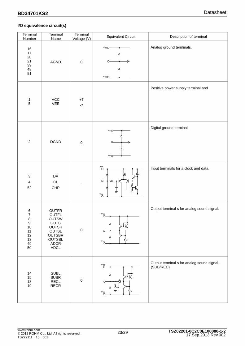
I/O equivalence circuit(s)
Terminal Number
Terminal Name
Terminal Voltage (V) Equivalent Circuit Description of terminal
16 17 20 21 39 48 51
AGND 0
Analog ground terminals.
1 5
VCC VEE
+7 -7
Positive power supply terminal and
2 DGND 0
Digital ground terminal.
3 4
52
DA CL
CHP -
Input terminals for a clock and data.
6 7 8 9
10 11 12 13 49 50
OUTFR OUTFL OUTSW OUTC
OUTSR OUTSL
OUTSBR OUTSBL
ADCR ADCL
0
Output terminal s for analog sound signal.
14 15 18 19
SUBL SUBR RECL RECR
0
Output terminal s for analog sound signal. (SUB/REC)
Vee
Vcc
Vcc
Vee
Vee
Vcc
Vcc
Vee
47k
Vcc
Vee

24/29
DatasheetDatasheetBD34701KS2
© 2012 ROHM Co., Ltd. All rights reserved. www.rohm.com
TSZ22111・15・001
TSZ02201-0C2C0E100080-1-217.Sep.2013 Rev.002
Terminal Number
Terminal Name
Terminal Voltage (V) Equivalent Circuit Description of terminal
22 23 24 25 27 28 29 30 31 32 33 34 35 36 37 38
INL8 INR8 INL7 INR7 INL6 INR6 INL5 INR5 INL4 INR4 INL3 INR3 INL2 INR2 INL1 INR1
0
Input terminals for stereo sound signal. Input impedance is 47kΩ(Typ.).
40 41 42 43 44 45 46 47
SBLIN SBRIN SLIN SRIN CIN
SWIN FLIN FRIN
0
Input terminals for an analog multi sound signal. Input impedance is 47kΩ(Typ.).
Vcc
Vee
47k
Vcc
Vee
47k
25/29
DatasheetDatasheetBD34701KS2
© 2012 ROHM Co., Ltd. All rights reserved. www.rohm.com
TSZ22111・15・001
TSZ02201-0C2C0E100080-1-217.Sep.2013 Rev.002
Operational Notes
1. Reverse Connection of Power Supply Connecting the power supply in reverse polarity can damage the IC. Take precautions against reverse polarity when connecting the power supply, such as mounting an external diode between the power supply and the IC’s power supply terminals.
2. Power Supply Lines Design the PCB layout pattern to provide low impedance supply lines. Separate the ground and supply lines of the digital and analog blocks to prevent noise in the ground and supply lines of the digital block from affecting the analog block. Furthermore, connect a capacitor to ground at all power supply pins. Consider the effect of temperature and aging on the capacitance value when using electrolytic capacitors.
3. Vee Voltage Ensure that no pins are at a voltage below that of the VEE pin at any time, even during transient condition.
4. Ground Wiring Pattern
GND pins which are digital ground(2pin) and analog ground(16,17,20,21,26,39,48,51pin) are not connected inside LSI. These ground pins traces should be routed separately but connected to a single ground at the reference point of the application board. Also ensure that the ground traces of external components do not cause variations on the ground voltage. The ground lines must be as short and thick as possible to reduce line impedance.
5. Thermal Consideration
Should by any chance the power dissipation rating be exceeded the rise in temperature of the chip may result in deterioration of the properties of the chip. The absolute maximum rating of the Pd stated in this specification is when the IC is mounted on a 70mm x 70mm x 1.6mm glass epoxy board. In case of exceeding this absolute maximum rating, increase the board size and copper area to prevent exceeding the Pd rating.
6. Recommended Operating Conditions
These conditions represent a range within which the expected characteristics of the IC can be approximately obtained. The electrical characteristics are guaranteed under the conditions of each parameter.
7. Rush Current
When power is first supplied to the IC, it is possible that the internal logic may be unstable and inrush current may flow instantaneously due to the internal powering sequence and delays, especially if the IC has more than one power supply. Therefore, give special consideration to power coupling capacitance, power wiring, width of ground wiring, and routing of connections.
8. Operation Under Strong Electromagnetic Field
Operating the IC in the presence of a strong electromagnetic field may cause the IC to malfunction.
9. Testing on Application Boards When testing the IC on an application board, connecting a capacitor directly to IC pin may subject the IC to stress. Always discharge capacitors completely after each process or step. The IC’s power supply should always be turned off completely before connecting or removing it from the test setup during the inspection process. To prevent damage from static discharge, ground the IC during assembly and use similar precautions during transport and storage.
10. Inter-pin Short and Mounting Errors Ensure that the direction and position are correct when mounting the IC on the PCB. Incorrect mounting may result in damaging the IC. Avoid nearby pins being shorted to each other especially to ground, power supply and output pin. Inter-pin shorts could be due to many reasons such as metal particles, water droplets (in very humid environment) and unintentional solder bridge deposited in between pins during assembly to name a few.
11. Unused Input Terminals
Because the input impedance of the terminal becomes 47kΩ when the signal input terminal makes a terminal open, the plunge noise from outside sometimes becomes a problem. Please connect the no using input pin to GND. And please open the no using output pin.

26/29
DatasheetDatasheetBD34701KS2
© 2012 ROHM Co., Ltd. All rights reserved. www.rohm.com
TSZ22111・15・001
TSZ02201-0C2C0E100080-1-217.Sep.2013 Rev.002
Operational Notes – continued 1
12. Regarding the Input Pin of the IC This monolithic IC contains P+ isolation and P substrate layers between adjacent elements in order to keep them isolated. P-N junctions are formed at the intersection of the P layers with the N layers of other elements, creating a parasitic diode or transistor. For example (refer to figure below):
When Vee > Pin A and Vee > Pin B, the P-N junction operates as a parasitic diode. When Vee > Pin B, the P-N junction operates as a parasitic transistor.
Parasitic diodes inevitably occur in the structure of the IC. The operation of parasitic diodes can result in mutual interference among circuits, operational faults, or physical damage. Therefore, conditions that cause these diodes to operate, such as applying a voltage lower than the Vee voltage to an input pin (and thus to the P substrate) should be avoided.
Figure 15. Example of monolithic IC structure
13. Ceramic Capacitor When using a ceramic capacitor, determine the dielectric constant considering the change of capacitance with temperature and the decrease in nominal capacitance due to DC bias and others.
14. About power ON/OFF
1. At power ON/OFF, a shock sound will be generated and, therefore, use MUTE on the set. 2. When turning on power supplies, Vee and Vcc should be powered on simultaneously or Vee first; then followed by Vcc. If the Vcc side is started up first, an excessive current may pass Vcc through Vee.
15. About function switching
When switching Input Selector, Mode selector or Input Gain, use MUTE on Volume.
16. Volume gain switching In case of the boost of the volume when changing to the high gain which exceeds +20dB especially, the switching shock noise sometimes becomes big. In this case, we recommend changing every 1 dB step without changing a gain at once. Also, the shock noise sometimes can reduce by making micro-step volume switching time long, too.
N N P+ PN N P +
P Substrate
Vee
N P+
N NP+N P
P Substrate
Vee Vee
Parasitic Elements
Pin A
Pin A
Pin B Pin B
B C
EParasitic Elements
VeeParasitic Elements
C B
E
Transistor ( NPN) Resistor
N Regionclose - by
ParasiticElements

27/29
DatasheetDatasheetBD34701KS2
© 2012 ROHM Co., Ltd. All rights reserved. www.rohm.com
TSZ22111・15・001
TSZ02201-0C2C0E100080-1-217.Sep.2013 Rev.002
Operational Notes – continued 2
17. Output load characteristic The usages of load for output are below (reference). Please use the load more than 10 kΩ(TYP).
Output terminal Terminal
No. Terminal Name
Terminal No.
Terminal Name
Terminal No.
Terminal Name
Terminal No.
Terminal Name
6 OUTFR 10 OUTSR 14 SUBL 49 ADCR 7 OUTFL 11 OUTSL 15 SUBR 50 ADCL 8 OUTSW 12 OUTSBR 18 RECL - - 9 OUTC 13 OUTSBL 19 RECR - -
Figure 16. Output load characteristic at Vcc=+7V, Vee=-7V(Reference)
Ordering Information
B D 3 4 7 0 1 K S 2 -
Part Number Package KS2: SQFP-T52
Packaging and forming specification none: Tray E2: Embossed tape and reel
Marking Diagram(TOP VIEW)
SQFP-T52 (TOP VIEW) Part Number Marking
LOT Number
1PIN MARK
B D 3 4 7 0 1 K S 2
0
0.5
1
1.5
2
2.5
3
3.5
4
4.5
5
100 1000 10000 100000
Load Resistance Ω
VO
,max V
rms
Vcc=+7V Vee=-7V THD+n=1% BW=400~30kHz
28/29
DatasheetDatasheetBD34701KS2
© 2012 ROHM Co., Ltd. All rights reserved. www.rohm.com
TSZ22111・15・001
TSZ02201-0C2C0E100080-1-217.Sep.2013 Rev.002
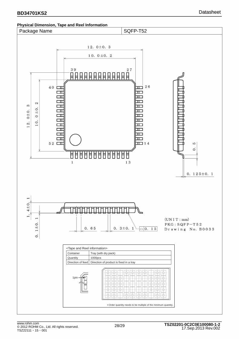
Physical Dimension, Tape and Reel Information Package Name SQFP-T52
∗ Order quantity needs to be multiple of the minimum quantity.
<Tape and Reel information>
Tray (with dry pack)Container
Quantity
Direction of feed
1000pcs
Direction of product is fixed in a tray
1pin

29/29
DatasheetDatasheetBD34701KS2
© 2012 ROHM Co., Ltd. All rights reserved. www.rohm.com
TSZ22111・15・001
TSZ02201-0C2C0E100080-1-217.Sep.2013 Rev.002
Revision History Date Revision Changes
02.Sep.2013 001 New Release 17.Sep.2003 002 P27. Delete “M” of “SQFP-T52M” in Marking Diagram.
DatasheetDatasheet
Notice - GE Rev.002© 2014 ROHM Co., Ltd. All rights reserved.
Notice Precaution on using ROHM Products
1. Our Products are designed and manufactured for application in ordinary electronic equipments (such as AV equipment, OA equipment, telecommunication equipment, home electronic appliances, amusement equipment, etc.). If you intend to use our Products in devices requiring extremely high reliability (such as medical equipment (Note 1), transport equipment, traffic equipment, aircraft/spacecraft, nuclear power controllers, fuel controllers, car equipment including car accessories, safety devices, etc.) and whose malfunction or failure may cause loss of human life, bodily injury or serious damage to property (“Specific Applications”), please consult with the ROHM sales representative in advance. Unless otherwise agreed in writing by ROHM in advance, ROHM shall not be in any way responsible or liable for any damages, expenses or losses incurred by you or third parties arising from the use of any ROHM’s Products for Specific Applications.
(Note1) Medical Equipment Classification of the Specific Applications JAPAN USA EU CHINA
CLASSⅢ CLASSⅢ
CLASSⅡb CLASSⅢ
CLASSⅣ CLASSⅢ
2. ROHM designs and manufactures its Products subject to strict quality control system. However, semiconductor
products can fail or malfunction at a certain rate. Please be sure to implement, at your own responsibilities, adequate safety measures including but not limited to fail-safe design against the physical injury, damage to any property, which a failure or malfunction of our Products may cause. The following are examples of safety measures:
[a] Installation of protection circuits or other protective devices to improve system safety [b] Installation of redundant circuits to reduce the impact of single or multiple circuit failure
3. Our Products are designed and manufactured for use under standard conditions and not under any special or extraordinary environments or conditions, as exemplified below. Accordingly, ROHM shall not be in any way responsible or liable for any damages, expenses or losses arising from the use of any ROHM’s Products under any special or extraordinary environments or conditions. If you intend to use our Products under any special or extraordinary environments or conditions (as exemplified below), your independent verification and confirmation of product performance, reliability, etc, prior to use, must be necessary:
[a] Use of our Products in any types of liquid, including water, oils, chemicals, and organic solvents [b] Use of our Products outdoors or in places where the Products are exposed to direct sunlight or dust [c] Use of our Products in places where the Products are exposed to sea wind or corrosive gases, including Cl2,
H2S, NH3, SO2, and NO2
[d] Use of our Products in places where the Products are exposed to static electricity or electromagnetic waves [e] Use of our Products in proximity to heat-producing components, plastic cords, or other flammable items [f] Sealing or coating our Products with resin or other coating materials [g] Use of our Products without cleaning residue of flux (even if you use no-clean type fluxes, cleaning residue of
flux is recommended); or Washing our Products by using water or water-soluble cleaning agents for cleaning residue after soldering
[h] Use of the Products in places subject to dew condensation
4. The Products are not subject to radiation-proof design. 5. Please verify and confirm characteristics of the final or mounted products in using the Products. 6. In particular, if a transient load (a large amount of load applied in a short period of time, such as pulse. is applied,
confirmation of performance characteristics after on-board mounting is strongly recommended. Avoid applying power exceeding normal rated power; exceeding the power rating under steady-state loading condition may negatively affect product performance and reliability.
7. De-rate Power Dissipation (Pd) depending on Ambient temperature (Ta). When used in sealed area, confirm the actual
ambient temperature. 8. Confirm that operation temperature is within the specified range described in the product specification. 9. ROHM shall not be in any way responsible or liable for failure induced under deviant condition from what is defined in
this document.
Precaution for Mounting / Circuit board design 1. When a highly active halogenous (chlorine, bromine, etc.) flux is used, the residue of flux may negatively affect product
performance and reliability. 2. In principle, the reflow soldering method must be used; if flow soldering method is preferred, please consult with the
ROHM representative in advance. For details, please refer to ROHM Mounting specification

DatasheetDatasheet
Notice - GE Rev.002© 2014 ROHM Co., Ltd. All rights reserved.
Precautions Regarding Application Examples and External Circuits 1. If change is made to the constant of an external circuit, please allow a sufficient margin considering variations of the
characteristics of the Products and external components, including transient characteristics, as well as static characteristics.
2. You agree that application notes, reference designs, and associated data and information contained in this document
are presented only as guidance for Products use. Therefore, in case you use such information, you are solely responsible for it and you must exercise your own independent verification and judgment in the use of such information contained in this document. ROHM shall not be in any way responsible or liable for any damages, expenses or losses incurred by you or third parties arising from the use of such information.
Precaution for Electrostatic
This Product is electrostatic sensitive product, which may be damaged due to electrostatic discharge. Please take proper caution in your manufacturing process and storage so that voltage exceeding the Products maximum rating will not be applied to Products. Please take special care under dry condition (e.g. Grounding of human body / equipment / solder iron, isolation from charged objects, setting of Ionizer, friction prevention and temperature / humidity control).
Precaution for Storage / Transportation 1. Product performance and soldered connections may deteriorate if the Products are stored in the places where:
[a] the Products are exposed to sea winds or corrosive gases, including Cl2, H2S, NH3, SO2, and NO2 [b] the temperature or humidity exceeds those recommended by ROHM [c] the Products are exposed to direct sunshine or condensation [d] the Products are exposed to high Electrostatic
2. Even under ROHM recommended storage condition, solderability of products out of recommended storage time period may be degraded. It is strongly recommended to confirm solderability before using Products of which storage time is exceeding the recommended storage time period.
3. Store / transport cartons in the correct direction, which is indicated on a carton with a symbol. Otherwise bent leads
may occur due to excessive stress applied when dropping of a carton. 4. Use Products within the specified time after opening a humidity barrier bag. Baking is required before using Products of
which storage time is exceeding the recommended storage time period.
Precaution for Product Label QR code printed on ROHM Products label is for ROHM’s internal use only.
Precaution for Disposition When disposing Products please dispose them properly using an authorized industry waste company.
Precaution for Foreign Exchange and Foreign Trade act Since our Products might fall under controlled goods prescribed by the applicable foreign exchange and foreign trade act, please consult with ROHM representative in case of export.
Precaution Regarding Intellectual Property Rights 1. All information and data including but not limited to application example contained in this document is for reference
only. ROHM does not warrant that foregoing information or data will not infringe any intellectual property rights or any other rights of any third party regarding such information or data. ROHM shall not be in any way responsible or liable for infringement of any intellectual property rights or other damages arising from use of such information or data.:
2. No license, expressly or implied, is granted hereby under any intellectual property rights or other rights of ROHM or any
third parties with respect to the information contained in this document.
Other Precaution 1. This document may not be reprinted or reproduced, in whole or in part, without prior written consent of ROHM. 2. The Products may not be disassembled, converted, modified, reproduced or otherwise changed without prior written
consent of ROHM. 3. In no event shall you use in any way whatsoever the Products and the related technical information contained in the
Products or this document for any military purposes, including but not limited to, the development of mass-destruction weapons.
4. The proper names of companies or products described in this document are trademarks or registered trademarks of
ROHM, its affiliated companies or third parties.
DatasheetDatasheet
Notice – WE Rev.001© 2014 ROHM Co., Ltd. All rights reserved.
General Precaution 1. Before you use our Pro ducts, you are requested to care fully read this document and fully understand its contents.
ROHM shall n ot be in an y way responsible or liabl e for fa ilure, malfunction or acci dent arising from the use of a ny ROHM’s Products against warning, caution or note contained in this document.
2. All information contained in this docume nt is current as of the issuing date and subj ect to change without any prior
notice. Before purchasing or using ROHM’s Products, please confirm the la test information with a ROHM sale s representative.
3. The information contained in this doc ument is provi ded on an “as is” basis and ROHM does not warrant that all
information contained in this document is accurate an d/or error-free. ROHM shall not be in an y way responsible or liable for any damages, expenses or losses incurred by you or third parties resulting from inaccuracy or errors of or concerning such information.