space-confined growth of high-quality csbi i lead- free
TRANSCRIPT

mater.scichina.com link.springer.com Published online 9 October 2020 | https://doi.org/10.1007/s40843-020-1447-3Sci China Mater 2021, 64(2): 393–399
Space-confined growth of high-quality CsBi3I10 lead-free perovskite film for near-infrared photodetectorswith high sensitivity and stabilityRonghuan Liu, Hai Zhou*, Rui Wang, Dingjun Wu, Xiyan Pan, Guangdong Pan and Hao Wang*
ABSTRACT As a lead-free perovskite, CsBi3I10 has attractedsignificant attention because of its high thermal tolerance andlong electron diffusion length. Solution-processed high-performance CsBi3I10 perovskite devices, however, are hin-dered by the formation of a two-dimensional structure, whichresults in an extremely high surface roughness and manypinholes. In this paper, we reported a space-confined growth(SCG) method using a single-layer polystyrene (PS) spheretemplate to obtain high-smoothness, high-crystallinity, anddense CsBi3I10 perovskite films. Compared with traditionallyspin-coated CsBi3I10 photodetectors (PDs), the metal-semiconductor-metal PDs made by SCG showed a higherphotocurrent, a lower dark current, and a bigger on/off ratio.In addition, the photocurrent of our unencapsulated CsBi3I10perovskite PDs was not attenuated under long-time illumi-nation. In addition, when the device was stored in air for 30 d,its performance also showed no degradation, demonstratingultra-high stability. Furthermore, the synthesis was free ofantisolvents, such as chlorobenzene and toluene, which isbeneficial for the environmentally friendly assembly of thedevices. Our strategy opens up a new way to prepare high-quality lead-free perovskite, which may be useful for applica-tions in light-emitting diodes and solar cells.
Keywords: photodetectors, perovskite, space-confined growth,lead-free
INTRODUCTIONPhotodetectors (PDs) have attracted significant attentionbecause of their wide applications in various fields, suchas the military and national economy [1–3]. Today, leadhalide perovskite materials have been widely studied inPDs because of their high light absorption coefficient,long carrier diffusion length, and low defect state density
[4–9]. The detectivity of perovskite PDs has reached1015 Jones [6]. Although lead halide perovskite PDs havemade excellent progress, commercial application of thesedevices has been limited by the presence of toxic lead[10]. Therefore, research on leadless or lead-free per-ovskite materials has become a hot topic [11–14], parti-cularly on the exploration of lead-free perovskites, whichexhibit the same merits as those in the perovskite familywhile still exhibiting high device performance and stabi-lity.In recent years, excellent advances have been reported
by replacing lead with tin for leadless or lead-free per-ovskite optoelectronic devices [15–18]. Waleed et al. [16]reported a CH3NH3SnI3 (CH3NH3=MA, MASnI3) nano-wire array PD with a responsivity that reached 0.47 A W−1
and detectivity of 8.8 × 10¹⁰ Jones. Zhu et al. [18] pre-pared a MA0.9Rb0.1Sn0.65Pb0.35I3 detector with a lineardynamic range (LDR) reaching 110 and an 3-dB cut-offfrequency of 1 MHz. Other reports, however, have in-dicated more serious environmental implications follow-ing the use of tin compared with lead. In addition, theeasy oxidation of Sn2+ to Sn4+ often results in the sig-nificant instability of Sn-based perovskite devices [19].Germanium has been suggested as another lead replace-ment metal; however, this rare germanium is expensiveand requires additional refinement [20]. Bismuth, anontoxic metal that has similar properties to lead, is agood choice for Bi-based perovskite because of its longelectron diffusion length (>1.9 µm) [21]. Therefore, Bi isexpected to replace Sn as a next-generation, en-vironmentally friendly perovskite material. In 2015, Parket al. [22] reported the application of Cs3Bi2I9 perovskitematerial in a solar cell with an efficiency of 1.09%. Jo-hansson et al. [20] synthesized black CsBi3I10 perovskite
Hubei Key Laboratory of Ferro & Piezoelectric Materials and Devices, Faculty of Physics & Electronic Science, Hubei University, Wuhan 430062,China* Corresponding authors (emails: [email protected] (Zhou H); [email protected] (Wang H))
SCIENCE CHINA Materials. . . . . . . . . . . . . . . . . . . . . . . . . . . . . . . .ARTICLES
February 2021 | Vol. 64 No.2 393© Science China Press and Springer-Verlag GmbH Germany, part of Springer Nature 2020
by adding BiI3 in the Cs3Bi2I9, lowering its band gap from2.03 to 1.77 eV, which widened the light absorption rangeof the material and made it more suitable for the pre-paration of solar cells. The Bi-based perovskite more ea-sily forms a two-dimensional structure, and its surfaceroughness is extremely large with lots of pinholes, whichseverely limits the application of the CsBi3I10 perovskite inoptoelectronic devices.In this study, we obtained high-smoothness, high-
crystallinity, and dense black CsBi3I10 perovskite thinfilms using space-confined growth (SCG) with a single-layer polystyrene (PS) sphere template. The performanceof the metal-semiconductor-metal (MSM) PDs usingSCG was better than that of the traditionally spin-coatedCsBi3I10 PDs. Additionally, the photocurrent of our un-encapsulated CsBi3I10 perovskite PDs was not attenuatedunder long-term illumination. In addition, when the de-vice was stored in air for 30 d, its performance showed nodegradation, indicating its ultra-high stability. Further-more, this work did not require the use of toxic anti-solvents, such as chlorobenzene and toluene, suggestingits benefit for the environmentally friendly assembly ofthe devices.
EXPERIMENTAL SECTION
Traditionally spin-coated CsBi3I10 filmWe prepared the precursors of perovskite by dissolving0.2598 g CsI (99.999%) and 1.769 g BiI3 (99.999%) in1 mL dimethyl sulfoxide (99.9%) and keeping the mixturein the oven at 70°C for 24 h. Before use, we filtered theprecursor with a 0.22-μm filter. Then, we added 80 μL ofperovskite precursor solution to the substrate, which wasrotated at 3,000 rpm for 30 s. The samples were thenannealed at 100°C for 20 min.
SCG CsBi3I10 filmThe CsBi3I10 precursor solution was spun on the substratewith a single-layer PS sphere (details are presented in ourprevious work [23]). The substrate was rotated at3,000 rpm for 30 s and no other antisolvents were used.The samples were then annealed at 100°C for 20 min.
Device fabricationA 70-nm Au electrode (Fig. S1) with a finger spacing of100 μm was evaporated on the CsBi3I10 film to form anAu/CsBi3I10/Au MSM PD.
CharacterizationWe took high-resolution scanning electron microscopy
(SEM) images using field emission scanning electronmicroscopy (FESEM, JEOL, JSM-6700F), obtained X-raydiffraction (XRD) patterns using a D8 FOCUS X-raydiffractometer, and measured the absorption spectrausing an ultraviolet-visible spectrophotometer. We mea-sured the current-voltage (I–V) and current-time (I–t)curves using an Agilent B1500A electrometer. We used a473-nm laser (50 mW) as the light source and calibratedits optical power by a standard Si diode.
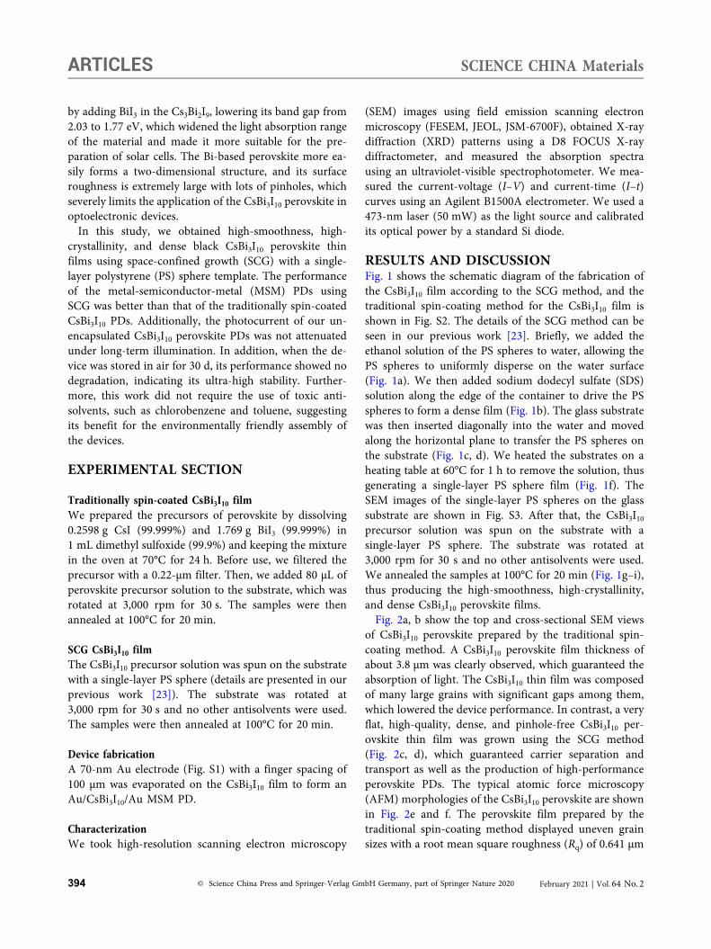
RESULTS AND DISCUSSIONFig. 1 shows the schematic diagram of the fabrication ofthe CsBi3I10 film according to the SCG method, and thetraditional spin-coating method for the CsBi3I10 film isshown in Fig. S2. The details of the SCG method can beseen in our previous work [23]. Briefly, we added theethanol solution of the PS spheres to water, allowing thePS spheres to uniformly disperse on the water surface(Fig. 1a). We then added sodium dodecyl sulfate (SDS)solution along the edge of the container to drive the PSspheres to form a dense film (Fig. 1b). The glass substratewas then inserted diagonally into the water and movedalong the horizontal plane to transfer the PS spheres onthe substrate (Fig. 1c, d). We heated the substrates on aheating table at 60°C for 1 h to remove the solution, thusgenerating a single-layer PS sphere film (Fig. 1f). TheSEM images of the single-layer PS spheres on the glasssubstrate are shown in Fig. S3. After that, the CsBi3I10precursor solution was spun on the substrate with asingle-layer PS sphere. The substrate was rotated at3,000 rpm for 30 s and no other antisolvents were used.We annealed the samples at 100°C for 20 min (Fig. 1g–i),thus producing the high-smoothness, high-crystallinity,and dense CsBi3I10 perovskite films.Fig. 2a, b show the top and cross-sectional SEM views
of CsBi3I10 perovskite prepared by the traditional spin-coating method. A CsBi3I10 perovskite film thickness ofabout 3.8 µm was clearly observed, which guaranteed theabsorption of light. The CsBi3I10 thin film was composedof many large grains with significant gaps among them,which lowered the device performance. In contrast, a veryflat, high-quality, dense, and pinhole-free CsBi3I10 per-ovskite thin film was grown using the SCG method(Fig. 2c, d), which guaranteed carrier separation andtransport as well as the production of high-performanceperovskite PDs. The typical atomic force microscopy(AFM) morphologies of the CsBi3I10 perovskite are shownin Fig. 2e and f. The perovskite film prepared by thetraditional spin-coating method displayed uneven grainsizes with a root mean square roughness (Rq) of 0.641 µm
ARTICLES . . . . . . . . . . . . . . . . . . . . . . . . . SCIENCE CHINA Materials
394 February 2021 | Vol. 64 No.2© Science China Press and Springer-Verlag GmbH Germany, part of Springer Nature 2020
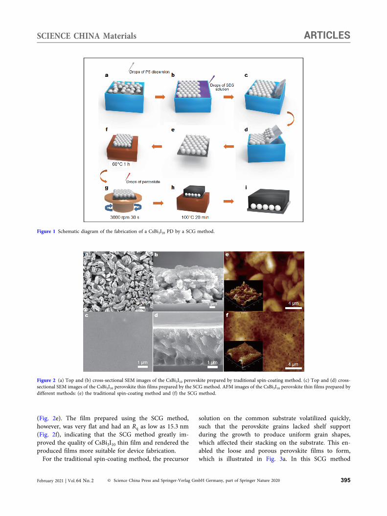
(Fig. 2e). The film prepared using the SCG method,however, was very flat and had an Rq as low as 15.3 nm(Fig. 2f), indicating that the SCG method greatly im-proved the quality of CsBi3I10 thin film and rendered theproduced films more suitable for device fabrication.For the traditional spin-coating method, the precursor
solution on the common substrate volatilized quickly,such that the perovskite grains lacked shelf supportduring the growth to produce uniform grain shapes,which affected their stacking on the substrate. This en-abled the loose and porous perovskite films to form,which is illustrated in Fig. 3a. In this SCG method
Figure 1 Schematic diagram of the fabrication of a CsBi3I10 PD by a SCG method.
Figure 2 (a) Top and (b) cross-sectional SEM images of the CsBi3I10 perovskite prepared by traditional spin-coating method. (c) Top and (d) cross-sectional SEM images of the CsBi3I10 perovskite thin films prepared by the SCG method. AFM images of the CsBi3I10 perovskite thin films prepared bydifferent methods: (e) the traditional spin-coating method and (f) the SCG method.
SCIENCE CHINA Materials. . . . . . . . . . . . . . . . . . . . . . . . . . . . . . . .ARTICLES
February 2021 | Vol. 64 No.2 395© Science China Press and Springer-Verlag GmbH Germany, part of Springer Nature 2020

(Fig. 3b), we used the single-layer PS nanospheres as thetemplate for the SCG of perovskite film. When theCsBi3I10 perovskite precursor solution was spun on the PStemplate, a large amount of precursor solution was lockedamong the PS spheres and the bottom of the perovskiteprecursor among the PS balls first crystallized slowlybecause of the geometry of the confined space, which hadto be filled with less solution. After the samples wereannealed on a hot plate, the evaporation of solvent wasalleviated because of the restricted growth space, whichfurther slowed down the perovskite crystallization processand achieved a higher-quality CsBi3I10 perovskite film[24]. Then, these large-size and high-crystallinity per-ovskite grains among the PS spheres created a seed layerfor the continuous growth of the dense and high-smoothness perovskite film. Finally, we obtained smooth,high-crystallinity, and dense black CsBi3I10 perovskitefilms.The high-quality CsBi3I10 perovskite film by the SCG
encourages us to use it in a PD. According to the XRDpatterns (Fig. 4a), it was evident that the CsBi3I10 per-ovskite thin films prepared by the two methods showedalmost the same diffraction peaks at (003), (006), (300),and other weak peaks, which was consistent with pre-viously reported results [20]. In addition, compared with
Figure 3 The formation mechanism of the CsBi3I10 perovskite filmprepared by the two methods: (a) the traditional spin-coating methodand (b) the SCG method.
Figure 4 Device performances of the CsBi3I10 PDs prepared by the SCG and the traditional spin-coating methods. XRD patterns (a) and absorptioncharacteristics (b) of the CsBi3I10 perovskites. The inset of (b) shows the (αhv)
2 versus hv curves. (c) I–V curves of the CsBi3I10 PDs. (d) I–t curves ofthe SCG CsBi3I10 PD with various light intensities at 5 V. (e) Current versus light intensity curve. The LDR of the PD is 71 dB at 5 V bias.(f) Responsivity and detectivity as a function of the light intensity for the SCG CsBi3I10 PD.
ARTICLES . . . . . . . . . . . . . . . . . . . . . . . . . SCIENCE CHINA Materials
396 February 2021 | Vol. 64 No.2© Science China Press and Springer-Verlag GmbH Germany, part of Springer Nature 2020

the traditionally spin-coated film, the intensity of thediffraction peaks of the CsBi3I10 perovskite thin filmprepared by the SCG was significantly enhanced, in-dicating that the crystallization of perovskite prepared byusing the SCG method improved, which is beneficial forthe device performance. Moreover, the optical absorptioncharacteristic of the CsBi3I10 perovskite thin films isshown in Fig. 4b, and the higher absorption of the SCGCsBi3I10 film displayed higher light harvest efficiencies. Inaddition, the band gap of the SCG CsBi3I10 film showed asmall increase from 1.76 to 1.77 eV, which may be at-tributed to the reduced number of grain defects in thehigh-crystallinity and dense CsBi3I10 perovskite films [25].Fig. 4c shows the I–V curves of the CsBi3I10 PDs, for
which the intensity of the 473 nm laser was370 mW cm−2. Compared with the traditionally spin-coated CsBi3I10 PD with a photocurrent (Ip) of 80 nA anda dark current (Idark) of 2.47 nA at 5 V, the SCG CsBi3I10perovskite film PD showed a larger Ip (169 nA) and asmaller Idark (1.08 nA). This contributed to a bigger on/offratio (156), which was almost five fold that of the tradi-tionally spin-coated CsBi3I10 PD (32). A higher Ip tends togenerate a lower Idark and bigger on/off ratio because thehigh-quality perovskite film prepared by the SCG methodoffered higher light harvest efficiency and faster carrier
separation and transport speed, benefiting superior deviceperformance. The high on/off ratio of the SCG PDs isbeneficial for the performance of the I–t characteristic atdifferent light intensities (0.107 to 370 mW cm−2), asshown in Fig. 4d, wherein we observed good repeatabilityand stable Ip and Idark. In addition, an increase in the lightintensity generated an almost linear Ip increase. Linearfitting of the data produced a R2 coefficient of 0.98621 forthe CsBi3I10 PD (Fig. 4e), which indicated that the denseCsBi3I10 film had a good ability to collect photogeneratedcarriers. This ability can be characterized by the LDR:LDR=20log(Psat/Plow), (1)where Psat(Plow) is the optical power when the incidentlight intensity is stronger(weaker) than that at which thephotocurrent begins to deviate from linearity. When thelight intensity increased from 0.107 to 370 mW cm−2, thecurrent increased from the Idark of 37 nA cm−2 to6.05 μA cm−2, corresponding to an LDR of 71 dB. Fromthe responsivity and detectivity of the SCG PD shown inFig. 4f, we obtained optimal responsivity and detectivityvalues of 0.45 mA W−1 and 4.14 × 10⁹ Jones, respectively.Fig. 5a shows the response time curve of the device at
5 V, which shows a rising time of 0.62 ms and a fallingtime of 0.81 ms, demonstrating a fast response speed thatis comparable to those of other lead-free MSM structural
Figure 5 (a) Time response of the device under 5 V bias. (b) Normalized spectral photoresponse of the MSM PD at 5 V bias. (c) Normalized I–t curve ofthe PD without encapsulation in air for 30 min. The intensity of the 473 nm laser is 7.54 mW cm−2. (d) I–t attenuation curves of the device within 30 d.
SCIENCE CHINA Materials. . . . . . . . . . . . . . . . . . . . . . . . . . . . . . . .ARTICLES
February 2021 | Vol. 64 No.2 397© Science China Press and Springer-Verlag GmbH Germany, part of Springer Nature 2020

devices (Table S1). Fig. 5b shows the normalized re-sponsivity versus the wavelength curve, which shows amaximum responsivity at 670 nm. As the wavelengthdecreased, the device responsivity decreased.Device stability is crucial for its commercialization.
Fig. 5c shows the stability of our unencapsulated devicewhen it was continuously irradiated with a laser for30 min in air at 473 nm and with a light intensity of7.45 mW cm−2. Although our device was not en-capsulated, the photocurrent of the device had almost noattenuation, illustrating the long-time operation stabilityof our devices under conditions with and without light.Fig. 5d presents the I–t curves after long-term storage ofour unencapsulated devices (conditions: room tempera-ture of 25°C; 60% humidity in air). After 17 and 30 d, thephotocurrent of our device showed no degradation. Theultra-high stability of our SCG CsBi3I10 perovskite filmwas attributed to (1) the good tolerance of the all-inorganic CsBi3I10 to water and air; and (2) the SCGmethod using the PS template for growing a flat, dense,and pinhole-free CsBi3I10 perovskite thin film with highcrystallinity, which effectively blocked the penetration ofwater and oxygen in the air and improved the stability ofthe device. In comparison, the CsBi3I10 perovskite filmprepared by the traditional spin-coating method showedsignificant degradation, and its color changed from blackto red after storage in air for three months, which furtherconfirmed the degradation by using the XRD patterns(Fig. S4).
CONCLUSIONSIn the present study, the CsBi3I10 perovskite films wereprepared by SCG without any antisolvent. These filmsshowed higher crystal quality and better optical proper-ties compared with traditionally spin-coated films. Theperformance of the MSM PD prepared by SCG was betterthan that of the traditionally spin-coated CsBi3I10 PD. Inaddition, the photocurrent of the SCG device showed nodegradation when it was illuminated for 30 min or storedin air for 30 d, demonstrating its ultra-high stability. Thiswork opens up a new way to prepare high-quality lead-free perovskite, which may be useful for applications inmany fields, such as light-emitting diodes and solar cells.
Received 18 May 2020; accepted 1 July 2020;published online 9 October 2020
1 Mahabadi SEJ, Wang S, Carruthers TF, et al. Calculation of theimpulse response and phase noise of a high-current photodetectorusing the drift-diffusion equations. Opt Express, 2019, 27: 3717–3730
2 Zhou H, Zhu Y, Wang H, et al. Electroluminescence transitionfrom visible- to ultraviolet-dominant mode in n-Mn0.04Zn0.96O/i-ZnGa2O4/n-GaN structure with highly ultraviolet detection per-formance. IEEE Electron Device Lett, 2013, 34: 423–425
3 Han L, Peng M, Wen Z, et al. Self-driven photodetection based onimpedance matching effect between a triboelectric nanogeneratorand a MoS2 nanosheets photodetector. Nano Energy, 2019, 59:492–499
4 Cao Y, Wang N, Tian H, et al. Perovskite light-emitting diodesbased on spontaneously formed submicrometre-scale structures.Nature, 2018, 562: 249–253
5 Lin K, Xing J, Quan LN, et al. Perovskite light-emitting diodes withexternal quantum efficiency exceeding 20 percent. Nature, 2018,562: 245–248
6 Feng J, Gong C, Gao H, et al. Single-crystalline layered metal-halide perovskite nanowires for ultrasensitive photodetectors. NatElectron, 2018, 1: 404–410
7 Burschka J, Pellet N, Moon SJ, et al. Sequential deposition as aroute to high-performance perovskite-sensitized solar cells. Nature,2013, 499: 316–319
8 Lee MM, Teuscher J, Miyasaka T, et al. Efficient hybrid solar cellsbased on meso-superstructured organometal halide perovskites.Science, 2012, 338: 643–647
9 Domanski K, Alharbi EA, Hagfeldt A, et al. Systematic investiga-tion of the impact of operation conditions on the degradationbehaviour of perovskite solar cells. Nat Energy, 2018, 3: 61–67
10 Babayigit A, Ethirajan A, Muller M, et al. Toxicity of organometalhalide perovskite solar cells. Nat Mater, 2016, 15: 247–251
11 Tong J, Song Z, Kim DH, et al. Carrier lifetimes of >1 μs in Sn-Pbperovskites enable efficient all-perovskite tandem solar cells. Sci-ence, 2019, 36: 475–479
12 Hao F, Stoumpos CC, Cao DH, et al. Lead-free solid-state organic–inorganic halide perovskite solar cells. Nat Photon, 2014, 8: 489–494
13 Ke W, Kanatzidis MG. Prospects for low-toxicity lead-free per-ovskite solar cells. Nat Commun, 2019, 10: 965
14 Ji C, Wang P, Wu Z, et al. Inch-size single crystal of a lead-freeorganic-inorganic hybrid perovskite for high-performance photo-detector. Adv Funct Mater, 2018, 28: 1705467
15 Wang W, Zhao D, Zhang F, et al. Highly sensitive low-bandgapperovskite photodetectors with response from ultraviolet to thenear-infrared region. Adv Funct Mater, 2017, 27: 1703953
16 Waleed A, Tavakoli MM, Gu L, et al. Lead-free perovskite nano-wire array photodetectors with drastically improved stability innanoengineering templates. Nano Lett, 2016, 17: 523–530
17 Du Z, Fu D, Yang T, et al. Photodetectors with ultra-high de-tectivity based on stabilized all-inorganic perovskite CsPb0.922Sn0.078I3 nanobelts. J Mater Chem C, 2018, 6: 6287–6296
18 Zhu HL, Liang Z, Huo Z, et al. Low-bandgap methylammonium-rubidium cation Sn-rich perovskites for efficient ultraviolet-visible-near infrared photodetectors. Adv Funct Mater, 2018, 28: 1706068
19 Liao Y, Liu H, Zhou W, et al. Highly oriented low-dimensional tinhalide perovskites with enhanced stability and photovoltaic per-formance. J Am Chem Soc, 2017, 139: 6693–6699
20 Johansson MB, Zhu H, Johansson EMJ. Extended photo-conver-sion spectrum in low-toxic bismuth halide perovskite solar cells. JPhys Chem Lett, 2016, 7: 3467–3471
21 Brandt RE, Kurchin RC, Hoye RLZ, et al. Investigation of bismuthtriiodide (BiI3) for photovoltaic applications. J Phys Chem Lett,2015, 6: 4297–4302
ARTICLES . . . . . . . . . . . . . . . . . . . . . . . . . SCIENCE CHINA Materials
398 February 2021 | Vol. 64 No.2© Science China Press and Springer-Verlag GmbH Germany, part of Springer Nature 2020

22 Park BW, Philippe B, Zhang X, et al. Bismuth based hybrid per-ovskites A3Bi2I9 (A: methylammonium or cesium) for solar cellapplication. Adv Mater, 2015, 27: 6806–6813
23 Liu R, Zhou H, Song Z, et al. Low-reflection, (110)-orientation-preferred CsPbBr3 nanonet films for application in high-perfor-mance perovskite photodetectors. Nanoscale, 2019, 11: 9302–9309
24 Zeng J, Li X, Wu Y, et al. Space-confined growth of CsPbBr3 filmachieving photodetectors with high performance in all figures ofmerit. Adv Funct Mater, 2018, 28: 1804394
25 Ke X, Yan J, Zhang A, et al. Optical band gap transition from directto indirect induced by organic content of CH3 NH3PbI3 perovskitefilms. Appl Phys Lett, 2015, 107: 091904
Acknowledgements This work was supported by the National NaturalScience Foundation of China (51972101 and 11874143), the NaturalScience Foundation of Hubei Province (2019CFB508), and WuhanYellow Crane Talent Program (2017-02).
Author contributions Liu R designed the research and performed thedata processing. Wang R, Wu D, Pan X, and Pan G interpreted the data.Liu R and Zhou H co-wrote and revised the manuscript. Zhou H andWang H provided experimental support.
Conflict of interest The authors declare no conflict of interest.
Supplementary information Supporting data are available in theonline version of the paper.
Ronghuan Liu received his BE degree fromHubei University of China in 2016. He is cur-rently a MSc candidate at Hubei University,under the supervision of Prof. Hai Zhou. Hiscurrent research focuses on perovskite photo-detectors.
Hai Zhou received his MSc and PhD degrees inmicroelectronics and solid state electronics fromWuhan University, China. He is currently anAssociate Professor of Hubei Key Laboratory ofFerroelectric and Dielectric Materials and De-vices, Faculty of Physics and Electronic Science,Hubei University, China. His main research in-terests include Ga2O3 ultraviolet photodetectors,and perovskite photodetectors based on micro/nano structures.
Hao Wang is Chair Professor of the Faculty ofPhysics and Electronic Science and Dean ofGraduate School of Hubei University. He re-ceived his PhD from Huazhong University ofScience and Technology in 1994 and worked as apostdoctor at Peking University and the ChineseUniversity of Hong Kong till 2002. Before hejoined Hubei University, he was appointed asprofessor of Shanghai Jiao Tong University in2002. He is a visiting professor of the Universityof Cambridge and Aalto University. His current
research interests involve energy and information applications ofnanostructured materials including solar cells, fuel cells, non-volatilememory and optoelectronic devices, and magnetic nanostructures.
空间限域生长CsBi3I10无铅钙钛矿用于高质量、高灵敏度和高稳定性近红外光电探测器刘荣桓, 周海*, 王瑞, 吴定军, 潘希彦, 潘广东, 王浩*
摘要 因具有较高的耐热性和较长的电子扩散长度, 无铅钙钛矿CsBi3I10备受关注. 然而, 由于二维结构CsBi3I10钙钛矿的表面极其粗糙且存在大量针孔, 导致CsBi3I10钙钛矿器件性能不高. 本文报道了一种利用空间限域生长(SCG)获得高平滑度、高结晶度和致密CsBi3I10钙钛矿薄膜的方法. 相对于传统旋涂法制备的探测器, 采用SCG方法获得的金属-半导体-金属结构CsBi3I10光电探测器(PDs)具有更高的光电流、更低的暗电流, 以及更大的开/关比. 此外, 在长时间测试下, 未封装的CsBi3I10钙钛矿PDs的光电流没有衰减; 在空气中储存30天后, 器件的性能也没有明显的退化, 表现出了超高的稳定性. 研究表明空间限域生长方法为制备高质量无铅钙钛矿开辟了一条新途径, 有望在发光二极管、太阳能电池等领域得到应用.
SCIENCE CHINA Materials. . . . . . . . . . . . . . . . . . . . . . . . . . . . . . . .ARTICLES
February 2021 | Vol. 64 No.2 399© Science China Press and Springer-Verlag GmbH Germany, part of Springer Nature 2020