space qualification of rf mems switches in silicon ... g. bartolucci (cnr-imm roma and university of...
TRANSCRIPT
SPACE QUALIFICATION OFRF MEMS SWITCHES IN SILICON TECHNOLOGY
FOR REDUNDANCY APPLICATIONSSupported by the ESA Contract on "High Reliability MEMS Redundancy Switch"
B. Margesin, V. Mulloni, F. Giacomozzi (FBK); F. Vitulli, M. Scipioni (TAS-I); A. Lucibello, G. Capoccia, E. Proietti, R. Marcelli (CNR-IMM Roma); G. Bartolucci (CNR-IMM Roma and University of Roma Tor Vergata);
Paola Farinelli (RF Microtech and University of Perugia); Gaudenzio Meneghesso, Marco Barbato (University of Padova)
LTCC TECHNOLOGYFOR RF MEMS FABRICATION AND PACKAGING
Supported by the MIUR Project SAPERE-SAFE
Andrea Lucibello and Romolo Marcelli (CNR-IMM Roma) Ernesto Di Paola, Stefano Croci and Chiara Germani (TAS-I)
[email protected] - http://www.artov.imm.cnr.itComponents4Space, Italian Space Agency – 18-20 January 2016
..

NATIONAL RESEARCH COUNCILINSTITUTE FOR MICROLECTRONICSAND MICROSYSTEMS (CNR -IMM)
The Institute for Microelectronics and Microsystems(IMM) belongs to the Department for PhysicalSciences and Technologies for Matter (DSFTM) ofCNR, and it is currently organized on Seven Sitesand four different main Research Lines
(currently under revision):a) materials, processes and devices for microelectronics; b) sensors and micro-systems; c) optoelectronics and photo-voltaics; d) development of advanced characterization techniques for
material and process analyses.Web: http://www.imm.cnr.it
More than 200 permanent Reasearchers and Technicians, involved in theabove defined areas, and 20% to 40% are presently or potentially involvedin micro-electronics and micro-system activities including design,technology, test and modeling for Space and Security.Reliability criteria valid for space as well as defence and commercialapplications are followed for releasing the feasibility of devices andsub-systems.
2
IMMRoma
Medium Size Clean Room capabilities (300 – 500 m2) in Class from 100.000 down to 100, equipped for micro- to nano-electronics as well as for micro- and nano-systems, are availablein several sites of the Department. Thin film deposition techniques with multi-layer maskprocesses are routinely done.
Potential small size production of on-wafer sub-systems can be pursued, and full characterization including on-line and off-line measurements can be performed (maskmanufacturing, chemical and physical etching techniques, micromachining, …).
Morphology, mechanical characteristics, doping profiles, etc . for sub-micron and nano-devices are evaluated by means of purposely built setups and commercial instruments (SEM, TEM, Digital Holography, Micro-analysis, Scanning Probe Microscopy, …).
Electrical DC and RF characterization is provided by using calibrated and remotely controllednetwork equipments (Time and Frequency Domain for IR, Microwave, mm-wave and OpticalDevices and Sub-Systems).
Modeling by means of home made and commercial codes for specific problems, includingthermal and power handling, fluido-dynamics, EM propagation , charging processes, …. are part of the skill in every site.
FACILITIES
3
The Institute participates to activities managed within the Aerospace Technological Districts (DTAs)
at regional and national level
Reference Technological National Platforms: SPIN-IT (SPACE) and SERIT (SECURITY)
The main commitment in Space Business comes from the major National Companies and Groups, like
FINMECCANICA, TAS, CGS, STMicroelectronics … and SME and their Associations (AIPAS, AIAD, ASAS).
RELATIONSHIPS WITH COMPANIESAND INSTITUTIONAL STAKEHOLDERS
4

•Telecom Applications in the Microwave and Millimeter Wave Range•Structural characterization for avionics by means of optical fiber sensing•Photo-voltaic ground applications suitable of Space implementations•Material Science on nano-structured materials for nano-interconnections, sensing and radiation hardness improvement•High K materials•Sensing for life quality in ground and on-board environments•Novel concepts in detection and signal processing of RF, THz and opticalsignals
TAXONOMY (following SPIN-IT Definitions)
….
SOME HIGHLIGHTS OF THE IMM SPACE RELATED ACTIVITIES (NOT EXHAUSTIVE)
5ThermomechanicsThermomechanics
OpticsOpticsStructuresStructures
MaterialsMaterials
PhotonicsPhotonics
ElectronicsElectronics
TA1 TA2
MechanismsMechanisms
Integrated sensors, cryogenic components
Integrated sensors, cryogenic components
Telecommunication Systems Security
OUTLINE
IntroductionRF MEMS switches in Silicon technologySPST, SPDT configurations for
redundancy applicationsLTCC packaging of SPDT in Silicon
technologyRF MEMS switches in LTCC technology
and packaging6Components4Space, Italian Space Agency – 18-20 January 2016
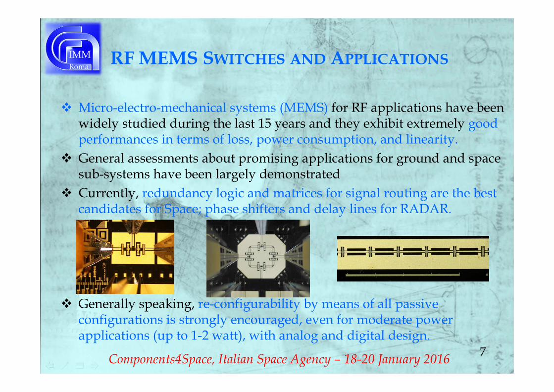
RF MEMS SWITCHES AND APPLICATIONS
Micro-electro-mechanical systems (MEMS) for RF applications have been widely studied during the last 15 years and they exhibit extremely good performances in terms of loss, power consumption, and linearity.
General assessments about promising applications for ground and space sub-systems have been largely demonstrated
Currently, redundancy logic and matrices for signal routing are the best candidates for Space; phase shifters and delay lines for RADAR.
Generally speaking, re-configurability by means of all passive configurations is strongly encouraged, even for moderate powerapplications (up to 1-2 watt), with analog and digital design.
7Components4Space, Italian Space Agency – 18-20 January 2016
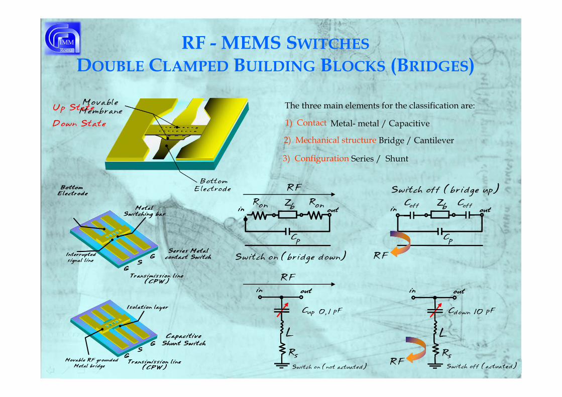
RF - MEMS SWITCHESDOUBLE CLAMPED BUILDING BLOCKS (BRIDGES)
The three main elements for the classification are:
1) Contact Metal- metal / Capacitive
2) Mechanical structure Bridge / Cantilever
3) Configuration Series / Shunt

Actuation voltage
Pull-down
Gold beam
RF - MEMS SWITCHESSINGLE CLAMPED BUILDING BLOCKS (CANTILEVERS)
Components4Space, Italian Space Agency – 18-20 January 2016

DESIGN CRITERIA• The RF MEMS switch consists of a double
clamped gold beam, anchored on the two ground planes of a coplanar waveguide structure.
• The actuation is provided pulling down electrostatically the bridge because of the mechanical force generated by means of the voltage applied at the two lateral actuation electrodes (DC and RF signals are decoupled).
• The dielectric is removed from the lateral actuation pads to minimize charging phenomena; mechanical stoppers patterned on the substrate prevent the contact between the metal beam in the down-state and the actuation pads.
10
Contact Area
Actuation electrodes
RF I/O RF I/O
Components4Space, Italian Space Agency – 18-20 January 2016
RF MEMS SPST PERFORMANCES
• Generally, performances for RF MEMS SPST devices are:
isolation better than 20 dB, insertion losses not exceeding 0.3-0.4 dB for
wideband applications. • The shunt capacitive configuration is intrinsically
limited in band because of its resonant response.• The ohmic series device is designed to have a
broadband response. • Actuations up to 107-108 or more
Components4Space, Italian Space Agency – 18-20 January 2016

ISSUES FOR RF MEMS
12
Contact deterioration upon cycling is one of the most investigated failure mechanisms for MEMS RF-switches, and the role of the contact material appears to be of paramount importance.
Two important parameters to be checked are: (i) the contact resistance, which should be as low as possible, and (ii) the number of cycles, to be maximized without alterations in the RF performances.
In several applications it would be desirable to have a contact resistance not exceeding 1 Ω, and a cycling reliability up to, at least, 107 actuations during the switch operation, which is particularly appealing when compared to classical p-i-n diode switches.
Charging effects are responsible for sticking of the actuated metal membranes, and can be controlled (or mitigated) by means of dielectric-less actuation configurations or by using substrates not affected by charging at all.
Components4Space, Italian Space Agency – 18-20 January 2016

Charging effects mitigationThe dependence of the exploited devices on the chargingphenomena has been mitigated by means of dielectric pillars, manufactured under the metal beam to prevent the full contact between the bridge and the dielectric lateral pads used for the electrostatic actuation.
Pillars geometry
Shunt capacitive Ohmic series
Components4Space, Italian Space Agency – 18-20 January 2016

CONTACT MATERIALS• Stacking layers of platinum between gold layers can improve not only
the hardness but also the surface properties of gold commonly used in RF-switch contacts.
• The roughness of the contact surface is reduced and the tendency of platinum for frictional polymers is maintained under control, because the surface exposed to ambient is made of gold.
14Components4Space, Italian Space Agency - 19 January 2016
Two material variants: (i) pure gold in the“reference” device and (ii) a modifiedmultilayer composed of a thin (3 nm)platinum layer sandwiched between twothicker layers of gold with thicknesses of120 nm (bottom) and 30 nm (top) of goldin the “test” device.
In the “test” device the bottom part of themobile membrane was also made with 150nm of the same material, in order to havecontacting surfaces with the samecharacteristics on both sides.

PRELIMINARY TEST RESULTS
15
RF performances at first actuation for the standard switch (reference device) and the switch with the modified contact
material (test switch). Comparison between measured transmission and equivalent circuit fit (a), and isolation (b)
(a) (b)
Components4Space, Italian Space Agency – 18-20 January 2016
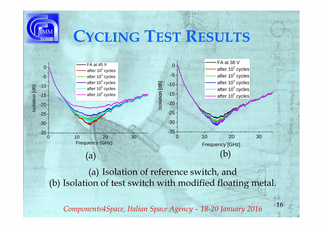
CYCLING TEST RESULTS
16
0 10 20 30-35
-30
-25
-20
-15
-10
-5
0
Isol
atio
n [d
B]
FA at 45 V after 102 cycles after 103 cycles after 104 cycles after 105 cycles after 106 cycles
Frequency (GHz)0 10 20 30
-35
-30
-25
-20
-15
-10
-5
0
Isol
atio
n [d
B]
Frequency [GHz]
FA at 38 V after 102 cycles after 103 cycles after 104 cycles after 105 cycles after 106 cycles
(a) Isolation of reference switch, and (b) Isolation of test switch with modified floating metal.
(a) (b)
Components4Space, Italian Space Agency – 18-20 January 2016

CONTACT RESISTANCE
The surface characteristics are also different for the two contact materials, when they experience the conditions of a typical switch fabrication process. Contact region surface morphology in the reference device (left) and in the
modified test device (right). 17
Switch Rcontact (ohm)(initial value)
Rcontact (ohm)(after 106 cycles)
Reference 0.75 2.36Test 1.00 0.70
Material HardnessValue
Gold 2.2Multilayer 3.0
Components4Space, Italian Space Agency – 18-20 January 2016
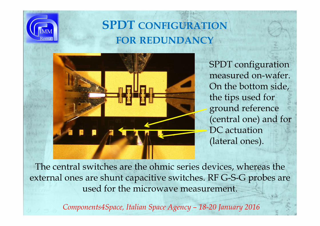
SPDT CONFIGURATIONFOR REDUNDANCY
SPDT configuration measured on-wafer. On the bottom side, the tips used for ground reference (central one) and for DC actuation (lateral ones).
The central switches are the ohmic series devices, whereas the external ones are shunt capacitive switches. RF G-S-G probes are
used for the microwave measurement.
Components4Space, Italian Space Agency – 18-20 January 2016
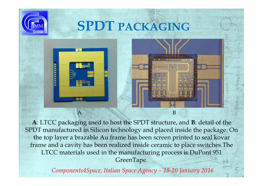
SPDT PACKAGING
A: LTCC packaging used to host the SPDT structure, and B: detail of the SPDT manufactured in Silicon technology and placed inside the package. On
the top layer a brazable Au frame has been screen printed to seal kovarframe and a cavity has been realized inside ceramic to place switches.The
LTCC materials used in the manufacturing process is DuPont 951 GreenTape.
A B
Components4Space, Italian Space Agency – 18-20 January 2016
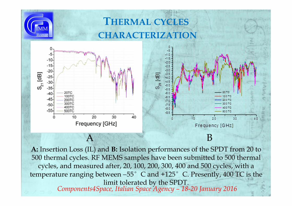
THERMAL CYCLESCHARACTERIZATION
A: Insertion Loss (IL) and B: Isolation performances of the SPDT from 20 to 500 thermal cycles. RF MEMS samples have been submitted to 500 thermal
cycles, and measured after, 20, 100, 200, 300, 400 and 500 cycles, with a temperature ranging between 55°C and +125°C. Presently, 400 TC is the
limit tolerated by the SPDT.
A B
Components4Space, Italian Space Agency – 18-20 January 2016
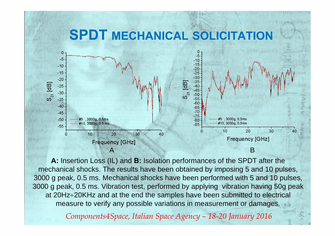
SPDT MECHANICAL SOLICITATION
A: Insertion Loss (IL) and B: Isolation performances of the SPDT after the mechanical shocks. The results have been obtained by imposing 5 and 10 pulses,
3000 g peak, 0.5 ms. Mechanical shocks have been performed with 5 and 10 pulses, 3000 g peak, 0.5 ms. Vibration test, performed by applying vibration having 50g peak
at 20Hz20KHz and at the end the samples have been submitted to electrical measure to verify any possible variations in measurement or damages.
A B
Components4Space, Italian Space Agency – 18-20 January 2016
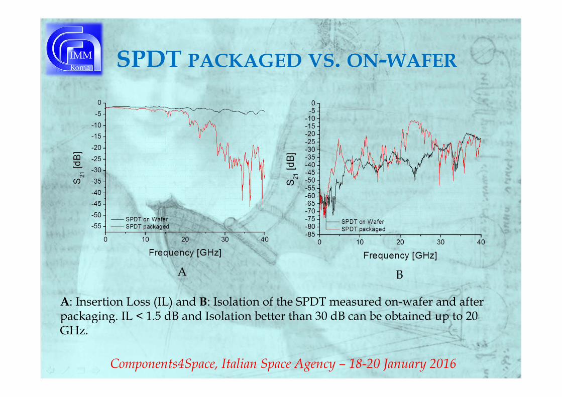
SPDT PACKAGED VS. ON-WAFER
A: Insertion Loss (IL) and B: Isolation of the SPDT measured on-wafer and after packaging. IL < 1.5 dB and Isolation better than 30 dB can be obtained up to 20 GHz.
A B
Components4Space, Italian Space Agency – 18-20 January 2016
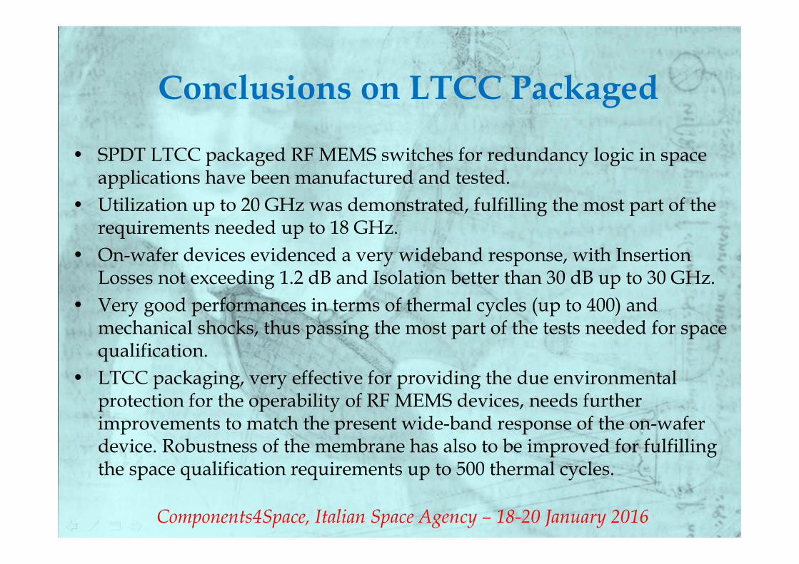
Conclusions on LTCC Packaged
• SPDT LTCC packaged RF MEMS switches for redundancy logic in space applications have been manufactured and tested.
• Utilization up to 20 GHz was demonstrated, fulfilling the most part of the requirements needed up to 18 GHz.
• On-wafer devices evidenced a very wideband response, with Insertion Losses not exceeding 1.2 dB and Isolation better than 30 dB up to 30 GHz.
• Very good performances in terms of thermal cycles (up to 400) and mechanical shocks, thus passing the most part of the tests needed for space qualification.
• LTCC packaging, very effective for providing the due environmental protection for the operability of RF MEMS devices, needs further improvements to match the present wide-band response of the on-wafer device. Robustness of the membrane has also to be improved for fulfilling the space qualification requirements up to 500 thermal cycles.
Components4Space, Italian Space Agency – 18-20 January 2016
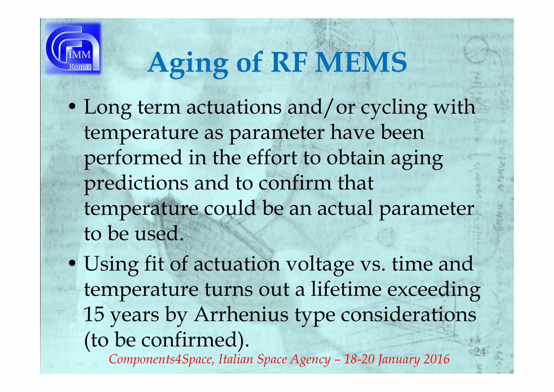
Aging of RF MEMS• Long term actuations and/or cycling with
temperature as parameter have beenperformed in the effort to obtain agingpredictions and to confirm thattemperature could be an actual parameterto be used.
• Using fit of actuation voltage vs. time and temperature turns out a lifetime exceeding15 years by Arrhenius type considerations(to be confirmed).
24Components4Space, Italian Space Agency – 18-20 January 2016

RF MEMS IN LTCC TECHNOLOGY
• Low Temperature Co-fired Ceramics (LTCC) is a well established technology for down-sizing RF modules containing buried components and interconnections.
• LTCC has been evaluated for integrating surface micro-machined RF MEMS switches and packaging of modules for space applications, including SPST, SPDT and DPDT for redundancy purposes, with the aim of obtaining a fully integrated structure.
• Advantages coming from the main characteristics of the MEMS configuration, like no signal distortion and low losses are expected.
• Negligible charging effects are expected from such a material with respect to the electro-mechanical response of the switches.
25
• The implementation of matrix configurations for signal routing is currently evaluated, to manufacture modules characterized by high complexity and a fully passive solution. Sub-systems composed by a number of DPDT sub-matrices suitable to be integrated in a 12x12 configuration can be designed and their manufacturing was already demonstrated in silicon technology.
Components4Space, Italian Space Agency – 18-20 January 2016
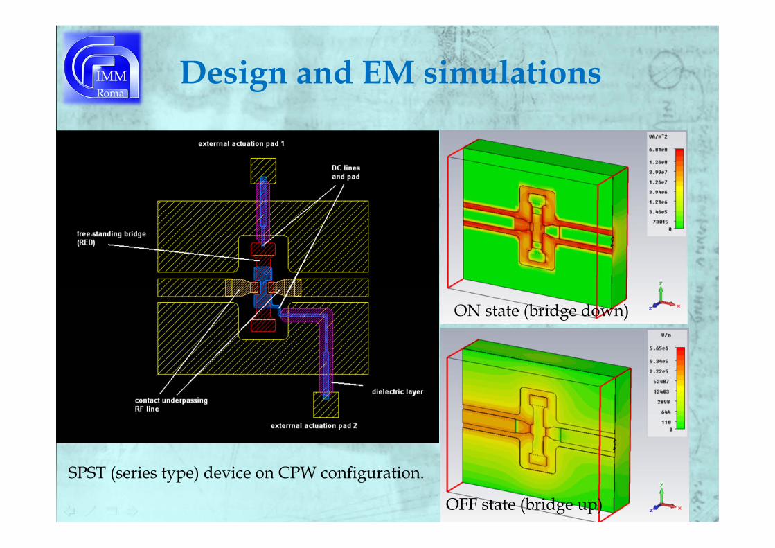
Design and EM simulations
26SPST (series type) device on CPW configuration.
ON state (bridge down)
OFF state (bridge up)

Transm
ission
Isolation
0 10 20 30 40
-90
-80
-70
-60
-50
-40
-30
-20
-10
0
Isol
atio
n [d
B]
Frequency [GHz]
B1-D2 S21
B1-D2 S21 after 102
B1-D2 S21 103
B1-D2 S21 104
B1-D2 S21 after 2x10⁴
B1-D2 S21 after 7x10⁴
B1-D2 S21 after 105
B1-D2 S21 after 2x10⁵
B1-D2 S21 after 7x10⁵
B1-D2 S21 after 106
B1-D2 S21 after 2x10⁶
0 10 20 30 40-40
-35
-30
-25
-20
-15
-10
-5
0
Ret
urn
Loss
[dB
]
Frequency [GHz]
B1-D2 S11
B1-D2 S11 after 102
B1-D2 S11 after 103
B1-D2 S11 after 104
B1-D2 S11 after 2x10⁴
B1-D2 S11 after 7x10⁴
B1-D2 S11
after 105
B1-D2 S11 after 2x10⁵
B1-D2 S11 after 7x10⁵
B1-D2 S11 after 106
B1-D2 S11 after 2x10⁶
0 10 20 30 40
-2.0
-1.8
-1.6
-1.4
-1.2
-1.0
-0.8
-0.6
-0.4
-0.2
0.0
B1-D2 S21
B1-D2 S21 after 102
B1-D2 S21 after 103
B1-D2 S21 after 104
B1-D2 S21 after 2x10⁴
B1-D2 S21 after 7x10⁴
B1-D2 S21 after 105
B1-D2 S21 after 2x10⁵
B1-D2 S21 after 7x10⁵
B1-D2 S21 after 106
B1-D2 S21 after 2x10⁶
Inse
rtion
Los
s [d
B]
Frequency [GHz]
Name CyclesVmax
[V]Vdeact [V]
B1‐D2
100 50 38
102 50 42
103 48 42
104 48 42
2x10⁴ 48 40
7x10⁴ 48 42
105 48 42
2x10⁵ 48 42
7x10⁵ 48 42
106 95 34
2x10⁶ 115 34
SPST
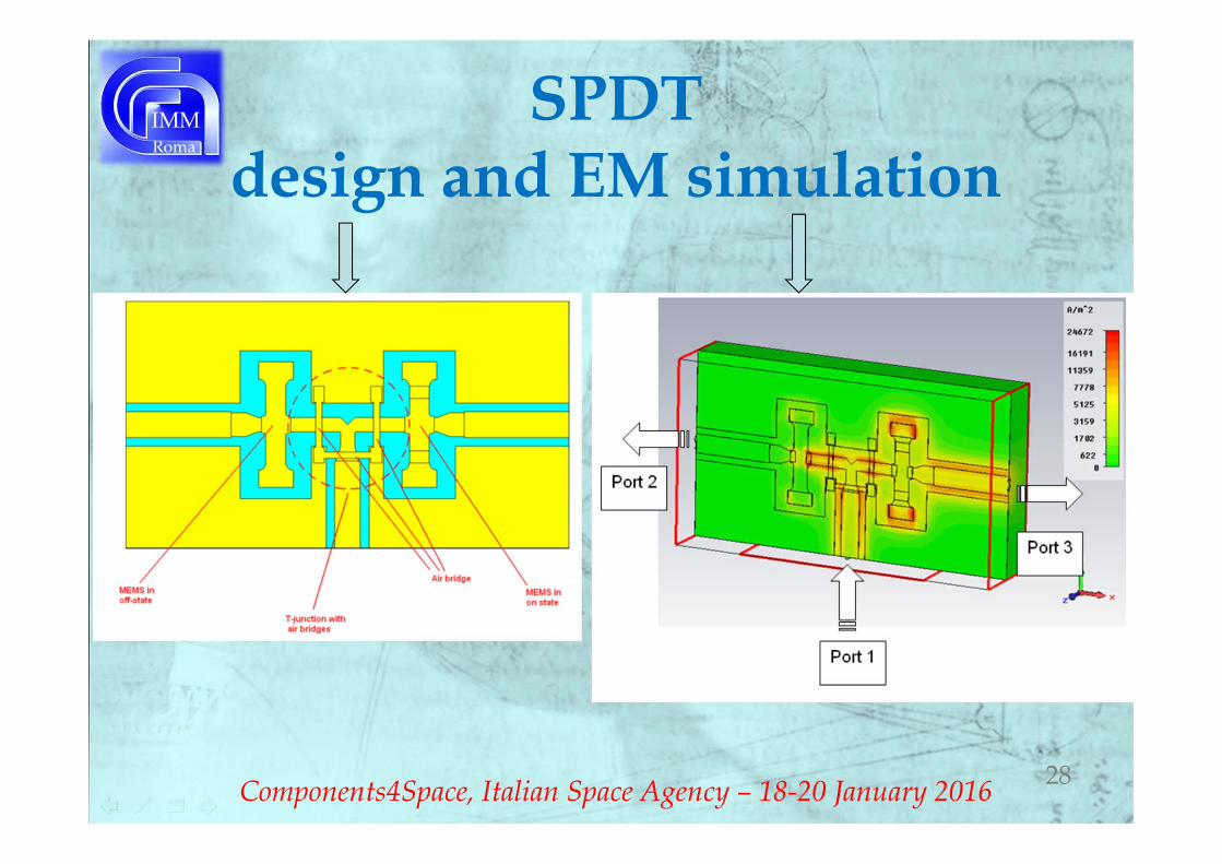
SPDT design and EM simulation
28Components4Space, Italian Space Agency – 18-20 January 2016
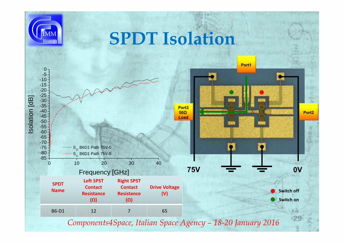
SPDT Isolation
29
0 10 20 30 40-85-80-75-70-65-60-55-50-45-40-35-30-25-20-15-10-50
S11 B6D1 Path 75V-0 S21 B6D1 Path 75V-0
Isol
atio
n [d
B]
Frequency [GHz] 75V 0V
Port350Ω Load
Port2
Port1
Switch off
Switch on
SPDTName
Left SPSTContact
Resistance (Ω)
Right SPST Contact
Resistance (Ω)
Drive Voltage(V)
B6‐D1 12 7 65
Components4Space, Italian Space Agency – 18-20 January 2016

SPDT Insertion Loss
30
0 10 20 30 40
-4.0
-3.5
-3.0
-2.5
-2.0
-1.5
-1.0
-0.5
0.0
S21 B6D1 Path 0-75V
Inse
rtion
Los
s [d
B]
Frequency [GHz] 0V 75V
Port350Ω Load
Port2
Port1
Switch off
Switch on
SPDTName
Left SPSTContact
Resistance (Ω)
Right SPST Contact
Resistance (Ω)
Drive Voltage(V)
B6‐D1 12 7 65
Components4Space, Italian Space Agency – 18-20 January 2016

SPDT Return Loss
31
0 10 20 30 40-26-24-22-20-18-16-14-12-10-8-6-4-20
S11 B6D1 Path 0-75V
Ret
urn
Loss
[dB
]
Frequency [GHz] 0V 75V
Port350Ω Load
Port2
Port1
Switch off
Switch on
SPDTName
Left SPSTContact
Resistance (Ω)
Right SPST Contact
Resistance (Ω)
Drive Voltage(V)
B6‐D1 12 7 65
Components4Space, Italian Space Agency – 18-20 January 2016

DPDT (2x2 Matrix)Design and EM simulation
32Components4Space, Italian Space Agency – 18-20 January 2016
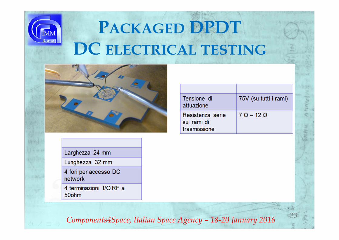
PACKAGED DPDTDC ELECTRICAL TESTING
33Components4Space, Italian Space Agency – 18-20 January 2016
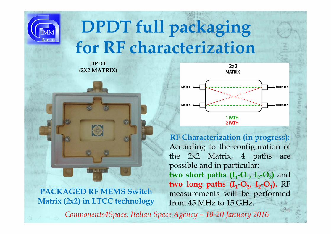
DPDT full packagingfor RF characterization
34
PACKAGED RF MEMS Switch Matrix (2x2) in LTCC technology
RF Characterization (in progress):According to the configuration ofthe 2x2 Matrix, 4 paths arepossible and in particular:two short paths (I1-O1, I2-O2) andtwo long paths (I1-O2, I2-O1). RFmeasurements will be performedfrom 45 MHz to 15 GHz.
DPDT(2X2 MATRIX)
Components4Space, Italian Space Agency – 18-20 January 2016
Past and currentRF MEMS Contracts and Cooperations
with Italian Partners - 1• European Project on a 38 GHz micromachined TX/RX module in
alumina and silicon technology: membrane supported, micromachinedantennas (1998-2002).
• ASI Project "Microsistemi a Microonde ed Onde Millimetriche per Applicazioni Spaziali» for membrane supported micromachinedlumped components and filters
35Components4Space, Italian Space Agency – 18-20 January 2016

Past and currentRF MEMS Contracts and Cooperations
with Italian Partners - 2• European Space Agency (ESA) contracts on RF MEMS switches in
silicon technology for: (i) SPST and SPDT configurations and their space qualification, (ii) redundancy applications and (iii) matrices for signal routing in satellite reconfiguration (2002 – 2015).
• ST-Microelectronics (Agrate Brianza) contract, on “Design, modeling and test of microswitches” (2007)
36

Past and currentRF MEMS Contracts and Cooperations
with Italian Partners - 3• European Defence Agency (EDA) contract on delay lines and phase shifters
for beam forming networks in radar applications (2006-2009).
• MIUR contract “TASMA” (Tecnologie Abilitanti per Sistemi di Monitoraggio Aeroportuale) on medium power RF MEMS and packaging (2014-2016).
• Aerospace National Technology Cluster (CTNA) activities, supported by the Italian Ministry for Research and Education (MIUR) on RF MEMS packaged configurations for signal routing in LTCC technology to be used in small aperture radar (SAR) modules (2014-2016).
37

38
RF MEMS Technology Purpose Cost Advantages Drawbacks
Sacrificial LayerRelease
Micromachining
Silicon Devices, 2D/3D Microsystems Low-Medium reliable, low loss
low-medium power, charging to be
mitigated
Photoresist: high pressure O2 plasma process performed in
asher
GaAs Devices, 2D/3D Microsystems Medium-High reliable, low loss
Not completelyCMOS compatible,
charging (?)
Photoresist: high pressure O2 plasma process performed in
a barrel etcher
AluminaDevices, 2D
Structures, low-level packaging
Low-Medium medium-high power, well established
surface roughness, lossy
SiO2: Wet etching with subsequent rinse
in water/IPA/cyclohexan
e and freeze and sublimation
LTCCDevices, 2D/3D Microsystems,
PackagingLow 3D integrability
surface roughness, shrinking effect after LTCC cofiring, lossy
SiO2: Wet etching with subsequent rinse
in water/IPA/cyclohexan
e and freeze and sublimation
SU-8Devices, 2D/3D Microsystems,
PackagingLow Photolithographic
processing
breakdown voltage, outgassing to be
confirmed, sacrificial layer removal
(viscosity)
Resist or SU-8: wet or O2 assisted RIE
Next Future GoalsMicro- and Nano-Systems for low and high frequency components andsub-systems with functionalities quite different between them (electrical orelectromagnetic, electro-mechanical, and chemical-physical) to be integrated inthe same configuration. with special care to :
i. Optimization of bulk and surface micromachining techniques fordifferent substrates which can host configurations for guided andfree space propagation as well as resonating structures and nano-devices
ii. Design and realization of innovative components, for which nocommercial software solution exists for the full design, especiallywhen different and/or combined solicitations are involved;
iii. Reliability of Micro- and Nano-Systems as a function of theirapplications, for ground as well as for space and securityapplications for on-wafer and packaged devicesNew Protocols for Characterization needed
SMART SYSTEMS, high number of components and functions, network-embedded
INTERNET OF THINGS39
IMMRoma
..

Thank you for your attention !!!
40
..