specification update september, 2003 - digi-key sheets/intel pdfs/pxa255 spec... · specification...
TRANSCRIPT

Intel® PXA255 ProcessorSpecification Update
September, 2003
Order Number: 278732-007

INFORMATION IN THIS DOCUMENT IS PROVIDED IN CONNECTION WITH INTEL® PRODUCTS. NO LICENSE, EXPRESS OR IMPLIED, BY ESTOPPEL OR OTHERWISE, TO ANY INTELLECTUAL PROPERTY RIGHTS IS GRANTED BY THIS DOCUMENT. EXCEPT AS PROVIDED IN INTEL'S TERMS AND CONDITIONS OF SALE FOR SUCH PRODUCTS, INTEL ASSUMES NO LIABILITY WHATSOEVER, AND INTEL DISCLAIMS ANY EXPRESS OR IMPLIED WARRANTY, RELATING TO SALE AND/OR USE OF INTEL PRODUCTS INCLUDING LIABILITY OR WARRANTIES RELATING TO FITNESS FOR A PARTICULAR PURPOSE, MERCHANTABILITY, OR INFRINGEMENT OF ANY PATENT, COPYRIGHT OR OTHER INTELLECTUAL PROPERTY RIGHT. Intel products are not intended for use in medical, life saving, or life sustaining applications.
Intel may make changes to specifications and product descriptions at any time, without notice.
The Intel® PXA255 processor may contain design defects or errors known as errata which may cause the product to deviate from published specifications. Current characterized errata are available on request.
Contact your local Intel sales office or your distributor to obtain the latest specifications and before placing your product order.
Copies of documents which have an ordering number and are referenced in this document, or other Intel literature may be obtained by calling 1-800-548-4725 or by visiting Intel's website at http://www.intel.com.
AlertVIEW, i960, AnyPoint, AppChoice, BoardWatch, BunnyPeople, CablePort, Celeron, Chips, Commerce Cart, CT Connect, CT Media, Dialogic, DM3, EtherExpress, ETOX, FlashFile, GatherRound, i386, i486, iCat, iCOMP, Insight960, InstantIP, Intel, Intel logo, Intel386, Intel486, Intel740, IntelDX2, IntelDX4, IntelSX2, Intel ChatPad, Intel Create&Share, Intel Dot.Station, Intel GigaBlade, Intel InBusiness, Intel Inside, Intel Inside logo, Intel NetBurst, Intel NetStructure, Intel Play, Intel Play logo, Intel Pocket Concert, Intel SingleDriver, Intel SpeedStep, Intel StrataFlash, Intel TeamStation, Intel WebOutfitter, Intel Xeon, Intel XScale, Itanium, JobAnalyst, LANDesk, LanRover, MCS, MMX, MMX logo, NetPort, NetportExpress, Optimizer logo, OverDrive, Paragon, PC Dads, PC Parents, Pentium, Pentium II Xeon, Pentium III Xeon, Performance at Your Command, ProShare, RemoteExpress, Screamline, Shiva, SmartDie, Solutions960, Sound Mark, StorageExpress, The Computer Inside, The Journey Inside, This Way In, TokenExpress, Trillium, Vivonic, and VTune are trademarks or registered trademarks of Intel Corporation or its subsidiaries in the United States and other countries.
Copyright © Intel Corporation, 2003
*Third-party brands and names are the property of their respective owners.

Contents
ContentsRevision History............................................................................................................. 5
Preface .......................................................................................................................... 6
Affected Documents/Related Documents ................................................................ 6Nomenclature........................................................................................................... 7General Information ................................................................................................. 8
PXA255 Processor Markings.............................................................................. 8
Summary of Changes.................................................................................................... 9
Codes Used in Summary Table ............................................................................... 9
Errata........................................................................................................................... 13
Specification Changes................................................................................................. 22
Specification Clarifications........................................................................................... 23
Documentation Changes ............................................................................................. 24
Intel® PXA255 Processor Specification Update 3

4 Intel® PXA255 Processor Specification Update

Revision History
Revision History
Date of Revision Version Description
September 2003 -007
Added previous document changes.Modified errata 31Added errata 32
July 2003 -006 Added documentation change 14 (deleted old changes 1-13)
May 2003 -005 Added documentation change 1 (13)
April 2003 -004 Added documentation changes 9, 10, 11, 12
March 2003 -003
Added errata 31Added documentation changes 6, 7, 8
February 2003 -002
Added errata 30Added documentation changes 1, 2, 3, 4, 5
January 2003 -001 Initial release of the Intel® PXA255 Processor
Intel® PXA255 Processor Specification Update 5
Preface
Preface
This document is an update to the specifications contained in the Affected Documents/Related Documents table below. This document is a compilation of device and documentation errata, specification clarifications and changes. It is intended for hardware system manufacturers and software developers of applications, operating systems, or tools.
We have endeavored to include all documented errata in the consolidation process; however, we make no representations or warranties concerning the completeness of the Intel® PXA255 Processor Specification Update. This document may also contain information that was not previously published.
Information types defined in Nomenclature are consolidated into the specification update and are no longer published in other documents.
This document may also contain information that was not previously published.
Affected Documents/Related DocumentsTitle Order
Intel® PXA255 Processor Developer’s Manual 278693
Intel® PXA255 Processors Design Guide 278694
Intel® PXA255 Processors Electrical, Mechanical, and Thermal Specification 278695
6 Intel® PXA255 Processor Specification Update

Preface
NomenclatureErrata are design defects or errors. These may cause the Intel® PXA255 Processor (PXA255 processor) behavior to deviate from published specifications. Hardware and software designed to be used with any given stepping must assume that all errata documented for that stepping are present on all devices unless otherwise noted.
Documentation Changes include typos, errors, or omissions from the current published specifications. These changes will be incorporated in the next release of the document.
Specification Clarifications describe a specification in greater detail or further highlight a specification’s impact to a complex design situation. These clarifications will be incorporated in any new release of the document.
Specification Changes are modifications to the current published specifications. These changes will be incorporated in the next release of the document.
Note: Errata remain in the specification update throughout the product’s lifecycle, or until a particular stepping is no longer commercially available. Under these circumstances, errata removed from the specification update are archived and available upon request. Specification changes, specification clarifications and documentation changes are removed from the specification update when the appropriate changes are made to the appropriate product specification or user documentation (datasheets, manuals, etc.).
Intel® PXA255 Processor Specification Update 7

Preface
General Information
PXA255 Processor Markings
GD/PXA255/A0/C/400
Package Designator
Processor Type
Stepping (A0)
C or E - Commercial Temp or Extended Temp
Processor Speed(200/300/400)
8 Intel® PXA255 Processor Specification Update

Summary of Changes
Summary of Changes
The following tables indicates the errata, specification changes, specification clarifications, or documentation changes which apply to the PXA255 processor. Intel may fix some of the errata in a future stepping of the component and account for the other outstanding issues through documentation or specification changes as noted. This table uses the following notations:
Codes Used in Summary Table
X: Errata exists in the stepping indicated. Specification change or clarification that applies to this stepping.
(No mark) or (Blank box):
This erratum is fixed in listed stepping or specification change does not apply to listed stepping.
Plan Fix: This erratum may be fixed in a future stepping of the product.
Fixed: This erratum has been previously fixed.
No Fix: There are no plans to fix this erratum.
Doc: Intel intends to update the appropriate documentation in a future revision.
Shaded: This item is either new or modified from the previous version of the document.
Intel® PXA255 Processor Specification Update 9

Summary of Changes
Summary of Errata (Sheet 1 of 2)
NO. A0 Refer to: Status ERRATA
1 X 13 No Fix “MultiMediaCard Stream Data Writes Do Not Transmit Properly”
2 X 13 No Fix “Watchdog Reset Causes The Real Time Clock (RTC) To Increment At The Wrong Frequency”
3 X 13 No Fix “Drain Write Buffer Command Does Not Force All Memory Requests Out To The External Bus”
4 X 14 No Fix “Unindexed Mode LDC/STC Instructions Can Corrupt Protected Registers”
5 X 14 No Fix “Aborted Store That Hits the Data Cache Marks Write-back Data Dirty”
6 X 14 No Fix “MAC Instructions May Not Be Executed During Debug Mode”
7 X 14 No Fix “A Load That Follows a DTLB Invalidate Entry Command Will Also Be Invalidated.”
8 X 15 No Fix “Jtag Highz Instruction Not 1149.1 Compliant”
9 X 15 No Fix “Instruction Fetch Unit (IFU) Misses an External Abort”
10 X 15 No Fix “SDRAM Auto Power Down Does Not Shut Off SDCLKs 0, 1, and 2 When Their Respective Partitions Are Not Being Accessed”
11 X 15 No Fix “Memory Controller GPIO Pins Float High After Reset and Cause a Write to Address 0x0”
12 X 16 No Fix “The SPI Protocol In The MMC Is Giving CRC Errors On Every Commands Response.”
13 X 16 No Fix “MMC Compatibility issue with different brand MMC cards.”
14 X 16 No Fix “MMC SPI mode – if card is deselected, PROG_DONE will not be set.”
15 X 16 No Fix “AC97 Transmits invalid data on the PXA255 processor with 66Mhz Core/33Mhz Memclk.”
16 X 17 No Fix “Long idle time on external bus between DREQ and nCS for flow-through DMA.”
17 X 17 No Fix “MMC - invalid data can be written to card if user stops then restarts the clock prior to end of data transfer.”
18 X 17 No Fix “PMU monitoring event #1, cycles in which the I-cache cannot deliver an instruction, is incorrectly incremented”
19 X 17 No Fix “In Special Debug State, back to back memory transactions may hang if the first memory operation receives a precise data abort.”
20 X 18 No Fix “The first access to a disabled SDRAM partition will not do a refresh cycle.”
21 X 18 No Fix “Error occurs if memory access starts within last 32 bytes of a 64MB region of static/PCMCIA memory.”
22 X 18 No Fix “Overrun on the Receive FIFO for the PCM channel of the AC97 unit will leave the FIFOs in an unrecoverable state.”
23 X 19 No Fix “SET_FEATURE/CLEAR_FEATURE Request with an illegal feature selector value will cause the UDC controller to respond incorrectly.”
24 X 19 No Fix “The JTAG Controller must have the 3.6864 MHz oscillator running to work.”
10 Intel® PXA255 Processor Specification Update

Summary of Changes
25 X 19 No Fix “DMA accesses to 8bit PCMCIA I/O space cause additional reads.”
26 X 19 No Fix “Indeterminate results may occur in certain peripherals during a Frequency change if they are active”
27 X 20 No Fix “Slow IrDA Transmit pulse width cropped when SET BREAK is used”
28 X 20 No Fix “Fast Infrared FIR mode fails IrDA spec”
29 X 20 No Fix “Asserting MBREQ during the MRS command transfer can cause SDRAM data corruption”
30 X 20 No Fix “Invalid AC’97 interrupt during cold reset”
31 X 21 No Fix “GPIO output signals, memory address pins and the memory controls pins, nOE and nWE, are unpredictable in sleep.”
32 X 21 No Fix “Non-branch instruction in vector table may execute twice after a thumb mode exception”
Summary of Specification Changes
NO. A0 Refer to: Status Specification Changes
NOTE: There are no specification changes at this time.
Summary of Specification Clarifications
NO. Document Revision Refer to: Status Specification Clarifications
NOTE: There are no specification changes at this time.
Summary of Documentation Changes (Sheet 1 of 2)
NO. Document Revision Refer to: Documentation Changes
1278693
Developer’s Manual24 “The physical address of the Divisor Latch Register High (DLH)
Bit Definitions is incorrect.”
2278693
Developer’s Manual24 “ROR bit should reset when SSE Bit is cleared”
3278693
Developer’s Manual24 “'End/Error in FIFO' interrupt occurs at or below trigger level”
4278693
Developer’s Manual25 “Alternate interface settings not supported in USB.”
5278693
Developer’s Manual25 “Alternate interface settings not supported in USB.”
Summary of Errata (Sheet 2 of 2)
NO. A0 Refer to: Status ERRATA
Intel® PXA255 Processor Specification Update 1

Summary of Changes
6278693
Developer’s Manual25 “GPIO Reset Procedure”
7278693
Developer’s Manual26 “GPIO 28 - AC’97 bit_clk can only be an input”
8278693
Developer’s Manual26 “PKG_TYPE Incorrect”
9278693
Developer’s Manual26 “GPIOs in Section 4.1”
10278693
Developer’s Manual27 “Mislabeled bits 1:0 in Table 12-13 header”
11278693
Developer’s Manual27 “Mislabeled OPR bit description in Table 12-14”
12278693
Developer’s Manual28 “The reset bits for Table 12-13 UDC Control Function Register
were numbered incorrectly.”
13278693
Developers Manual29 “Mislabeled RSP bit description in Table 12-18”
14278693
Developers Manual30 “Replaced Table 12-13.”
Summary of Documentation Changes (Sheet 2 of 2)
NO. Document Revision Refer to: Documentation Changes
12 Intel® PXA255 Processor Specification Update

Errata
Errata
1. MultiMediaCard Stream Data Writes Do Not Transmit ProperlyProblem: MultiMediaCard stream data writes of length equal to (n*32)+6 bytes, where n=1,2,3,etc., do not
transmit properly. The MMC card does not receive one of the bytes but it does receive the stop command.
Implication: When the MMC unit transmits (n*32)+6 bytes, the MMC card actually receives (n*32)+5 bytes. It is impossible to determine which byte is missing.
Workaround: Driver software must break up stream data writes equal to (n*32)+6 bytes into separate transactions that are not equal to (n*32)+6.
Status: No Fix
2. Watchdog Reset Causes The Real Time Clock (RTC) To Increment At The Wrong Frequency
Problem: When a watchdog reset occurs, the internal logic that uses the RTC Trim Register (RTTR) values to set the frequency of the RTC become out of sync and no longer increment the RTC at the correct frequency.
Implication: The RTC clock value (RCNR) becomes invalid because the RTC no longer increments at the correct frequency after watchdog resets.
Workaround: After every watchdog reset:
• If the lock bit is not set in the RTTR register, write the appropriate value to the RTTR register and then write the appropriate value to the RCNR register.
• If the lock bit is set in the RTTR register, do a dummy write to the RTTR register to resync the internal logic to the original RTTR value that was written before the lock bit was set, and then write the appropriate value to the RCNR register.
Status: No Fix
3. Drain Write Buffer Command Does Not Force All Memory Requests Out To The External Bus
Problem: Whether there are outstanding memory requests in the execution pipeline or not the drain write buffer command does not correctly force all outstanding memory requests completely out to the external bus.
Implication:
Workaround: Two workarounds are available to ensure a write propagates out to the external bus.
• Perform a read back from the same location that just written to.
• Perform any transaction to a memory page marked X=C=B=0 (IO cycle).
Both workarounds ensure all previous memory transactions complete before execution begins on any subsequent instructions.
Status: No Fix
Intel® PXA255 Processor Specification Update 13

Errata
4. Unindexed Mode LDC/STC Instructions Can Corrupt Protected RegistersProblem: Unindexed mode LDC or unindexed mode STC can corrupt protected registers.
Implication: This error can be seen in any of the following scenarios:
• During the execution of an LDC instruction, FIQ mode registers r8-r14 and debug mode register r13 could be corrupted
• During the execution of an STC instruction, Rn could be corrupted
• Memory locations could be corrupted based on the base register
Workaround: Do not use unindexed addressing for LDC or STC instructions
Status: No Fix
5. Aborted Store That Hits the Data Cache Marks Write-back Data DirtyProblem: An aborted store that hits in the data cache does not modify the contents of the data cache but the
dirty bit for that cache line is set.
Implication: If there is no other external bus master in the system that will be sharing memory regions with the processor, this erratum will simply write-back data out to external memory, even though the data really was not modified. In normal operation this will be nothing more than an extra store on the bus that writes the same data to memory that is already there.
If another bus master in the system exists, this erratum manifests itself in the following manner. The processor loads in a cache line from a memory region shared with another bus master. The external bus master modifies the same line in external shared memory. The processor attempts to modify data in the cache line, hits the cache, aborts because of MMU permissions, the data is not modified, but sends the dirty bit. When the cache line is evicted, the original data overwrites any data written by the external bus master.
Workaround: Use one of the following suggestions:
• Mark shared memory as write-through
• Use semaphores
• Use other handshaking techniques to prevent collisions on shared memory
Status: No Fix
6. MAC Instructions May Not Be Executed During Debug ModeProblem: MAC instructions may not be executed during debug mode. When the processor goes into the
debug handler and enters a special debug state, MAC instructions are not executed if another exception occurs. The debug handler does not have any indication that the MAC instruction did not execute.
Implication: The accumulator does not update properly or have the correct value because the MAC instruction does not execute.
Workaround: Disable debug in the Debug Control and Status Register (DCSR) before doing a MAC instruction.
Status: No Fix
7. A Load That Follows a DTLB Invalidate Entry Command Will Also Be Invali-dated.
Problem: If a load or store instruction immediately follows an Invalidate Data Translation Look-aside Buffer (DTLB) Entry command (mcr p15, 0, Rd, c8, c6, 1) and the page table entry required by the load/store instruction is resident in the data TLB, the load/store entry will be invalidated along with the
14 Intel® PXA255 Processor Specification Update

Errata
target of the Invalidate D-TLB entry command. This can also occur if one instruction with an issue latency of one cycle is executed after the Invalidate D-TLB entry command and before the load/store instruction.
Implication:
Workaround: Follow all DTLB Invalidate Entry commands with two no-ops.
Status: No Fix
8. Jtag Highz Instruction Not 1149.1 CompliantProblem: JTAG HIGHZ instruction is not IEEE 1149.1 compliant.
Implication: The processor violates the IEEEE 1149.1 specification because it places the outputs into an inactive state one clock after the HIGHZ instruction.
Workaround: Insert an extra clock after the HIGHZ instruction to three-state the pads.
Status: No Fix
9. Instruction Fetch Unit (IFU) Misses an External AbortProblem: If a bus abort occurs on a code fetch while a Instruction Translation Look-aside Buffer (I-TLB)
lock instruction is outstanding, the IFU fails to abort. Instead, the IFU will execute the instruction returned on the aborting transaction. This problem does not affect parity errors.
Implication:
Workaround: Execute the instruction Sub pc, pc #4 after every I-TLB or I-Cache lock command. The Sub pc, pc #4 instruction is not predicted, which causes the pipeline to be flushed.
Status: No Fix
10. SDRAM Auto Power Down Does Not Shut Off SDCLKs 0, 1, and 2 When Their Respective Partitions Are Not Being Accessed
Problem: If MDREFR[APD] is set, the processor does not shut off the appropriate SDCLKs when their respective partitions are not being accessed. This causes no functional problems.
Implication: When the core accesses any SDRAM partition, all SDCLKs (i.e., SDCLK<2:0>) come on, and all SDCLKs stay on until the core does not need to access any of the SDRAM partitions.
Workaround: None
Status: No Fix
11. Memory Controller GPIO Pins Float High After Reset and Cause a Write to Address 0x0
Problem: When a hard reset occurs, the address bus is driven to 0x0. If a hard reset is asserted during a static chip select write cycle, the address bus is driven to 0x0 quickly but nCSx and nWE return to the de-asserted state more slowly which means a write to address 0x0 can occur. This is evident with all static memory devices, PCMCIA, and CF.
Implication: If a hard reset is asserted, the address bus is 0x0 while the chip select pin and write enable pin is still asserted. Any data at address 0x0 could be overwritten with random data.
Workaround: None
Status: No Fix
Intel® PXA255 Processor Specification Update 15

Errata
12. The SPI Protocol In The MMC Is Giving CRC Errors On Every Commands Response.
Problem: If the cyclic redundancy check (CRC) enable bit is set in the SPI register while using the SPI protocol, the MMC controller gives a false "CRC error on response" to every command it sends out. If this CRC error is ignored, the data transfers correctly and there is no CRC error.
Implication:
Workaround: Ignore the CRC error during the command response period.
Status: No Fix
13. MMC Compatibility issue with different brand MMC cards. Problem: The X means that the card is compatible in that mode.
In stream mode the last 2 bytes are read as zeros in rest of the three cards (other than Sandisk)
Stream mode on Sandisk is seeing an underrun error being returned from the card at the 4 highest speeds. All the rest of the speeds (5-7) are functional.
Implication:
Workaround:
Status: No Fix
14. MMC SPI mode – if card is deselected, PROG_DONE will not be set.Problem: If changing SPI chip selects, the PROG_DONE bit does not get updated with the state of the
selected card.
Implication: If programming card0, then switch to card1, then come back to card0, there is no way of knowing if card0 ever finished programming
Workaround: User can tie MMDAT signal to a GPIO and monitor the signal by reading the GPIO status register until the signal goes high.
Status: No Fix
15. AC97 Transmits invalid data on the PXA255 processor with 66Mhz Core/33Mhz Memclk.
Problem: When the core frequency for PXA255 processor is set to 66MHz, the AC97 transmits invalid data. This is true for both initial state and steady state. Some frames have valid data with valid frame and/or valid channel bits not set. Some frames also contain invalid data. More than 60% of the of the frames are invalid.
Implication:
Workaround: When the core frequency is set to 100MHz, the data is transmitted correctly.
Status: No Fix
Card
Mode
Lexar Sandisk Viking DaneElec
SPI X X X
Stream X
Block X X X X
16 Intel® PXA255 Processor Specification Update

Errata
16. Long idle time on external bus between DREQ and nCS for flow-through DMA.
Problem: While observing a flow through DMA transaction, DREQ is asserted, then traffic on the SDRAM bus finishes, then there is approximately 500ns (50 SDCLKs) of no activity before the chip select associated with the DMA is asserted. This only occurs once in many DMA transactions.
The problem was that the internal bus arbiter was being retried due to internal buffers being full. This retry was taking an excessive amount of time.
Implication:
Workaround:
Status: No Fix
17. MMC - invalid data can be written to card if user stops then restarts the clock prior to end of data transfer.
Problem: For block writes (single and multiple) it was found that if the user stops the clock and restarts it, say with a CMD12 programmed to stop the data transfer, the MMC can send out bad data to the card.
This only applies to the case where the clock is stopped/started by writing to the MMC_STRPCL register, not when the MMC controller stops/starts the clock based on whether the TX fifo has data in it.
The data corruption does not apply to stream mode writes.
Implication: There is no guarantee of the data transfers, response contents, etc. if software turns the clock off before a command and data sequence is complete.
Workaround: Software should never turn the clock off before the end of a command protocol and any data transfer, with the exception of the stop command for stream writes.
Status: No Fix
18. PMU monitoring event #1, cycles in which the I-cache cannot deliver an instruction, is incorrectly incremented
Problem: The only clock cycles that should be counted for PMU monitoring event #1 are for I-cache misses or I-TLB misses. Many other events may erroneously cause this counter to increment.
Implication:
Workaround: Do not use PMU monitoring event #1.
Status: No Fix
19. In Special Debug State, back to back memory transactions may hang if the first memory operation receives a precise data abort.
Problem: Special Debug State (SDS) is used by debug vendors. If a back to back store is used in SDS, and the first store receives a precise data abort, the first memory operation is correctly cancelled, but the second memory operation may leave the core in an unknown state.
Implication:
Workaround: While in SDS, any memory operation that may cause a precise data abort must be followed by a Drain Write Buffer command. Load Multiple/Store Multiple that may cause precise data aborts must not be used.
Status: No Fix
Intel® PXA255 Processor Specification Update 17

Errata
20. The first access to a disabled SDRAM partition will not do a refresh cycle.Problem: The first access to a disabled SDRAM partition will not do a refresh cycle. The second and
subsequent accesses to a disabled SDRAM partition will perform a refresh cycle. The first access will show up on the bus as a RAS/CAS cycle, but no refresh cycle will proceed it.
Implication: When generating refresh cycles by accessing a disabled SDRAM partition, perform two or more accesses to cause one or more refresh cycles.
Workaround: Do one more access to any disabled SDRAM partition than planned. For example, if performing 8 refresh cycles to SDRAM, software must do 9 accesses to a disabled SDRAM partition.
Status: No Fix
21. Error occurs if memory access starts within last 32 bytes of a 64MB region of static/PCMCIA memory.
Problem: If the processor accesses, either read or write, the last 32 bytes of a 64MB region of any static chip select region or PCMCIA/CF chip select region, then data corruption will occur. This will effect all six 64MB static memory regions and eight 64MB PCMCIA/CF memory regions. This does not effect SDRAM memory regions.
Implication:
Workaround: This erratum will not occur if the processor’s memory access does not cross a 64MB boundary and within the last 32 bytes of a 64MB static/PCMCIA memory region, any one of the following is performed:
• processor only does a byte load or byte store on a byte boundary.
• processor only does a half-word load or half-word store on a half-word boundary.
• processor only does a word load or word store on a word boundary.
Status: No Fix
22. Overrun on the Receive FIFO for the PCM channel of the AC97 unit will leave the FIFOs in an unrecoverable state.
Problem: If a receive overrun occurs on the AC97 Two-channel composite PCM Receive FIFO, this will stop the channel. The overrun can cause the most significant and least significant 16 bits of the FIFO (i.e. the left channel and right channel) to be switched. If the DMA or core later empties the FIFO, then this switching of data, and therefore invalid data, will continue to occur until the AC97 unit and the FIFO pointers are reset.
Implication: Software should assume that any overrun condition is fatal and that, following the error, the FIFO contents are invalid.
Workaround: If software wishes to manually stop the DMA that services the AC97 Receive FIFO, then first power off the ADC subsystem of the codec, then stop the DMA channel associated with the Receive FIFO. If done quickly enough (8 sample times, 166us at 48kHz), this should avoid the possibility of the Receive FIFO overflow and thus the Left/Right channel swapping.
If an overrun occurs on the AC97 Receive FIFO, and a Receive FIFO Overrun error in the PCM_In Status Register is indicated, then stop the DMA channel associated with the Receive FIFO, and issue a cold reset to the AC97 circuitry and to the AC97 unit, by setting GCR[COLD_RST] to zero.
Status: No Fix
18 Intel® PXA255 Processor Specification Update

Errata
23. SET_FEATURE/CLEAR_FEATURE Request with an illegal feature selector value will cause the UDC controller to respond incorrectly.
Problem: If the USB host issues a SET/CLEAR feature request with an illegal feature selector value, the UDC controller incorrectly responds to the request with an ACK handshake. The device should respond with a STALL.
Implication: Violates the USB 1.1 protocol since the UDC controller responds with an ACK rather than a STALL handshake to the USB host.
Workaround:
Status: No Fix
24. The JTAG Controller must have the 3.6864 MHz oscillator running to work.Problem: The 3.6864 MHz on-chip oscillator must be running, either from a 3.6864 MHz crystal source or
from a 3.6864 MHz clock source, in order for the JTAG Controller to work properly.
Implication: The JTAG Controller will not work with just a TCK clock source.
Workaround: The 3.6864 MHz on-chip oscillator must be running, either from a 3.6864 MHz crystal source or from a 3.6864 MHz clock source, in order for the JTAG Controller to work properly.
Status: No Fix
25. DMA accesses to 8bit PCMCIA I/O space cause additional reads.Problem: This erratum is the same as erratum 86 but with the following addition: If DMA is used to access
8bit PCMCIA I/O space, additional reads can be generated if the length in the descriptor is odd.Implication:
Workaround: Do not use DMA to access to 8bit PCMCIA I/O space. If DMA is used, software must ensure that the descriptor lengths are even.
Status: No Fix
26. Indeterminate results may occur in certain peripherals during a Frequency change if they are active
Problem: Indeterminate results may occur in certain peripherals while transmitting or receiving data during a frequency change sequence.
Implication:
Workaround: If the operation of these peripherals would be adversely affected, then these peripherals would have to be disabled during a frequency change.
• MMC
• FFUART
• STUART
• BTUART
• IrDA
• SSP
• UDC
• AC97
Status: No Fix
Intel® PXA255 Processor Specification Update 19

Errata
27. Slow IrDA Transmit pulse width cropped when SET BREAK is usedProblem: The Slow IrDA (SIR) port can show errors while transmitting data.
Implication: When the UART is transmitting in (SIR) mode a cropped pulse can occur when the Set Break (SB) bit in the Line Control Register (LCR) is deasserted. This can occur in either XMODE 0 or XMODE 1 and at any baud rate. A pulse width as low as 0.8us has been seen instead of the expected 1.6 us XMODE=1 pulse.
Workaround: Ensure that software does not attempt to disable the Transmitter SIR enable bit (XMITIR) in the Infrared Selection Register (IRDASEL) and that LCR[SB] is not used while in SIR mode.
Status: No Fix
28. Fast Infrared FIR mode fails IrDA specProblem: The IR specification states that Fast Infrared FIR 4Mbits/Sec operates at 8MHz and has a rate
tolerance of .01%. The applications processor has an FIR frequency of 7.98716 MHz which is an error rate of 0.16% which exceeds the IrDA Serial Infrared Physical Layer Specification, Version 1.4, February 6, 2001.
Implication: Systems using FIR mode will not be operating within Version 1.4 of the IrDA Serial Infrared Physical Layer Specification.
Workaround: Replace the 3.6864MHz crystal with a 3.69MHz crystal. This crystal frequency change enables the FIR mode of the applications processor to operate within specification.
Note: Changing the crystal, changes the base frequency to the clock manager and all of the peripherals. Ensure that complete system regression tests are used to validate the workaround.
Status: No Fix
29. Asserting MBREQ during the MRS command transfer can cause SDRAM data corruption
Problem: When the companion chip asserts the memory bus request MBREQ signal immediately after deassertion (i.e. for a second time) which then occurs at the same time the Mode Register Set MRS command is sent to the SDRAM to configure them back to burst of 4, a data corruption of the SDRAM data is possible. This only occurs if the applications processor is in SA1111 compatibility mode.
Implication: When the companion chip has control of the bus for SDRAM chip select 0, the SDRAM chip selects 1, 2, and 3 are held in their active low state until the companion chip releases control of the bus. If they exist, there is a potential for data corruption in the upper three banks of SDRAM.
Workaround: To avoid SDRAM data corruption, do not re-assert MBREQ for at least 80 memory clocks after the de-assertion of the previous MBREQ.
Status: No Fix
30. Invalid AC’97 interrupt during cold resetProblem: Invalid AC’97 interrupt may occur when the ‘cold reset’ bit is set or cleared in the GCR.
Implication: A spurious interrupt may occur during a cold reset.
Workaround: Disable AC’97 interrupts before doing a cold reset by setting GCR[COLD_RST]. When the cold reset event is complete, the interrupts can be re-enabled.
Status: No Fix
20 Intel® PXA255 Processor Specification Update

Errata
31. GPIO output signals, memory address pins and the memory controls pins, nOE and nWE, are unpredictable in sleep.
Problem: When the PXbus frequency is greater than 133MHz, the states of the GPIO output signals, address pins and the memory control pins, nOE and nWE, are unpredictable in sleep.
Implication: When the PXbus frequency is greater than 133MHz,
1) GPIO signals that are configured as outputs may float.
2) If the FS bit in the PCFR register is set, nOE and nWE may not float during sleep.
3) The address bus pins MA[18:0] may attempt to return to their state for the last transaction.
Depending on how these signals are implemented in a system, this may result in increased power consumption.
Workaround: To drive or float these signals as documented during sleep, do a frequency change sequence (FCS) to a PXbus frequency of 133MHz or less. When the FCS is complete, the CCCR register can be set back to the original value before entering sleep. This will allow the processor to resume at the original frequency upon sleep wakeup.
To ensure that the GPIO signals maintain the correct state during sleep, the PGSR registers must be written with the correct values. This applies to all GPIO pins including those being used as alternate functions.
To prevent any affected address pins from changing state from low to high during sleep, the last instruction before the write to the co-processor putting the part to sleep should be a read from address 0x0.
Status: No Fix
32. Non-branch instruction in vector table may execute twice after a thumb mode exception
Problem: If an exception occurs in thumb mode and a non-branch instruction is executed at the corre-sponding exception vector, that instruction may execute twice.
Implication: Typically instructions located at exception vectors must be branch instructions which go to the appropriate handler, but the ARM architecture allows the FIQ handler to be placed directly at the FIQ vector (0x0000001c/0xffff001c) without requiring a branch. Because of this bug, the first instruction of such an FIQ handler may be executed twice if it is not a branch instruction.
Workaround: If a no-op is placed at the beginning of the FIQ handler, the no-op will execute twice and no incorrect behavior will result. If a branch instruction is placed at the beginning of the handler, it will not be executed twice.
Status: No Fix
Intel® PXA255 Processor Specification Update 21

Specification Changes
Specification Changes
There are no specification changes at this time.
22 Intel® PXA255 Processor Specification Update

Specification Clarifications
Specification Clarifications
There are no specification clarifications at this time.
Intel® PXA255 Processor Specification Update 23

Documentation Changes
D1. The physical address of the Divisor Latch Register High (DLH) Bit Definitions is incorrect.
Affected Docs: Intel® PXA255 Processor Developer’s Manual
Issue: Table 17-5 states:
Physical Address 0x4160_0000
It should state:
Physical Address 0x4160_0004
D2. ROR bit should reset when SSE Bit is clearedAffected Docs: Intel® PXA255 Processor Developer’s Manual
Issue: In 8.7.1 paragraph 10, the description of the Synchronous Serial Port Enable (SSE) currently states:
The SSP’s control registers and the SSSR[ROR] bits are not reset when SSCR0[SSE] is cleared.
It should state:
The SSP’s control registers are not reset when SSCR0[SSE] is cleared.
D3. 'End/Error in FIFO' interrupt occurs at or below trigger levelAffected Docs: Intel® PXA255 Processor Developer’s Manual
Issue: Table 11-6 states:
It should state:
0 EIF
End/error in FIFO (read-only). 0 – Bits 8–10 are not set within any of the entries below the trigger level of the receive FIFO. Receive FIFO DMA service requests are enabled.1 – One or more tag bits (8 – 10) are set within the entries below the trigger level of the receive FIFO. Request interrupt, disable receive FIFO DMA service requests.This interrupt is not maskable in the FICP. Once the bad bytes have been removed from the FIFO and EIF is cleared, DMA requests are automatically enabled.
0 EIF
End/error in FIFO (read-only). 0 – Bits 8–10 are not set within any of the entries at or below the trigger level of the receive FIFO. Receive FIFO DMA service requests are enabled.1 – One or more tag bits (8 – 10) are set within the entries at or below the trigger level of the receive FIFO. Request interrupt, disable receive FIFO DMA service requests.This interrupt is not maskable in the FICP. Once the bad bytes have been removed from the FIFO and EIF is cleared, DMA requests are automatically enabled.

Documentation Changes
D4. Alternate interface settings not supported in USB.Affected Docs: Intel® PXA255 Processor Developer’s Manual
Issue: 12.1 USB Overview, first paragraph line states:
Configurations 1, 2, and 3 each support two interfaces. This allows the host to accommodate dynamic changes in the physical bus topology.
It should state:
Configurations 1, 2, and 3 each support two interfaces. Alternate interface settings are not supported. This allows the host to accommodate dynamic changes in the physical bus topology.
D5. Alternate interface settings not supported in USB.Affected Docs: Intel® PXA255 Processor Developer’s Manual
Issue: 12.3.6 UDC Device Requests, third paragraph states:
The UDC decodes most standard device commands with no intervention required by the user. The following commands are not passed to the user are: Set Address, Set Feature, Clear Feature, Get Configuration, Get Status, Get Interface, and Sync Frame. The Set Configuration and Set Interface commands are passed to the user to indicate that the host set the specified configuration or interface and the software must take any necessary actions. The Get Descriptor and Set Descriptor commands are passed to the user to be decoded.
It should state:
The UDC decodes most standard device commands with no intervention required by the user. The following commands are not passed to the user are: Set Address, Set Feature, Clear Feature, Get Configuration, Get Status, Get Interface, and Sync Frame. The Set Configuration and Set Interface commands are passed to the user to indicate that the host set the specified configuration or interface and the software must take any necessary actions. Alternate interfaces settings are not supported; the host must set the alternate settings field in SET_INTERFACE requests to zero. If the UDC receives a SET_INTERFACE request with the alternate settings field non-zero, the UDC responds with a STALL. The Get Descriptor and Set Descriptor commands are passed to the user to be decoded.
D6. GPIO Reset ProcedureAffected Docs: Intel® PXA255 Processor Developer’s Manual
Issue: 6.12 GPIO Reset Procedure currently states:
On a GPIO reset, the Memory Controller registers keep the values they had before the reset. No new configuration programming is required. The memory’s contents are not guaranteed and software must determine if the memory’s contents have been compromised.
It should state:
On a GPIO Reset, the Memory Controller registers keep the values they had before the reset. No new configuration programming is required. However, SDRAM refreshes do not occur during the reset time. After nRESET_OUT is deasserted, the memory controller will continue refreshing. By ensuring a refresh time for SDRAM that is smaller than the default, it is possible to preserve the SDRAM contents. To do this, follow this procedure:
1. The SDRAM refresh time is chosen by taking the specified refresh time, typically 64 ms, and subtracting the GPIO reset time (found in the Intel® PXA26x Processor Family Electrical,
Intel® PXA255 Processor Specification Update 25

Documentation Changes
Mechanical and Thermal Specifications). For example, the GPIO reset time is ~360 microseconds, leaving an SDRAM refresh time of (64 ms - .360 ms) = 63.64 ms. Use this time to program the MDREFR[DRI].
2. In the boot code, determine the type of reset. If the reset was a GPIO reset, then refresh all the SDRAM rows. Refreshing all the SDRAM rows preserves their value in case GPIO reset occurs again.
After all the SDRAM rows have been refreshed, enable GPIO reset.
D7. GPIO 28 - AC’97 bit_clk can only be an input Affected Docs: Intel® PXA255 Processor Developer’s Manual
Issue: Table 4-1 GPIO Alternate Functions states:
It should state:
D8. PKG_TYPE IncorrectAffected Docs: Intel® PXA255 Processor Developer’s Manual
Issue: Table 6-37 BOOT_DEF Bitmap states:
It should state:
D9. GPIOs in Section 4.1Affected Docs: Intel® PXA255 Processor Developer’s Manual
Issue: Chapter 4 was updated to reflect the correct number of GPIOs.
GP28
BITCLK ALT_FN_1_IN 01 AC97 Controller Unit AC97 bit_clk
BITCLK ALT_FN_2_IN 10I2S Controller
I2S bit_clk
BITCLK ALT_FN_1_OUT 01 I2S bit_clk
BITCLK ALT_FN_2_OUT 10 AC97 Controller Unit AC97 bit_clk
GP28
BITCLK ALT_FN_1_IN 01 AC97 Controller Unit AC97 bit_clk
BITCLK ALT_FN_2_IN 10I2S Controller
I2S bit_clk
BITCLK ALT_FN_1_OUT 01 I2S bit_clk
3 PKG_TYPEProcessor type. This bit is READ ONLY.0 – PXA255 processor1 – reserved
3 PKG_TYPEProcessor type. This bit is READ ONLY.0 – reserved1 – PXA255 processor
26 Intel® PXA255 Processor Specification Update
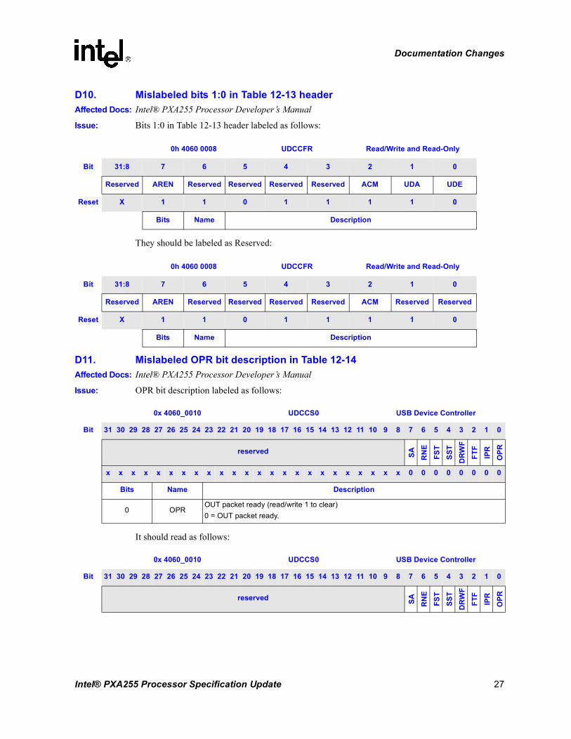
Documentation Changes
D10. Mislabeled bits 1:0 in Table 12-13 headerAffected Docs: Intel® PXA255 Processor Developer’s Manual
Issue: Bits 1:0 in Table 12-13 header labeled as follows:
They should be labeled as Reserved:
D11. Mislabeled OPR bit description in Table 12-14Affected Docs: Intel® PXA255 Processor Developer’s Manual
Issue: OPR bit description labeled as follows:
It should read as follows:
0h 4060 0008 UDCCFR Read/Write and Read-Only
Bit 31:8 7 6 5 4 3 2 1 0
Reserved AREN Reserved Reserved Reserved Reserved ACM UDA UDE
Reset X 1 1 0 1 1 1 1 0
Bits Name Description
0h 4060 0008 UDCCFR Read/Write and Read-Only
Bit 31:8 7 6 5 4 3 2 1 0
Reserved AREN Reserved Reserved Reserved Reserved ACM Reserved Reserved
Reset X 1 1 0 1 1 1 1 0
Bits Name Description
0x 4060_0010 UDCCS0 USB Device Controller
Bit 31 30 29 28 27 26 25 24 23 22 21 20 19 18 17 16 15 14 13 12 11 10 9 8 7 6 5 4 3 2 1 0
reserved SA RN
EFS
TSS
TD
RW
FFT
FIP
RO
PR
x x x x x x x x x x x x x x x x x x x x x x x x 0 0 0 0 0 0 0 0
Bits Name Description
0 OPROUT packet ready (read/write 1 to clear)0 = OUT packet ready.
0x 4060_0010 UDCCS0 USB Device Controller
Bit 31 30 29 28 27 26 25 24 23 22 21 20 19 18 17 16 15 14 13 12 11 10 9 8 7 6 5 4 3 2 1 0
reserved SA RN
EFS
TSS
TD
RW
FFT
FIP
RO
PR
Intel® PXA255 Processor Specification Update 27

Documentation Changes
D12. The reset bits for Table 12-13 UDC Control Function Register were numbered incorrectly.
Affected Docs: Intel® PXA255 Processor Developer’s Manual
Issue: Table 12-13 used to read:
It now reads:
x x x x x x x x x x x x x x x x x x x x x x x x 0 0 0 0 0 0 0 0
Bits Name Description
0 OPROUT packet ready (read/write 1 to clear)1 = OUT packet ready.
0h 4060 0008 UDCCFR Read/Write and Read-Only
Bit 31:8 7 6 5 4 3 2 1 0
Reserved AREN Reserved Reserved Reserved Reserved ACM UDA UDE
Reset X 1 1 0 1 1 1 1 0
Bits Name Description
31:8 — Reserved – Read as unknown and must be written as zero.
7 AREN
ACK RESPONSE ENABLE (read/write 1 to set)0 – Send NAK response to SET_CONFIGURATION and
SET_INTERFACE commands1 – Send ACK response to SET_CONFIGURATION and
SET_INTERFACE commands
6 — Reserved – Read as unknown and must be written as zero.
5 — Reserved – Read as unknown and must be written as zero.
4 — Reserved – Read as unknown and must be written as zero.
3 — Reserved – Read as unknown and must be written as zero.
2 ACM
ACK CONTROL MODE (read/write 1 to set)0 – Send ACK response to SET_CONFIGURATION and
SET_INTERFACE commands with no user intervention 1 – Send NAK response to SET_CONFIGURATION and
SET_INTERFACE commands until UDCCFR[AREN] = 1
1 — 1 – Reserved – Read as unknown and must be written as zero.
0 — 1 – Reserved – Read as unknown and must be written as zero.
28 Intel® PXA255 Processor Specification Update

Documentation Changes
D13. Mislabeled RSP bit description in Table 12-18Affected Docs: Intel® PXA255 Processor Developers Manual
Issue: RSP bit description labeled as follows:
0h 4060 0008 UDCCFR Read/Write and Read-Only
Bit 31:8 7 6 5 4 3 2 1 0
Reserved AREN Reserved Reserved Reserved Reserved ACM Reserved Reserved
Reset X 0 1 1 1 1 0 1 0
Bits Name Description
31:8 — Reserved – Read as unknown and must be written as zero.
7 AREN
ACK RESPONSE ENABLE (read/write 1 to set)0 – Send NAK response to SET_CONFIGURATION and
SET_INTERFACE commands1 – Send ACK response to SET_CONFIGURATION and
SET_INTERFACE commands
6 — Reserved – Read as unknown and must be written as zero.
5 — Reserved – Read as unknown and must be written as zero.
4 — Reserved – Read as unknown and must be written as zero.
3 — Reserved – Read as unknown and must be written as zero.
2 ACM
ACK CONTROL MODE (read/write 1 to set)0 – Send ACK response to SET_CONFIGURATION and
SET_INTERFACE commands with no user intervention (B-step default)
1 – Send NAK response to SET_CONFIGURATION and SET_INTERFACE commands until UDCCFR[AREN] = 1
1 — 1 – Reserved – Read as unknown and must be written as zero.
0 — 1 – Reserved – Read as unknown and must be written as zero.
0x 4060_00200x 4060_00340x4060_0048
UDCCS4UDCCS9
UDCCS14USB Device Controller
Bit 31 30 29 28 27 26 25 24 23 22 21 20 19 18 17 16 15 14 13 12 11 10 9 8 7 6 5 4 3 2 1 0
reserved
RSP
RN
E
rese
rved
DM
ER
OF
RPC RFS
Reset x x x x x x x x x x x x x x x x x x x x x x x x 0 0 0 0 0 0 0 0
Bits Name Description
7 RSPReceive short packet (read-only)0 = Short packet received and ready for reading.
Intel® PXA255 Processor Specification Update 29

Documentation Changes
It should read:
D14. Replaced Table 12-13.Affected Docs: Intel® PXA255 Processor Developer’s Manual
Issue: Table 12-13 used to read:
It now reads:
0x 4060_00200x 4060_00340x4060_0048
UDCCS4UDCCS9UDCCS14
USB Device Controller
Bit 31 30 29 28 27 26 25 24 23 22 21 20 19 18 17 16 15 14 13 12 11 10 9 8 7 6 5 4 3 2 1 0
reserved
RSP
RN
E
rese
rved
DM
ER
OF
RPC RFS
Reset x x x x x x x x x x x x x x x x x x x x x x x x 0 0 0 0 0 0 0 0
Bits Name Description
7 RSP Receive short packet (read-only)1 = Short packet received and ready for reading.
Table 12-13. UDC Control Function Register
0h 4060 0008 UDCCFR Read/Write and Read-Only
Bit 31:8 7 6 5 4 3 2 1 0
Reserved AREN Reserved Reserved Reserved Reserved ACM Reserved Reserved
Reset X 0 1 1 1 1 0 1 0
Bits Name Description
31:8 — Reserved – Read as unknown and must be written as zero.
7 AREN
ACK RESPONSE ENABLE (read/write 1 to set)0 – Send NAK response to SET_CONFIGURATION and
SET_INTERFACE commands1 – Send ACK response to SET_CONFIGURATION and
SET_INTERFACE commands
6 — Reserved – Read as unknown and must be written as zero.
5 — Reserved – Read as unknown and must be written as zero.
4 — Reserved – Read as unknown and must be written as zero.
3 — Reserved – Read as unknown and must be written as zero.
2 ACM
ACK CONTROL MODE (read/write 1 to set)0 – Send ACK response to SET_CONFIGURATION and
SET_INTERFACE commands with no user intervention (B-step default)
1 – Send NAK response to SET_CONFIGURATION and SET_INTERFACE commands until UDCCFR[AREN] = 1
1 — 1 – Reserved – Read as unknown and must be written as zero.
0 — 1 – Reserved – Read as unknown and must be written as zero.
30 Intel® PXA255 Processor Specification Update
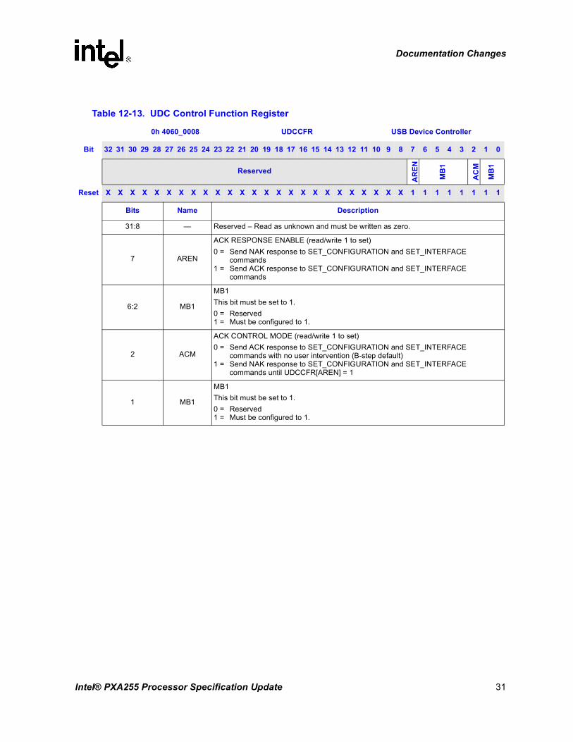
Documentation Changes
Table 12-13. UDC Control Function Register
0h 4060_0008 UDCCFR USB Device Controller
Bit 32 31 30 29 28 27 26 25 24 23 22 21 20 19 18 17 16 15 14 13 12 11 10 9 8 7 6 5 4 3 2 1 0
Reserved
AR
EN
MB
1
AC
M
MB
1
Reset X X X X X X X X X X X X X X X X X X X X X X X X X 1 1 1 1 1 1 1 1
Bits Name Description
31:8 — Reserved – Read as unknown and must be written as zero.
7 AREN
ACK RESPONSE ENABLE (read/write 1 to set)0 = Send NAK response to SET_CONFIGURATION and SET_INTERFACE
commands1 = Send ACK response to SET_CONFIGURATION and SET_INTERFACE
commands
6:2 MB1
MB1This bit must be set to 1.0 = Reserved1 = Must be configured to 1.
2 ACM
ACK CONTROL MODE (read/write 1 to set)0 = Send ACK response to SET_CONFIGURATION and SET_INTERFACE
commands with no user intervention (B-step default)1 = Send NAK response to SET_CONFIGURATION and SET_INTERFACE
commands until UDCCFR[AREN] = 1
1 MB1
MB1This bit must be set to 1.0 = Reserved1 = Must be configured to 1.
Intel® PXA255 Processor Specification Update 31

Documentation Changes
32 Intel® PXA255 Processor Specification Update