spectrally adaptive nanoscale quantum dot sensors
TRANSCRIPT

Technical article Wiley Handbook of Science and Technology for Homeland Security
Article ID: IS24 Page 1
Spectrally Adaptive Nanoscale Quantum Dot Sensors Woo-Yong Jang Biliana Paskaleva Majeed M. Hayat Sanjay Krishna Keywords Quantum Dots; Infrared Detector; DWELL; Spectral Tuning; Algorithmic Spectrometer; Feature Selection Abstract The potential use of nanotechnology for hyperspectral (HS) and multispectral (MS) sensing and imaging is described in this article. It is noted how HS and MS sensors/imagers have great potential for a variety of applications important to the intelligence community; such applications range from monitoring chemical-agent production to identifying geographical terrain. It is also noted that, by sensing the spectrum of reflectance/transmittance of the agents in different wavelength bands—as can be done with HS/MS systems— image-analysis capability and detection probability can be greatly improved. However, traditional MS/HS systems are fairly bulky and expensive. The work described concerns advances in nanotechnology that offer potential solutions to these drawbacks. In particular, the creation of spectrally adaptive focal-plane arrays, based upon nanoscale quantum dots (QDs) in the mid-infrared regime (3-14 μm), hold promise of producing compact and relatively inexpensive systems. Such sensors use electro-optics and, thus, do not involve moving parts. The spectral adaptability is mainly attributed to the quantum-confined Stark effect that results from the QDs being placed in asymmetrical quantum potential wells. As a result, QD detectors can sense information over different spectrally overlapping bands as the electrical bias applied across the detector is judiciously varied. Signal-processing based algorithms are then developed and utilized to maximally exploit the bias-dependent and diverse spectral response of the QD detectors for the purpose of target-spectrum reconstruction and target classification. Examples of these applications are also given in this article. Advances in hyperspectral (HS) and multispectral (MS) sensing and imaging in the infrared (IR) spectrum have enabled numerous remote-sensing applications.

Technical article Wiley Handbook of Science and Technology for Homeland Security
Article ID: IS24 Page 2
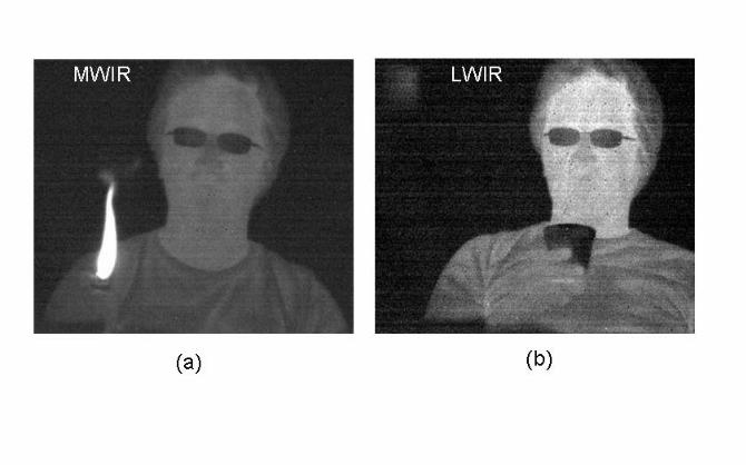
These include military surveillance (i.e., target recognition, identification and classification), medical imaging (i.e., medical diagnosis), and monitoring geographical terrain, only to name a few. Conventional HS/MS systems offer spectral information of a scene (target or an agent) in a spectral band by sensing a wide range of narrow segments of the IR spectrum in a spectral range of interest. This can be achieved by using a broadband IR detector in conjunction with dispersive optics (e.g., a bank of IR optical filters) that can be utilized to specify the spectral bands to be sensed. Alternatively, multiple sensors, each sensitive to a designated spectral range, can be employed to sense a wide spectral range. However, either one of these complex conventional methods is of relatively large physical size and high cost. Nanoscale and spectrally adaptable sensors are emerging as a highly desirable alternative to conventional MS/HS sensing strategies that feature simplicity through its single-detector nature (or array of identically fabricated detectors) without requiring dispersive elements. To this end, a new class of IR photodetectors based on nanoscale epitaxial quantum-dots(QDs) have recently been proposed and developed [1,2]. A key feature of this technology is that it exploits inter-subband transitions between quantum-confined energy levels in a self-assembled dots-in-a-well (DWELL) structure in an InAs/GaAs/AlXGa1-XAs semiconductor material system [3]. Potential advantages of this detector technology are low dark current, high operating temperature, and notably bias-controlled tunability [4]. The quantum-confined Stark effect applied to the system comprising dots in an asymmetric well, results in a bias-dependent spectral response and also introduces a red shift (spectral shift) with significant spectral overlap [5] as the bias is varied in nominal range. Hence, a single photodetector can be operated as multiple detectors simply by applying different bias: the bias-dependent photocurrents of a single detector can be regarded as the outputs, resulting from spectrally overlapping bands. Recently, DWELL-based focal plane array (FPA) grown and processed at the Center for High Technology Materials (CHTM) at the University of New Mexico had successfully demonstrated multicolor sensing capability [6] in both mid-wave infrared (MWIR) and long-wave infrared (LWIR) regions. Figure 1 shows representative imagery showing the DWELL-based FPA’s capability to sense MWIR and LWIR radiation. In order to maximally exploit the features of bias-dependent and spectrally overlapping spectra from the DWELL photodetector, two sets of signal-processing algorithms were developed and tested to further bring about the following two extended enabling functionalities that are based on post processing of data. The first is the capability for continuous spectral tuning [7-9], which enables a so-called DWELL-based algorithmic spectrometer; and the second is the capability for application-specific, optimal hyperspectral feature selection, which in turn, enables target recognition [13]. The rationale behind either one of these algorithms is to judiciously fuse multiple bias-dependent photocurrents from a single DWELL detector based on precise mathematical rules.

Technical article Wiley Handbook of Science and Technology for Homeland Security
Article ID: IS24 Page 3
In this article, we report the principles, fabrication and operation of the spectrally agile and bias-tunable DWELL photodetector. Device growth and processing are briefly reviewed, followed by results on device characterization. Device optimization for improving the DWELL’s operating temperature is also described. In addition, two key post-processing strategies for maximal data exploitation are also reviewed and analyzed: the DWELL-based algorithmic spectrometer and hyperspectral feature-selection for target recognition.
Principle of Operation for DWELL Photodetectors A DWELL detector is a smart hybrid of conventional quantum-well (QW) and QD infrared photodetectors. In a heterostructure, InAs QDs are embedded in InGaAs-GaAs multiple QWs, shown in Fig.2 [9]. Just as conventional QD detectors, a DWELL detector is inherently sensitive to normal-incidence radiation and photons. Lower dark-current levels are expected since the ground state is lowered with respect to GaAs band edge. Longer intersubband relaxation times in a DWELL structure can achieve a relatively high detectivity [11]. In addition, the reduced thermionic emission inherent in the DWELL technology leads to higher operating temperatures. Due to the quantum-confined Stark effect, a bias-dependent spectral response is evident depending upon the asymmetric electronic potential of a geometrically asymmetric DWELL structure. Two main attributes of this geometry are the shape of the dot and the different thicknesses of the QW above and below the dot, which together lead to variation of the local potential as a function of the applied bias. A DWELL detector could provide better control over the operating wavelength and nature of the allowable energy transitions (bound-to-bound, bound-to-quasi-bound and bound-to-continuum (barrier)) in Fig. 3 [9]. All the DWELL devices considered in this article were fabricated and characterized at CHTM. Brief Descriptions of Device Growth and Processing The DWELL structures were grown by V-80 molecular-beam epitaxy (MBE) system, with an As2 cracker source. An average of 2.4 monolayers of InAs dots were deposited on the sample with a rate of 0.053MLs-1. Then the dots were Si-doped at a level of 1-5x10¹⁰/cm2. The DWELL consists of 30 stacks of InAs/GaAs/AlGaAs heterostructures between two n+ GaAs contact layers. DWELL detectors were then processed using standard contact-lithography, plasma-etching, and metallization techniques in a class 100 clean-room environment. Each 400μm square n-i-n mesas with top pixel apertures, ranging from 25 to 300μm in diameter, were lithographically defined in the top metal contact [4,9]. Device Characterization Spectral response measurements were performed on single pixel InGaAs-DWELL detectors with a Nicolet 870 FTIR (Fourier Transform Infrared)

Technical article Wiley Handbook of Science and Technology for Homeland Security
Article ID: IS24 Page 4
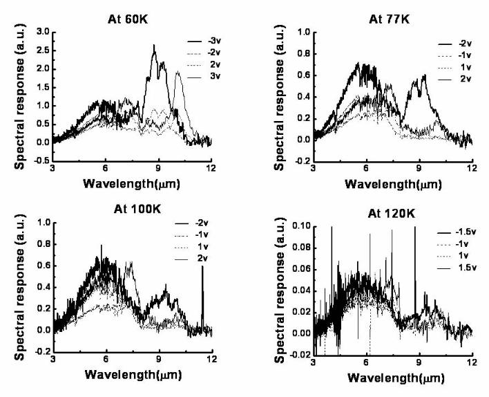
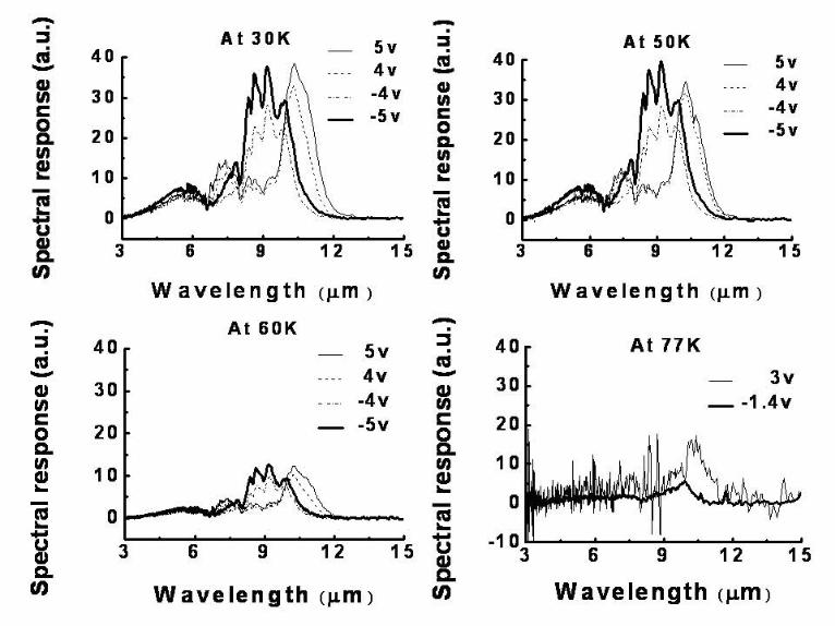
spectrometer and a Keithley 428 current-amplifier, which controls the electrical bias to the detectors. Multiple measurements of experimental photocurrents and dark currents are taken at different biases using a HP parameter analyzer. The bias-dependent spectral measurements and the corresponding experimental photocurrents of the DWELL detector are shown in Fig. 4 [9]. Due to a red shift (spectral shift), there exists two different peaks at LWIR region, one around 9.5μm with negative bias and the other at 10.5μm with positive bias. However, the drawback of the current DWELL is the limited operating temperature because of the dominance of the dark-current at higher device temperatures [9]. In Fig. 5 [9], the spectral response of the DWELL starts degrading remarkably as the operating temperature of the device exceeds 60K. Also the working range of applied bias becomes narrower. Especially at 77K, it is to be noted that no spectral variation is observed for the applied bias range. More details of the characterization can be found in [9]. Higher Operating Temperature DWELL (“Double DWELL”) Higher temperature operation is most crucial to reduce device size and cost since the required cooling system is bulky and expensive. By achieving up to near-room temperature levels, this DWELL photodetector can be more effective due to its tunability as compared to the current state of art detectors. To further increase the operating temperature, the present InAs quantum dots/InGaAs/GaAs/AlGaAs DWELL growth structure is further modified by the increase in the shoulder of the GaAs well and the addition of shoulders on both sides of the InGaAs well, so it becomes the complete double DWELL (DDWELL) structure. The optimizations of the growth procedure and the processing technique can potentially lower the dark current level to obtain higher operating temperature of the device. In Fig.6 [11,12], the bias-dependent DDWELL spectral response is observed until the device temperature of 120K and the spectral shift are still present in LWIR. However, at 120K, the device photocurrent is dominated by noise mainly due to the high dark current level.
Description of the DWELL-based Algorithmic Spectrometer The concept of the spectral-tuning algorithm in conjunction with the DWELL-based detector is thoroughly reviewed here to describe the role of algorithmic spectrometer, drawing freely from our earlier published works [7,8]. Assume that the object (target) of interest is illuminated by a black-body broadband radiation source and a DWELL detector probes the illuminated object applying different electrical biases, producing a group of bias-dependent photocurrents. The goal is to exploit these bias-dependent photocurrents to estimate (approximately reconstruct) the spectrum of the object of interest without the utilization of any physical dispersive optics or a spectrometer. The spectral estimation procedure is described as follows. First, a series of hypothetical, narrowband tuning filters, each with a prescribed center wavelength and transmittance, are defined by
Technical article Wiley Handbook of Science and Technology for Homeland Security
Article ID: IS24 Page 5
sweeping across the desired center wavelength of narrowband tuning filter in a spectral region of interest. Second, a set of superposition weights are calculated by estimating the spectrum of a DWELL detector with the choice of the tuning filters. Third, for each defined filter, the spectral reconstruction of object is performed by forming a weighted superposition of the DWELL spectral responses with pre-determined superposition weights. With this step completed, the so-called “synthesized photocurrent”, defined as the target reconstruction with weights, is shown to best approximate the ideal photocurrent obtained by sensing the same object of interest using an ideal broadband (with a spectrally flat response) detector looking at the object through the spectral tuning filter. This approximation results in the minimization of the mean-square-error (MSE) between the synthesized photocurrent and the ideal response. Finally, the third step is repeated for every tuning wavelength and the spectrum is reconstructed within the prescribed wavelength range. In Fig. 7 [9], the conventional spectrometer with an ideal broadband IR detector and a group of optical IR filters is schematically compared with the proposed algorithmic spectrometer for describing their functional equivalence. Mathematical Description
Mathematically, the reconstructed target spectrum ∧
nI λ (Eq. (1) in [9]) at a
desired tuning wavelength nλ , is formulated as
.ΙwI i
K
iinn ∑
=
∧
=1
,λ (1)
The weight vector, wn = [wn,1 , …, wn,K]T, is determined by computing the expression (Eq. (18) in [8])
wn =[ATA + Φ + αQTATAQ]-1[ATnλr ], (2)
where A = a set of spectral responses of DWELL = [R1,…, RK] and each
Tkkk RR )](,),([ maxmin λλ …=R ranging from a minimum value of minλ to a maximum
value of maxλ . In addition, the Φ is a diagonal noise-equivalent matrix whose kth diagonal entry is Rk
T Rk/SNRk2, where SNRk represents the signal-to-noise ratio
determined by the following formula (Eq. (3) in [9]),
SNRk = yp,k/σN,k, (3) where yp,k is the experimentally averaged photocurrent (over 100 realizations) and σN,k is the standard deviation of the dark current, also calculated empirically from the dark-current realizations. Then the remaining term named the

Technical article Wiley Handbook of Science and Technology for Homeland Security
Article ID: IS24 Page 6
regularization term, αQTATAQ, limits spurious fluctuations in the approximation, where Q and α are the Laplacian operator and the regularization weight respectively.
Experimental Demonstration of Algorithmic Spectrometer Here we review an experimental application of the DWELL-based algorithmic spectrometer drawing from our earlier work reported in [9]. Arbitrarily chosen targets in the LWIR region are considered and examined. First the spectral responses of the DWELL photodetector were measured at different biases varied between -5V and 5V at a temperature of 30K. Then the corresponding experimental photocurrent and dark current are obtained by illuminating the LWIR target with the FTIR source at each bias. As described in earlier section, measured spectral responses of the DWELL photodetector in conjunction with hypothetical, narrowband tuning filters, determine the superposition weights in a spectral region of interest. Then the experimentally obtained photocurrents are synthesized to give the weighted superposition representing each reconstructed point of the target at a desired tuning wavelength. The reconstruction results for four different target spectra, shown in Fig. 8, are obtained by continuously tuning from 2.55μm to 12.5μm in steps of 0.05μm. The solid curve is the true spectrum of target sensed by the standard broadband detector; whereas the dotted curve is the experimental reconstruction of algorithmic spectrometer incorporated with DWELL photodetector. The comparison of these two spectra clarifies the validation of algorithmic spectrometer. However, one limitation is evident, that since the DWELL detector lacks its spectral information beyond 11.5μm, the algorithmic spectrometer does not accurately reconstruct the long wavelength edge of target f2(λ) in Fig. 8(b).
Refining the Algorithmic Spectrometer: Reduction of required biases and Higher Operating Temperatures In an actual system, however, it may not be practical to use a large number of biases for operating the algorithmic spectrometer due to device limitations and the computational inefficiency as described next. Device limitations are related to the operation of the DWELL photodetector in that a reduction in the operating range of the bias is seen at high operating temperatures. With less biases required by the tuning algorithm, the implementation of the algorithmic spectrometer simplifies, leading to increased speed, which may be suitable for near real-time applications. To this end, the algorithmic spectrometer is further refined by introducing the bias-selection scheme to reduce the number of required biases for acceptable target reconstruction. Bias-selection [12] is performed as follows: first, we find the threshold for the superposition weights, which can be pre-determined from the analysis of the ordinary algorithmic spectrometer. Dominant weights are then selected while others are discarded based on the threshold.

Technical article Wiley Handbook of Science and Technology for Homeland Security
Article ID: IS24 Page 7
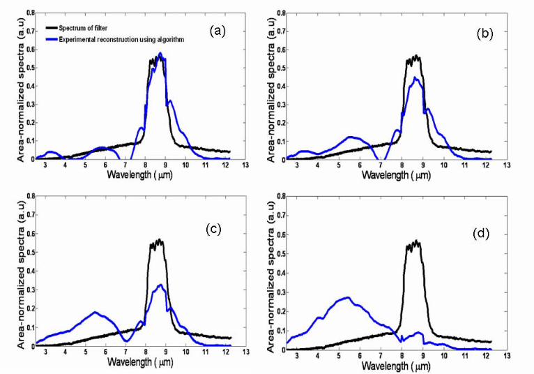
Also, the DDWELL-based detector described earlier is used with this enhanced algorithmic spectrometer to test the performance against the detector operating temperature. Here we first measured the spectral responses of DDWELL detector for 30 biases available in range between -5V and 5V. The spectral measurement was repeated for different operating temperatures from 60K to 120K. As illustrated in Fig. 6, the operating bias range at 120K is significantly reduced by the increase in device temperature, causing larger dark currents. Then one of LWIR targets described in Fig. 8 was tested for a reconstruction using the algorithmic spectrometer with reduced number of biases; the minimum 10 biases originally from 30 biases were determined and required for achieving the reasonable target reconstruction. This algorithmic target reconstruction was repeated for incremental DDWELL operating temperatures (60K, 77K, 100K and 120K). The results shown in Fig. 9 are generally good at the device temperatures 60K and 77K, yet at 100K or above, the performance of algorithmic spectrometer is significantly degraded due to the lack of spectral information available from the DDWELL detector.
Canonical Correlation Feature Selection Algorithm and its Application to DWELL Detectors Owing to the capability to tune the QDIP responsivity continuously in its central wavelength and shape with the applied bias voltage, a single QDIP can be exploited as a multispectral or even hyperspectral IR sensor [8, 13]; the photocurrents measured at different operational biases can be viewed as outputs of different spectral bands. Unlike more traditional sensors, the spectral responsivities of QDIPs are broad (~1 micron) and overlapping, thereby producing a high level of redundancy at the output photocurrents. Furthermore, the noise level at the photocurrents also varies continuously depending upon the bias applied, yielding band-dependent SNR. These attributes of QDIP sensors necessitate the development of alternative methods for spectral feature-selection that will enable more efficient utilization of such sensors [13]. A novel, problem-specific spectral feature-selection algorithm termed the Canonical Correlation Feature Selection (CCFS) was rigorously developed for a general class of multispectral/hyperspectral sensors whose bands are both overlapping and noisy [13]. The approach is based upon minimum mean-square-error (MMSE) criterion in conjunction with a canonical correlation (CC) analysis framework. The criterion ranks the best linear combinations of noisy and overlapping bands, termed superposition bands, guaranteeing minimal distances between each of the centers of the classes and their reconstructions in the space spanned by the sensor’s bands [13]. In particular, for a given spectral pattern p ,
the algorithm selects an optimal superposition band, ∑=
=k
iii faf
1
, represented by
Technical article Wiley Handbook of Science and Technology for Homeland Security
Article ID: IS24 Page 8
the weight vector ( )Tkaa ,,1
* …=a , defined as solution of the constrained minimization problem
( )⎥⎥⎦
⎤
⎢⎢⎣
⎡+−= ∑∑
= ==∈
2
1 11,
* ,minargk
i
k
jjiiji
fRfNfpaapE
Kaa , (4)
where iN is the i th noise component associated with the sensor band if . The quantity
( ) ∑∑==
=+=k
iii
k
iiii IaNfpaI
11
~, (5)
is termed a superposition photocurrent, and it can be interpret as the output photocurrent of the superposition band f . Moreover, the superposition photocurrent can be viewed as the optimal in a MMSE sense single spectral feature that can represent the spectral pattern p in the space spanned by the sensor bands in the presence of noise. The concept of optimal superposition band and photocurrent presented in (4) is then extended to a canonical feature-selection algorithm by utilizing the idea of the CC analysis [13]. Based on a computed sequence of principal angles
kθ between any two finite-dimensional Euclidean spaces, U and V, the CC analysis yields the so-called CC coefficients, ( )kk θρ cos= , between the two spaces. The first CC coefficient is computed as j
Tijivu
,1 max=ρ , where vectors
mii ,,1, …=u and nii ,,1, …=v are unit length vectors that span the two spaces respectively [13]. The two vectors for which the maximum is attained are then removed, and 2ρ is computed from the reduced sets of the bases. This process is repeated until one of the remaining subspaces becomes empty. When the inner product between two vectors is perturbed by additive noise as in the case of the photocurrent seen in (5), the CC analysis approach cannot be applied directly. A stochastic version of “principal angle” is introduced in (4) and used for ordering and selection of the optimal spectral features. The superposition-band selection procedure described by (4) is repeated sequentially as many times as the number of the classes of interest, producing a canonical set of superposition bands. Following the general principle of CC analysis, at each stage, the algorithm excludes the class that has been selected in the prior stage from the search for the optimal direction and every superposition band is selected from a subspace of the sensor space that is in the orthogonal complement of the previously selected superposition direction. Application of the CCFS algorithm to the problem of separability and classification analysis of seven rock classes [13] has demonstrated the efficacy of the proposed approach in a challenging remote sensing task. A number of
Technical article Wiley Handbook of Science and Technology for Homeland Security
Article ID: IS24 Page 9
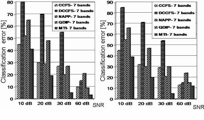
spectra of common rock samples in different grain size were selected from the Advanced Spaceborne Thermal Emission and Reflection Radiometer (ASTER) hyperspectral database to create training and two testing data sets. To extend the training and testing data sets, the endmebers in each rock-class were perturbed with different mixing materials, using a simple two-component linear mixing model [13]. QDIP spectral responses measured at different biases voltages varied in the range -4.2V to 2.6V and at a temperature of 30K were used to simulate the operation of a single-pixel, multispectral DWELL sensor. In the presence of noise, for different SNR cases (10dB, 20dB, 30dB and 60dB) and using Bayesian classifier, the separability and classification results for the CCFS algorithm were compared with four different feature-selection strategies, each using seven spectral features. Here the number of selected superposition features is determined by number of classes of interest – seven. The first strategy was termed deterministic CCFS (DCCFS) and it employs the proposed CC feature-selection but without accounting for the photocurrent noise during the feature-selection process. In the second case, termed noise-adjusted projection pursuit (NAPP), seven features were extracted using the NAPP algorithm. The last two cases correspond to the classifiers that use seven QDIP and seven Multispectral Thermal Imager (MTI) bands. From the results presented in Fig. 10, right and left, we can conclude that embedding the noise statistics in the canonical feature-selection leads to a significant improvement in the classification. For the first three SNR cases (Fig. 10, right and left,) the CCFS algorithm performs almost twice as good as the DCCFS algorithm. In the limiting case of a very high SNR, the performance of the CCFS and DCCFS algorithms becomes almost identical, as expected, and the classification error drops to 10-15%. Comparison with the NAPP algorithm, as seen in Fig. 10, shows that the CCFS algorithm outperforms the NAPP technique in the cases of low (10dB) and high (60dB) SNRs confirming further that CCFS offers enhanced robustness with respect to the photocurrent noise. These results indicate a great potential for operating QDIP sensors at higher temperatures, in the range 50K-70K, and thus leading to remote sensing instruments with reduced size and cost.
Technical article Wiley Handbook of Science and Technology for Homeland Security
Article ID: IS24 Page 10
References [1] Raghavan, S, Rotella, P, Stintz, A, Fuchs, B, Krishna, S, Morath, C, Cardimona, DA and Kennerly, SW. High responsivity, normal-incidence long-wave infrared (l; 7.2 mm) InAs/In0.15Ga0.85As dots-in-a-well detector. Appl. Phys. Lett. 2002 Vol. 81:1369–1371.
[2] Phillips, J, Bhattacharya, P, Kennerly, SW, Beekman, DW and Dutta, M. Self-assembled InAs-GaAs quantum-dot inter-subband detectors. IEEE J. Quant. Elect. 1999 Vol. 35:936–942.
[3] Krishna, S. InAs/InGaAs Quantum Dots in a Well Photodetectors. J. Phys. D(Appl. Phys.). 2005 Vol. 38:2142–2150.
[4] Krishna, S, Rotella, P, Raghavan, S, Stintz, A, Hayat, MM, Tyo, SJ and Kennerly, SW. 2002. Bias-dependent tunable response of normal incidence long wave infrared quantum dot detectors. Proc. of IEEE/LEOS Annu. Meeting. Vol. 2: 754–755.
[5] Krishna, S, Hayat, MM, Tyo, JS, Raghavan, S and Sakoğlu, Ü. Detector with tunable spectral response. 2007 United States Patent No. 7, 217,951.
[6] Varley, ES, Lenz, M, Lee, SJ, Brown, JS, Ramirez, DA, Stintz, A, Krishna, S, Reisinger, A and Sundaram, M. Single bump,two-color quantum dot camera. Appl. Phys. Lett. 2007 Vol. 91. [7] Sakoğlu, Ü, Tyo, JS, Hayat, MM, Raghavan, S and Krishna, S. Spectrally adaptive infrared photodetectors using bias-tunable quantum dots. J. Opt. Soc. Am. B. 2004 Vol. 21:7–17.
[8] Sakoğlu, Ü, Hayat, MM, Tyo, JS, Dowd, P, Annamalai, S, Posani, KT and Krishna, S. A statistical method for adaptive sensing using detectors with spectrally overlapping bands. Appl. Opt. 2006 Vol. 45:7224 – 7234.
[9] Jang, W-Y, Hayat, MM, Tyo, JS, Attaluri, RS, Vandervelde, TE, Sharma, YD, Shenoi, R, Stintz, A, Cantwell, ER, Bender, S and Krishna, S. Demonstration of Bias Controlled Algorithmic Tuning of Quantum Dots in a Well Mid-infrared Detectors. Submitted to IEEE J. Quant. Elect. 2008. [10] Matthews, MR, Steed, RJ, Frogley, MD, Phillips, CC, Attaluri, RS and Krishna, S. Transient photoconductivity measurements of carrier lifetimes in an InAs/In0.15Ga0.85As dots-in-a-well detector. Appl. Phys. Lett. 2007 Vol. 90. [11] Vandervelde, TE, Lenz, MC, Varley, E, Barve, A, Shao, J, Shenoi, R, Ramirez, DA, Jang, W-Y, Sharma, YD and Krishna, S. Quantum Dots-in-a-Well Infrared Photodetectors. SPIE Defense and Security Symposium. March 16-20, Orlando, Florida, 2008.

Technical article Wiley Handbook of Science and Technology for Homeland Security
Article ID: IS24 Page 11
[12] Jang, W-Y, Hayat, MM, Bender, S, Sharma, YD, Shao, J and Krishna, S. Performance enhancement of an algorithmic spectrometer with Quantum-Dots-in-a-Well Infrared Detectors. International Symposium on Spectral Sensing Research, June 23-27, Hoboken, New Jersey, 2008.
[13] Paskaleva, B, Hayat, MM, Wang, Z, Tyo, S and Krishna, S. Canonical Correlation Feature Selection for Sensors with Overlapping Bands:Theory and Application. IEEE Trans. Geosci. & Remote Sens. 2008, in press.
Further reading list [1] Rogalski, A. Assessment of HgCdTe photodiodes and quantum well infrared photoconductors for long wavelength focal plane arrays. Infrared Phys. Technol. 1999 Vol. 40:279–294. [2] Levine, BF. Quantum-well infrared photodetectors. J. Appl. Phys. 1993 Vol. 74:1–81.
Cross-references Enter your cross-references here. Please select up to five cross-references. These are related articles in the Handbook that will form valuable “see also” links for the reader. You should choose your cross-references from the conceptual outline supplied with your invitation.
Glossary terms Quantum Dots, Nanoscale Sensors, Spectrally Adaptive, Post processing Algorithms.
Suggested reviewers Professor Chennupati Jagadish Federation Fellow Department of Electronic Materials Engineering Research School of Physical Sciences and Engineering Australian National University, Canberra, ACT 0200, AUSTRALIA Ph: 61-2-6125-0363, FAX: 61-2-6125-0511, Email: [email protected] Email: [email protected] Dr. A. G. U. Perera Professor of Physics Department of Physics & Astronomy Georgia State University Atlanta, GA 30303. tel: 404 413 6037 (office) e-mail:[email protected]
Technical article Wiley Handbook of Science and Technology for Homeland Security
Article ID: IS24 Page 12
Prof. John P.R. David Department of Electronic & Electrical Engineering University of Sheffield, Sir Frederick Mappin Building Mappin Street Sheffield S1 3JD, U.K. Tel:44-(0)114-2225185, Fax:44-(0)114-2225143 [email protected] Figure legends
Figure 1 Two-color images of a DWELL-based FPA in (a) MWIR (3~5 μm) and (b) LWIR (8~12 μm).
Figure 2 General schematic of the DWELL heterostructure (top,left), example of the DWELL growth schematic (middle) and cross-sectional transmission electron microscopy (TEM) image (right) (Adapted from Fig.1 in ref. [9]).
Figure 3 DWELL energy band diagram describing: (1) bound-to-bound, (2) bound-to-quasi-bound, and (3) bound-to-continuum transitions (Adapted from Fig.2 in ref. [9]).
Figure 4 Bias-dependent spectral responses of DWELL detector (left) and its photocurrent characteristic (right) (Adapted from Fig.6 in ref. [9]).
Figure 5 Bias-dependent spectral responses of DWELL detector as a function of different operating temperatures at 30K (top,left), 50K (top, right), 60K (bottom,left), and 77K (bottom,right) (Adapted from Fig.7 in ref. [9]).
Figure 6 Bias-dependent spectral responses of DDWELL detector as a function of different operating temperatures at 60K (top,left), 77K (top, right), 100K (bottom,left), and 120K (bottom,right) (Adapted from ref. [11,12]).
Figure 7 (a) A conventional spectral sensing method using a standard broadband IR detector and a family of optical IR filters. (b)The proposed algorithmic-spectrometer equivalent of (a). Initially, several photocurrents (of the target spectrum f) are taken at different bias voltages v1 … vk. Then, the measured responses at each bias are algebraically combined with pre-determined weights wi,n that are used to match a desired filter centered at wavelength n. By changing the weights, the effect of different desired filters (similar to the ones used in (a)) is synthesized, albeit, without the use of any optical filters (Adapted from Fig.10 in ref. [9]).
Figure 8

Technical article Wiley Handbook of Science and Technology for Homeland Security
Article ID: IS24 Page 13
Experimental reconstructions using algorithmic spectrometer incorporated with DWELL detector. Solid curves represent the actual responses of the targets and the dotted curves represent the reconstructed spectra using tuning algorithm (Adapted from Fig. 13 in ref. [9]). Figure 9
Experimental reconstructions of a LWIR target using algorithmic spectrometer incorporated with DDWELL detector. Black curve represents the actual spectrum of the target and blue curves represent the reconstructed spectra with reduced biases (i.e. 10 biases) at different detector operating temperatures (a) 60K, (b) 77K, (c) 100K and (d) 120K (Adapted from ref. [12]). Figure 10 Comparison in rock-type separation for CCFS, DCCFS, noise adjusted PP, QDIP bands and MTI bands in presence of noise with average SNR values of 10, 20, 30 and 60dB. Left: Test Set-1. Right: Test Set-2 (Adapted from Fig. 5 in ref. [13]).