speed light sb-24 - xs4all klantenservice
TRANSCRIPT

Speed light
SB-24
REPAIR MANUAL
f~ :f1I! m ~
IFSA02401 - R.3244.A
... ,~•~on 1
NIKON coRPORATION ... J ft~ Tokyo. Japan
© Copyright I 988 ALL RIGHTS RESERVED ~Wffiti ~-T -~'

(
I FSA02401-R.3244.A
I. SPECIFICATIONS
1. Guide number (m, ISO 100)
Manual mode Manual repeat
Ml /1 Ml /2 Ml /4 Ml /8 Ml /16 MRl /8 MRl/16
Tl 50+5.5 36+9.9 25+6. 9 18+4. 9 12.5~~:; 18+4.9 12.5~;:; 85mm -8.0 -7.8 -5.4 -3.8 -4.8
T2 4 7+5. 1 33 +9. 1 23+6.3 16.s~j:~ 11.S~~:; 16.s~i:~ 11.5~;:~ 70mm -7. 5 -7. 1 -4.9
s 42 +4. 6· 30+8.2 21+5.8 15+4. 1 10.5~;:; 15 +4. 1 10.5~;:~ 50mm -6.7 -6.5 -4.5 -3. 2 -4.0
N 36+3.9 25+6.8 18+4. 9 12.5~~:; +2.5 12.s~;:j +2.5 35mm -5.7 -5.4 -3.9 9_ 1. 9 9-2.4
Wt 32+3.5 22+6. 0 16+4.4 11+3.0 8+2.2 11+3.0 8+2.2 28mm -5. 1 -4.7 -3.4 -2.3 -1. 7 -2.9 -2. 1
W2 30+3 . 3 21+5.8 15+4. 1 10.5~~:~ 7 5+2. 1 10.5~;:~ 7 5+2.1 24mm -4.8 -4.5 -3.2 . -1. 6 . -2.0
2. Angle of flash coverage
Flash head Angle of flash coverage Usable lenses position
W2 (24nnn) Vertically 60° Horizontally 78 ° 24nnn
Wl (28mm) 53° 70° 28nun -- ----·-N (35nnn) 45° 60° 35nnn
s (50rnm) 34 ° 46° 50mm
Tl (70mm) 26° 36° 70mrn ----,__
T2 (85mm) 23° 31° 85nun
3. Ntunber of flashes/Recycling time (At manual 1/1 setting)
No. of flashes Recycling time
AA alkaline-manganese batteries 100 or more 7 sec or shorter
AA Ni-Cd battery 40 or more 5 sec or shorter
When external power source is used:
SJ?-6 Recycling time 3 sec 30 sec
No. of flashes 250 or more 500 or more
SD-7 Recycling time 6 sec 10 sec 30 sec
No. of flashes 200 or more 300 or more 400 or more
* Autofocus illuminator and display panel illurninator are to be off and zooming operation is not to be made.
* When the external power source is used, install four alkaline-manganese batteries in the SB-24 and a 315V layer built cell in SD-6 or A-type Alkaline-manganese batteries in SD-7.
I FSA02401-R.3244.A
4. Flash mode
The following flash mode can be selected:
(1) TTL flash mode (TTL) TTL auto flash control is possible.
(2) Manual repeating flash mode (MR) Flash fires repeatedly at the fixed amount of light (1/8 or 1/16).
(3) Manual flash mode (M) Flash fires at the fixed amount of light (1/1, 1/2, 1/4, 1/8 or 1/16).
(4) Auto flash control mode (A) Flash is controlled at the aperture f/2, f/2.8, f/4, f/5.6, f/8 and f/11. (ISO 100)
4-1. TTL auto exposure control range Film speed: ISO 25 - 400 (FA, FE2, FG, F-401 or Nikonos V with sync
cord for land use) ISO 25 - 1000 (F-301, F-501, F-801)
Aperture f/1.4 - f/32 Distance 0.6 - 20m (Refer to the table in the page 4.)
4-2. Manual repeating flash
4-3.
Frequency: 1, 2, 3, 4, 5, 6, 7, 8, 9, 10 (Hz) Number of flashes:
At Ml/8 setting: 1, 2, 3, 4, 10 (Displays -- at 10 setting) At Ml/16 setting: 1, 2, 3, 4, 5, 6, 7, 8, 20
(Displays -- at 20 setting) With the built-in batteries, repeating flash is available up to 4 times at Ml/8 setting or 8 times at Ml/16 setting (with fresh batteries). The number of flashes is increased by using an external power source (SD-6, SD-7).
Synchronization with motordrive
Power Light output Sync speed Max. No. of source (Frame/sec) flashes
---- -------
Ml/16 Slower than 6 Approx. 8 Built-in Slower than 3.3 Approx. 10 batteries Slower than 6 Approx. 4 Ml /8 Slower than 3.3 Approx. 5
Built-in Ml I 16
Slower than 6 Approx. 20 batteries Slower than 3.3 Approx. 40 plus
Slower than 6 Approx. 6 SD-6 Ml /8 Slower than 3.3 Approx. 20
Biult-in Ml I 16 Slower than 6 Approx. 10
batteries Slower than 3.3 Approx. 30 plus
Slower than 6 Approx. 5 SD-7 Ml /8 Slower than 3.3 Approx. 9
Built-in battereies: AA alkaline batteries SD-6: 315V layer built cell SD-7: A-type alkaline batteries
2
c·

I FSA02401-R.3244.A
4-4. Automatic exposure control range Distance: 0.6 - 20m
ISO F No.
6, 8 1.4 2 2.8
10, 12, 16 1.4 2 2.8 4
20, 25, 32 1.4 2 2.8 4 5.6
40, 50, 64 1.4 2 2.8 4 5.6 8
80, 100, 125 2 2.8 4 5.6 8 1 1
160, 200, 250 2.8 4 5.6 8 1 1 16
320, 400, 500 4 5.6 8 1 1 16 22
640, 800, 1000 5.6 8 1 1 16 22 32
1250, 1600, 2000 8 l 1 16 22 32
2500, 3200, 4000 11 16 22 32
5000, 6400 16 22 32
5. Bounce flash
Bounce angle
Vertically: Down to -7° or up to 90° (Click stop at -7'!. 45°, 60°, 75° and 90°)
Horizontally: 90° clockwise and 180° counterclockwise (Click stop at 30 °' 60°, 90 °' 120°, 150° and 180°)
Flash head can be locked at the front position for both vertical and horizontal position.
6. Switches
Name Type Mode Function
( a Power SW Slide OFF-STBY-ON To turn on/off power, To set Standby mode
b Flash mode Slide A-M-MR-TTL To switch flabs mode selector
c Sync mode Slide NORMAL- REAR To switch sync mode selector
d ZOOM SW Push To shift zoom setting
e Open-flash Push To trigger flash, To turn on SW power in STBY mode I
I
f Adjustment Push To adjust F No., exposure SW (UP) compensation or repeating flash
frequency
g Adjsutment Push To adjsut F No., exposure SW (DOWN) compensation or repeating flash
number
h MSW To change light amount in M mode, To switch TTL1/TTL2
i Illuminator Push To light up illuminator SW
3 -

J
k
SELECT SW
m-ft SW
Push
Slide m-ft
I FSA02401-R.3244.A
To switch UP/DOWN SW input
To select indication (meters or feet)
Usable apertures/shooting distance range in TTL mode (m) (Shaded portion: A mode)
Shoo ti nc distance range (II)
1600 BOO 400 200 100 50 25 W • 241111 w. 28a11 N 35.. s so. T1 70.. Ta SS-2 1.4 5.2 - 20 5.7 - 20 6.4 - 20 7.5 - 20 8.4 - 20 8.9 - 20
2.8 2 1.4 3.7 - 20 4.0 - 20 4.5 - 20 5.2 - 20 5.9 - 20 6.3 - 20 4 2.8 2 1.4 2.6 - 20 2.9 - 20 3.2 - 20 3.7 - 20 4.2 - 20 4.4 - 20
2.0 - 16 2.3 - 18 2.6 - 20 3.0 - 20 3.2 - 20 1.5 - 11 1.6 - 12 1.8 - 14 2.1 - 16 2.3 - 17 1.0 - 8.0 1.2 - 9.0 1.3 - 10 1.5 - 11 1.6 - 12 0.7 - 5.6 0.8 - 6.3 1.0 - 7.4 1.1 - 8.3 1.1-8.8 0.6 - 4.0 0.6 - 4.5 0. 7 - 5.2 0.8 - 5.8 0.8 - 6.2 0.6 - 2.8 0.6 - 3.1 0.6 - 3.7 0.6 - 4.1 0.6 - 4.4
32 22 16 11 8 0.6 - 1.8 0.6 - 2.0 0.6 - 2.2 0.6 - 2.6 0.6 - 2.9 0.6 - 3.1 32 22 ie 11 o.6 - 1.3 0.6 - 1.4 0.6 - 1.5 0.6 - 1.8 0.6 - 2.0 0.6 - 2.2
32 22 16 0.6 - 0.9 0.6 - 1.0 0.6 - 1.1 0.6 - 1.3 0.6 - 1.4 0.6 - 1.5
Usable aperture/shooting distance range in TTI, mode (ft) (Shaded portion: A mode)
ISO fil• speed Shooting distance ranae (11}
1600 800 400 200 100 50 25 w. 241111 w. 28•• N as- s so- Ta 70- Ta as.. 2 1.4 17 - 66 19 - 66 21 - 66 25 - 66 28 - 66 29 - 66
2.8 2 1.4 12 - 66 14 - 66 15 - 66 17 - 66 20 - 66 21 - 66 4 2.8 2 1.4 8.6 - 66 9.3 - 66 11 - 66 12 - 66 14 - 66 15 - 66
6.1 - 49 6.6 - 52 7.4 - 59 8.6 - 66 9.7 - 66 11 -66 4.4 - 34 4. 7 - 37 5.3 - 41 6.0 - 48 6.9 - 54 7.3 - 58 3.1 - 24 3.3 - 26 3.7 - 29 4.3 - 34 4.9 - 38 5.2 - 41 2.2 - 17 2.4 - 18 2.7 - 20 3.1 - 24 3.5 - 27 3.7 - 29 2.0 - 12 2.0 - 13 2.0 - 14 2.2 - 17 2.5 - 19 2.6 - 20 2.0 - 8.7 2.0 - 9.2 2.0 - 10 2.0 - 12 2.0 - 13 2.0 - 14
32 22 16 11 8 2.0 - 6.1 2.0 - 6.5 2.0 - 7.3 2.0 - 8.6 2.0 - 9.6 2.0 - 10 32 22 16 11 2.0 - 4.3 2.0 - 4.6 2.0 - 5.2 2.0 - 6.0 2.0 - 6.8 2.0 - 7.2
32 22 16 2.0 - 3.0 2.0 - 3.3 2.0 - 3.6 2.0 - 4.3 2.0 - 4.8 2.0 - 5.1
4
r••--
c=

{
7. Display
7-1. LCD display
a
b
c
d
e-1
e-2
Name
Flash mode indicator
Distance segment
Distance (m)
Distance (ft)
ISO value
SET
e-3 ISO
f-1 Aperture indicator
f-2 F
I FSA02401-R.3244.A
Function Flash mode
To show flash mode TTL, M, MR, A
To indicate distance TTL, M, MR, A
Flash shooting distance scale TTL, M, MR, A
Flash shooting distance scale TTL, M, MR, A
To show ISO setting, To show TTL, M, A repeating flash number, To MR show repeating flash frequency MR
To indicate to input ISO value TTL, M, To indicate to input number & frequency of repeating flash
To show ISO value is to be input
TTL, M,
MR
A
A
To show aperture value TTL, M, MR, A
To show F No is to be input TTL, M, A 1--~~-+-~~~~~~~~~~~~~-+-~--~~~~
g-1 Angle of coverage indicator
To show angle of coverage TTL, M, MR, A
g-2 M (ZOOM) To show manual zooming TTL, M, MR, A
h-1 Exp. compensation To show exp. compensation TTL ----~~~~~~~-+~~~~~~~~-----!
h-2 +/- To show compensation value TTL is to be input
i Light amount indicator To show light amount in M mode M, MR
7-2. LED display Ready-light/Warning (after shooting)
7-3. Ready-light in viewfinder (displayed in viewfinder via shoe contact CRY) Ready-light/Warning (after and before shooting)
8. Warning
Ready-lights on SB-24 and in the camera viewfinder give the following warnings by blinking. (Blinking frequency; 4Hz)
TTL incapable Viewfinder TTL mode is set with
Before warning ready-light non-TTL camera.
shooting Out of ISO Viewfinder ISO setting is beyond range warning ready-light usable range for TTL
control.
After Full flash Viewfinder & Flash fires fully in shooting warning SB-24 ready- or TTL mode. (Blinks
lights for approx. 3 sec.)
5
A

Inside h;:i ttery L;.amber
FSA02401-R.3244.A
© @
§.! e-1 h-2· h-1 ./\...----, ·- .
fl1Ii!il l;~~I iii][:;--~ ~ hil11l11l11I ~--- SET .-i ,.._, ~ r-: ••••••••••••• .1=::===~ ,_, "-' ,_, "-1 H +1 o -1 -2 -3
~----- ISO l:f Lt Lf Lf z 0.6 0.8 1 1.5 2 3 4 6 9 1318 m
~-------119---~ !--+-.... 2. ·3 4 5 7-_ 10 15 20 304060.ft
-~ M o o1 g - 1 1 F: c' C• . / r:-zooM !:f El mm . L.f .L.f ·MI 8 a @" @f-20 f-1 ® ©
QzooMl)~(lsELt) (ITJ [A 0 OFF .i>TJt ON
(l:t:i-1)~ (llllillllll) l CD © @
LCD display and operational switches
- 6 -
(
(

m. tJB ..ff, ~ Pa r t s L I s -t IFSA0240 l -R. 3 2 4 4. A
mi.r..•~ ~ ~ 1 ~:H lf~*llrfa-lt ~ #A« llli 1't • :1t ~ * llU tt im• I& ~r It\. {;): Pcs. l'er Term of Q' ty per
Part No. Name Unit Assembly Fig. Delivery Remarks order v :,-;;( 1G308-006- l
1 1 lBlS0-061 6 Lens
-- - . --------- ·---- - --- - . --··· jt, JI 1K640-794
3 1 1B150-061 6 Ring
~---- - -· ----------- -- -- - ·- -- -7"D7!J 1K680-833
4 1 18150-061 /\, Block
--·--------- -.----- --· -----·----- ---·---7°D7!J 1K680-833-1
5 1 lBIS0-061 6 Block
·-· ·-· --- ----- -t&i~;t. 1K240-464
6 1 IBlS0-061 6 Spring
------- -- -·
lf~.f.,{t ~ Jr - 7' Iv 15045139 15045-140 7 1 lBlS0-061 6
Cable ---------- ----- -· ------- --- --- - ---------- - ·-. --- ··--
flUll PCB 15045-139 15700-205 8 1 lBlS0-061 6
PCB -- ---- -·--- -· --------- ------~- ---- ----- --------- -
.!f!iJJ(t; 7- ·:; 7" 150oi5-139 15100-003 9 2 JlllS0-061 6
Tip ......__..___ ----- --- ·-- --- --- -· ---- --- -- --- - - ---- -·
7-:;r. lKlOB-071 l 0 I x
Cover ------ ·-----------1-- ------
7-:;r.Of> 1Kll6-372 1 1 2 x
String ·------------ ------ -------------- ---------- ·- ------.
Jlf:T ~ - ;: :t 1v lBoi00-026 1 2 1 II 1 06 5
Sync. teninal --- ·-· ---- ------ -
L ______
- --------:;,~!JD~-;::t1v 18400-035
1 3 1 II 1 06 5 Sync. terminal
--~-------- ---- -----------· -- L----- ---·
'/J;r.~A7:tD?° 1S237-052
( 1 4 Tl796F 1 A 6 Cus loll ana I og
---------------·- - - - ---- -- ---··-----'/J'A~AD~·,,!J 1S210-012
1 5 tl50932-900 1 A 6 CPU
----------••"-•f- (LCD) 1S268-010 1 6 1 II 6.
LCD ----- 1-----·-- ---··
1:7"-'A 1 0 1 1 1 0 1
Cover (upper)
~-7-'A 1 0 2 1 1 0 1
Cover (lower) - -· ------
?"-'AC 1 0 3 1 1 0 1
Cover C ----·
·- --
-- 8 -

en ~ ~ Pa r t s L i s t I F s A 0 2 4 0 1 - R. 3 2 4 4. A
ffl!.!Utlt ~ ¥F lit~ fllijt.!Mi-lil #R« I& 7C <Al ~ !ft * 1111 D IM& I& ~ • {)): Pcs. Per Ter• of O' ly per
Part No. Na111e Unit Assembly Fig. Deli very Re11arks order
?'-;1..0 1 0 4 1
Cover D 1 0 I
----7-;1..*f*E
1 0 5 l F 6. Case ~
7-;1..*l*F l 0 6 1 G 6.
Case f --- --- -----
11;t11:a 1 0 7 1 I 6.
Battery chamber lid -- ·------- -------
11ithl!.:r:-n.- ... (A) 1 0 8 1 1 0 I
Bat lery 110ld A ---- - --- -------
11it!!l! "(; - "' ... (B) l 0 9 1 1 0 I
Battery 11<>ld 8 -------- >--------·-
7-1' (
1 l 0 l 1 0 1 Hood
-----------· 7? 1}/!JJ~;i.llJ
I I 1 I 1 0 5 Acryle panel
-------- --- --7v;?-1i-v:--;;(
1 l 2 l l 0 l Fresnel lens
-------- - ---
7 * -'JJ:,. :--?·1~.t-1i-l l 3 I 1 0 5
Focusing panel ---
LCD$ 1 l 4 1 G 6.
LCD window ------ -----·
70:/~/~*'" l l 5 l l 0 5
Panel ------ ·--
,, 7 v? !I -'JJ J'(-
1 1 6 l 1 0 l Ref 1 ec tor cover
·-- -· ---------:,..,..--r-;1..
1 1 7 1 1 0 l Shoe cover
- ----- ·------
D ':/? T ":I~ 1 1 8 1 l 0 5
Nut
lE -a 1 l 9 1 1 0 FSA02101-110 5
Kountin1 foot
1N~llBllJ"f:-J!J r 1 2 0 1 1 0 5
Reflector actuating 1110ld
!I - ~ 7 "'""" - ,., ... 1 2 1 1 II 1 06. 1
Ter111inal 1110ld --
- 9 --

fiB ~ .. Par t s L i s t IFSA02401-R. 3 2 4 4. A
ffdMI~ ~ ffi; 1 e:St ea*'ld':.lt-ij- #II« Iii ~ U1 ::1J !JI! * 1111 It l§fi I:&: :H- • flt Pcs. Per Term of Q' ty per
Part No. Name Unit Assembly Fig. Deli very Remarks order
77,::,-,..,y,~:,.-
1 2 2 1 Flash button
1 0 5
- -----· ::i..-<, r':t"" :s: (A)
1 2 3 dill 1 1 0 9216 5 123-1 Switch setting knob (A)
·- -----::i.-t •;,1"!-':17 OS: (8)
1 2 4 dH 1 1 0 9216 5 124-1 Switch setting knob (8)
--- --------::i.-t ·;,1"!-':17 OS: (C)
1 2 5 1 1 0 5 Switch setting knob (C)
------- ----·-~-~-l!llre
1 2 6 1 1 0 5 tlotor base
------- - --··--- -~----- ·- ------ ---------- -----------· --------- -----J:"""fo..,,,? an
1 2 7 di:I 1 1 0 9216 5 127-1 Lock button
-- -- - -- - ----------·· ----- -- ----- ---- --------- ------------- - ----ti;fi o , ? an
1 2 8 1 s 6 Lock button
-------- -· -- ---~------ -------- -- -- -- -· --
J:"""f1~ry :..- ;;i.ifdl (A) 1 2 9 1 T /'\
Bounce shaft (A) ---- --- - ... --- -------- ----- ----- ----- -- -- --------
J:"""f1~ry:,.-;;i.f* (8) 1 3 0 1 1 0 5
Bounce shaft (B) ------ ------- ----
::,-,..-Jl~ 1 3 1 2 1 0 5
Shoe contact ------ - -- - ---
tiJ%"jl- ... 1 3 2 2 II, N 6
Contact guard -----
-tr;:..-11---a 1 3 3 1 L 6
Sensor base
-tr; :..-1t-1¥ilfli
( 1 3 4 1 F 6
Sensor protecting plate ---- - -- ·- -
SPD7-1.n-~-1 3 5 1 1 0 5
SPD filter ------------· - -· - ---
L CDttfi 1 3 6 1 1 0 5
LCD plate
1t..fl':f.l. (A) 1 3 7 1 1 0 5
Side rubber A
..,. ..f ... :f J. (8) 1 3 8 1 1 0 5
Side rubber B -
Xe7°·;1:.-:..-?' 1 3 9 1 1 0 5
Xe bush -----
- 1 0 -

n~ ~ ~ Pa r t s Li s t IFSA02401-R. 3 2 4 4. A
ll\Jltlt'% ~ ~ 1 'f17~ mll.r..1t~ #ll« I& ff: {ii :'! iJ! * !Ill n ~- IK * • fit Pcs. Per Tent of Q' ty per
Part No. Name Unit Asse11bly Fig. Delivery Re11arks order
1J7v?~-1 4 0 l
Reflector 1 0 5
1171!i]ltl)t 1 4 1 2 I 6.
Contact battery chamber I id - -· --- -----
11il!itl)t (+) 1 4 2 1 N 6.
Battery contact (+) - - ----
•it!!lllt (-) SB-201148 1 4 3 1 1 0 5
Battery contact (-) FSA02101 ----
11Ul!itlJt (;ltil) 1 4 4 1 " 6.
Battery contact --·-·-·· --·-------·---- ----- --- -
::...r~- (-) tlJt SB-231118 1 4 5 1 1 0 5
Soe (-) contact FSA02301 - -- - --------- ----------- >-----
!/"" -tl~r<;i. SB-201145 (
1 4 6 4 1 0 5 Shoe contact spring FSA02101
-· --.------·------ --- -----!/.:o.-tll.;l. SB-201146
1 .t 7 4 1 0 FSA02101 5
Shoe con tact ----- --- ----------·· ----- -- ------
(ii)f,;;tlj l 4 8 1 1 0 5
Retainer plate -- - - ------- --
,~ ;;t;. n-CiH~li 1 4 9 l 1 0 5
Panel retainer plate ------------
LCDUi'I~~ l 5 0 1 A 1 06. 5
LCD base plate ---------·
.!lHUllt 1 5 1 l 1 0 5
Con lac t ·------ -- ------
';).. ?"•) ;:;"?·Jlll~;l 5 l 5 2 1 l 0
Spring retainer ( - ··--------. ---- ---------
!lli!llJtt 1 5 3 l I 0 5
Shaft -
??·:/-1-ti 1 5 4-1 1 l 0 5
Cla tch shaft
;(-.t..~W7'? v l 5 5 1 1 0 5
ZoOll detection brush ------- --- - -· ----·-
ti :ti tl .;/ ? t." ;:/ 1 5 6 1 1 0 5
Loc:k pin ----·- ----------··
l:rr<o) :--:Ac·;/? rl;t.. 1 5 8 l 1 0 5
1'.ounc:e lock spring -- ---- -- - ------
----- ---- ---··- -------
- 1 1 -

ffB ~ ~ Pa r ts Li s t I F s A 0 2 4 0 1 - R. 3 2 4 4. A
fll.r..•~ :g ~ 1 tHt lf~MM:r•~ #K« II& :i'i: Cl :1J I! >It Ill It mi• IK * .ll\ iit
Pcs. Per Terni of ll'typer Part No. Name Unit Assembly Fig. Deli very Remarks order
"Ji.::(j_;'{>') :,..- A ,;t.. 'J' 1} :..-?' 1 5 9 l
Bounce spring 1 0 5
---·- ~· -- -- -----··-------?77TA'J' 1J:/?'
1 6 0 l 1 0 5 Clatch spring
------ ---·- -----.IE.Mr :I -< /L-/'{ ;:t,
1 6 1 4 1 0 5 Coil spring
--------- ------ ---------·-:;:/? D-t'·:I' I- SB-201161
1 6 2 l II I 0.6. 5 Sync nut
- --- -
•Jl:.~Wr ':I' I-1 6 3 4 1 0 5
Nut -- ----------
ftf:T-J· 7 I-1 6 6 1 II 1 0.6. 5
Nut (
tit+ 1- ':I' 7' - -----···
1 6 7 1 I 0 5 Power source cap
----- -11ill:i *?? -
1 6 8 l I 0 5 Power source connector
·----- --- ----------T I- D :/ :_,- I- (A)
1 6 9 I I 0 5 Sheet (fl)
-1-------- ---
?-l-0:..-:;-1- (8) 1 7 0 l 1 0 5
Sheet (8) - ------- 1-------
7"1-D:/:;-1- (C) 1 7 1 1 D 1 .6.
Sheet (C) C----- -------- ----- --------------
Jlllili?- -7' (A) 1 7 2 35x15 t-0.12 l A .6.
Double sided adhesive tape --- -- ---------
?·:1'~:/?';f.;.J 1 7 4 H2x6 8 I 0 10
Tapping screw -- -------·-
1 7 5 N H2x5 4 1 0 10
-----
I 7 6 N H2x5 22 1 0 10
---~
1 1 7 ,, H2x6 7 1 0 10
- -
1 7 8 ,.. M2x6 3 1 0 10
1 7 9 N Hl.4x9 2 1 0 10
---
- 1 2 -
{f~ ~ ~ Pa r t s L i s t I F s A 0 2 4 0 1 - R. 3 2 4 4. A
iMUP't ~ ~ 1 '<37} ft~aR.W.&Jij #Ml Ji ;'!: • :tJ I! >It /Ill It lf?Jlt lK 71 !ll ii!
Pcs. Per Ter111 of Q' ty per Part No. Name Unit Asse111bly Fig. Deli very Remarks order
l]\;t.;; 1 8 0 8
Screw 1 0 10
-------??'.ti.ii SB-201160
1 8 1 1 ff 1 06 10 Lug plate
-·--· ..
liiifii'T-7" 1 8 3 35xl5 1 1 0 IO
Double sided adhesive tape - --7->tt':/~ (A)
1 8 4 SxIOxSt (black) 1 1 0 IO Sponge (A)
-·----- --- ---A1?'1--f?V
I B 6 2 s. T 6 Switch brush
--·- ------ ---- ----------- --------------- - -- -- -----
U4 2 0 1 IC (S-80521\LO) I B 6
- - -- -·· - - ·-- ----- ·--------·-------- -·-------- ~-----------------__ ,_._..___._ ___
----· U3
c· 2 0 2 IC (S-8052Al.D) 1 B 6
------- - ---------· ·------ ------ ------ -- - ---·-- ------- --------- -- -------'1-·:J7"lC
2 0 3 (A) LB1631 Chip IC
-- ------------ I E 6 U5
(B) H LB1634
-------· ------- !-------
.. ? ':/~"A~ QS, 116 2 0 4 2SB1148 2 B 1 06 5
Transistor SB-201207 ~- --
1114. 1115. 1117 2 0 5 " 2SD1225M 3 B 1 06 5
----- -----------'1-·:J7"l-?':/~"A~
2 0 6 {A) 2SC24111< Chip transistor
------ ---- --- -·
(B) ,, 2SD602
·- 1 B 6 117
(C) ,, 2SD780
------(D) H 2SC2859
2 0 7 (A) H 2SC2412K
-
(8) ,, 2SC3052 1 B /:::, 1118 .,
(C) ,, 2SC3928
-------
-13-

3-B ~ ~ Pa r t s L i s t IFSA02401-R. 3 2 4 4. A $JM1t-ij- ~ ~ 1a* t~MIM..&~ #A« Hi 11': • ~ 'I! >ft
fll1 tt li!:I.& IK ~)' ti\ {i): Pcs. Per Term of O' ty per
Part No. Name Unit Assembly Fig. Del I very Re111arks order "'f-·7";1')-'j";/!/:;..?
2 0 7 (D) 2SD601 Chip trans is tor
1 B 6. 018 (E) " 2SC2712
-- f--- -- ·-------- -- ----- ----- - - - -----
2 0 8 H DTA143XK 1 010
R 6.
1-- -----·-1---·---·- --
2 0 9 (A) ,, 2SA1037K
(B) H 2SA1530 1 R 6. 013
(C) H 2SA1235
( -
(D) N 258709
(E) H 2SA1162
--- ----- ·----..... ··- ---- -- ----- ---
04 2 1 0 ,, 2SC4069 1 A 6.
·---1-- ... ------··
021 2 1 1 ,,. 2SA1573 I A 6.
·i------- -----·-
2 1 2 (A) " DTA143ZK
I 8 6 02
(B) N RN2401
--- ---------- -- i----------.
2 1 3 (A) N DTA143ZK
1 B 6. 09
(B) N RN2406
-- ---
2 1 4 (A) ,, DTA114YK
(8) ,. UN2114 1 B 6 016
(C) " FN1A4P
022 2 1 5 (A) ,, DTA124XK 1 A 6
--
-
-14-

BB .ft. ~ Pa r t s L i s t jFSA02401-R. 3 2 4 4. A
$.!Ml~ :g ~ In~ flllllJ:.•~ #MC Ii ;ti • ~ w :;jt IJIJ ~ ~- tit :H· • fit
Pcs. Per Tera of Q' ty per Part No. Name Unit Assembly Pig. Delivery Re11arks order
~·,;1.,.~7:--::;~~ 2 1 5 (8) RN2408
Chip transistor 1 A 6 022
(C) ,,, FN1F4N
- ---- - ---·
2 1 6 (A) "' DTA123JK
1 A 6 Q19
(B) ,. RN2405
~
2 1 7 (A) "' DTC114YK
-
(8) ,, UN2214 2 8 6 Ql, g3
(C) H FA1A4P
-·-----
2 1 8 (A) H DTCl44EK
--(B) "' RT1N441C
-· 1 B 6 Qll
(C) "' FA1L4N
---- -~--
...._ ___ ·---
(D) "' RN1404
-
2 1 9 (A) ,. DTC143ZK
2 8 6 Q12
(8) "' RN1406
2 2 0 (A) ,. DTC124XK
(8) ,. RN1408 1 A 6 Q23
(C) ,, PA1P4N
Q24 2 2 1 ,, DTB113ZK 1 A 6
SCR2 2 2 2 SCR(SA04) 1 D 1 06 5
- 1 5 --

ffB .Rt -- Pa r ts L i s t I F s A 0 2 4 0 1 - R. 3 2 4 4. A
ill.Pi.IF~ ~ fl1' 1 it:$} fllW..r..fiij- #ll« IJi ..... {Al :'f ~ * m Ill tt ml& liI * .Ill {it
Pcs. Per Tenn of Q' ty per Part No. Na11e Unit Assenibly Fig. Deli very Remarks order
2 2 3 SCR (CR3EM-8) 1 D 1 06 SCR3 5 -·----- - ·- ------
2 2 4 (A} SCR (CR02AM-8)
1 D 1 06. SCRl 5 (8) ,. (M21CA-Q)
--- - -- ··- --- ·-----Y-t::t-1' D4
2 2 5 RGP-01-15 1 B 6 Diode
-- -·--
D6, D9, Dll. 013, 014 2 2 6 N SPl1-XN08 5 8, D 6
·- ---·--· D7, DlO
2 2 7 N 1008 2 6 (
·------
2 2 8 (A) N MA165
2 D 6. DB. 012
(8) " 155133
--·---- -------·-·-'J-":J7'Y-f::t- I'
2 2 9 (A} MA151WK Chip diode
(B) N OAN202K 2 E 6. 035/036. 037 /038
(C) N 155184
----·--
2 3 0 CA) N MA151K
2 B 6 03. D34
( (B) N 155193
030 2 3 1 N MA152K 1 A 6
D2 2 3 2 ,.. FlJ2TPA 1 A A
2 3 3 (A) N t1A151WA
017/18. 019/20. 021/22, 6 A A
(8) N DAP202K D23/24, D 25/26, 027128
CC) N 155181
-16-

ffB Ji':. ~ Pa r ts Li s t I F s A 0 2 4 0 1 - R. 3 2 4 4. A
$,P,,:li~ :g f.F la:H ll~ijidMI~ #JI« I& ~ • ~ ~ :iJt fill 11! ~- r&: * Jtl {\):
Pcs. Per Ten of Q' ly per Part No. Name Unit Asse11bly Fig. Delivery Re111arks order
r ·:- -:fi-J-Y 1::t-1-· 05 2 3 4 llA3100 1 B 6
Chip diode -- ---- - - -- --- ------ ----
031 2 3 5 " llA3430 1 A 6
--------· -- -------------.. ~- ------- --·-- --- . -- -·---- - - --~- ---~---· -----~ -------~ .. ·;1 l-:t--Y1::t- r
2 3 6 CA) SS1J4 Diode
------ -------- ---------------------- 1 B 6 01
(B) N SS1J2
-----··-- --t! :;-4}'-
2 3 7 (PPC20D 1 1 0 5 Sensor
- ---------
D33 2 3 8 " (PPS303) l I, 6
( 2 3 9 LCD (BR2222S) l A 6 029
-- ------ ·- ---- - -- --- ---------- -----11M:i :;7 :--"t C36
2 4 0 470 µF lOV CSU) I B 6 Electrolytic condenser
------- ------------ -- - ----Cl, C38
2 4 1 N 220 µ F lOV (SU) 2 B 6
-------- ----------- ----C37
2 4 2 N 220 µF 6.3V (KA) 1 B 6
-
CB 2 4 3 N 1400µ F ( ± 15%)350V 1 1 0 5
--'f-..,, -:f!f :; !' .11'.:J :;7 :.-""t C4
2 .. 4 1. 5 µ F 16-35V l B 6 Tantalu• condenser
C47 2 4 5 N 10µF lOV 1 D 6
- ---C46
2 4 6 " 0.47 µF 25V 1 B 6
MO:r::--7:.--'4J" Cll, Cl3 2 4 7 0.047 µF 1135-20 2 D 6
110 condenser
ClO 248 N 0.033 µF "55-20 1 D 6
C6 2 4 9 N 0.1 µF 1135-20 1 B 6
Cl2 2 5 0 N 3.3 µF K35-1T 1 D 06 5
-1 7 -

g.B ~ ... Pa r ts LI s t I F s A 0 2 4 0 1 - R . 3 2 4 4. A
ll~1!Mllij ~ ~ ia~ llBNJ..r..•~ $Ml II& 1'i': • ~ ~ * 1111 !ft ~- ~ :H _tt\ {U'. Pcs. Per Ten of Q' ty per
Part No. Name Unit Assembly Fig. Delivery Remarks order
-i! 7 i. 7? ::l Yr Y"'J' C3 2 5 1 300PF 500V 1 B 6
Ccraaic condenser -- --- -- ·-·
;f! '} 7"t1 ~ v Y ::I Yr Y"'J' C7 2 5 3 2200PF 400V 1 D 6
Condenser ---- -------
"1- 7 7"::r Yr Y"'}' c20. C21. C45 2 5 4 0.047 µF 3 A, E 6
Chip condenser --·- ---
C2, C24. C25, C27. C32 2 5 5 H O.OlµF 8 A, B 6
C39, C40, C44 --~------·
C5, C26, C43 2 5 6 H 0.047 µF 3 A, B 6
·- - ------ ---------
2 5 7 H 2200PF 1 A 6 C23 ( ------- ----------
2 5 8 " 8200PF 1 A 6 C22
-----··-··· --------- --
2 5 9 H 6800PF I A 6 C41
----------- ------------
2 6 0 ,,. 4700PF 1 A 6 C42
·-· --------Cl5, Cl6, Cl7, Cl8, Cl9
2 6 I H 220PF 10 A, c 6 C30, C31. C33. C..14. C35
---- ----- ------- ---------C29
2 6 2 H 33PF I A 6 ,_ __ --------- --------- ---------
C28 2 6 3 N lOPF I A 6
-----·· ----- - -------------- -----::tYrY.fJ' CRI
c· 2 6 4 0.047 µP/lKD. 1 D 6 Condenser
- -- -------- --------- -
EL 2 6 5 EL (EL- 2 4 A) I A 6
--Xe-1-"" -7" Xe
2 6 6 D-38030PL 1 1 0 5 Xenon tube
--·-·- -- -- -·
-i!7t17? CLK2 2 6 7 KBR- lOOOllTS (ltll!z) 1 A 6.
Cera•ic oscillator ------
X- ta! CLKI 2 6 8 KF-38G(32.768KHz) I A 6
X' ta 1 osci II a tor - ------- ------
"f:-5'- ti 2 6 9 I 1 0 5
tlotor -------
------
-18-

ff-B ~ a Par t s Li s t I F s A 0 2 4 0 1 - R. 3 2 4 4. A
IMUt!iJ !8 $1' 1 iHt lllWdl.Jl-'ij #Ml I& ~ • ~ I! >It flll tt b1!1• lK * • flt
Pcs. Per Ter• of g• ty per Part No. Name Unit Assembly Fi1. Delivery Reurks order
.. 7 ;.-:;r,. Tl 2 7 0 <16SH) 1 B 1 06 5
Trancefor11er
.. 7 :.-:;r,. T3 2 7 1 (08EL) 1 B 1 06 5
Trancefor11er -
t-•J"JJ"-:J1N T2 2 7 2 KP42 1 1 0 5
Tri11er coil - ------ -----
'1-·:/7"1 :-'~? ~- L2, L3, L4. L5 2 7 3 ELJ-PAIR011(1µF) 4 c 6
Chip lnducter ----
1!/~?~- Ll 2 7 4 BL-3 1 D l 06 5
lnducter ----
>f!1J ~,J., VRl 2 7 5 50K 1 B 6
Volume ---- -- ------
'*'l ~J.. VR2 2 7 7 5K l B 6
Volume -------
~•~•mm R6 2 7 8 2.2110±1% l/2W l B 6
Carbon r ii• res is tor -------
R8 2 1 9 ,,. 211n ±lX l/2W 1 B 6
--·~D£J)t R22
2 B 0 lOK 0 2W I D 6 Resistor
---- ----Rl8
2 8 I ,,. 7.5KO 2W I D 6 ...._ ______________ ----- -------------- ---~-----
Rl7 2 8 2 "' lOK 0 lW 1 D 6
-;IJ - '* !/ tabt R27
2 8 3 2.2 0±5% l/2W l B 6 Carbon resistor
R25 2 8 4 "' 3.6 n ±5% l/4W I B 6
R26, R30 2 8 5 "' 4.3 il±5% l/4W 2 B 6
Rl5 2 8 6 N 100 0±51 1/4W 1 D 6
R12 2 8 7 ,,. 220 ±5% l/4W 1 D 6
R20 2 8 8-1 ,.. 560 il ±5% l/4W I D 6
R20 OLD 2 8 8 ,,. lKQ ±5% l/4W 1 D 6
·- 1 9 -

ff~ dB ~ Pa r t s L I s t IFSA02401-R. 3 2 4 4. A
em.•~ ~ ~ 1 'l:i:H nauMl-'if! #Ml. IUi ';\'; • ~ ¥ ~ 1111 Ile lr?Jlt I& ;r .in fi1
Pcs. Per Tenn of II' ty per Part No. Name Unit Assembly Fig. Delivery Remarks order
1J - *' ::..-nm: Rll 2 8 9 390KU ±5% l/4W 1 D 6
Carbon resistor ----
2 9 0 N ton ±5% 1/6W 1 Rl3
D 6
----·· Rl4. R21
2 9 1 N 100 n ±5% l/6W 2 D 6
·---- ---- --- .
R16 2 9 3 N 22U ±5% 1/6W 1 D 6
·-- -----R37
2 9 4 ,, 7.5KQ ±1% 1/8W 1 B 6
- --R9
2 9 5 ,, 30. lK ll ± 1% 1/BW 1 B 6
---·-- -· --------R45, R46. R47, R48
2 9 6 N 680 Q ± 1% l/lOW 4 A 6
--- ---R78
2 9 7 H lKil ± 1X 1/lOW 1 B 6
·- -----R60, R63
2 9 8 H ton ±5% 111ow 2 A, C 6
-- --·-R23, R64
2 9 9 ,, 33'2 ±5% 1/lOW 2 A, B 6 .....__ ____
R24 3 0 0 ,, 47!l ±5% l/lOW 1 B 6
-----R28
3 0 1 ,, 150 n ±5X l/lOW 1 B 6
-----R51
3 0 2 ,, 220 Q ±5% l/lOW 1 A 6
·----- --·----· R62
3 0 3 ,. 330 Q ±5X 1/lOW 1 c 6
R61 3 0 5 ,, 820 Q ±5% l/lOW 1 A 6
----~-- --~ ·- ·---.---· -----·- f-----
Rl, R4. R29, R54. R66 3 0 6 ,, lKQ ±5X l/lOW 5 A, B 6
R67 3 0 7 ., 1.5Kn ±5% l/IOW 1 A 6
-· - ------RS
3 0 B "' 2.2K'2 ±5% l/IOW 1 B 6
-20-

fiB ~ ~ Par ts Li s t I F s A 0 2 4 0 l - R. 3244. A
1111.r..•~ ~ '1F 1 iH} i~lilli!Mtij- #M Ii ~ • :if • 3't fll1 It mi• lK * ltt m:
Pcs. Per Tera of Q' ty per Part No. Name Unit Assembly Fig. Del Ivery Re111arks order
'1- ";/ 7"ll£JJt R2. R40 3 0 9 4. 7KO ±5% 1/lOW 2 A. 8 6
Chip resister
R3, R7, R52 3 1 0 ,, lOK '2 ±5% l/lOW 3 A, B 6
-----~
R41 3 1 1 "' 15K n ±5% l/lOW l A 6
3 l 2 ,, 22K 0. ±5% l/lOW 4 RlO, R73. R74, R75
A 6
R31, R32, R3..~. R34, R35 3 1 3 ,, 30K 0. ±5% l/lOW 5 A 6
R50 3 I 4 ,, 33K n ± lX 1/IOW I A 6
. -··--------·-----·
R49 3 1 5 ,, 39K n ± n 1110w 1 A 6
----R36
3 1 6 ,, 68K n ±5% 1/lOW 1 B 6
--·-
R71 3 1 7 ,, lOOKn ±5% 1/lOW 1 A 6
·-
R39 3 1 8 ,, 180K'2 ±5% 1/lOW 1 A 6
·-· R53
3 1 9 ,, 5.1K'2+U: 1/lOW 1 8 6
R70 3 2 0 ,, HIO. +5% l/lOW 1 A 6
R65 3 2 1 ,, 4. 71'1'2 +5X 1/lOW l A 6 (
R72 3 2 2 ,, 1011 n +5X 1/lOW 1 A 6
R76 3 2 3 ,, on 1110w 1 A 6
··-/"') :.- t-a& (A2)
3 2 8 1 A 6 Printed circuit (A2)
7" •J :.- t- IJHi CB2l 3 2 9 1 8 6
Printed circuit (82)
7" 1J :.- t- IJHi (C) 3 3 0 l c 6
Printed circuit (C)
- 2 1 -

lfB ~ ~ Pa r t s L i s t I FSAO 2 4 0 1 -R. 3 2 4 4. A
ffll.IUt~ :8 ~ lh:H eal!l.IMI l!f #Ml Ui 11: • ~ I! ;ft Ill It lr?lti lK * Mt {I):
Pcs. Per Ter11 of Q' ly per Part No. Na111e Unit Assembly Fig. Delivery Remarks order
7" ') !-' 1-&*i (DD 3 3 1 1 D 6
Printed circuit (Dl) ---- ---- -------··------- ---- --- --- ----- ---------·------- ---------·
7"'J :.- t-1Ui om 3 3 2 1 E 6
Printed circuit (El) --·----·- ----------- ----- r-------- -·--·---------·- ------- --·--- _, ______
7" I) :.-t-&5 (F) 3 3 3 1 1 0 5
Printed circuit (F) ------- -------- -·---------- --------- ----- -- --- ------ -
7" ') !-' 1-&fi (G) 3 3 4 1 1 0 5
Printed circuit CG) ----- -------- ------ ---- --- ---------·------- -------
7"') !-' 1-&*i (H) 3 3 5 1 1 0 5
Printed circuit (II) -------- -· - ------- --·· - ---- --------- - --------- ----- - ------ ------ - - ---------
71.-.+ 3 36 1 A 1 06 5
FPC - --------- -- -----·- -
A71 l-'A-1' ·:1'1-3 3 7 SS-300-A22B4C-2G 1 1 0 5
Slide swi lch -------- -
::IAA1 ·:1'1-3 3 8·-1 1 1 0 5
Rubber switch ----- - -------- ----- ---
::IA.':1*9~-3 3 9 2 A 1 06 5
Rubber connector -------- ---------- ----------
Pl 28 ':1*9~-3 4 2 P128A0211 2 A, D 6
Pl 28 connector ---
3 4 3 ,, Pl28A0311 1 B, D 6
- ------- -- ---------
3 4 4 " Pl28A0311-RI! 1 A 6.
-----------
( 3 4 5 " PI28A03tl-YL 1 A 6.
------
3 4 6 ,, P128A0311-BL 1 A 6
·------
3 4 7 ,, Pl28K0411 1 B 6.
-
3 4 8 "' Pl28K09tl 1 A 6
3 4 9 N Pl28B0511 1 A 6
·--·--PI 22 :J*9?-
3 50 P122A0211 1 8 6 Pl 22 connector
----
---
-- 2 2 -
ffB a:W. ~ Par t s LI s t I F s A 0 2 4 0 1 - R. 3 2 4 4. A
e~.r..•~ :g flJ; 1 iH} mn.r..•tJ #Ml llli 1C fl' :it 11! * 1111 D IM& IK ;t • fY: Pcs. Per Term of Q' ty per
Parl No. Name Unit Assembly Fig. Delivery Remarks order
Pl 22 ::J;t..~?-3 5 1 Pl22A03tl 1 B 6
Pl 22 connector ··-------· ·-- ----- ··------
3 5 2 ,, Pl22l04tl 1 B 6
---· --
3 5 3 ,, PI25C02tl 1 D 6
-------- -· ----- -· Ftl::J :?-??-
3 5 4 07Ft1-l.OBT 1 B 6 Ftl connector
---------- ---- ------
3 5 5 ,, 12F11-l. OBT 1 B 6
---------- - ··-------TF ::J ;.-7 ;.--4}' Cl4
3 6 2 0.047 µF 1 D 6 TF condenser
-------;¥ '} :L ...., J.. VR5
(
3 6 3 3K!:l 1 B 6 Volu11e
---·---------- - ---- --·
VR3, VR4 3 6 4 ,, 6.8Kll 2 B 6
--·------ -- ----- ---- ---- -- --- - ----- - ·- --tlD:J ;.-7 ;.--4}' C9
3 6 5 0.068 µF 1135-20 1 D 6 tlD condenser
-· ----- --- -- ---- ---------'J - rta-e ':/ r- <A>
3 6 6 0 6 Lead wire set (A)
·----------- -------------------------- ~---·-
'} - rtl-e ·:J I- (A) 3 6 7 0 6
Lead wire set (A) . --- - --·---
IJ - rtl-e ":/ f- (8) 3 6 8 p 6
Lead wire set (8) .. - ----------
,___ ____ 11 - rta-e ':/ r- ce>
3 6 9 p 6 Lead wire set (R) (
--·----·--- ------- -----~-
'} - rtl-1! .,, I- (C) 3 7 0 Q 6
Lead wire set (C) .. ---- --
IJ - rta-e ":/ I- (C) 3 7 1 Q 6
Lead wire set (C) -- ------ -··
•J- rtl (JIU 3 7 2 Q 6
Lead wire (black) ~--
•J- rtl (8) 3 7 3 Q 6.
Lead wire (while)
'} - l"tl-1! ·:1 I- (C) 3 7 4 Q 6
Lead wire set (C) .. - - --
- ---------- ---
-· 2 3 -

BB ~ ~ Par ts Li s t I F s A 0 2 4 0 l - R. 3 2 4 4. A
&~.!Ml% :g ¥F l tl:H 1~m.r..1t% #NI II& ;'C <Al ~ " * ffll Ile ~- IK * !l1 i1t. Pcs. Per Ten of Q' ty per
Part No. Na11e Unit Asse11bly Fig. Delivery Remarks order
., - 1-"tl-t?" "(D) 3 7 5 R 6.
Lead wire set (D) --- -----
•J - 1-· ti -t? " I- (D) 3 7 6 R 6.
Lead wire set (D) ---- ----- ------
1J - 1-·t1-t? .,, " (D) 3 7 7 R 6.
Lead wire set (D) -·-----
,, - 1-"tl-t?" "(0) 3 7 8 R 6.
Lead wire set (D)
•J-Ytl-t?·,, 1-·m 3 7 9 1 0 5
Lead wire set (E) - ·-· -----·-
1J - t'tl-t? ·;1 1- (F) 3 8 0 1 0 5
Lead wire set (F) .._____ _____
'1- " :1'1£J;t R79 3 8 1 33Kn ±5% 1/lOW 1 A 6.
Chip resistor ---
-1- ';I :1'IUJt R44 3 8 2 4. 7Hl ±5% l/lOW 1 A 6.
Chip resistor ----- ---·-·
383 Ceramic condenser 88F-1017 ll8902G 3300Pf.2V --~ ·- ----
1K999-091 Spee~light retaining p ate
--- --·
-~---- -- - -- -- --1---------
~- ---- ···-- ------- -----
---- ---- ··------ -·
--- ---------- ----
---------- -----
----
-
~-
-24-

Subassembly
Part No. Name
A
FPC unit (A)
L i s t
I a:St 1111 tt
Pcs. Per Unit Constituent Parts
14. 15. 16. 150. 151. 210. 211. 215 (A) 216 (A) 220 (A) 221. 231. 232. 235. 239. 254, 255x7, 256x2, 257, 258, 259, 260, 26lx7, 262 263, 265, 267, 268, 296x4 298. 299. 302, 305. 306. 307. 309, 310, 311, 312x4 313x5, 314x2, 315, 317, 318. 320. 321, 322, 323 328, 336. 339. 342. 344 345, 346. 348
jFSA02401-R. 3244. A
Fig. Remarks Q' ty per order
-- .. --------6---------------- ------ ------------+--+--------------- ----
B
c
D
E
Printed circuit uni t (8)
201, 202, 204x3, 205x2, 206 (A), 207 (A) , 209 (A) x3 212(A), 213(A), 214(A), 217(A), 218(A), 219(A), 224, 226x3, 230(A)x2, 234 236CA), 240. 24lx2, 242, 244. 246. 249. 251. 255. 256. 270. 271. 275. 277. 278. 279. 283. 284. 285. 294. 295. 297. 299. 300 301. 306x3, 308, 309, 310x2. 316, 319, 324. 329. 343. 347. 350. 351. 352. 354, 355. 363. 364x2
--·------ ---------- --------- ___________ , __ ,__ ____________ -------
Printed circuit unit (C)
26lx3, 273x4, 298, 303 330 5
----------------·-- ----·----- ---------------------+---+----------- ------
Printed circuit uni t (D)
222. 223, 224A, 226x2, 227x2, 228Ax2, 247x2. 248 250. 253. 264. 274. 280. 281. 282. 286, 287, 288. 289, 290. 29lx2. 293, 331. 342. 343. 353. 362. 365 171
- ----- ... -----·- -- ------1------------+---l-----------4-------
Printed circuit unit (E)
203(A), 229x2, 245 254x2, 332
----------- ------------------- ---·- ·- -- ~---- - -----------!--!-----------+--·---
105, 134 Cover uni t (upper)
-- -------~ ----------------- --- ------------ -------G 106. 114
Cover unit (lower) ----·----------------- ----- ----------t---+----------+------ ---
II 12. 13. 121. 162. 166. 181 Sync. terminal
--·------------- ··--------·--------- -----· ------------l---li------------11--------
107. 141 Battery chamber lid
_____ ,__ ______________ ---- --- --- ·- -------------1---+---------+----1
J Module
1G308-006-1 1K240-464 lK640-794
1K680-833 15045-139 1K680-633-l
18150-061 l
_____ _, ____________ --!---- ----~-----·-----------+--+-----------~----
LEQ-'£;,;.:z.-11' --i<--
Cable -------- ----------------------- - --
L Sensor base unit
lSl00-003 15700-205 15045-140
I Available as assem."J" only
--- --···-·· ---------+--4-----------1·----·-··
133, 238
------. ---·-··- -------------------- ---- ------·----------+--+----------+-----
... 2 5-

ll'Bk<Jl~~ I F s A 0 2 4 0 1 - R. 3 2 4 4. A
i~M•q ~ :fiJ 113* alllta~.iutq #A« fl ~ l!>Jt!l!.i;}_ Ill It liJ•
Pcs. o· ty per Part No. Name Per Unit Constituent Parts Fig. Remarks order
tlJt#- t-•$ M 1 132. 144 1 SB-20 E 1
Contact guard unit FSA02101-E 111111tlJt ( +) $
N 1 132, 142 1 SB-20 F 1 Battery contact (+) unit FSA02101-F
-- -----
IJ-f-'t.l-ft7 t- (A) 0 1 366. 367 1 5
Lead wire set (A) ------- ------·--
IJ-t-'t.l-ft7 t- (B) p 1 368. 369 1 5
Lead wire set (8) ·----·
IJ-f-'t.l-f!•7 t- (C) Q 1 370. 371. 372. 373. 374 1 5
Lead wire set (C)
I} - rt.l-f! '7 t- (D) R 1 375. 376, 377. 378 1 5
Lead wire set (D) ..
tr..ti o ·7 ? tatill s 1 128. 186 1 5
Unit, lock button ·-
l:"f1~? !-'~lfi (A) till T 1 129. 186 1 5
Unit, bounce shaft (A)
··-
----
------
-- 2 6 -

Printed Circuit
0
~·(I) B
B lc1~l
8 lc1al §l (§)
B B' e B Q
0
FSA02401-R.3244.A
Prnted circuit A2
0
0
··i,!.•
0
0

0 0 0 0
~L-.~--------------------------------------------------------------~

-
-:T' tJ ~ t- ~ti& B 2
Prnted · c1rcui t B2
*''''''>. "C
~o.bo.c
0
FSA02401-R.3244.A

c
T3
; j: .. :.:: []]
.... &3;.
·.· .. · ...... · ...• • .. ··.···
.
.. . >: ./; .': t:: .. >:~
[] ...•... ~ ............... .
Qf Q, CB
T1
-:T' 1J ~ t- ~ti& B 2
Prnted circuit B2
M '""'' O@''':::(l·~, "~'~"'""}) -}/'f;'~~,.·~-:,,, "'C
/1"·•0, .o t W' g Q
··~·~';;<
' IH U4 J ~Ni~
····· ... C!li]I Q .. ""; :\ ;
""~1 ~I :] j 1 }: ~- ,.,
0
FSA02401-R.3244.A
.;·.·.·.(:). ... · °'. :':· . i!..B;· 0
0 0 0
"·.·.··." ;'?it;·········;; \M&' h¥-~

FSA02401-R.3244.A
Prnted circuit Dl
R18
,~,
i'O [, ~)~
W: . . "'
:E
)
Ll
0
FSA02401-R.3244.A
:;r tJ ~ t- 4t& D 1
Prnted circuit Dl
R18
0
) ,, .. ,,,, ... ,.
Q !~~
Ll
0 0

Prnted circuit C
SB-A E1
0
Prnted circuit El
- 30 -
FSA02401-R.3244.A
dlS hCJ

)
)
V. ~1*-11l!G¥!JU~ Wiring Diagram
0
0
Orange ~Blue
Sync terminal
LJ 00
#336 FPC
\
Printed circuit A2
~oul 0
r~nccaQcircuit B2
1~1~100 D D
D
r D D D D
0 D
D g 0
D
D
D
Do
D B Do D
D D D ct
D33
•
White
Purple
* ~fi0J1~ :>' - :--1;:, ::i - V ~titl4'-EENl:t"t 7.>tl~t;: Ii, ::i - ~· ~'~ :>' - :--ooll(llJtJ' Gilt., -r 4'-fHNl:t~fr 7 ;:: c.
*When soldering lead wires directly on the pattern of the printed circuit board,pass them through the holes from the rear side and solder on the front.
D32
K~ ' ' 1' -- "I I I I I
Ye! low~
Motor
Printed circuit G Black
I
0
White
White = r-------; Printed circuit F
Black J
White Red
'
Black Red
Ye! low
=
1) Printed circuit El ~================~
Printed circuit B2 Green
Ye !low
Black
Orange
',o=r="'='g=e!!: rr~ '- "' + White f'l9'
Blue l.I~ ll@I ~
I II
Power connector
FSA02401-R.3244.A
Printed circuit H
~''°"" ~~-'1 Cray -ru
\l Bl<lck
11
Xe
Purple
Condenser
I + -
Printed circuit D1

)
)
V. ~1*-11l!G¥!JU~ Wiring Diagram
0
0
? s ~ _,.-:1 .\0/ !//
,, ~ . ""'';/ "' '-"://
0/
J
'/
pc
Printed circuit A2
rF ~
o 0 o
0g D n ~ D D D
D oo D B Do o o ~
" n() n - D
==:J.:: 0
D33
pA
)
"'C=====:;/ \
@] Sync terminal
~ 00
#336 FPC
0 0
1----i..Jl Prioted circuit B2
~I~ D D 0 g D
D
\."
White
Purple
* ~fi0J1~ :>' - :--1;:, ::i - V ~tif1:4'-Eilfil:t't 7.>tl~t;: Ii, ::i - ~· ~'~ :>' - :--ooll(llJtJ' Gilt., -r 4'-fHNl:t~fr 7 ;:: c.
*When soldering lead wires directly on the pattern of the printed circuit board,pass them through the holes from the rear side and solder on the front.
~ Yellow~
D32
K~ m 1·~--~1
Motor
Whit el I I I Red
Blackll llRed
1 ,-..
Printed circuit G Black
I
~olJL] ~
0
White
l:::tt::JI Whi~e Printed circuit F
~~ Black I
~~J
Ye! low
=
=
I u1ue D ~ ~DO= ==============» Printed circuit El
1!1
~ D DATT.
!-"-'~I I - I •I •I •1+ w=:= aAl<fi>[]-~~
Printed circuit B2 Green
I Yellow l
Black f\"
·" '-.:
D D D D
/
D 0 "'\ o[ 0-=~~I >•L module ~ * Q ~o
®o~i1~ ra DJ~
t--
Orange
1 '
\.
0 D
D
Do
D B Do
D ~ D Cj J;} '
~'
+ Wh1
~ Power connector
FSA02401-R.3244.A
Printed circuit H
Bruwn (/
Cray
Bl<lck
Xe
~ 1 Purple
Condenser
~~a,
n~ rl-~O~ -~]'fJ: ~o~~u_L WO~
cci~'3) Printed circuit D1

VI.
N o L
PIN
I
2
v
0
3. 3.
L L
PIN
I 0 11
I 2
I 3
I 4
I 5
I 6
I 7 I 8
c r c u t D a gram
6 00
013
~1 -(/) 0<1)
v 3. 0
0. 6 5
3.
0 3. 1.
I -
2.85- 3.15
R64 2 I-- - -1 i--l------l-------+-----<------------------+----~==---------------
\-~j:sa12~~AGi"'-',___,_~-.-~-.-~~~~~~.:j":__j__j___+---l--l-i-+---l--+--+---l-+--l--+-+-f==1=====l=:::::;----j[---------------I ls1-sal L ___ J
C36 Is. 6 5 - s.al I m c LK' ..--H-+-+-+++-t-::+.i.4-+-+-H-+-+-++++++-+-+-....
470u IOV
5.4
--~-
h e d t o mer a
PIN
I 9 2 0 2 I 2 2 2 3
2 4 2 5
2 6 2 7
v
5. 7 5
5. 7 5
0
3. 8 5. 0
5. 7 5
PIN V 2 8 2 9 0 3 0
PIN
3 7
3 8
3 9
4 0 4 I 4 2 4 3 4 4
v 0. 7 3 7
0. 2 4 5
3. 0 2. 8
3. 0 0
C22 8200p
---az-2-l c23· I 12200P I I
_ _J
57
'll['(}Jll::;<. --i ':/ 7- 0 N
Power SW : ON
~- t-
Mode
F.
U2 T-1796
I I I
1%
=32KHz ~-7_1 ____ ._,,
IOOK
or LB 1631 + C47
I IOu 10V
SW3 Zoom I
I I I L _____________ -- -- __________________ )
ZOOM_ 3 5 mm
035/36~037/38
MAl51WK NORMAL
L J. :>:E:...-n~
TTL After redy-light lights up ..
C_) - @Jl'Uf1'1=!lhP~
5 - 6 When circuits is operating ..
ISO
017/18 ~025/26 MAl51WA
FSA02401-R.3244.A
r----, I I I I I I I I I LCD I I I I I I I L_ __J
30K
Cl7 220P
:i;
"' N N
~~ ON
T3 BOEL
u l n .>< -::; ~'W<•
'.l:Emi~~ No L
attached
t o a rr1 e r a
PIN V
I f I. 5 0 2 I. 5 0
3 I. 5 0
PIN
4 I
4 2
4 3
1.50 44
I. 50 45
1. 50 46
1.50 47 1.50 48 1. 50 49
IO 1.50 50
II 1.50 51
12 1.50 52
13 1.50 53
14 1. 54
I 5 2. 5 5
I 6 3. 5 6
v
4 0. 7 m
2 8 m
I 5. 0 m
2. 5 m
I 5. 0 m
I 7 3. 5 7 3.
18 6. 58 2.
I 9 5 9 2. 2 0 3. fi 0
2 I 6 I
22 3. 62
23 0.65 63
2 4 3. 6 4
25 1. 65 1.
2 6 I.
2 7 3.
2 8 0
2_9 ti 3. 30 1. 37
31 1. 45
3 2-r o 3 3 0
3 4 3.
3 5 0
3 6
3 7
3 8
3 9
4 0
6 6 6 7
6 8
6 9 7 0 7 I 7 2
7 3 7 4 7 5
8 0
1.
I.
1.
1.
I.
1.
I.
1.
I.
I.
. 5 I.

VI. IIDR~~ c r c u t D a gram
C36
470u IOV
~·-
~ --~-
u 2 n _,, 0 -*~• - :.:E•i;l;"lxft!:I N o L
PIN I V
I
2
0
3. 3.
L L
PIN -
I 0
11 1 2
1 3
1 4
I 5 1 6
1 7
1 8
v 3. 0
0. 6 5
3. 0
0
3. 0 1. 7
0
0
h e d t o mer a
PIN v ,.,,I,.~" v -----
I 9 0 2 8 0 3 7 0. 7 3 7
2 0 5. 7 5 2 9 0 3 8 0. 2 4 5 2 I 5. 7 5 3 0 0 3 9 0 - ·-2 2 0
~+H:P- :~ 3. 0
2 3 3. 8 2. 8 2 4 5. 0
-~1~~ H 3. 0
2 5 0 0
2 6 5. 7 5 2 7 0
'll['(}Jll::;<. -i -:/ 7- 0 N
Power SW : ON
:.//';:'.>'ct
Sync
~- t-
Mode
F.
U2 T-1796
Jm
1%
1%
M or LB 1631 +iC47
SW3 Zoom
013
I I I I L _____________ 1_1~ul10V
I I
f I __________________ )
ZOOM. NORMAL
L J. TTL
C_). 5. 6
3 5 mm
:>:E:*P~ After redy-light lights up ..
@Jl'Uf1'1=!lhP~
When circuits is operating ..
035/36~037/38
MAl51WK 017/18 ~025125
MAl51WA
, I I
FSA02401-R.3244.A
~ ~L
:i;
"' N N
,._a _VJ ON
T3 80EL
~ 1---@] R30 {QM) 4.3
~
r----, I I I I I I I I I LCD I I I I I I I L ___ _J
l£Q]
r---, I I
I : I I 1 EL I I 1 I I L __ _J
u l -n .>< -::; ~'W<•'.l:Emi~~
No L
attached
t o c a rr1 e r a
PIN v PIN v 1 1. 5 0 4 1 0
2 1. 5 0 4 2 0
3 1. 5 0 4 3 0 I. 5 0 4 4 4 0. 7 m
1. 5 0 4 5 2 8 m
1. 5 0 4 6 1 5. 0 m
1. 5 0 4 7 2. 5 m
1. 5 0 4 8 1 5. 0 m
1. 5 0 4 9 0 I 0 1. 5 0 5 0 0
11 1. 5 0 5 1 0 1 2 1. 5 0 5 2 1 3 1. 5 0 5 3 1 4 1. 0 5 4 1 5 2. 0 5 5 1 6 3. 0 5 6 1 7 3. 0
5 7 ~ 3. I 8 6. 0 5 8 2. I 9 0 5 9 2. 2 0 3. 0 6 0 2 1 0 6 I 2 2 3. 0 6 2 2 3 0. 6 5 6 3 2 4 3. 0 6 4 2 5 1. 2 6 5 11. 2 6 1. 3 6 6 I l,
2 7 3. 0 6 7 I. 2 8 0 6 8 1.
I 6 9
2_9 r· 0 1.
30 1. 37 7 0 1. 31 1. 45 7 1 1.
3 2-r o 7 2 1. 3 3 0 7 3 0 3 4 3. 0 7 4 1. 3 5 0 7 5 1. 3 6 0 7 6 1. 3 7 0 7 7 1. 3 8 0 7 8 1. 5 3 9 0 ~fl+:=~-4 0 0

VI.
LJ 2 ;h-"' N 0 t a
PIN v ---
I 0
2 0
0
0
0
3. 0
3. 0
r cu t D a FSA02401-R.3244.A
6.00
T I -
2.85- 3.15
R64 21----1--------~
\ 33 /:se12u3~AGl-------------. l57-5BI L ___ j
j5.65-5.Bj I r----, I I I I I I
C36
470u IOV I I I LCD I I I I I I I L __ _J
30K
Cl7 220P
-7~·- '.,i.E"#;~~.G 30K t t a c h e d t 0 c
Cl9 PIN v PIN v PIN v
- --
I 0 3. 0 I 9 2ti 220P ,, ISO
11 0. 6 5 2 0 5. 7 5 2 9 17/18 -025/26
I 2 3. 0 2 l 5. 7 5 3 0 MAl51WA
I 3 2 2 3 I 5. 7 5 --- ~---
I 4 3. 0 2 3 3. 8 3 2 5. 7
I 5 I. 7 2 4 5. 3 3 5. 7
I 6 2 5 34 5. 7
I 7 2 6 5. 7 5 35 0. 7 2
I 8 2 7 3 6 0. 7 3 5
--
I I I :n 180EL I I I
r- , I I
I : I I
lEL: I I L_ _j
33 --
LJ 1 77 .,< 7 -*''Wl•'.>E-..:~:k~
No t
a.Lt.ached
to carr-i_era
PIN v PIN v I I. 5 0 4 I
2 I. 5 0 4 2
l. 5 0 4 3
I. 5 0 44 4 0. 7m
I. 5 0 4 5 2 8
I. 5 0 4 6 l 5. Om
I. 5 0 4 7 2. 5m
I. 5 0 4 8 I 5. Om
9 I. 5 0 4 9
I 0 I. 5 0 5 0
11 I. 5 0 5 I --- --+---I 2 I. 5 0 5 2
I 3 I. 5 0 5 3
I 4 I. 0 5 4 - - -
I 5 2. _O 5 5
I 6 3. 0 5 6 i-{ 3. 0 5 7 ' 3. I 8 6. 0
t 5 8 t 2.
I 9 0 5 9 2.
20 3. 0 6 0 2 I 0 6 I
~ 2 3. 0 6 2
2 3 0. 6 5 6 3 2 4 3. 6 4
2 5 I. 6 5 I. 5
2 6 i I. 6 6 I. 5
2 7 3. 6 7 I. 5
2 8 0 6 8 I. 5
2 9 3. 0 6 9 1 _I_._ 5 __ 3 0 I. 3 7 7 0
' I. 5
3 I I. 4 5 7 I I. 5
3 2 7 2 I. 5
3 3 7 3 0
3 4 3. 0 7 4 I. 5
3 5 7 5 I. 5
3 6 0 7 6 I. 5 - ------- -
3 7 I 0 7 7 I. 5
7 8 I. 5
7 9 I. 5
8 0 I. 5

I F s A 0 2 4 0 I - R. 3 2 4 4. A
1ilt f- tfB.fit ~ Jl.« ~ (C i r cu i t r y P a r t s R e f e r e n c Table)
·1e~ i~sPa-~ • ~ 3Cl% i~sPatil% • ~ 38 l% g~~-'% ~ ~ No. Part No. Remarks No. Part No. Remarks No. Part No. Remarks
- - - ---------217A DTC114YK 215A DTA124XK D29 239 BR2222S
Ill B UN2214 ll22 B RN2408 D30 231 MA152K ------c FA1A4P c FN1F4N D31 235 MA3430 ----
ll2 212A DTA143EK 220A DTC124XK D32 237 PPC201
- -----------B RN2401 ll23 B RN1408 D33 238 PPC303
-----------217A DTC114YK c FA1F4N 230A MA151K
D34 -----ll3 B UN2214 ll24 221 DTB113ZK B ISS193
------· c FA1A4P
D35/36 229A MA151WK
---ll4 210 2SC4069 B DAN202K
----------- - D37/38 . --------------us
204 2SB1148 c ISS184
·- ----------us
- ---- ------- ---
206A 2SC2411K ----- -- --------.. -- --
ll7 B 2SD602 Cl 241 220 µ F lOV (SU)
-----c 2SD780 C2 255 O.OlµF ---- ---------- -------- ------· ··-D 2SC2859 2241\ CR021\M-8 C3 251 300PF 500V
SCRl - ---- --- -- -
Q9 2131\ DTA143ZK 22411 M21CA-ll C4 244 1.5 µF 16-35V
·------- ·-------·-8 RN2406 SCR2 222 SA04 cs 256 0.047 µ(i
------------------ -··--
!llO 208 DTA143XK SCR3 223 CR3EM-8 C6 249 0.1 µ F M35-20 ---- -- - ----- - ----·------218A DTC144EK C7 253 2200PF 400V
-··------- ----·-- - ---------- -- -·-8 RT1N441C 2361\ SSlJ4 C8 243 1400 µ F ( ± 15%) 350V
IHl Dl .. - -------- ~-- ----------··--c FA1L4N 2368 SS1J2 C9 365 0.068 µF M35-2D ---------0 RN1404 D2 232 FlJ2TPA ClO 248 0.033 µF M55-2D --------------
ll12 219A DTC143ZK
03 230A MA151K Cll 247 0.047 µF 1135-20
------· -------------- ..
B RN1406 B ISS193 Cl2 250 3.3 µF K35-1T -- -- -----209A 23Al037K 04 225 RGP-01-15 Cl3 247 0.047 µF 1135-20
·- .. -----------B 23Al530 05 234 MA3100 Cl4 362 0.047 µF
--·-
ll13 c 25Al235 D6 226 SM1-XN08 Cl5
261 220 µF D 258709 07 227 1008 C16
( ---E 25Al162
08 2281\ MA165 C17
f---~----...
ll14 8 15Sl33 Cl8 261 220 µF 205 2S0122511 --
Ql5 09 226 SM1-XN08 Cl9 -·
214A OTA114YK DlO 227 1008 C20 254 0.047 µ(i -·-·
lll6 B UN2114 011 226 S11l-XN08 C21 254 0.047 µI' ---- -- ------- -----·-c FN1A4P
012 228A MA165 C22 258 8200PI' -------- .
ll17 205 2S01225M B 15Sl33 C23 257 2200PF ·----
207A 25C2412K 013 226 S11l-XN08
C24 255 O.OlµF ---
B 2SC3052 014 C25 . -·
ll18 c 25C3928 017/18 233A Ml\l51WI\
C26 256 0.047 µF ------------~-
D 250601 019/20 C27 255 O.OIµF --------·
E 2SC2712 021/22 DAP202K
C28 263 IOPF B ·-------
216A OTA123JK 023/24 C29 262 33PF ll19 - ----------·- ---
B RN2405 025/26 C30 027/28
c l5Sl81 C31
261 220 µF Q21 211 25Al573
-
-34-

IFSA02401-R. 3244. A ~.:r-ffB&&~R~.-
(C i r cu i t r y Pa r t s Referenc Table)
le t::I tliiJMi~ • ~ le ~ llBJMi~ UR ~ IC 1::1 ll~JMi'il • ~ ..,., ""5
No. Part No. Remarks No. Part No. Remarks No. Part No. Remarks C32 255 0.01 µF Rl 306 lKQ ±5% 1/lOW R49 315 39K Q ± 1% l/lOW
----C33 R2 309 4. 7KQ ±5% 1/lOW RSO 314 33K Q ± 1% 1/lOW C34 261 220 µF R3 310 lOK .Q ±5% 1/lOW RSl 302 220 il ±5% l/lOW C35 R4 306 lKQ ±5% 1/lOW R52 310 lOK 0 ±5% 1/lOW ---- ---
C36 240 470 µF lOV(SU) RS 308 2.2KQ ±5% l/lOW R53 319 3.3KO + 1% l/lOW -
C37 242 220 µ F 6. 3V (KA) R6 278 2. 2Mil ± 1% l/2W R54 306 lKQ ±5% l/lOW C38 241 220 µF lOV(SU) R7 310 lOK il ±5% l/lOW R60 298. !Oil ±5% l/lOW C39 255 0.01 µF RS 279 211 Q ± 1% l/2W R61 305 820 Q ±5% 1/lOW
t----- ------ ----··-- --------- ----- -C40 255 0.01 µF R9 295 30. lK Q ± 1% 1/8W R62 303 330 Q ±5% 1/lOW C41 259 6800PF RlO 312 22K Q ± 5% 1/lOW R63 298 !Oil ±5% l/lOW C42 260 4700PF Rll 289 390KQ ±5% l/4W R64 299 33Q ±5% 1/lOW C43 256 0.047 µF R12 287 22.Q ±5% l/2W R65 321 4. 7110 -I 5% 1/lOW
-1-----· ---C44 255 O.OlµF Rl3 290 10.Q ±5% 1/6W R66 306 !Kil ±5% l/lOW - -- ( C45 254 0.047 µF Rl4 291 100 Q ±5% 1/6W R67 307 1. SK Q ± 5% 1/lOW C46 246 0.47 µF Rl5 286 100 Q ±5% l/4W R70 320 111Q + 5% 1/lOW C47 245 lOµF lOV Rl6 293 22Q ±5% l/6W R71 317 lOOKQ ±5% 1/lOW -----·
Rl7 282 lOK .Q lW R72 322 1011 Q + 5% 1/lOW ----- -Rl8 281 7.5KQ 2W R73 ------ ----- --
CRl 264 0.047 µF/lKQ R20 OLD 288 lKQ ±5% l/4W R74 312 22K Q ± 5% l/lOW - --- --- ··-- - -------- ~-------
EL 265 EL-24A R20 288-1 560 il ±5% l/4W R75 ---- ·-------- - -- --- ·----- - --------
Xe 266 D-3830PL R21 291 100 il ±5% l/6W R76 323 0 Q +5% l/lOW CLKl 268 KF-38G (32. 768Klfz) R22 280 lOK Q 2W R78 297 lKQ ± 1% 1/lOW CLK2 267 KBR- lOOOHTS (lMlfz) R23 299 33il ±5% 1/IOW R79 381 33K Q ±5% 1/lOW
---11 269 11otor R24 300 47 Q ± 5% l/lOW
R25 284 3.6 Q ±5% l/4W Ul 325 CPU F-50932 --
Tl 270 16511 R26 285 4.3 .Q ±5% l/4W U2 326 T-1796F
T2 272 KP42 R27 283 2. 2 .Q ±5% l/2W U3 202 S-81230AG
T3 271 OBEL R28 301 150 .Q ±5% 1/lOW U4 201 S-8052ALO R29 306 lKil ±5% l/IOW us 203A LB1631
Ll 274 BL-3 R30 285 4.3 il ±5% l/4W 2038 LB1634
(
L2 R31
L3 R32 LCD 327 273 ELJ-FAlROM(l µ F)
R33 313 30K il ±5% l/IOW L4 -·-
L5 R34 --- -----
R35 ---- -------VRl 275 SOK R36 316 68K il ±5% l/lOW
--- ---VR2 277 SK R37 294 7.5Kil±1% l/BW ---VR3
6.8K.Q R39 318 lBOK .Q ± 5% 1/ lOW
VR4 364
R40 309 4. 7K.Q ±5% 1/lOW ---~
VR5 363 3K.Q R41 311 15K .Q ±5% 1/lOW R44 382 4. 7Kil ±2% l/lOW
R45
R46 296 680 .Q ±IX 1/lOW
R47 R48
-35-

013
06
FSA02401 R. 3244. A
Back light driving circuit
" r{>r, llluminator
AF illuminator actuating circuit --
Ext. power source interface circuit
l External poewr source termin~l
Flash v.:Jlvc
\,__ __ _,/
H Flash control
circuit '-----...--'
Main condenser
CB Lt ... ...
-.... .... 8
"' c .. !j u .... ... ;;l
f!i :::! N .... M U
EL
LCD
I
CPU Ul
u . ... fjl iii ... u u ....
;;l N U
~ .!:: - u
CPU reset circuit
H Flash detection circuit 1 1-+----+-+--+-1------r="fl ash detection .._ ________ __, q_a. c ire u it 2
. Volt. detection '
• • r,r;.,Q,\I • • c1rcu1t ~1 Osc1llat1on Charge comp let ion t-t---+--1r---+--1-.---r"""il control
Oscill. stop q_§il circuit 2
.
SW matrix
Push SW ZOOM M SE!. Slide SW PowPr Sync Mode Mech. SW Zoom Bounce 1
Bounce 2
~ Motor)
Zoom drive circuit
<11 < x
..----'--] _.__.__ TT"'""--iJ Sync gain set circuit
Ready-light:
circuit
l4
u 0
1---+-+-t-+-~ ~ .S -~ L c: ~ <11 .... u u .. ... "'""' ~ ·~ <!! I U
.... 0
..c:
I
"' "" ~ ·= -~ 1-1 C ::I N 0 ~ ~ :::i ~ ~ •.4 u CC I U ~ H Safety circuit ~
'f'=9"c-·"'"1i_a_r_g_P ___ ,
'--~"'ir:omplrt ion o----...-det:ection
l '--J.-'----' -6-.-)
I
....._ __ c_6-1; I ~
c 0
circuit c ~ (J .9 ti) ..i c: .u t'G .... :;:.-.. '-J <'O
.~ - ·= Cl)-~ -~ j,J
'+< 0
..... -u <U ...... "'
..-f o ..... .......... •.-4 4.J CJ u c .. tf) 0 . .-1 0Uu
B : . ...iu~ ~ t: § ·; .!:: x ~ -~ ~ B -~ 0 QD ~
, ~ ~3u Cl)@]
I® ~ -- ->-- u 8 · 11.1 Camera interface '@ .~
~---i-=;Powcr control circui' t ' 9 u
l .----1r--+-----+-I-ii c ire u it {?. - ~ ~--------~ : •. .• 6])
L-·---- ··----- ··-----
H CPU power ®s f>J
circuit Power X conu1ct ~-------- SW !-----------<~ circuit
AA battery x4
0 Foot Open-flash SW o contact
0 0
36

I FSA02401-R.3244.A
ANALOG CONTROL IC (Tl 796F) TERMINALS
NO. NAME FUNCTION
1 ALC AF illuminator sig. input terminal (Lights up at H.)
2 RWC
3 RWD
4 IDA
5 ISP Data communication & camera distinction sig. input/output
11 COMP terminal (to CPU u1)
12 DIN
13 DOUT
14 CLK
6 RPF Repeating flash timing sig. input terminal
7 RSYC Rear sync mode setting terminal (Rear sync at H)
8 PCON Power control terminal (Power ON at H) ·-
9 XINT Outputs same sig. as input to ex (pin 26)
10 SPO Turns to L when ISP current flows into CSP (pin 25)
15 OSCI Connects condenser (6800pF) to generate reference clock of IC (Oscillation frequency: 1024Hz)
16 OSCO 2Hz oscillation output terminal (Not used)
17 GND(L) GND for large current (GND line in IC is divided into two, for large current and for small current)
-18 TG Outputs flash start sig.
19 STP Outputs flash stop sig.
20 LI Flash detection sig. input terminal (Flash cannot be controlled correctly unless this terminal receives signal.)
21 Vee Power input terminal
22 ALB Outputs AF illuminator sig. c· 23 CSTP Flash stop sig. (from camera) input terminal
24 CRY Output terminal for sync shutter speed changeover sig., charging completion sig. and warning signals
25 CSP AF il luminator sig. input terminal
26 ex Flash start sig. input terminal . 27 ALE AF illuminator light-up current control terminal
28 BLK Oscillation control sig. output terminal
29 RY Detects charging completion voltage in main condenser
30 MON Detects oscillation stop voltage in main condenser
31 PSW IC power on terminal IC starts functioning when this terminal turns to L. IC stops operation in approx. 76 se'c after this terminal becomes open. (Not used)
32 MDM Anode of light sensor for M & MR mode is connected.
33 MDA Anode of light sensor for A mode is connected.
- 37 -

FSA02401-R.3244.A
NO. NAME FUNCTION
34 INTG Condenser to integrate light electric current in M, MR and A mode l.S connected. There is a comparator inside IC. Threshold voltage 1S Vcc-1. 22V
35 IG2 Sets gain in M, MR and A modes. Fixed current (approx. 20µA) is output.
·-- - ----36 IG1 Same as IG2; Gain becomes larger when VIG1 1S larger than
VIG2.
37 SENS Cathode of light sensors for M, MR and A modes 1S connected.
38 cs Sets fixed current IIG1 and IIG2 ------
39 GND(S) GND for small current (Refer to pin 1 7.)
40 VDD CPU power input terminal
41 SRY Output terminal for ready-light Outputs when a signal is input into RY terminal (pin 29)
42 WAR Warning output terminal; turns to L while warning is given
43 MDt Mode switch terminal L L H ---- TTL - - A - - -- M 44 MD2 Mode switch terminal L H L
-3a

I FSA02401-R.3244.A
CPU (M50932) TERMINALS NO NAME I/O FUNCTION NO NAME I/O FUNCTION
1 S8 0 41 P17 0 AF illuminator signal
2 S7 0 42 P16 0 Mode setting signal
3 S6 0 43 P15 0
4 SS 0 44 P14 0
5 S4 0 LCD driving (segment) 45 P13 0
6 S3 0 46 P12 0 Gain setting signal
7 S2 0 47 p 11 0 in A, M, MR mode
8 S1 0 48 P10 0
9 so 0 49 P07 0 Zooming motor driving
10 COM3 0 50 P06 0 signal
1 1 COM2 0 LCD driving (common) 51 P05 0 A, M, MR gain set sig.
12 COM1 0 52 P04 0
13 COMO 0 53 P03 0 ( 14 VL1 I 1V 54 P02 0
Switch matrix reading output
15 VL2 I LCD power input 2V 55 P01 0
16 VL3 I 3V 56 POO 0
17 VDD Power source 3V 57 P4 7 I Warning after shot input
18 CNTR 0 Back light drive signal 58 P46 I Charge completion input
19 P37 0 LCD power control (L:ON) 59 P45 I Not used
20 P36 I&O 60 P44 I
2 1 P35 0 Data communication & 61 P43 I
22 P34 I camera distinction 62 P42 I Switch matrix reading
signal I/O terminals input 23 P33 I 63 P41 I
24 P32 I Power ON iterrupt 64 P40 I
25 XCIN I lMHz transmit circuit 65 S23 0
26 XCOUT 0 66 S22 0
27 INT1 I X contact ON interrupt 67 S21 0
28 CNVss GND 68 S20 0 LCD driving (segment)
29 RESET I Reset 69 S19 0
30 XIN I 1MHz transmit circuit 70 S18 0
31 XOUT 0 71 S17 0
32 Vss GND 72 S16 0
33 P27 0 Osc il la tion control 73 vss GND
34 P26 0 Power control 74 S15 0 ------35 P25 0 rear sync setting 75 S14 0
36 P24 0 Repeating flash timing 76 S13 0
37 P23 0 77 S12 0 LCD driving (segment)
38 P22 0 Data communication & 78 s 11 0
39 P21 0 camera distinction 79 S10 0 signal I/O terminals
40 P20 0 80 S9 0
- 39 -

FSA02401-R.3244.A
VIII. DISASSEMBLING (Assembling can be made in the reverse order.)
1. Mounting foot
2. Front cover
ti 180
Top printed board, battery case
a b c d
i/176x2
11177
e
Unfasten screws #177x4.
Rotate the flash head by 90° in the clockwise/counterclockwise direction and unfasten screws f/180x2.
Restore the flash head to the front position and lock it.
Hold the rear cover and take off front cover.
1) Discharge the main condenser.
Connect a resistor 200 fi- 1k0. (SW or higher) between TP3 and the external power source terminal (blue) to discharge the main condenser.
Note: As the copper leaf surface of TP3 is covered with oxide film, be careful of the poor soldering when discharging.
External power source terminal
white "blue
orange
- 40 -

4. Bottom printed board
11176
11176 f
Set convex portion on the side of LCD ------1--111 ... to the left.
FSA02401-R.3244.A
2) Remove five connectors ("a" to "e").
3) Unfasten screws #176x2
4) Rernvoe battery case and take out the lead wire from the hole of the top printed board.
5) Remove two FPC connectors on the rear side of the top printed board.
e
1) Remove six connectors ("a" to "f").
2) Unfasten screws ll176x7.
- 41 -
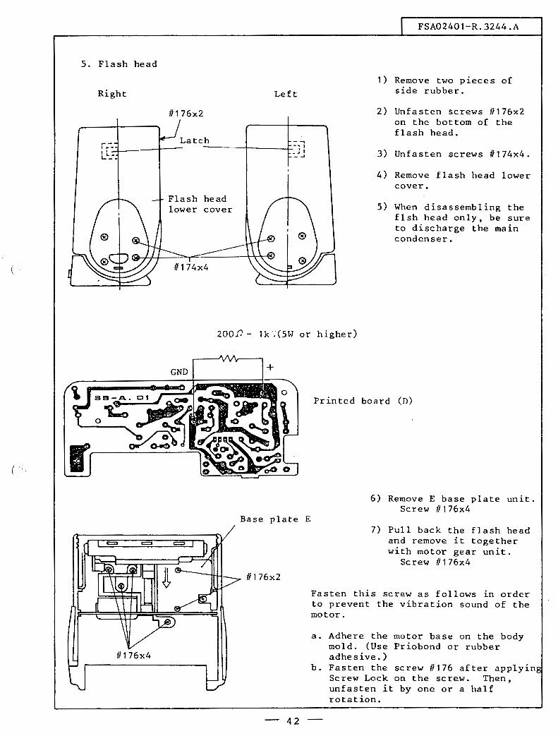
5. Flash head
Right
111 76x2
.- --: r-:.:·1----t--l-'-_-_
11176x4
Left
- ., ----~--t-~~~+,-~ I
• • I - -'
FSA02401-R.3244.A
1) Remove two pieces of side rubber.
2) Unfasten screws #176x2 on the bottom of the flash head.
3) Unfasten screws #174x4.
4) Remove flash head lower cover.
5) When disassembling the flsh head only, be sure to discharge the main condenser.
200.r:' - 1 k ·;(SW or higher)
Base plate E
fl 1 76x2
Printed board (D)
6) Remove E base plate unit. Screw (/176x4
7) Pull back the flash head and remove it together with motor gear unit.
Screw f/ 176x4
Fasten this screw as follows in order to prevent the vibration sound of the motor.
a. Adhere the motor base on the body mold. (Use Priobond or rubber adhesive.)
b. Fasten the screw #176 after applyin Screw Lock on the screw. Then, unfasten it by one or a half rotation.
- 42 -

8180 fl 1 7 5x4 fl 1 80 8) Ma~n condenser cover
Screw fl 180x2 fl 175x4
Note: Soldering of trigger coil
Be careful that the end of wire or pickle of solder does not protrude.
6. Autofocus illuminator panel
-]) \
1) Take off the mounting foot.
2) Take off the autofocus illuminator panel, while pushing two latched portions at its bottom.
-41 -

(
FSA02401-R.3244.A
How to arrange lead wires (brown, gray, black, purple) connected to reflector
x
Turning point of purple wire
=
(B) 30mm
(A) 50mm
x
>
5--lOmm
0
-44
(A) Turn four lead wires by the length of SOmm.
(B) Attach adhesive tape of 12nun width to the lead wires and wind adhesive tape of 6mm width on the wires double or triple.
Pass four wires (brown, gray, black, purple) between two condensers (0.047pF) and fix them together with the condensers using adhesive tape of 6nun width.
Arrange five lead wires (green, yellow, black, purple, white) connected to the flash head on the double-pole connector.
If the reflector moves between the 24nnn and 8Smm setting positions, four lead wires should be inside the range indicated by dotted lines.

I FSA02401-R.3244.A
IX. ADJUSTMENT PROCEDURE
a) Outline There are six adjustment points; five variable resistors (VRt - VR5) and the focus assist illuminator angle. Because adjustment of the vaiable resistors VRl - VR5 is an electrical one, the order of adjustment procedure should be followed exactly.
VRt: Safety circuit voltage (350±3V) VR2: Recycling completion voltage (330±2V) VR3: Flash output in M & MR mode VR4: Flash output in A mode VR5: Gammer in M, MR or A mode (regulated current)
Order of adjustment:
IMPORTANT
VRl -- VR2 -VR5 <VR3 VR4
t. Since a monitor oscillation method is employed, the main condenser may be damaged if a DC regulated voltage of 5.7V as a power supply voltage is applied. Follow Adjustment Procedure b).
2. After finishing the adjustment of VR5, adjust VR3 and VR4. Then, if VR5 is readjusted again, VR3 and VR4 must be readjusted. However, even if VR3 (VR4) is readjusted, it's unnecessary to readjust VR4 (VR3).
3. Variable resistors VR1 - VR5 must be readjusted respectively when the parts listed below are replaced.
VRl: Pinted circuit B, R6, R36, VR1, DS, Qt
VR2: Printed circuit A, Printed circuit B, R7, RB, R9, R37, VR2, U2
VR3: VR3 must be readjusted when the flash head is disassembled (when the body mold B is taken off) disregarding replacement of parts. Printed circuit A, Printed circuit B, U2, D27/28, Q22, C22, C23, VR3, VR5, R44, R45, R46, R47, R48, R49, R50, R78, R53, R54
VR4: Printed circuit A, Printed circuit B, U2, D33 (VR4 must be readjusted when D33 is taken off from the body mo~d E and again mounted.), Q22, C22, C23, VR4, VRS, D27/28, R45, R46, R47, R48, R49, RSO, R78, R53, R54
VR5: Printed circuit A, U2, R53, VR5, R78
-45
(
(

FSA02401-R.3244.A
b) Adjustment Procedure
TP1
TP2
Variable resistors VR1 - VRS can be adjusted after removing autofocus illuminator panel. However, the test point on the printed circuit B, which is used to measure the voltage, is not so close to the hole of the body mold E, and it is difficult to make contact. Therefore, it may be easier to adjust VR1, VR2 and VR5 after removing the body mold E to make the contact surely, because adjustment of VR1, VR2 and VR5 requires measurement of voltage.
Be careful of the high voltage of the main condenser when disassembling.
Use a DC regulated power supply (5.7V, 2A) if not specified.
TP3
GND can be taken on the circumference of the sync connector or the right pin of the external power source terminal.
The state after autofocus illuminator panel is removed. Fig. 1
Base plate B2
- 46

1) VR1 (Safety circuit voltage)
Adjustment of VR1 is to decide the voltage (350V) at which the safety circuit starts operation. As shown in Fig.1, by turning the variable resistor VR1 in a clockwise direction, the voltage decreases. Boost the monitor voltage by turning VR2 fully in a counterclockwise direction, then adjust. As shown in Fig.2, connect the SB-24 with a DC regulated power supply and apply approx. 5.2V as the power source voltage. (current limit: 1A) Connect a digital voltmeter between TP3 and GND shown in Fig.1. Adjust VR3 to start firing the SB-24 when the voltage at this point reaches 350±3V.
FSA02401-R.3244.A
Fig.2
Note: Be careful that the voltage in the main condenser does not exceed 355V in adjustment.
The power automatically turns off unless the ready-light lights up for 60 seconds. In this case, turn off the power SW once, and then turn it on.
2) VR2 (Monitor voltage)
VR2 can be adjusted to maintain the terminal voltage of the main condenser at 330V, and also to decide the voltage for ready-light lighting. Adjust VR2, so that the voltage of TP3 is 330V. (By turning VR2 clockwise, the voltage decreases.) If the main condenser voltage reaches the monitor voltage once, ascillatio~ stops. Oscillation does not start again in 32 seconds at longest. Accordingly, once the oscillation stops at the monitor voltage, it is necessary to fire the flash by pushing the openflash button.
The adjustment of the voltage to light up the ready-light can also be completed by the above adjustment. Set the voltage of the DC regulated power supply at 3.8 - 4.0V and make sure that the readylight lights up at the voltage of 260 - 268V. Guide number inunediately after the ready-light lights up is:
3) VR5 (Gamrner)
GN = 25+5 (ISO 100, rn, 35mrn) at manual full power -2
VR5 is adjusted, so that the level of light output in A, M or MR mode can be set correctly. Connect a voltmeter between TP4 and TP5. Then, adjust VR3, so that the voltmeter reads 18.4mV. (By turning VRS clockwise, the voltage decreases.)
- 47-
(
\
(
(
I FSA02401-R.3244.A
4) VR3 (Flash outpu,t in M & MR mode)
Place the SB-24 two meters away from a flashrneter, and fire it by pushing the open-flash button or by closing the X contact. With the flash mode selector set to M, the light amount 1/16 and the zoom setting 35rnm, adjust VR3, so that the value on the flashmeter should be as follows: (By turning the VR3 clockwise, the light amount increases)
F4 - F4.25 (F4~g· 17EV) GN8 - GN8.5
All the light amount in M mode (1/16 - 1/1) and in MR mode (1/16, 1/8) can be adjusted by the above adjustment at Ml/16 setting. Inspect the flash output at each setting (at least with zoom 28mm & 35mrn setting) in accordance with the specifications.
5) VR4 (Flash output in A mode)
Place the SB-24 two meters away from a standard reflector paper, and fire it by pushing the open-flash button or by closing the X contact. Set the flash mode selector to A, ISO film speed to 100, zoom to 35mm and aperture to FS.6. Measure the flash output using a flashmeter and adjust VR4, so that the following value is shown. (By turning VR4 clockwise, the light amount increases.)
F5. 6;t0. 1 (FS.6~0.0SEV)
Inspect the flash output level at each setting as shown below:
ISO 100 100 100 100 100 100 80 80 F No. 2 2.8 4 5.6 8 11 in set 5.6 5.6
F.No. F2+0.SEV F2.8+0.SEV F4+0.5EV F5 .6+0.5EV F8+0.5EV F11+0.5EV F5 6+0.8EV F5.6:-g:~ measured " -0.2EV
6) Adjustment of angle of FL module unit
The pattern of the autofocus assist illuminator should be inside the focus brackets of the camera. If the shoe cover is replaced, the position of the AF illuminator projection may possibly be shifted. Be careful not catch lead wires when screwing the shoe cover, because the FL module unit may be inclined if the wires are caught by the shoe cover.
Note:· 1. FL module is fixed on the body mold Eby two springs (//161) and three screws (#177). The position of the AF illuminator projection can be adjusted by fastening or unfastening these three screws.
2. If the FL module has a problem, replace the whole FL module unit with new one. Focusing of the FL module is already adjusted and only three screws (#177) should be adjusted.
-4a
FSA02401-R.3244.A
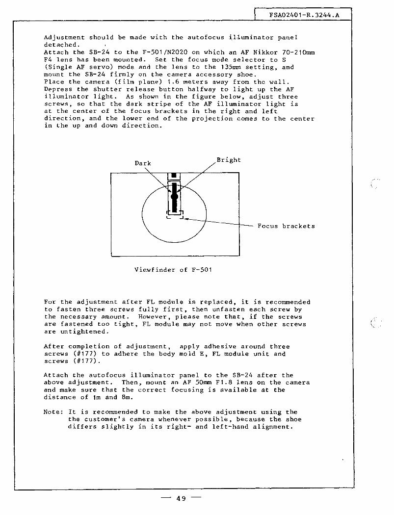
Adjustment should be made with the autofocus il,luminator panel detached. Attach the SB-24 to the F-501/N2020 on which an AF Nikkor 70-210mm F4 lens has been mounted. Set the focus mode selector to S (Single AF servo) mode and the lens to the 135nnn setting, and mount the SB-24 firmly on the camera accessory shoe. Place the camera (film plane) 1.6 meters away from the wall. Depress the shutter release button halfway to light up the AF illuminator light. As shown in the figure below, adjust three screws, so that the dark stripe of the AF illuminator light is at the center of the focus brackets in the right and left direction, and the lower end of the projection comes to the center in the up and down direction.
Dark Bright
Focus brackets
Viewfinder of F-501
For the adjustment after FL module is replaced, it is recommended to fasten three screws fully first, then unfasten each screw by the necessary amount. However, please note that, if the screws are fastened too tight, FL module may not move when other screws are untightened.
After completion of adjustment, apply adhesive around three screws (#177) to adhere the body mold E, FL module unit and screws (11177).
Attach the autofocus illuminator panel to the SB-24 after the above adjustment. Then, mount an AF 50mm F1.8 lens on the camera and make sure that the correct focusing is available at the distance of 1m and 8m.
Note: It is recommended to make the above adjustment using the the customer's camera whenever possible, because the shoe differs slightly in its right- and left-hand alignment.
- 49 -
\,

(
I FSA02401-R.3244.A
X. TROUBLE SHOOTING '
X-1. NORMAL OPERATION
The followings are not troubles.
1-1. LCD * Flash shooting distance indicator goes out when flash head is
rotated or tilts up. * Flash shooting distance indicator blinks when flash head tilts
down. * The display, which should appear when SB-24 is attached on
F-80l/N8008, appears for approx. 0.5sec if batteries are installed at the power SW setting at ON or STBY without a camera.
* When the power SW of SB-24 is switched to STBY from OFF under the condition that SB-24 is attached to F-801/N8008 and the pre-release timer of the camera is off, the display shown for an instant is different from what should be. (ISO 100, F5.6 & 35nun will be displayed.)
* Rear sync mode cannot be used with repeating flash. (In this case, the display of the ntllllber and frequency of repeating flash disappears.)
* A part of LCD is dim. *LCD has unevenness in colour when turned off. * Response speed of display becomes slow or blinking display is
hard to recognize at the low temperature (0°C or lower). (It's characteristics of LCD.)
1-2. Flash firing * When open-flash button is pushed in TTL mode with SB-24
attached to F-801/N8008, the flash may fire at full output or at small amount output.
* Flash may not fire eight times at 1/16 setting or four times at 1/8 setting in repeating flash mode at the low temperature br when fresh batteries are not used. (In the low temperature, it not be restored by warming up only batteries.)
* 1/8 and 1/16 output in repeating flash mode is smaller than that in M mode. (Light amount in repeating flash mode is smaller than that in M mode by 1/3 EV.)
1-3. Power control If ready-light does not light up in 60 sec with power SW set to ON or STBY due to insufficient battery power, the power automatically turns off.
1-4. Others Refer to the page 42 (10-1) in the rpair manual of SB-22. (However, 4th item is not true of SB-24, that is, SB-24 does not turn off if the open-flash button keeps pushed.)
- 50 -
1 FSA02401-R.3244.A
The following inspection is to be made with SB-24 only, if not specified. Battery power should be 6V.
X-2. POWER
2-1
Incorrect current is generated when power source is installed. I ~
Current flows when power is off or in STBY-OFF state. Normally, 20pA or less (actually 5pA) in OFF setting or 100pA or· less (actually 10pA) in· STBY-OFF.
+ 2 11
2-2
LCD fails to light up when power SW is turned to STBY from OFF. I
' Oscillation starts when power SW is turned to STBY from OFF. (Check for oscillation with annneter.)
t NO
LCD lights up when SB-24 is attached to TTL camera (F-801, FE2, etc.) and shutter release button is lightly depresed in SB-24's STBY state.
~ NO
YES -221
YES --222
I Pin 17 of Ul is provided with the voltage 3V YES--223
~ NO
224
2-3
SB-24 turns off (STBY-OFF) in a short time after I power SW is turned to ON from STBY.
NO !Ready-light is lighting. j --~ YES
... I s_T_B_Y_O_F_F_i_n_6_o_s_e_c_ . ....JI YES - 231
I NO
232
Power automatically turns off if ready-light does not light up in 60 sec. (Normal operation)
- 51 -

2-4
Power fails to turn off (STBY-OFF) even if power SW is turned to STBY from ON.
LCD display is normal. switch operation.)
t YES
(changes according to I
I FSA02401-R.3244.A
NO - "3-1 Display"
I Pin 24 of U1 (pin 10 of U2) l. s H (JV). YES -241
~ NO
I Pin 25 of U2 is L (OV). I NO -- 242
~ YES
243
2-5
Power fails to turn off when power SW is switched to OFF I
251
2-6
Power fails to turn on when open-flash button is pushed I in STBY-OFF state.
Flash fires when open-flash button is pushed when power I is on. YES - 271
2-7
t NO
262
Power fails to turn on even if shutter release button is lightly depressed after SB-24 is attached to TTL camera in STBY-OFF state.
Pin 10 of U2 is L (OV) when shutter release button is I YES -271 lightly depressed.
' NO 272
- 52

FSA02401-R.3244.A
X-3. DISPLAY
(Refer to "X-5. DATA COMMUNICATION" as to the display for data communication when SB-24 is attached to F-801/N8008)
3-1
Display fails to be changed by pushing operational buttons or mode selector.
jspecific indicators fail to chang~.
t NO
YES --311
All indicators fail to change. I (Blinking display fails to appear.)
Flash fires when open-flash button is pushed. YES -312
t NO "X-8. FLASH FIRING"
3-2
LCD gleams or display changes with no switch operation. I ---321
3-3
jAll indicators blink. I
' Pin 17 of U1 (VDD) is stably providedwith3V. I YES -331
t NO
332
3-4
LCD shows abnormal data when illuminator button I is pushed. (Illuminator does not light up.) - 341
3-5
!incorrect LCD segment lights up.
~ Voltage at pins 14, 15, 16, 19 is as follows: Pin 19=0V, Pin 14=1V, Pin 15=2V, Pin 16=3V
' YES 352
- 53 -
NO - 351
\
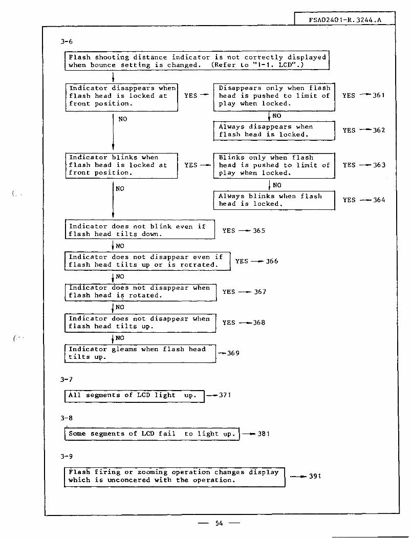
I \-
t·.
FSA02401-R.3244.A
3-6
Flash shooting distance indicator is not correctly displayed when bounce setting is changed. (Refer to "1-1. LCD".)
Indicator disappears when flash head is locked at YES -front position.
Disappears only when flash head is pushed to limit of play when locked.
Always disappears when flash head is locked.
Indicator blinks when flash head is locked at front position.
Blinks only when flash YES - head is pushed to limit of
play when locked.
Always blinks when flash head is locked.
Indicator does not blink even if flash head tilts down. YES -- 365
Indicator does not disappear even if flash head tilts up or is rotrated. YES --366
~NO
Indicator does not disappear when flash head is rotated.
Indicator does not disappear when flash head tilts up.
Indicator gleams when flash head tilts up.
3-7
YES - 367
YES --368
--369
I All segments of LCD light up. 1-371
3-8
f some segments of LCD fail to light up.1-381
3-9
Flash firing or zooming operation changes display which is unconcered with the operation.
- 54 -
--391
YES - 361
YES -362
YES -363
YES --364

I FSA02401-R.3244.A
X-4. OSCILLATION (including monitor circuit)
4-1
Oscillation is not executed (needle of ammeter does not swing if power SW is turned to STBY from OFF) and ready-light does not light up. (In case oscillation is stopped by monitor circuit, it does not start for 32 sec. Therefore, it is necessary to turn off power SW for inspection.)
Oscillation starts if collector andl emitter of Q7 are shortcircuited. NO- 4ll
~YES
IP in 8 of U2 is H (3V). NO - 412
• YES
I Pin 28 of U2 is H (2V or higher)., NO - 413
• YES
!Anode of D34 is H ( 1 v
YES
or higher)· I NO--IBase of Q3 is H (3V).,N0--414
l YES 415 416
4-2
Oscillation is done for an instant (current approx. 0.1A flows) and soon stops. Ready-light lights up. But main condenser is not charged.
4-3
Oscillation does not stop even if power voltage I becomes 3V or lower.
Oscillation is stopped by pushing zoom button before ready-light lights up.
4-4
~ YES
432
NO -431
Oscillation does not stop if zoom button is pushed before ready-light lights up. (Normally, oscillation stops during zoom operation to prevent zoom motor rotation from slowing.)
-421
Oscillation does not stop even if voltage falls below 3V. j YES -- 441
J NO
442
55 -
(

I FSA02401-R.3244.A
4-5
Oscillation stop voltage (330V) is low. (Full flash guide number is small.) -451 Oscillation stop voltage (330V) is high.
4-6
When power SW is turned to ON from OFF after power source (6V, 2A) is connected to SB-24, oscillation does not stop in 20 sec. (If oscillation continues in this condition, excessive voltage is given to main condenser. Therefore, power SW must be turned off innnediately.)
Voltage in main condenser I is over 355V.
YES ----1 Safety circuit fails to operate· I
' NO Pull out connector of lead wire I 0368 from printed circuit unit B
I Oscillation stops. j YES -462
~ NO
463
4-7
i 461
Oscillation stops as soon as ready-light lights up. 1-- 471
4-8
Current of only approx. 0.1A flows while oscillation' 4 is done. Voltage in main condenser does not rise. - 81
- 56 -

FSA02401-R.3244.A
X-5. READY-LIGHT
5-1
Ready-light fails to light up.
Oscillation stop voltage is normal and safety circuit does not operate. (Flash does not fire.) NO - X-4. OSCILLATION
' YES Both ready-light in viewfinder and on SB-24 fails to light up. YES - 51 l
t NO
I Only SB-24 ready-light fails to light up. I YES - 512
~NO
Only viewfinder ready-light fails to light up.
t 513
5-2
Ready-light gradually becomes bright when lighting up. YES ---521
5-3
!Ready-light fails to go out.
Both ready-lights ~n viewfinder and on SB-24 fail to go out.
~ NO
!Only SB-24 ready-light fails to go out. YES -- 532
~ NO
Only viewfinder ready-light fails to go out.
533
5-4
'Recycling time is too long or too short.
'
YES - 531
Voltage to 1 ight up ready-light is approx 265V. YES - 541
t NO
542
- 57 -

(
FSA02401-R.3244.A
5-5
I Ready-light is always blinking. j - 551
X-6. SAFETY CIRCUIT
6-1
Safety circuit fails to operate correctly.
jope-;-ati~ -of ;-onito;- cir~uit -;~t-b;i I stopped to inspect safety circuit. l I Monitor circuit stops operating by 1 I shortcircuiting TP2 and GND. Then, I I voltage in main condenser rises over I L]30~ -- - - - - - - - - -- __ _J
Flash does not fire even if voltage in main condenser rises up to 350V.
f NO
Flash does not fully fire, but repeats firing of small light amount.
t 612
6-2
Flash automatically fires after power SW is turned to STBY from OFF. (Monitor circuit is faulty and safety circuit works.)
YES - 611
Voltage in main condenser is 350V when flash fires. NO - 621
t YES
Oscillation is stopped by pushing zoom button before ready-light lights up.
6-3
~ YES
623
NO - 622
Flash automatically fires when power Sw is turned to STBY from OFF using SD-7 as an external power source.
631
58 -

I FSA02401-R.3244.A
X-7. MODE SELECTOR
7-1
Incorrect flash mode is displayed on LCD. l--x-4. DISPLAY
7-2
Flash mode indicator shows correct flash mode but flash is not controlled in that mode. (for ex. TTL control is made in A mode, or warning is given in M mode before shooting.)
r-----------------1 Make sure of flash mode by lcovering sensor or camera ;
l:_n~ ch~c~in~ th:_ :_igh:._ ~~~t .:J
TTL flash control l.S done in any flash mode.I YES -721
~ NO
I TTL flash control is done in A mode. YES - 722
J NO
TTL flash control l.S done in A or repeating flash mode. I i YES t NO
723 724
Pln"No. of U2 43 44
TTL L L
A L H
M or Repeating H L
- 59 -

(
I FSAC·2401-R.3244.A
X-8. FLASH FIRING
8-1
jFlash fails to fire .
• Flash cannot be fired by pushing NO open-flash button nor shutter release button.
Flash fails t<:' fire only IYES-811 when shutter is released
'NO • YES
Ready-light blinks for 3 sec when shutter release button
Flash fails to fire only when open-flash button is pushed.
~ or open-flash button is N0-813 pushed in A or TTL mode.
t YES 812
I Main condenser is charged up to 330V. NO - X-4. OSCILLATION
' YES I Spark in flash tube can be seen· l NO - 814
t YES
815
8-2
Flash does not fire while oscillation is done. (Fires after after oscillation stops.) Flash may sometimes fire after - 821 full flash warning is given in A or TTL mode.
8-3
Flash fires only once in repeating flash mode. j
+ Flash fires repeatedly when open-flash button is pushed, I NO _
831 but fires once when shutter release button is depressed.
t YES
If settings on camera or SB-24 are incorrect, flash fires only once. a) Shutter speed in set is too fast for repeating flash. b) Flash sync mode selector is set to REAR.
8-4
If frequency and number of repeating flashare set to 10Hz and 8 respectively, flash fails to fire eight times even with fresh batteries.
- 60 -
-- 841

I FSA02401-R.3244.A
8-5
Rear sync flash cannot operate normally (with F-801).1
l Display by ~ata connnunication I NO_ X-lS. DATA COMMUNICATION with F-801 1s normal.
8-6
' YES 851
!Flash automatically fire~.,
Flash automatically fires after power SW is turned I to STBY from OFF. YES - Refer to 6-2.
Flash fires when zoom setting is changed. YES --861
~NO
Flash fires when shutter release button is lightly depressed to light up AF assist YES - 862 illuminator with AF camera.
~NO Flash fires when sync terminal or foot contact is touched with your hand if sync cord is connected YES --863 or SB-24 is attached on camera. (This may occur with normal SB-24, but if it occurs NO ---864 frequently, it must be repaired.)
- 61 -

(
FSA02401-R.3244.A
X-9. FLASH SYNC CONTROL (The follo~ing checking is to be made assuming that the flash mode can be correctly switched.)
9-1
Flash fires fully when ·settings do not permit that.
lFlash fires in any flash mode., YES --
J NO
Flash fires fully only in TTL mode.
Warning is not given after shooting in A or TTL mode when setting do not. permit full flash.
YES - 913 NO ! NO 911
Flash always fires fully in any flash mode (A, M or repeating flash) disregarding F No. and light amount in set.
NO
i YES
912
YES --914
Flash fires fully only in A mode disregarding F No. in set. YES ---915
NO
Flash fires fully in M and repeating flash modes disregarding light amount in set.
NO
YES -916
Flash sometimes fires fully if mode selector is switched. ---917
9-2
I Flash output is insufficient ·I +
Flash output is insufficient in any flash mode. YES -- 921
t NO
Flash output is insufficient only in TTL mode. YES -922
~ NO
Flash output is insufficient in A, Mand repeating mode. YES ~923
! NO
Flash output is insufficient only in A mode. YES -- 924
~ NO
.Flash output is insufficient in M and repeating flash mode. --925
- 62 -

I FSA02401-R.3244.A
9-3
Flash may sometimes fire at incorrect output in A mode if F No. and ISO film speed is switched. Flash may sometimes fire at incorrect output in M mode if light amount or zoom setting is changed.
9-4
--931
Light amount in M mode cannot be changed by adjusting VR. I -- 941
9-5
Flash output is unstable for every shot in A, I--951 M and repeating mode.
~~~~~~~~---==-~~~~~~~~~~~~~~~~~~
9-6
Over-exposure happens when subject is close.I -961
9-7
Gannner adjustment is impossible with VRS.1- 971
X-10. WARNING
10-1
!Blinking of ready-lights fails to stop. I- 1011
10-2
Blinking frequency for ready-light warning is incorrect. j ---1021
10-3
Duration for warning (after shooting) is incorrect. I --- 1031
10-4
Warning is given before shooting in A, M, or repeating flash mode. __ 1041 Warning is given after shooting in M or repeating flash mode.
- 63 -

I FSA02401-R.3244.A
10-5
Warning is given before shooting in TTL mode even if settings are correct.
Voltage at pin 25 of U2 is 3V or lower when I shutter release button is lightly depressed. YES ---lOSl
~ NO
!voltage at pin 23 of U2 is 3V or lower. YES ---1052
• NO
1053
10-6
Warning before shooting fails to appear. j
• I Flash mode is not switched to TTL. I YES -- Refer to 7-2.
t NO
I TTL incable warning fails to appear. jYES --1061
i NO
Over usable film speed warning fails to appear. I YES - 1062
10-7
Warning fails to appear even if flash fires fully I in A or TTL mode.
jFlash mode is not switched to A or TTL. JYES-- Refer to 7-2.
X-11. ZOOM
11-1
' NO 1071
Zooming motor fails to operate though zoom setting display changes. (Finally " "will be displayed.)
11-2
Zooming motor continues rotating and clutch is disengaged. Then, "--" is displayed, reflector moves to 24mm position (sometimes does not) and motor stops.
- 64 -
-1111
-1121

FSA02401-R.3244.A
11-3
Reflector moves back and forth repeatedly and does not stop. Then, "--" is displayed, reflector moves to 24nnn position -1131 (sometimes does not) and motor stops.
X-12. AF assist illuminator (The following checking is to be made assuming that warning before shooting is correctly operating.)
12-1
\AF assist illuminator fails to light up.
t One LED of AF assist illuminator fails to light up.
~ NO Set power voltage to 3V, current limit to O.SA and shortcircuit pin 22 and 21 of U2. Then, AF assist illuminator lights up.
l NO Voltage at base of Q13 is 1.SV or higher when pin 22 and 21 is shortcircuited.
12-2
~ YES
1215 t NO
1214
YES Each LED can light up by itself. (See below for inspection of LED)
YES-1213
j YES
1211
r---------------, Checking AF assist illuminator: 1 Pull off connector of AF assist I
illuminator from base plate and I connect it to the circuit shown I below. Then, confirm that LED I lights up. White I
I W I
I I I I
L Yellow 1 _______________ _)
IAF assist illuminator fails to go out.
AF assist illuminator is always lighting if power SW is ON. YES --1221
i NO AF assist illuminator is always lighting while shutter release button is lightly depressed.
t 1222
- 65 -

( .
(
FSA02401-R.3244.A
12-3
AF assist illuminator lights up for a moment when CSP contact is open and CRY contact is grounded. This may occur SB-24 is attached to camera which has only X contact on accessory shoe.
-1231
12-4
Position of AF illuminator projection is incorrect.
--- Refer to "Adjustment of angle of FL module".
X-13. LCD ILLUMINATOR
13-1
'LCD illuminator fails to light up. 1--1311
13-2
LCD illuminator is bright than normal one and becomes darker while zooming or oscillation is executed. (Even normal illuminator may become darker while zooming or oscillation is executed.)
13-3
I LCD illuminator is dark. - 1331
X-14. OFFENSIVE ODOR
14-1
I offensive odor is given.
t I R22 is burnt. j YES --1411
NO
!safety valve of main condenser is open.I
~ 1412
66 -
-- 1321

I FSA02401-R.3244.A
X-15. DATA COMMUNICATION
The following checking is to be made assuming that SB-24 operates by itself or in combination with F-501. SB-24 is to be attached to F-801. The listed bwlow are foreseen troubles. If they are not applicable to actual troubles, check for the wiring (short circuit and poor soldering) used for data communication.
Lines used for data communication are as follows:
Between foot contact and U2: (Check it using F-501. If viewfinder ready-light, TTL flash control and warning is normal, connection is correct.) Foot contact CSP~C34-L3-R62-C42-Pin 25 of U2, Wire #380(brown) Foot contact CRY-C35-L5-R60-Pin 24 of U2, Wire #380(green) Foot contact CSTP-C33-L2-R63-Pin 23 of U2, Wire #380(gray) #377{yellow~
15-1
Between U2 and Ul: I Pin No. of U2: I 2 I 3 I 4 I 5 I 10 I 11l12T13114 I Pin No. of U1: I 40 I 39 I 38 I 37 r 24 I 23 I 22 I 21 I 20
When pre-release ON: 1) Display "F" blinks. 2) Display of !SO, F and ZOOM does not change even
if settings are changed. When pre-release OFF: 1) ISO and flash shooting distance indiactors go out. 2) Display "F" blinks and F No. does not go out.
15-2
1) SB-24 shows the display which should appear when SB-24 is not attached to camera.
2) Displays for ISO, F and ZOOM does not change even if settings are changed.
15-3
Pre-release ON: Normal
-1511
--1521
Pre-release OFF: SB-24 shows the display which should appear --1531 when SB-24 is not attached to camera.
- 67 -

J FSA02401-R.3244.A
CAUSES OF TROUBLES
"Failure of Part A" includes poor soldering or short circuit of the part A. If the cause of trouble is mainly considered short circuit or open circuit, the part number is marked with (S) or (0) , respectively. "Poor connection of lead wire" or "Poor connection of FPC" includes poor soldering or poor contact of connector. Vee and GND of IC is to be connected surely.
CAUSES OF TROUBLES
Short circuit or some part is faulty in the circuit. Power source line is divided into six listed below. Search the circuit for abnormal current referring to circuit diagram.
211 1. U1 line (D1) 2. U2 line (D2) 3. Oscillation 1 ine 4. FL module line 5. LCD illuminator line 6. Motor driving line (Leak current flows at QS & Q6 if R3 1S open, and oscillation is executed even if power SW is off when pins 8 and 9 of U2 are shortcircuited.)
221 Failure of LCD, Poor contact (fal 1 down) of LCD rubber connector; Failure of Ul or R76 (0)
222 Failure of C39 (0) or R65 (0)
Failure of U1 , Poor contact of power SW; Failure of 32kHz oscillation circuit (CLK1, C28, C29, R71, R72), lMHz oscillation circuit (CLK2, C30, C31, R70) or U4; Poor connection of FPC (i);
223 Poor connection of FPC (p); Short circuit in FPC (o-p, p-q); Failure of R79; Short circuit in Ul (23-24, 24-25, 25-26, 26-27, 27-28, 28-29, 29-30' 30-31 , 31-32); Short circuit in U2 (9-10, 10-11) ; Poor soldering of pins 25, 26, 27, 29, 30, 31 of Ul
Batteries are reversely installed.; Poor contact of battery 224 contact (too large positive contact or dust on contact); Poor
connection of lead wire 11376; Failure of Dl (0), R64 (0) or U3; Poor connection of FPC (i)
231 Poor soldering of pin 58 of U2; Failure of Ul
232 Poor contact of power SW; Poor soldering of pin 53 of Ul; Failure of Ul; Short circuit in U1 (53-52' 53-54)
241 Poor contact of power SW; Poor soldering of pin 53 of Ul; Failure of U1; Short circuit in U1 (53-52, 53-54)
Cuurent is flowing into CSP contact. Short circuit between lead 242 wire tf 380 (brown: CSP line) and other 1 ine s; Short circuit in U2
(24-25' 25-26); Failure of U2
243 Failure of R70 (0), R65 (S) ' C39 (S) , U2 or U1
251 Poor contact of power SW; Poor soldering of pin 53 of u 1; Failure of Ul
. 261 Poor soldering of pin 10 of U2; Failure of U2
262 Ref er to "X-8. FLASH FIRING".
- 68 -

271
272
311
312
321
331
332
341
351
352
361
362
363
364
365
366
367
368
369
I F'SA02401-R.3244.A
Poor soldering .of pin 10 of U2; Failure of U2
Failure of C34(S), C42 (S) , L3 (0), R62(0) or U2; Poor connection or short circuit of lead wire #380 (brown)
State of switches are read by key matrix. Refer to circuit diagram and look for switch which is not read. Parts and U1 terminals concerned are as follows: R31, R32, R33, R34, R35, C15, C16, C17, C18, C19, D17/18, Dl 9 /20, D21/22, D23/24, D25/26, D35/36, D37/38 Ul switch matrix Input pin 60, 61 , 62, 63, 64, Output pin 52, 53, 54, 55, 56 For slide SW, inspect poor contact of switch brush.
Short circuit between pin 27 of U1 (pin 9 of U2) and other lands; Poor soldering of pin 27 of Ul or pin 9 of U2; Failure of Ut or U2
Failure of R31(0), R32 (0), R33(0), R34(0), R35(0), C15(0), Ct6(0), C17(0) Ct8(0) or C19(0); Poor soldering of pin 60, 61 62, 63 or 64 of Ul; Failure of Ul
Failure of U4, R31(0), R32(0), R33(0), R34(0), R35(0), C15(0), C16(0), C17(0), C18(0) or C19(0); Poor soldering pin 60, 61, 62, 6 3 or 64 of U 1 ; Failure of Ul
Failure of Dl(S), C36 (0) , R64(0), U3 or C37 I
Poor connection of lead wire 11378; Failure of illuminator; Failure or poor soldering of T3
Failure of R73, R74, R75 or U1
Short circuit in Ul (1-13, 65-80); Failure of Ul
Play of bounce lock is too large. (If material of bounce lock part is deformed, replace it.)
Short circuit between lead wires 11371 (white and black) or between 11372 (black) and 11373 (white)
Play of bounce lock is too large. (If material of bounce lock part is deformed, replace it.)
Short circuit between lead wires 11371 (yellow and black)
Poor connection of lead wires 11371 (black and yellow); Failure of D19(0); Poor contact of bounce SW (Down) (11333' //186)
Poor connection of lead wires 1/371 (black and white); Failure of D21(0)
Poor contact of bounce SW (Right/Left) (f/334' fl 186) ; Poor connection of lead wires #372 (black) and 11373 (white)
Poor contact of bounce SW (Up) (fl333, 11186)
Poor contact of bounce SW (Up) (t/333' 1/186); Remove switch grease completely.
- 69 -
(
I,

I FSA02401-R.3244.A
371 Short circuit between pins of U1 and some line of 3V or higher.; Short circuit in FPC (i-j); Failure of U3 or U1
Poor soldering of pin 1-13, 65-72 or 74-80 of U1; Dislocation of 381 LCD rubber connector; Poor contact of LCD rubber connector (Wipe
out LCD, rubber connector and base plate with alcohol.); Failure of LCD or U1
391 Failure of C15(0), C16(0), C17(0), C18(0), C19(0), C20(0), C21(0) or C47(0)
411 Failure of Q5, Q6, C2, R3, D3, T1, R
412 Poor soldering of pin 34 of U1 or pin 8 of U2; Short circuit in U1 (33-34, 34-35) or in U2 (7-8); Failure of U1 or u2
Poor connection of FPC (k); Short circuit in U2 (14-15, 27-28, 413 28-29, 30-31, 41-42, 42-43) or in FPC (b-c, c-d);
414
Failure of C41(S) or U2
Poor soldering of pin 28 of U2; Failure of Rt (0) or Q3
Poor connection of FPC (c);
415 Failure of D34, R2(S), Q7
416 Failure of U1
421
431
432
441
442
451
Failure of D6(0); Poor connection of lead wire #370
Failure of Q7, R2(0), D3(0), D34 (S)
Failure of U2
Failure of Q7, R2(0), D3(0), D34(S)
Failure of QJ; Poor connection of FPC ( s) ; Poor soldering of pin J3 of U1; Failure of U1
Incorrect adjustment of VR2; Failure of VR2, R7, RB, R9, R37, C6, C26, C27 or U2; Leak in FPC (a, b)
Failure of both monitor circuit and safety circuit (Safety valve of main condenser may be open. Inspect bottom of main condenser.
461 If there is a hole on rubber portion, replace main condenser. Refer to 6-2 and 6-1, as to monitor circuit and safety circuit, respectively.)
462 Leak or short circuit of high voltage line on printed circuit D or main condenser
Failure of oscillation circuit (Q5, Q6, C2, RJ, Q7, DJ, RS, T1, CJ 463 or D4); Leak or short circuit of high voltage line on printed
circuit B
471 Failure of RJ7(S); Short circuit in FPC (a-b) or in U2 (29-30)
481 Failure of D4(0) or T1
511 Failure of VR2 (b) or U2; Poor connection of FPC (b); Poor soldering of pin 29 of U2
- 70 -

I FSA02401-R.3244.A
512 Failure of D29, RS 1 (0) , R52(S), U2 or U1; Poor soldering of pin 41 of U2
513 Failure of R60(0), L3 (0) , C35(S) or U2; Poor connection or short circuit of lead wire 11380 (green)
521 Failure of C26(0)
531 Short circuit in U2 (28-29' 30-31) or in FPC (b-c) ; Failure of U2
532 Short circuit in U2 (41-42); Failure of U2
533 Failure of U2; Short circuit between lead wire 11380 (CRY line, green) and other lines
541 Poor connect1on of lead wire fl 376; Failure of C1(0); Failure of oscillation circuit (Q5, Q6, C2, R3, Q7, D3(S), RS, T 1, C3 or D4)
542 Incorrect adjustment of VR2; Failure of VR2, R6, R7, R9, R37, C26, C27 or U2; Leak in FPC (a' b)
551 Short circuit in U2 (42-43); Failure of U2
611 Incorrect adjustment of VR 1; Failure of VR1, R6, R36, R4, D5, C4(S), CS(S), Q1 or Q2; Poor connection of lead wire 11368; Refer to "X-8. FLASH FIRING".
612 Failure of d8(0) or D12(0)
621 Incorrect adjustment of VR 1; Failure of VR1, R6, R36, R4, DS, C4(S), CS (S) or Q1
622 Failure of oscillation (control) circuit (Failure of Q7, R2(0), D3(0), D34 (S))
Failure of monitor circuit (Incorrect adjustment of VR2; Failure of 623 VR2, R6 (0), R7(S), R9 ( S) , R3 7 (S) , C26 (S), C27 (S) or U2; Leak in FPC
(a' b); Poor connection of FPC (a))
6 31 Failure of C4 (0)
721 Short circuit in U2 (43-44) or in U1 (43-42); Poor soldering of pin 43 and 44 of U2 (pin 43 and 42 of U1); Failure of U2 or Ut
722 Poor soldering of pin 44 of U2 (pin 42 of Ul); Failure of U2 or U1
723 Poor soldering of pin 43 of U2 (pin 43 of u1); Failure of U2 or U1
724 Failure of U2 or U1
811 Poor connection of lead wire #380 (X contact, GND line) (red, black) Failure of L4; Poor soldering of foot contact
812 Poor contact of open-flash button (Bend of contact, poor soldering or peeling of printed circuit pattern
- 71 -

I FSA02401-R.3244.A
1) Short circuit of X contact line (X contact fails to open.); Short circuit of lead wire 11380 (X line) (red); Short circuit
in U2 (25:...26' 26-27); Failure of D31(S), Q4 or Q21
813 2) X contact line is open. (X contact signal fails to reach U2.); Failure of D30(0), C32(S), C43(0), C44 (S), R41 (0) or R61(0); Poor soldering of pin 26 of U2
3) Failure of U2
Short circuit in U2 ( 1 7-18, 19-20); Poor connection of FPC (rn)
814 Short circuit in FPC (m-n); Poor conneciton of lead wire 11366, 11367 or /1368; Failure of R66 (0), D8(S), CR 1 (S) , SCRl, Rll(O), C9 T2 or C10(S); Trigger is discharged at other part than flash tube.
815 Poor connection of lead wire /)366; Failure of Xe tube, SCR2, SCR3, R15(S), R16(S), R20(0), C12(0), C13(0), R14(0) or R18(S)
821 Safety circuit is always ON.; Failure of R6 (S), R36(0), VR 1, D5 (S) , Q1 or Q2
Failure of Q4. Q21 or Q24; Poor soldering of pin 6, 9 of U2 or pin 831 27, 36 of U1; Short circuit in U1 (27-28, 35-36) or in U2 (6-7,
9-10); Failure of U2 or U1
841 Incorrect setting of light amount (Refer to Adjustment.); Failure of R20 (If R20=1 kn_ , replace it wkith 560{} . )
Failure of Q4, Q21 , Q24; Poor soldering of pin 7,. 9 of U2 or pin 851 27, 35 of U1; Short circuit in U1 (2 7-28, 35-36); Failure of U2
or Ul
861 Failure of CR1(0), C4(0), C5(0), C20(0), C21(0), C32(0), C44(0), C47 (0) or U2
862 Short circuit in FPC (1-m)
863 Failure of C44(0), C32(0) or Q24
864 Failure of CR1 (0), C4(0), C5(0), C44 (O), C32(0), Q4. Q24 or U2
Poor soldering of pin 19 of U2; Poor connection of lead wire 11368 911 (white); Failure of R23 (O); Failure of commutating circuit,
SCR1, R 18, R21(S), R22, R23(0), D12(S), D10 (0), C12 or C14(S)
Poor connection of lead wire 11368 (purple); Failure of Cl, R22, 912 Q19, R67, C40; Poor soldering of pin 20 of U2; Short cirucuit in
U2 (20-21); Failure of U2
913 Poor connection of lead wire 11380 (gray); Failure of R63(0); Poor soldering of pin 23 of U2; Failure of U2
. soldering pin 37 U2; Short circuit in U2 (37-38, 36-37); Poor of of
914 Poor contact of mode selector SW; Failure of U2, Ul D27/28, C22 (S), C24(S), C25(S), VR5, R49, R50, R53 or R78(0); Short circuit in FPC (h-i, d-e, e-f); Poor connection of FPC (e' f)
915 Poor soldering of pin 3 of U2; Poor connection of lead wire /1379; Failure of D33(0), D27(S), D28(0) or VR4; Poor connection of FPC (g) Poor contact of mosw selector• SW
- 72 -

I FSA02401-R.3244.A
Poor soldering of pin 32 of U2; Short circuit in U2 (31-32); 916 Poor connection of lead wire f/374; Poor connection of FPC (h);
Failure of R32(0), D27(0), D28(S), VR3(0) or R44(0); Poor contact mode selector SW
917 Poor contact of mode selector SW
921 Short circuit in U2 (18-19); Failure of C14(0), D12(0), C40(0), R 10 (S), R21 (0), R6 7 (S) , Q19 or U2; Short circuit in FPC (k-1)
922 Failure of C33(S); Short circuit of lead wire f/377 (yellow) or #380 (gray) with other 1 ines; Short circuit in U2 (23-24)
923 Poor soldering of pin 34 or 36 of U2; Failure of R49(0), R54(0) C22(0) or U2
924 Incorrect adjustment of VR4; Failure of VR4 or D33(S); Short circuit of lead wire 11379; Short circuit in FPC (f-g)
925 Incorrect adjustment of VR3; Failure of VR3, D32 (S) or R44(S); Short circuit of lead wire 11374
931 Failure of C22(0), C23, Q22, Q23, R45, R46, R47, R48 or u 1; Poor soldering of pin 44, 45, 46, 47, 48 or 51 of U1
941 Mounting position of D32 or SPD filter (//135) is incorrect.
951 Failure of C24(0), C25(0), C40(0), R67(S) or Q19; Poor connection of lead wire 11374 shield wire
Failure of D9(0), D10, SCR3, R13(0) or R14(S); SB-24 is provided with commutating flash eliminating circuit and
961 flash firing after commutating is not found in the normal condition as shown in Fig. 1. However, if this circuit has a trouble, additional flash is output like other speed light as shown in Fig.2
Poor connection of FPC (e • f' g, h); Short circuit in FPC (d-e, 971 e-f, f-g, h-i); Poor contact of mode selector; Poor soldering
of pin 38, 35 of U2; Failure of R53, R50, R44, R78, C25(S), VR5, VR3, VR4, U2 or Ul
1011 Short circuit in U2 (42-43); Failure of U2
1021 Failure of C41 or U2
1031 Failure of C41 or U2
1041 Refer to X-7. "MODE SELECTOR".
Poor connection of lead wire 11380 OC SP 1 ine (brown); Short circuit 1051 between lead wire #380 (brown) and other line; Poor solering of
CSP line or pin 25 of U2; Failure of C34(S), C42(S), L3(0) or R62(0)
Light amount Light amount
+ +
r -- t
/l -- t
Fig. 1 Fi2. 2
- 73 -

I FSA02401-R.3244.A
1052 Short circuit between lead wire 11380 (gray) or 11377 (yellow) CSTP line with other l,ine; Failure of C33(S) or U2
1053 Failure of U2
1061 Short circuit between lead wire 11380 (brown) CSP line and other line; Short circuit in U2 (24-25, 25-26); Failure of U2;
1062 Poor connection of lead wire 11380 (gray) CSTP line; Poor soldering of CSTP line; Failure of L2(0) or R63 (0)
1071 Failure of U2
Failure of motor (11269); Poor connection of motor lead wire or lead 1111 wire 1136 9; Poor connection of FPC ( j) ; Poor soldering of pin 49, 50
of Ul; Failure of U5; Sticking of motor gear
1) If zooming head does not move to specified position: Arrangement bend of lead wires (1136 7, 11368) is not correct. (This 15 liable to occur in low temperature.)
1121 2) If zooming head position cannot be detected even though it moves to specified position: Poor connection of lead wire 11369; Poor contact of zooming head detection brush 11155; Poor soldering of pin 52 of U2; Failure of D35/36 or D37/38
Since zooming head position could not be detected, zooming head passes through specified position and returns in reverse direction detecting
11 31 next zooming position. And this procedure is repeated.: Poor connection of lead wire II 369; Poor contact of zooming head detection brush 11155; Poor soldering of pin 52 of U2; Failure of D35/36 or D37/38
1211 Failure of Q14, Q15, R25(0) or R26 (0); Poor connection of AF module lead wire
1212 Failure of AF module; Poor connection of AF module lead wire
1213 Poor connection of FPC (d); Poor soldering of pin 27 of U2; Failure of U2
( 1214 Poor connection of FPC (1); Failure of R24, R25, R27, R28, Q13, Q14
or Q15; Poor connection of AF module lead wire
1215 Short circuit between lead wire 1137 5 (white) c line and other line; Failure of Q10, Ql 1 or C46(S)
1221 Short circuit in U2 (21-22) or in FPC (k-1); Failure of U2 or U1
1222 Short circuit between CRY line and other line; Short circuit of lead wire 11380 (green) CRY line; Failure of C35(S) or U2
1231 Failure of Q11 or C46(0); Poor connection of FPC (q)
Poor connection of lead wire II 3 7 8; Failure of LCD illuminator, 1311 Q16' Q17, Ql 8' R29(0), R30(0) or Ul; Poor connection of FPC (r);
Short circuit in FPC (q-r, r-s)
1321 Failure of regulated current circuit, Q18 or R30(S)
1331 Failure of LCD illuminator or T3
- 74 -
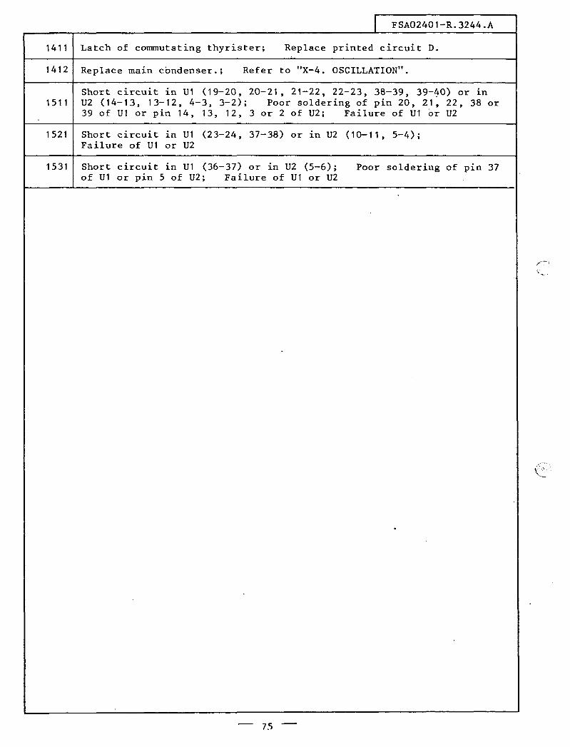
I FSA02401-R.3244.A
1411 Latch of commutating thyrister; Replace printed circuit D.
1412 Replace main condenser.; Refer to "X-4. OSCILLATION".
Short circuit in U1 (19-20, 20-21, 21-22, 22-23, 38-39, 39-~0) or in 1511 U2 (14-13, 13-12, 4-3, 3-2); Poor soldering of pin 20, 21, 22, 38 or
39 of U1 or pin 14, 13, 12, 3 or 2 of U2; Failure of U1 or U2
1521 Short circuit in U1 (23-24, 37-38) or in U2 (10-11, 5-4); Failure of U1 or U2
1531 Short circuit in U1 (36-37) or in U2 (5-6); of U1 or pin 5 of U2; Failure of U1 or U2
- 7.5 -
Poor soldering of pin 37