spf05f0a - seoul semiconductor
TRANSCRIPT
Product Brief
Description
Key Applications
Features and Benefits
www.seoulsemicon.com
Product Data Sheet
Rev1.2, Sep. 2019
SPF05F0A
• The Z-Power series is designed for high
flux output applications with high current
operation capability.
• It incorporates state of the art SMD
design and low thermal resistant
material.
• The Z Power LED is ideal light sources
for directional lighting applications such
as Spot Lights, various outdoor
applications and high performance
torches .• Architectural Lighting
• Stage Lighting
• Exterior Lighting
S1C0-4758150000-00000000-00001
RoHS
• Super high Flux output and high Luminance
• Designed for high current operation
• SMT solderable
• Lead Free product
• RoHS compliant
Superior Efficacy & Lumen output with Small Form Factor

www.seoulsemicon.com2
Product Data Sheet
Rev1.2, Sep. 2019
Table of Contents
Index
• Product Brief 1
• Table of Contents 2
• Performance Characteristics 3
• Characteristics Graph 4
• Color Bin Structure 9
• Mechanical Dimensions 10
• Reflow Soldering Characteristics 12
• Emitter Tape & Reel Packaging 13
• Packaging Information 15
• Product Nomenclature 16
• Handling of Silicone Resin for LEDs 17
• Precaution For Use 18
• Company Information 21
www.seoulsemicon.com3
Product Data Sheet
Rev1.2, Sep. 2019
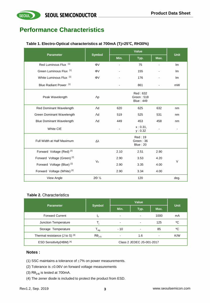
Performance Characteristics
Table 1. Electro-Optical characteristics at 700mA (Tj=25℃, RH30%)
Notes :
(1) SSC maintains a tolerance of 7% on power measurements.
(2) Tolerance is 0.06V on forward voltage measurements
(3) RθJ-S is tested at 700mA.
(4) The zener diode is included to protect the product from ESD.
Parameter SymbolValue
UnitMin. Typ. Max.
Forward Current IF - - 1000 mA
Junction Temperature Tj - - 125 ºC
Storage Temperature Tstg - 10 - 85 ºC
Thermal resistance (J to S) [3] RθJ-S - 1.6 - K/W
ESD Sensitivity(HBM) [4] Class 2 JEDEC JS-001-2017
Table 2. Characteristics
Parameter SymbolValue
UnitMin. Typ. Max.
Red Luminous Flux [1] ФV - 75 - lm
Green Luminous Flux [1] ФV - 155 - lm
White Luminous Flux [1] ФV - 176 - lm
Blue Radiant Power [1] - 861 - mW
Peak Wavelength Λp
Red : 632
Green : 518
Blue : 449
Red Dominant Wavelength Λd 620 625 632 nm
Green Dominant Wavelength Λd 519 525 531 nm
Blue Dominant Wavelength Λd 449 453 458 nm
White CIE -x : 0.31,
y : 0.32- -
Full Width at Half Maximum Δλ
Red : 19
Green : 36
Blue : 20
Forward Voltage (Red) [2]
VF
2.10 2.51 2.90
VForward Voltage (Green) [2] 2.90 3.53 4.20
Forward Voltage (Blue) [2] 2.90 3.35 4.00
Forward Voltage (White) [2] 2.90 3.34 4.00
View Angle 2Θ ½ 120 deg.
www.seoulsemicon.com4
Product Data Sheet
Rev1.2, Sep. 2019
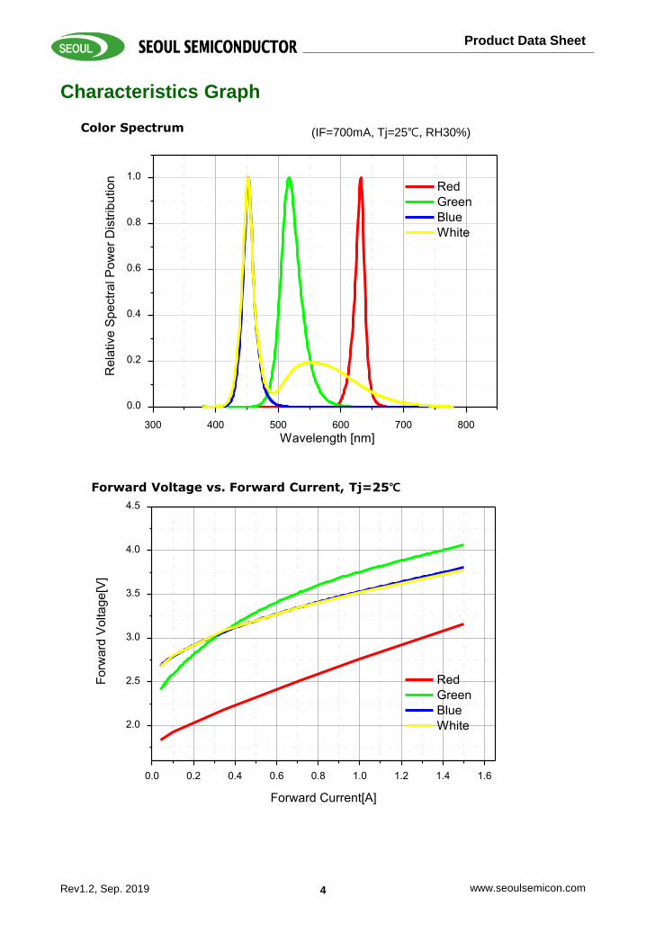
Characteristics Graph
Color Spectrum
Forward Voltage vs. Forward Current, Tj=25℃
0.0 0.2 0.4 0.6 0.8 1.0 1.2 1.4 1.6
2.0
2.5
3.0
3.5
4.0
4.5
Red
Green
Blue
White
Fo
rwa
rd V
olta
ge
[V]
Forward Current[A]
(IF=700mA, Tj=25℃, RH30%)
300 400 500 600 700 8000.0
0.2
0.4
0.6
0.8
1.0 Red
Green
Blue
White
Re
lative
Sp
ectr
al P
ow
er
Dis
trib
utio
n
Wavelength [nm]300 400 500 600 700 800
0.0
0.2
0.4
0.6
0.8
1.0 Red
Green
Blue
White
R
ela
tive
Sp
ectr
al P
ow
er
Dis
trib
utio
n
Wavelength [nm]
0.0 0.5 1.0 1.5 2.0 2.5 3.0
2.0
2.5
3.0
3.5
4.0
4.5
5.0
Red
Green
Blue
White
Fo
rwa
rd V
olta
ge
[V]
Forward Current[A]

www.seoulsemicon.com5
Product Data Sheet
Rev1.2, Sep. 2019
Characteristics Graph
Forward Current vs. Normalized Relative Luminous Flux, Tj=25℃
Forward Current vs Dominant Wavelength, Tj=25℃
0.00 0.35 0.70 1.05
0
100
200
300
400
500
600
700
Red
Green
Blue
White
Do
min
an
t W
ave
len
gth
[n
m]
Forward Current [A]
0.00 0.35 0.70 1.05
0.0
0.5
1.0
1.5
Red
Green
Blue
White
Re
lative
Ou
tpu
t [x
10
0%
]
Forward Current [A]
0.00 0.35 0.70 1.05 1.40
0
100
200
300
400
500
600
700
Red
Green
Blue
White
Do
min
an
t W
ave
len
gth
[n
m]
Forward Current [A]
0.00 0.35 0.70 1.05 1.40
0.0
0.5
1.0
1.5
2.0
Red
Green
Blue
White
Re
lative
Ou
tpu
t[%
]
Forward Current [A]
0.00 0.35 0.70 1.05 1.40
0.0
0.5
1.0
1.5
2.0
Red
Green
Blue
White
Re
lative
Ou
tpu
t [x
10
0%
]
Forward Current [A]
www.seoulsemicon.com6
Product Data Sheet
Rev1.2, Sep. 2019
Characteristics Graph
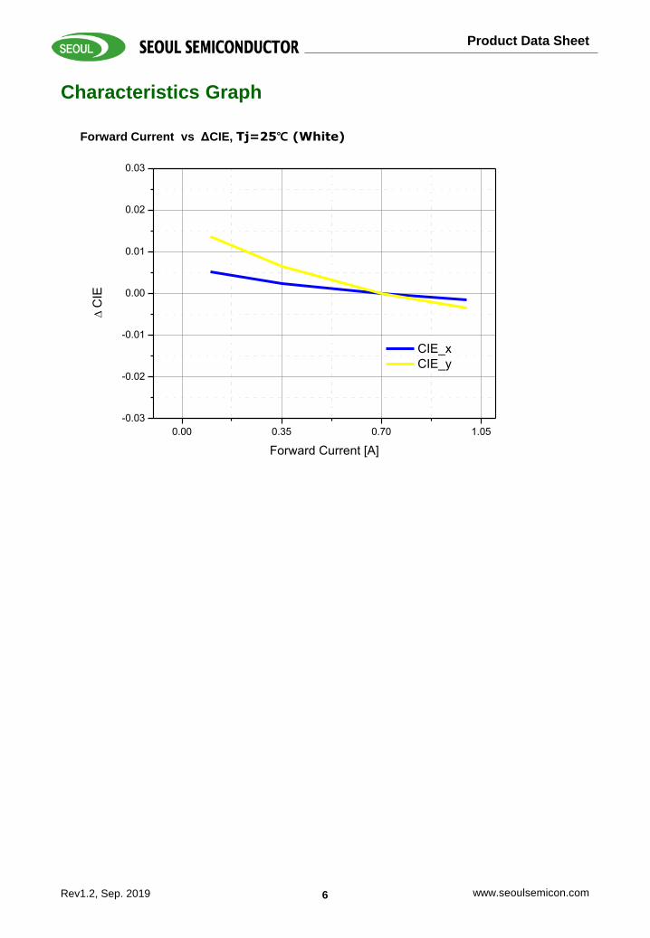
Forward Current vs ΔCIE, Tj=25℃ (White)
0.00 0.35 0.70 1.05
-0.03
-0.02
-0.01
0.00
0.01
0.02
0.03
CIE_x
CIE_y
C
IE
Forward Current [A]
0.00 0.35 0.70 1.05 1.40
0
100
200
300
400
500
600
700
Red
Green
Blue
White
Do
min
an
t W
ave
len
gth
[n
m]
Forward Current [A]
0.00 0.35 0.70 1.05 1.40
0.0
0.5
1.0
1.5
2.0
Red
Green
Blue
White
Re
lative
Ou
tpu
t[%
]
Forward Current [A]
0.00 0.35 0.70 1.05 1.40
0
100
200
300
400
500
600
700
Red
Green
Blue
White
Do
min
an
t W
ave
len
gth
[n
m]
Forward Current [A]0.00 0.35 0.70 1.05 1.40
-0.03
-0.02
-0.01
0.00
0.01
0.02
0.03
CIE_x
CIE_y
C
IE
Forward Current [A]
www.seoulsemicon.com7
Product Data Sheet
Rev1.2, Sep. 2019
Characteristics Graph
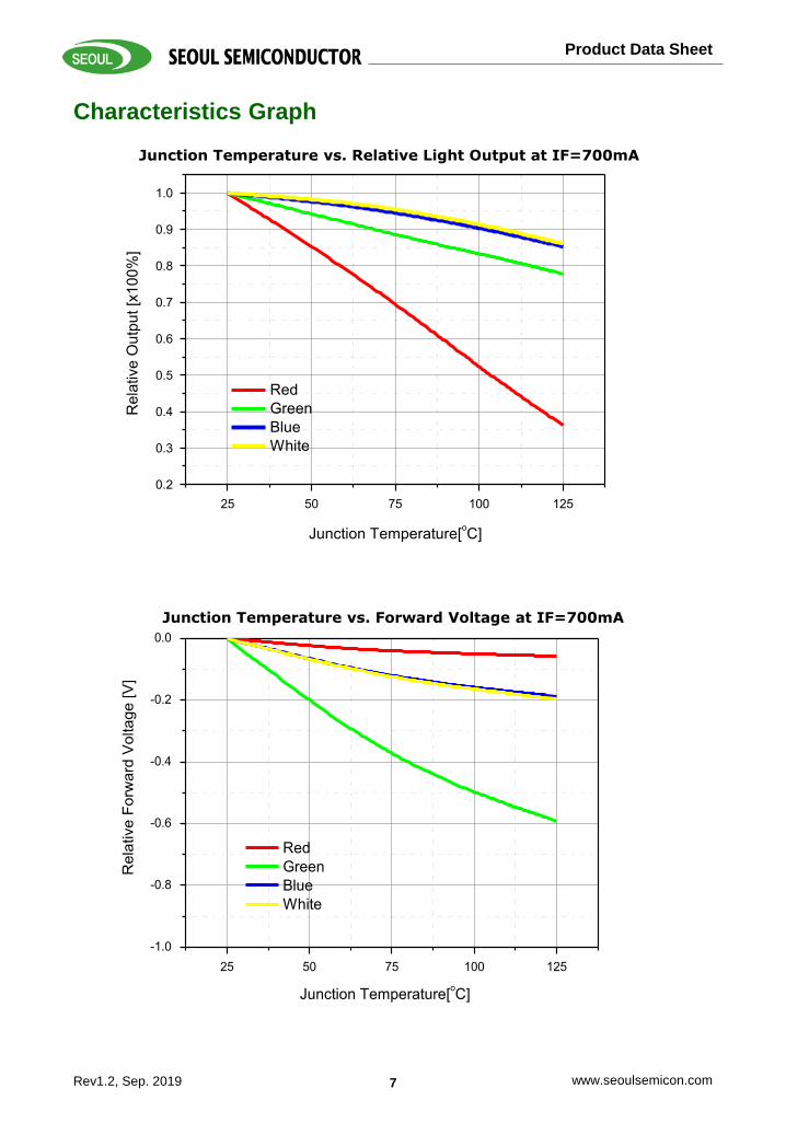
Junction Temperature vs. Relative Light Output at IF=700mA
Junction Temperature vs. Forward Voltage at IF=700mA
25 50 75 100 125
-1.0
-0.8
-0.6
-0.4
-0.2
0.0
Red
Green
Blue
White
Re
lative
Fo
rwa
rd V
olta
ge
[V
]
Junction Temperature[oC]
25 50 75 100 125
0.2
0.3
0.4
0.5
0.6
0.7
0.8
0.9
1.0
Red
Green
Blue
White
Re
lative
Ou
tpu
t [x
10
0%
]
Junction Temperature[oC]
25 50 75 100 125
0.4
0.5
0.6
0.7
0.8
0.9
1.0
Red
Green
Blue
White
Re
lative
Ou
tpu
t[%
]
Junction Temperature[oC]
25 50 75 100 125
0.2
0.3
0.4
0.5
0.6
0.7
0.8
0.9
1.0
Red
Green
Blue
White
Re
lative
Ou
tpu
t[%
]
Junction Temperature[oC]
40 60 80 100 120
-1.0
-0.8
-0.6
-0.4
-0.2
0.0
Red
Green
Blue
White
Re
lative
Fo
rwa
rd V
olta
ge
[V
]
Junction Temperature[oC]

www.seoulsemicon.com8
Product Data Sheet
Rev1.2, Sep. 2019
Characteristics Graph
Junction Temperature vs. Dominant Wavelength at IF=700mA
25 50 75 100 125
0
100
200
300
400
500
600
700
Junction Temperature[oC]
Red
Green
Blue
White
Do
min
an
t W
ave
len
gth
[n
m]
25 50 75 100 125
-0.04
-0.03
-0.02
-0.01
0.00
0.01
Junction Temperature[oC]
CIE_x
CIE_y
C
IE
Junction Temperature vs. White ΔCIE at IF=700mA

www.seoulsemicon.com9
Product Data Sheet
Rev1.2, Sep. 2019
Color Bin Structure
Table 3. Bin Code Description
Brightness IF = 700mA
Color Bin Flux [lm] Radiant Power [mW]
Red
RX 45 ~ 55 -
RY 55 ~ 70 -
RZ 70 ~ 90
RA 90 ~ 115
Green
GY 90 ~ 110 -
GZ 110 ~ 140 -
GA 140 ~ 180 -
Blue
BX - 600 ~ 700
BY - 700 ~ 800
BZ - 800 ~ 1,000
White
WZ 140 ~ 180 -
WA 180 ~ 230-
Wavelength IF = 700mA
Color BinDominant Wavelength
[nm]
GreenG1 519 ~ 525
G2 525 ~ 531
BlueB1 449 ~ 453
B2 453 ~458
0.295 0.300 0.305 0.310 0.315 0.320 0.325 0.330
0.29
0.30
0.31
0.32
0.33
0.34
0.35
0.36
CIE_x
CIE
_y AA
CIE IF = 700mA
Color CIE_x CIE_y
AA
(White)
0.3217 0.3558
0.3292 0.3418
0.3081 0.2990
0.2995 0.3132
www.seoulsemicon.com10
Product Data Sheet
Rev1.2, Sep. 2019
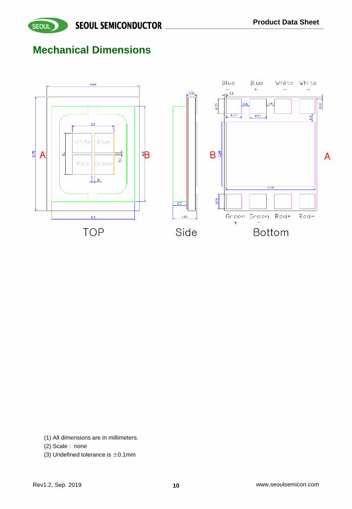
Mechanical Dimensions
(1) All dimensions are in millimeters.
(2) Scale : none
(3) Undefined tolerance is ±0.1mm
A B AB
www.seoulsemicon.com11
Product Data Sheet
Rev1.2, Sep. 2019
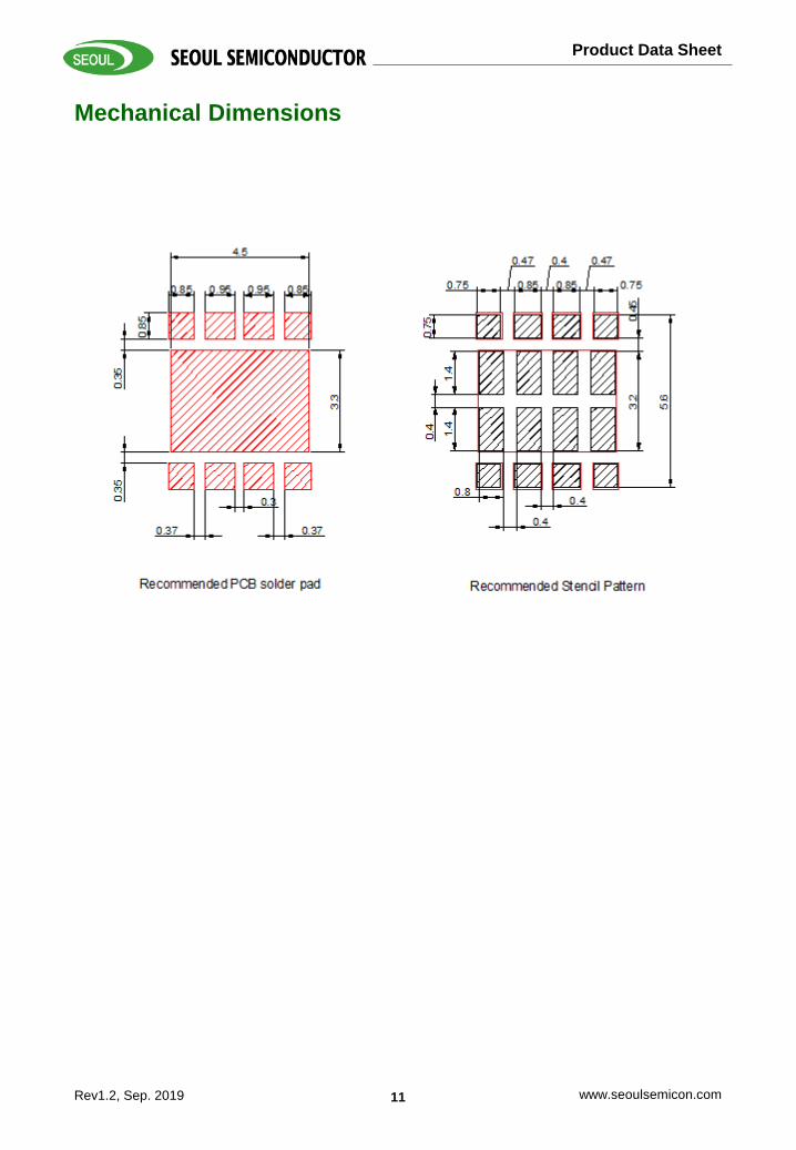
Mechanical Dimensions
www.seoulsemicon.com12
Product Data Sheet
Rev1.2, Sep. 2019
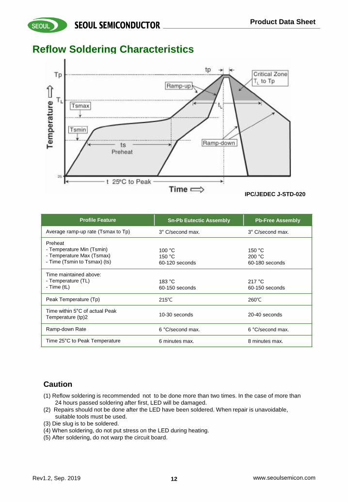
Reflow Soldering Characteristics
Caution
(1) Reflow soldering is recommended not to be done more than two times. In the case of more than
24 hours passed soldering after first, LED will be damaged.
(2) Repairs should not be done after the LED have been soldered. When repair is unavoidable,
suitable tools must be used.
(3) Die slug is to be soldered.
(4) When soldering, do not put stress on the LED during heating.
(5) After soldering, do not warp the circuit board.
IPC/JEDEC J-STD-020
Profile Feature Sn-Pb Eutectic Assembly Pb-Free Assembly
Average ramp-up rate (Tsmax to Tp) 3° C/second max. 3° C/second max.
Preheat
- Temperature Min (Tsmin)
- Temperature Max (Tsmax)
- Time (Tsmin to Tsmax) (ts)
100 °C150 °C60-120 seconds
150 °C200 °C60-180 seconds
Time maintained above:
- Temperature (TL)
- Time (tL)183 °C60-150 seconds
217 °C60-150 seconds
Peak Temperature (Tp) 215℃ 260℃
Time within 5°C of actual Peak
Temperature (tp)210-30 seconds 20-40 seconds
Ramp-down Rate 6 °C/second max. 6 °C/second max.
Time 25°C to Peak Temperature 6 minutes max. 8 minutes max.

www.seoulsemicon.com13
Product Data Sheet
Rev1.2, Sep. 2019
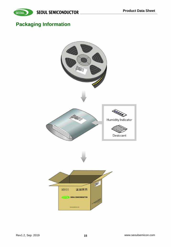
Emitter Tape & Reel Packaging
1. Quantity : 500pcs/Reel
2. Cumulative Tolerance : Cumulative Tolerance/10 pitches to be ±0.2mm
3. Adhesion Strength of Cover Tape : Adhesion strength to be 10-60g when the cover tape is
turned off from the carrier tape at the angle of 10º to the carrier tape
4. Package : P/N, Manufacturing data Code No. and quantity to be indicated on a damp proof
Package
Notes :
www.seoulsemicon.com14
Product Data Sheet
Rev1.2, Sep. 2019
Emitter Tape & Reel Packaging
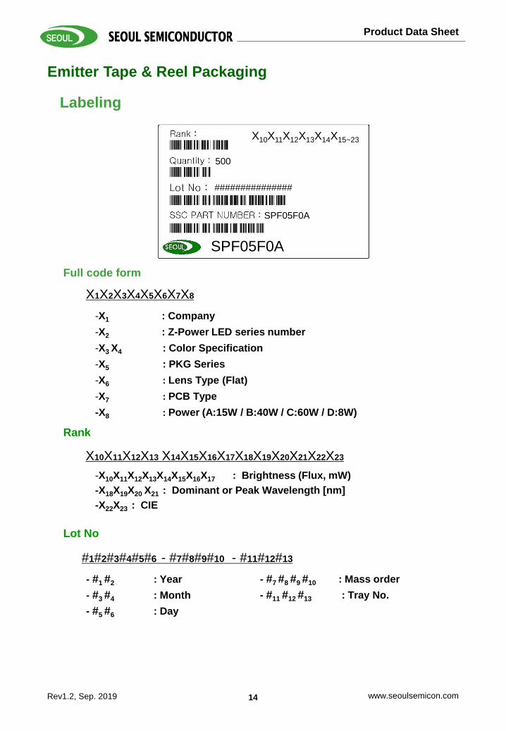
Labeling
-X10X11X12X13X14X15X16X17 : Brightness (Flux, mW)
-X18X19X20 X21 : Dominant or Peak Wavelength [nm]
-X22X23 : CIE
Rank
X10X11X12X13 X14X15X16X17X18X19X20X21X22X23
Lot No
#1#2#3#4#5#6 - #7#8#9#10 - #11#12#13
- #1 #2 : Year
- #3 #4 : Month
- #5 #6 : Day
- #7 #8 #9 #10 : Mass order
- #11 #12 #13 : Tray No.
500
###############
SPF05F0A
SPF05F0A
X10X11X12X13X14X15~23
X1X2X3X4X5X6X7X8
-X1 : Company
-X2 : Z-Power LED series number
-X3 X4 : Color Specification
-X5 : PKG Series
-X6 : Lens Type (Flat)
-X7 : PCB Type
-X8 : Power (A:15W / B:40W / C:60W / D:8W)
Full code form
www.seoulsemicon.com15
Product Data Sheet
Rev1.2, Sep. 2019
Packaging Information

www.seoulsemicon.com16
Product Data Sheet
Rev1.2, Sep. 2019
Color Bin StructureProduct Nomenclature
Part Number Code Description Part Number Value
X1 Company S Seoul Semiconductor
X2 Level of Integration 1 Discrete LED
X3X4 Technology C0 Color
X5X6X7X8 Dimension 4758 PKG size
X9X10 Power 15 W
X11X12 CRI 00
X13X14 Type 0000 Full / 1 Red / 2
Green / 3 Blue / 4 White
X15X16X17
Characteristic code
Flux Rank000
X18X19X20
Characteristic code
Vf Rank000
X21X22
Characteristic code
Color Step00
X23X24 Type 00
X25X26X27 Internal code 001
Part Numbering System
www.seoulsemicon.com17
Product Data Sheet
Rev1.2, Sep. 2019
Handling of Silicone Resin for LED
(1) During processing, mechanical stress on the surface should be minimized as much as possible.
Sharp objects of all types should not be used to pierce the sealing compound.
(2) In general, LED should only be handled from the side. By the way, this also applies to
LED without a silicone sealant, since the surface can also become scratched.
(3) When populating boards in SMT production, there are basically no restrictions regarding the form
of the pick and place nozzle, except that mechanical pressure on the surface of the resin must be
prevented. This is assured by choosing a pick and place nozzle which is larger than the LED’s
reflector area.
(4) Silicone differs from materials conventionally used for the manufacturing of LEDs. These
conditions must be considered during the handling of such devices. Compared to standard
encapsulants, silicone is generally softer, and the surface is more likely to attract dust. As
mentioned previously, the increased sensitivity to dust requires special care during processing. In
cases where a minimal level of dirt and dust particles cannot be guaranteed, a suitable cleaning
solution must be applied to the surface after the soldering of components.
(5) Seoul Semiconductor suggests using isopropyl alcohol for cleaning. In case other solvents are
used, it must be assured that these solvents do not dissolve the package or resin. Ultrasonic
cleaning is not recommended. Ultrasonic cleaning may cause damage to the LED.
(6) Please do not mold this product into another resin (epoxy, urethane, etc) and do not handle this
product with acid or sulfur material in sealed space.
(7) Avoid leaving fingerprints on silicone resin parts.

www.seoulsemicon.com18
Product Data Sheet
Rev1.2, Sep. 2019
Precaution for Use
(1) Storage
To avoid the moisture penetration, we recommend storing Z5 Series LED in a dry box with a
desiccant . The recommended storage temperature range is 5℃ to 30℃ and a maximum humidity of
RH50%.
(2) Use Precaution after Opening the Packaging
Use SMT techniques properly when you solder the LED as separation of the lens may affect the light
output efficiency.
Pay attention to the following:
a. Recommend conditions after opening the package
- Sealing / Temperature : 5 ~ 40℃ Humidity : less than RH30%
b. If the package has been opened more than 4 weeks (MSL 2a) or the color of
the desiccant changes, components should be dried for 10-12hr at 60±5℃
(3) Do not apply mechanical force or excess vibration during the cooling process to normal
temperature after soldering.
(4) Do not rapidly cool device after soldering.
(5) Components should not be mounted on warped (non coplanar) portion of PCB.
(6) Radioactive exposure is not considered for the products listed here in.
(7) Gallium arsenide is used in some of the products listed in this publication. These products are
dangerous if they are burned or shredded in the process of disposal. It is also dangerous to drink the
liquid or inhale the gas generated by such products when chemically disposed of.
(8) This device should not be used in any type of fluid such as water, oil, organic solvent and etc.
When washing is required, IPA (Isopropyl Alcohol) should be used.
(9) When the LED are in operation the maximum current should be decided after measuring the
package temperature.
(10) The appearance and specifications of the product may be modified for improvement without
notice.
(11) Long time exposure of sunlight or occasional UV exposure will cause lens discoloration.

www.seoulsemicon.com19
Product Data Sheet
Rev1.2, Sep. 2019
Precaution for Use
(12) VOCs (Volatile organic compounds) emitted from materials used in the construction of fixtures
can penetrate silicone encapsulants of LED and discolor when exposed to heat and photonic energy.
The result can be a significant loss of light output from the fixture. Knowledge of the properties of the
materials selected to be used in the construction of fixtures can help prevent these issues.
(13) Attaching LEDs, do not use adhesives that outgas organic vapor.
(14) The driving circuit must be designed to allow forward voltage only when it is ON or OFF. If the
reverse voltage is applied to LED, migration can be generated resulting in LED damage.
(15) LED is sensitive to Electro-Static Discharge (ESD) and Electrical Over Stress (EOS). Below is a
list of suggestions that Seoul Semiconductor purposes to minimize these effects.
a. ESD (Electro Static Discharge)
Electrostatic discharge (ESD) is the defined as the release of static electricity when two objects come
into contact. While most ESD events are considered harmless, it can be an expensive problem in
many industrial environments during production and storage. The damage from ESD to an LED may
cause the product to demonstrate unusual characteristics such as:
- Increase in reverse leakage current lowered turn-on voltage
- Abnormal emissions from the LED at low current
The following recommendations are suggested to help minimize the potential for an ESD event.
One or more recommended work area suggestions:
- Ionizing fan setup
- ESD table/shelf mat made of conductive materials
- ESD safe storage containers
One or more personnel suggestion options:
- Antistatic wrist-strap
- Antistatic material shoes
- Antistatic clothes
Environmental controls:
- Humidity control (ESD gets worse in a dry environment)
www.seoulsemicon.com20
Product Data Sheet
Rev1.2, Sep. 2019
Precaution for Use
b. EOS (Electrical Over Stress)
Electrical Over-Stress (EOS) is defined as damage that may occur when an electronic device is
subjected to a current or voltage that is beyond the maximum specification limits of the device.
The effects from an EOS event can be noticed through product performance like:
- Changes to the performance of the LED package
(If the damage is around the bond pad area and since the package is completely encapsulated
the package may turn on but flicker show severe performance degradation.)
- Changes to the light output of the luminaire from component failure
- Components on the board not operating at determined drive power
Failure of performance from entire fixture due to changes in circuit voltage and current across total
circuit causing trickle down failures. It is impossible to predict the failure mode of every LED exposed
to electrical overstress as the failure modes have been investigated to vary, but there are some
common signs that will indicate an EOS event has occurred:
- Damaged may be noticed to the bond wires (appearing similar to a blown fuse)
- Damage to the bond pads located on the emission surface of the LED package
(shadowing can be noticed around the bond pads while viewing through a microscope)
- Anomalies noticed in the encapsulation and phosphor around the bond wires.
- This damage usually appears due to the thermal stress produced during the EOS event.
c. To help minimize the damage from an EOS event Seoul Semiconductor recommends utilizing:
- A surge protection circuit
- An appropriately rated over voltage protection device
- A current limiting device

www.seoulsemicon.com21
Product Data Sheet
Rev1.2, Sep. 2019
Company Information
Published by
Seoul Semiconductor © 2013 All Rights Reserved.
Company Information
Seoul Semiconductor (www.SeoulSemicon.com) manufacturers and packages a wide selection of
light emitting diodes (LEDs) for the automotive, general illumination/lighting, Home appliance, signage
and back lighting markets. The company is the world’s fifth largest LED supplier, holding more than
10,000 patents globally, while offering a wide range of LED technology and production capacity in
areas such as “nPola”, "Acrich", the world’s first commercially produced AC LED, and "Acrich MJT -
Multi-Junction Technology" a proprietary family of high-voltage LEDs.
The company’s broad product portfolio includes a wide array of package and device choices such as
Acrich and Acirch2, high-brightness LEDs, mid-power LEDs, side-view LEDs, and through-hole type
LED as well as custom modules, displays, and sensors.
Legal Disclaimer
Information in this document is provided in connection with Seoul Semiconductor products. With
respect to any examples or hints given herein, any typical values stated herein and/or any information
regarding the application of the device, Seoul Semiconductor hereby disclaims any and all warranties
and liabilities of any kind, including without limitation, warranties of non-infringement of intellectual
property rights of any third party. The appearance and specifications of the product can be changed
to improve the quality and/or performance without notice.