spin injection hall effect: a new member of the spintronic hall family and its implications in...
Post on 20-Dec-2015
217 views
TRANSCRIPT

Spin Injection Hall Effect: a new member of the spintronic Hall family and
its implications in nano-spintronics
Research fueled by:
Optical Spintronics MeetingHitachi-Cambridge,October 27th, 2009
JAIRO SINOVATexas A&M University
Institute of Physics ASCR
Hitachi CambridgeJoerg Wunderlich, X. Xu,
A. Irvine, et al
Institute of Physics ASCRTomas Jungwirth, Vít Novák, et al
Texas A&M L. Zarbo

2Nanoelectronics, spintronics, and materials control by spin-orbit coupling
Can we achieve direct spin polarization injection, detection, and manipulation by electrical means in an all paramagnetic semiconductor system?
Long standing paradigm: Datta-Das FET
Unfortunately it has not worked :•no reliable detection of spin-polarization in a diagonal transport configuration •No long spin-coherence in a Rashba spin-orbit coupled system
Towards a REALISTIC spin-based non-magnetic FET device
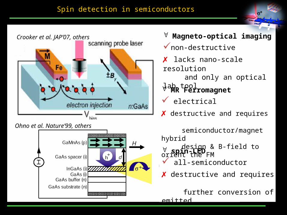
Ohno et al. Nature’99, others
Crooker et al. JAP’07, others Magneto-optical imaging
non-destructive
lacks nano-scale resolution and only an optical lab tool
MR Ferromagnet
electrical
destructive and requires semiconductor/magnet hybrid design & B-field to orient the FM
spin-LED
all-semiconductor
destructive and requires further conversion of emitted light to electrical signal
Spin detection in semiconductors

4
SHEB=0
charge current gives
spin current
Optical detection
SHE-1
B=0spin current
gives charge current Electrical
detection
js–––––––––––
+ + + + + + + + + +iSHEI
_ FSO
FSO
_ __
majority
minority
V
The family of spintronic Hall effects
AHEB=0
polarized charge current gives charge-spin
current
Electrical detection
J. Wunderlich, B. Kaestner, J. Sinova andT. Jungwirth, Phys. Rev. Lett. 94 047204 (2005)
Spin-Hall Effect
5
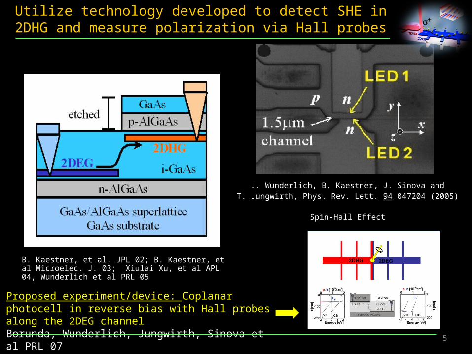
B. Kaestner, et al, JPL 02; B. Kaestner, et al Microelec. J. 03; Xiulai Xu, et al APL 04, Wunderlich et al PRL 05
Proposed experiment/device: Coplanar photocell in reverse bias with Hall probes along the 2DEG channelBorunda, Wunderlich, Jungwirth, Sinova et al PRL 07
Utilize technology developed to detect SHE in 2DHG and measure polarization via Hall probes

i pn
2DHG
Device schematics: materials
-
2DHGi p
n
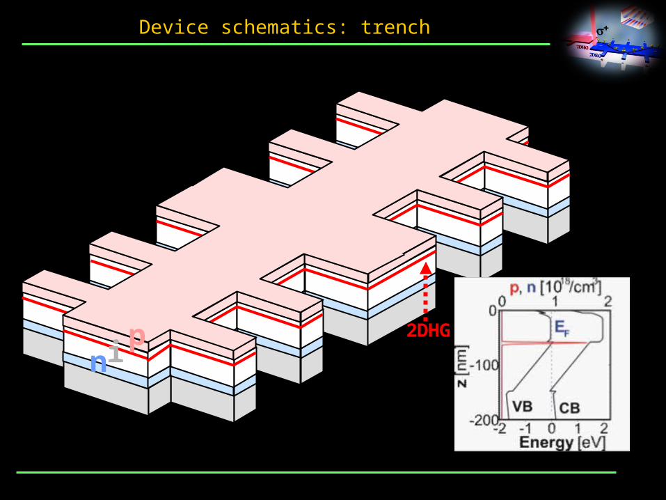
Device schematics: trench

i
p
n2DHG
2DEG
Device schematics: n-etch

Vd
VH
2DHG
2DEG
Vs
9
Device schematics: materials

2DHG
2DEG
e
h
ee
ee
e
hh
h
h h
Vs
Vd
VH
10
Device schematics: SIHE measurement

11Nanoelectronics, spintronics, and materials control by spin-orbit coupling
2DHG
2DEG
e
h
ee
ee
e
hhh
h h
Vs
Vd
VH
Spin-injection Hall effect device schematics

12Nanoelectronics, spintronics, and materials control by spin-orbit coupling
Spin-injection Hall device measurements
trans. signal
σσooσσ++σσ-- σσoo
VL
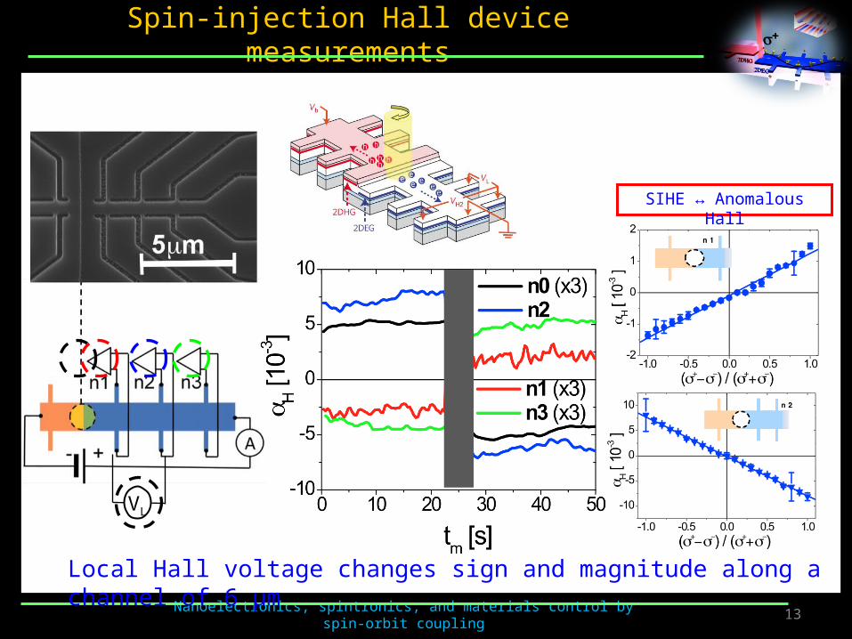
13Nanoelectronics, spintronics, and materials control by spin-orbit coupling
Spin-injection Hall device measurements
trans. signal
σσooσσ++σσ-- σσoo
VL
SIHE ↔ Anomalous Hall
Local Hall voltage changes sign and magnitude along a channel of 6 μm
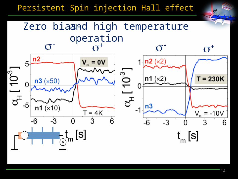
and high temperature operation
Zero bias-
σ+σ- σ+σ-
14
Persistent Spin injection Hall effect

15Nanoelectronics, spintronics, and materials control by spin-orbit coupling
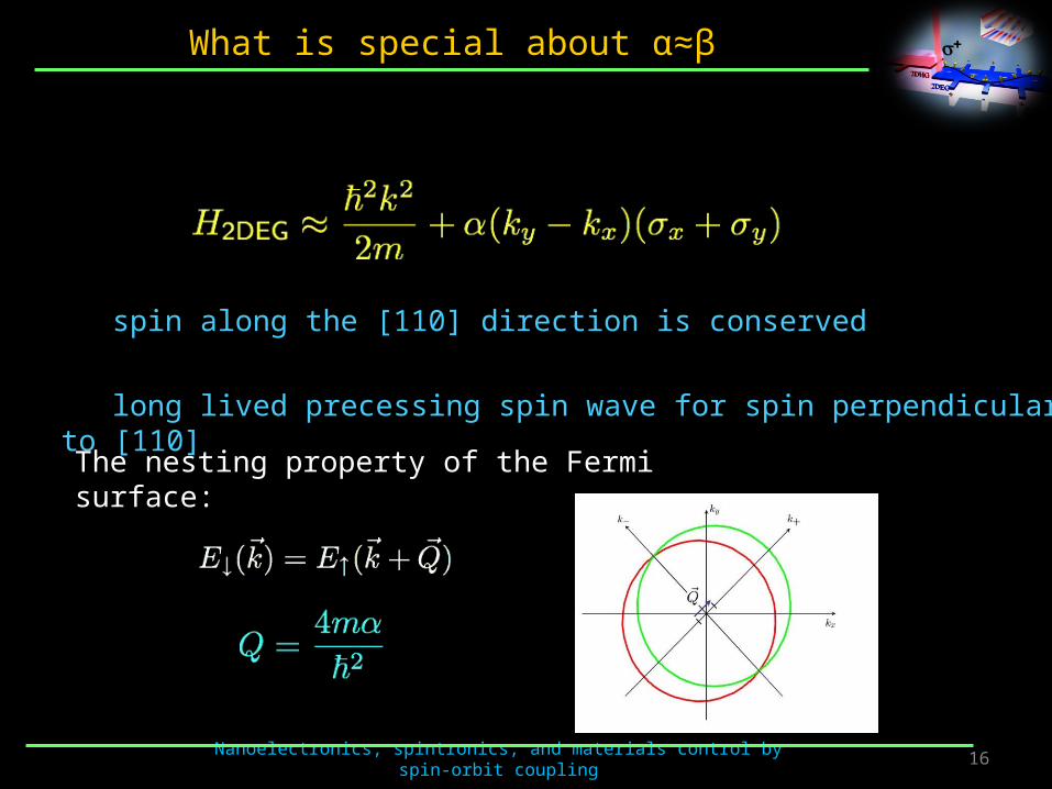
Spin-dynamics in 2D electron gas with Rashba and Dresselhauss SO coupling
The 2DEG is well described by the effective Hamiltonian:
Hence
For our 2DEG system:
16Nanoelectronics, spintronics, and materials control by spin-orbit coupling
What is special about α≈β
• spin along the [110] direction is conserved
• long lived precessing spin wave for spin perpendicular to [110]
The nesting property of the Fermi surface:

17Nanoelectronics, spintronics, and materials control by spin-orbit coupling
Effects of Rashba and Dresselhaus SO coupling
α= -β
[110]
[110]_
ky [010]
kx [100]
α > 0, β = 0[110]
[110]_
ky [010]
kx [100]
α = 0, β < 0[110]
[110]_
ky [010]
kx [100]

18Nanoelectronics, spintronics, and materials control by spin-orbit coupling
Spin-dynamics in 2D systems with Rashba and Dresselhauss SO coupling
For the same distance traveled along [1-10], the spin precesses by exactly the same angle.
[110]
[110]_
[110]_

19Nanoelectronics, spintronics, and materials control by spin-orbit coupling
Similar wafer parameters to ours
Persistent state spin helix verified by pump-probe experiments
Weber et al. PRL 07

For arbitrary α,β spin-charge transport equation is obtained for diffusive regime
For propagation on [1-10], the equations decouple in two blocks. Focus on the one coupling Sx+ and Sz:
For Dresselhauss = 0, the equations reduce to Burkov, Nunez and MacDonald, PRB 70, 155308 (2004);
Mishchenko, Shytov, Halperin, PRL 93, 226602 (2004)
20
The Spin-Charge Drift-Diffusion Transport Equations

21Nanoelectronics, spintronics, and materials control by spin-orbit coupling
Spatial variation scale consistent with the one observed in SIHE
Spin-helix state when α ≠ β
22Nanoelectronics, spintronics, and materials control by spin-orbit coupling
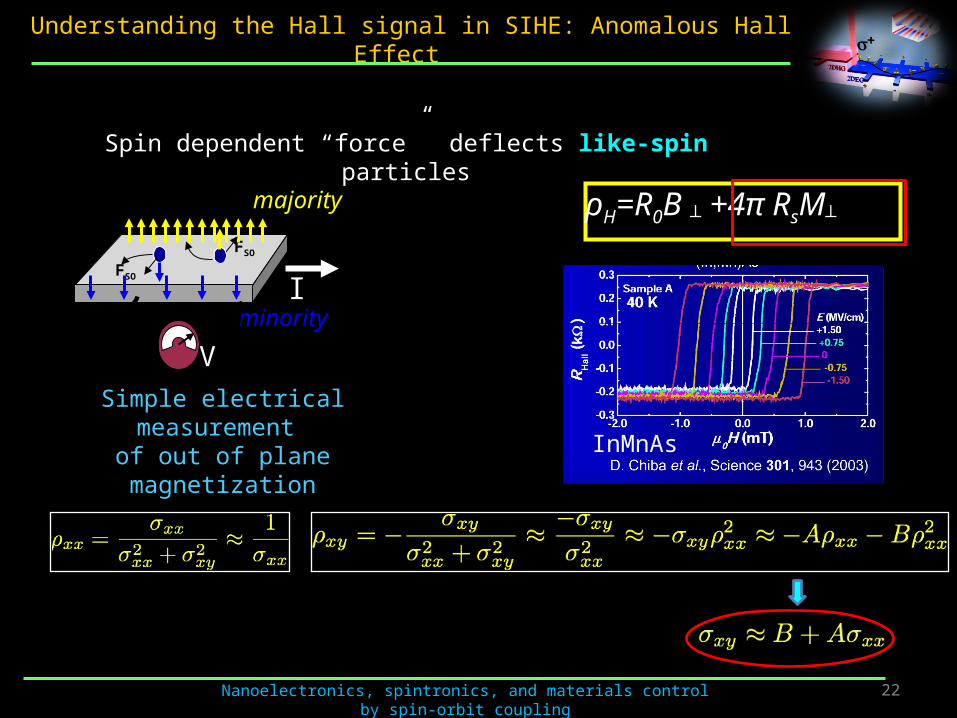
Simple electrical measurement of out of plane magnetization
InMnAs
I
FSO
FSO
majority
minority
V
Spin dependent “force” deflects like-spin particles
ρH=R0B ┴ +4π RsM┴
Understanding the Hall signal in SIHE: Anomalous Hall Effect
23Nanoelectronics, spintronics, and materials control by spin-orbit coupling
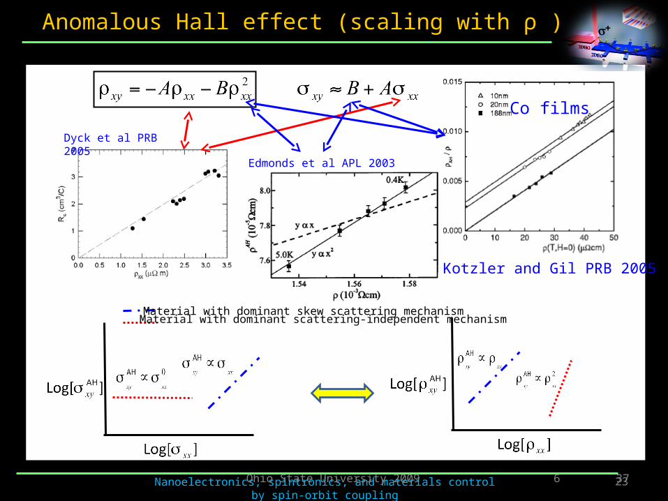
Anomalous Hall effect (scaling with ρ )
37
Dyck et al PRB 2005
Material with dominant skew scattering mechanismMaterial with dominant scattering-independent mechanism
Ohio State University 2009 6
GaMnAs
Kotzler and Gil PRB 2005
Co films
Edmonds et al APL 2003
24Nanoelectronics, spintronics, and materials control by spin-orbit coupling
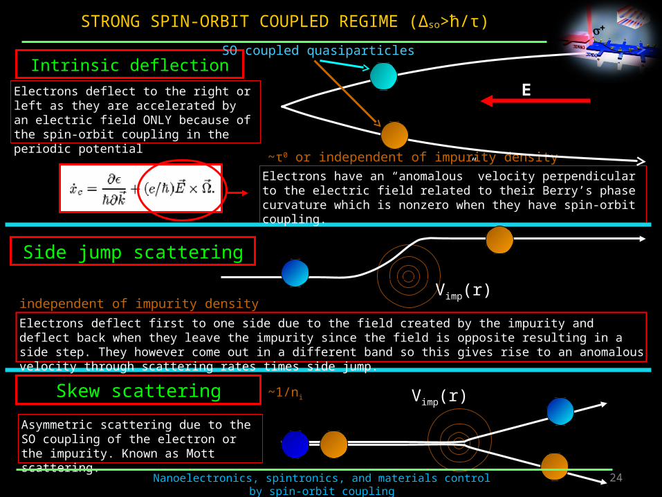
Intrinsic deflection
Electrons have an “anomalous” velocity perpendicular to the electric field related to their Berry’s phase curvature which is nonzero when they have spin-orbit coupling.
~τ0 or independent of impurity density
Electrons deflect first to one side due to the field created by the impurity and deflect back when they leave the impurity since the field is opposite resulting in a side step. They however come out in a different band so this gives rise to an anomalous velocity through scattering rates times side jump.
independent of impurity density
Side jump scattering
Vimp(r)
Skew scattering
Asymmetric scattering due to the SO coupling of the electron or the impurity. Known as Mott scattering.
~1/ni Vimp(r)
Electrons deflect to the right or left as they are accelerated by an electric field ONLY because of the spin-orbit coupling in the periodic potential
E
SO coupled quasiparticles
STRONG SPIN-ORBIT COUPLED REGIME (Δso>ħ/τ)

25Nanoelectronics, spintronics, and materials control by spin-orbit coupling
Side jump scattering from SO disorder
Electrons deflect first to one side due to the field created by the impurity and deflect back when they leave the impurity since the field is opposite resulting in a side step. They however come out in a different band so this gives rise to an anomalous velocity through scattering rates times side jump.
independent of impurity density
The terms/contributions dominant in the strong SO couple regime are strongly reduced (quasiparticles not well defined due to strong disorder broadening). Other terms, originating from the interaction of the quasiparticles with the SO-coupled part of the disorder potential dominate.
Better understood than the strongly SO couple regime
WEAK SPIN-ORBIT COUPLED REGIME (Δso<ħ/τ)
Skew scattering from SO disorder
~1/ni
26Nanoelectronics, spintronics, and materials control by spin-orbit coupling
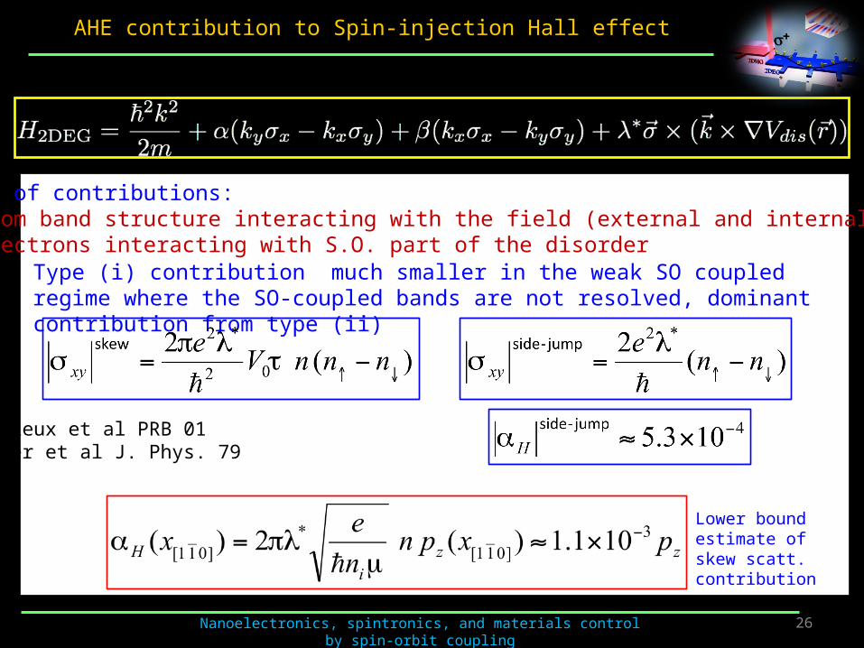
Type (i) contribution much smaller in the weak SO coupled regime where the SO-coupled bands are not resolved, dominant contribution from type (ii)
Crepieux et al PRB 01Nozier et al J. Phys. 79
Two types of contributions: i)S.O. from band structure interacting with the field (external and internal)•Bloch electrons interacting with S.O. part of the disorder
Lower bound estimate of skew scatt. contribution
AHE contribution to Spin-injection Hall effect

27Nanoelectronics, spintronics, and materials control by spin-orbit coupling
Local spin-polarization → calculation of AHE signal
Weak SO coupling regime → extrinsic skew-scattering term is dominant
Lower bound estimate
Spin-injection Hall effect: theoretical expectations

28Nanoelectronics, spintronics, and materials control by spin-orbit coupling
Further experimental tests of the observed SIHE

S. Datta, B. Das,Appl. Phys. Lett. 56 665 (1990).
… works only
- if channel is 1dimensional
- or under Spin Helix conditions for 2D channel
Comment 1: Datta-Das type device

SIHE Field Effect Transistor

31Nanoelectronics, spintronics, and materials control by spin-orbit coupling
SHE-1
B=0spin current gives
charge current
Electrical detection
AHEB=0
polarized charge current gives charge-spin
current
Electrical detection
SHEB=0
charge current gives spin current
Optical detection
SIHEB=0
Optical injected polarized current
gives charge current
Electrical detection
The spintronic Hall family

32
- electrical detection method for Spin current
- large signal (comparable to AHE in metallic ferromagnets)
- high spatial resolution (~ < 50nm)
- nondestructive detection of spin WITHOUT magnetic elements
- linear with degree of spin polarization
- high temperature operation
- first electrical detection of the Spin Helix (coherently precessing spins)
- all electrical polarimeter (transfers degree of light polarization into an electrical signal)
SUMMARY
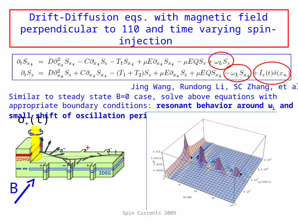
Drift-Diffusion eqs. with magnetic field perpendicular to 110 and time varying spin-injection
Spin Currents 2009
σ+(t)
B
Similar to steady state B=0 case, solve above equations with appropriate boundary conditions: resonant behavior around ωL and small shift of oscillation period
Jing Wang, Rundong Li, SC Zhang, et al

Semiclassical Monte Carlo of SIHENumerical solution of Boltzmann equation
Spin-independent scattering:
Spin-dependent scattering:
•phonons,•remote impurities,•interface roughness, etc.
•side-jump, skew scattering.
AHE
•Realistic system sizes (μm).•Less computationally intensive than other methods (e.g. NEGF).
Spin Currents 2009

Single Particle Monte Carlo
Spin Currents 2009
Spin-Dependent Semiclassical Monte CarloTemperature effects, disorder, nonlinear effects, transient regimes.Transparent inclusion of relevant microscopic mechanisms affecting spin transport (impurities, phonons, AHE contributions, etc.).Less computationally intensive than other methods(NEGF).Realistic size devices.

Effects of B field: current set-up
Spin Currents 2009
In-Plane magnetic fieldOut-of plane magnetic field