spmv: a memory-bound application on the gpu stuck between … · 2017-09-16 · spmv multicore...
TRANSCRIPT

SpMV: A Memory-Bound Application on the GPUStuck Between a Rock and a Hard Place
John D. Davis and Eric S. ChungMicrosoft Research Silicon Valley{joda, erchung}@microsoft.com
Abstract—In this paper, we investigate the relative meritsbetween GPGPUs and multicores in the context of sparsematrix-vector multiplication (SpMV). While GPGPUs possessimpressive capabilities in terms of raw compute throughputand memory bandwidth, their performance varies significantlywith application tuning as well as sparse input and formatcharacteristics. Furthermore, several emerging technological andworkload trends potentially shift the balance in favor towardsthe multicore, especially in the context of bandwidth-limitedworkloads. In light of these trends, our paper investigates theperformance, power, and cost of state-of-the-art GPGPUs andmulticores across a spectrum of sparse inputs. Our resultsreinforce some current-day understandings of GPGPUs andmulticores while offering new insights on their relative meritsin the context of future systems.
I. INTRODUCTION
Sparse matrix-vector multiplication (SpMV) is a criticalkernel employed in many high performance computing (HPC)applications. SpMV is a dominant component of iterativemethods that solve large-scale linear systems and eigenvalueproblems. The widespread importance of SpMV has resulted insignificant research efforts poured into optimizing the kernel’sperformance on modern-day multicores and general-purposeGPU (GPGPU) platforms (e.g., [1, 2]). Standard libraries suchas Intel’s MKL [3] and Nvidia’s CUBLAS [4] and Cusp [1]provide users with highly tuned SpMV implementations de-signed to maximize core efficiency and memory bandwidth.
In this paper, we investigate the relative merits between mul-ticores and GPGPUs when optimizing a commodity systemfor performance under approximately equal power and costconstraints. A recurring claim that has been made in recentyears is that GPGPUs offer significant performance advan-tages over conventional multicores, especially with respectto SpMV [1]. Proponents highlight the GPGPU’s advantagein memory bandwidth and its abundance of floating pointcores. For some sparse matrices, GPGPUs achieve over 4Xthroughput improvement over the multicore in previouslyconducted studies [1].
Are GPGPUs Worth The Effort? Despite the impressiveraw capabilities of GPGPUs, such performance gains areachievable only when extensive tuning efforts are employedand when certain sparse inputs are regular and amenable toload-balancing. Furthermore, we have begun to observe severalemerging technological and workload trends that potentiallymitigate these benefits: (1) the convergence of memory band-width between CPUs and GPGPUs, (2) increasing last-level
cache sizes of multicores, and (3) the trends towards large-scale inputs (i.e., “big data”).
Contributions. In this paper, we re-examine the GPGPU’s ad-vantage over conventional multicores and investigate whetherthe increased programmability burden and tuning are justifi-able in the context of building a system with approximatelyequal cost and power budgets. To conduct our investigations,we perform detailed performance and power measurementsof state-of-the-art platforms using GPGPUs and multicores.From our experimental measurements, we derive several ob-servations:
• For SpMV, GPGPU performance has stagnated in recentarchitecture generations, despite extensive tuning effortsby the research community.
• In general, GPGPUs achieve high speedups over themulticore on input set sizes that exceed the multicore’slast-level cache, but do not exceed the GPGPU’s externalDRAM capacity.
• SpMV multicore performance has been gaining on theGPU in recent years due to improved memory bandwidthin commodity multicore systems.
• To the first order, a dual-socket multicore is sufficient toreplace a single GPGPU assuming approximately equalcost and power consumption.
• When extrapolated to future technological trends, theadvantages of using GPGPUs for SpMV diminishes sig-nificantly as multicores are able to catch up in bandwidth-limited performance.
Outline. The remainder of this paper is as follows. Section IIdiscusses key technological trends that motivate this work.Section III describes background and related work. Section IVelaborates on the experimental setup used to conduct ourstudies. Section V discusses in detail the experimental results.Section VII offers conclusions and future work.
II. MOTIVATION AND TRENDS
Over the last several years, researchers and applicationdevelopers have poured an immense amount of effort intothe programmability, tuning, and demonstration of general-purpose graphic processors (GPGPUs). In contrast to conven-tional multicores, GPGPUs offer substantial peak computa-tional throughput (on the order of teraflops/sec) and high mem-ory bandwidth (nearly up to 200 GB/sec). GPGPUs achievegood performance and efficiency by relying on hundreds, if

1
10
100
1000
Q1
'20
00
Q1
'20
01
Q1
'20
02
Q1
'20
03
Q1
'20
04
Q1
'20
05
Q1
'20
06
Q1
'20
07
Q1
'20
08
Q1
'20
09
Q1
'20
10
Q1
'20
11
Q1
'20
12
Ban
dw
idth
(G
B/s
)
Time (Quarters)
CPU and GPU Memory Bandwidth vs. Time
Dual XeonDual OpteronNvida GPUATI GPU
8X 4X
1.6–2.2X
Fig. 1. Bandwidth Gap between GPGPUs vs. CPUs.
not thousands of threads to extract parallelism from a targetapplication.
Recently, emerging technological trends are calling intoquestion as to whether GPGPUs are “always the right an-swer” when high performance is of utmost demand. Unlikeconventional processors, GPGPU applications are considerablyfragile and require extensive tuning to maximize effectiveness.In the case of Sparse Matrix-Vector Multiplication (SpMV),we are particularly interested in knowing whether well-tunedGPGPUs today (and moving forward into the future) willprovide a significant enough performance (or energy) benefitto justify their complex tuning and programming requirements.
Bandwidth Trends. A potential threat to the GPGPU’s dom-inance is the fact that conventional multicores are closing thegap in performance and bandwidth. As Figure 1 shows, thememory bandwidth gap between GPGPUs and multicores hasbeen shrinking over the last five years. As recently as 2012,a high-end dual-socket Xeon system can achieve over 100GB/sec of memory bandwidth, a level difficult to envision fiveyears ago.
The remaining advantage of the GPGPU over CPU isnow the raw processing throughput that compute-bound ap-plications can exploit. However, in many memory-bound ap-plications such as SpMV, it becomes increasingly unclearwhether GPGPUs can still offer a significant advantage. Inparticular, SpMV is classified as an irregular memory accessapplication, which must be optimized along the followingaxes: (1) memory efficiency, (2) load balancing, and (3) threadutilization. This requires careful mapping and data marshalingto support the desired computational throughput. Althoughconventional multicores suffer similar problems, the developeris responsible for managing far less complexity than in theGPGPU (tens of threads vs. thousands). Furthermore, conven-tional multicores also contain large last-level caches (20MBor more) that automatically improve memory efficiency.
Memory Capacity Trends. In addition to increased band-width, the last-level caches of multicores continue to growunabated. The Intel Sandy Bridge architecture [5] enables upto 20MB of on-die cache, or 40MB in a dual-socket Xeon
1.E+00
1.E+01
1.E+02
1.E+03
1.E+04
1.E+05
1.E+06
1.E+07
1.E+08
1.E+09
1.E+10
1.E+11
1
11
1
22
1
33
1
44
1
55
1
66
1
77
1
88
1
99
1
11
01
12
11
13
21
14
31
15
41
16
51
17
61
18
71
19
81
20
91
22
01
23
11
24
21
Me
mo
ry F
oo
tpri
nt
(Byt
es)
Sparse Matrices from Univ. Florida Sparse Collection
Sparse Matrix Memory Footprint
2547 Sparse Matrices
Fits in Multicore Last-level Cache
Exceeds GPGPU RAM Capacity
Optimal GPGPU Region
Fig. 2. Sparse Matrix Memory Footprint.
configuration [5]. The successor architecture, Ivy Bridge, canexpect up to 32MB of last-level cache per die. In contrast,an Nvidia GPGPU provides only a scant amount of cache,on the order of a megabyte or less [6]. An interestingconsequence of having massive caches in the multicore isthe impact on traditional “memory-bound” iterative solvers.Across a collection of 2,547 real-world sparse matrices fromthe University of Florida Sparse Collection [7], 93% of thematrices can fit entirely in the 40 MB cache (not includingmetadata overhead), which ultimately negates the benefit ofhaving extremely high external bandwidth, as in the case of theGPGPU. Figure 2 plots each of the individual matrices againstthe total memory footprint. The lower horizontal bar indicatesthe last-level cache size of a Sandy Bridge-based Dual-SocketXeon, while the upper horizontal bar indicates the maximumGDDR capacity of an Nvidia GTX680 GPGPU.
Long-Term Hypothesis. Based on Figure 2, we project thatfuture “big data” trends will ultimately limit the utility ofrunning SpMV on GPGPUs, which must either constrain theirinputs to limited off-chip memory or must reload their dataover a slow PCIe bus, destroying any of the benefits that GPG-PUs may provide. Furthermore, the favorable regions whereGPGPUs can excel at will be gradually subsumed by morecapable CPUs, while larger data sets will push such workloadsout of reach of the memory-constrained GPGPUs1. In the nextsection, we will provide background knowledge on the SpMVkernel and various CPU and GPGPU implementations. Thissection is followed by an experimental study used to test ourlong-term hypothesis.
III. SPARSE MATRIX-VECTOR MULTIPLICATION
Sparse Matrix-Vector Multiplication is a highly exercisedscientific kernel that solves y = Ax, where x and y are densevectors, while A is a sparse matrix. In iterative methods, theSpMV kernel is typically executed thousands of times beforeconvergence is reached. To avoid excessive waste in bandwidth
1Or stuck between a rock and a hard place.

and storage, the sparse matrix A is typically encoded usinga sparse format, which stores only the non-zero values ofthe matrix along with meta-data that identifies a non-zero’slocation in the matrix.
Using the right sparse matrix format is essential becauseat runtime, the metadata must be decoded for each non-zero,which is used to identify the corresponding x vector value forcalculating the dot product. A major challenge in computingy = Ax is the irregularity of accesses to the x vector as aresult of the non-zero access patterns in the matrix.
It is notable that GPGPUs are very sensitive to the sparsematrix format. The format and resulting metadata can impactthe load balance, resource utilization, and memory efficiency.As Bell and Garland showed, an “improper” sparse matrixformat can degrade performance by an order of magnitude ormore [8].
Sparse Formats. A wide variety of sparse formats exist,trading storage/bandwidth and processing overhead. Coordi-nate (COO), Compressed Sparse Row (CSR), and ELLPACK(ELL) are common formats supported by standard sparsematrix packages like SPARSKIT [9]. Figure 3 illustrates theseformats for an example sparse matrix. The COO format is thesimplest, where each row and column index is stored alongwith the non-zero value. In the CSR format, the row arrayis replaced by pointers that demarcate the beginning of rowswithin the column array. Finally, in the ELL format, the entiresparse matrix is packed into a dense matrix with dimensionk, where k is the largest number of non-zeros amongst all therows. A secondary dense matrix encodes the column index foreach respective nonzero. ELL format is most well-suited forvector architectures because of its fixed length rows.
Table I provides a summary of revelant details of some ofthe matrices used in this and other studies. We also profiled theentire University of Florida Sparse Matrix Collection to under-stand the storage ramifications of these popular formats. Onthe right of the table, we normalize the storage requirementsto the most common format, CSR. In general, COO is themost stable format compared to CSR, having low overheadand a low standard deviation. For matrices with a uniformnumber of nonzero values, ELL can be the most storageefficient, because there is no need to store row metadata.It also can experience massive amounts of overhead due todata and metadata padding for matrices with very skewednonzero distributions. Finally, Bell and Garland derived theirown format, a combination of ELL for the bulk of the matrixand COO to store the remaining rows with a large numberof nonzeros [8]. On average, this format sacrifices storageefficiency relative to CSR and COO, with a focus on improvingGPGPU performance.
Multicore Optimizations. A substantial body of literature hasexplored the optimization of sparse formats and algorithmsfor single-core and multi-core processors (e.g., [10, 11, 2,9, 12, 13]). In general, many optimizations aim to minimizethe irregularity of the matrix structure by selecting a formatbest suited for the matrix kernel. Commercial libraries such
Matrix
1 0 4 03 7 0 00 0 2 95 8 0 7
COO
row =
indices =
data =
[0 2 0 1 2 3 0 1 3]
[1 4 3 7 2 9 5 8 7]
[0 0 1 1 2 2 3 3 3]
data indices
1 4 *3 7 * 2 9 *5 8 7
0 2 * 0 1 *2 3 *0 1 3
ptr =indices =
data =
[0 2 4 6 9]
[0 2 0 1 2 3 0 1 3]
[1 4 3 7 2 9 5 8 7]
CSR
ELL
Fig. 3. Various Formats Used to Encode Sparse Matrices.
as Intel MKL provide optimized SpMV libraries for Intel-based processors. In processor-based systems, multithreading,SSE instructions, cache blocking and mitigation of x-vectorirregularity are common techniques used to boost the effi-ciency and performance of SpMV. The use of auto-tuning hasalso been shown to be an effective technique for selectinggood optimizations for a given processor’s configuration andplatform [2].
GPGPU Optimizations. In the space of GPGPUs, a sig-nificant body of work exists on creating specialized dataformats that mitigate load-balance issues. The performanceof SpMV on GPGPUs is particularly sensitive to the formatused to encode the matrix. An ELL format, for example,presents a simple array-based structure that simplifies load-balancing and scheduling on the GPGPU. However, ELL alsoincurs substantial waste if there is significant variability in thenumber of non-zeros per row [1]. A corollary to the format’sperformance is its storage and bandwidth requirements. Asshown in Table I, the storage requirements on the GPGPU canalso impact performance. In our evaluations that compare theGTX680 and GTX580, there existed several large matrices thatfit in the memory of the GPGPUs in one format, but not theother. In some cases, the GTX680 was able to exploit a givenformat because of its large memory, whereas the GTX580could not. The same holds true when comparing CPU andGPGPU performance. We will later present a few examplesof the CPU’s performance being artificially inflated becausethe GPGPU does not have the memory capacity for the fasterformat.
Related Work. Related to CPUs and GPGPUs, we build onthe auto-tuning results of Williams et al. [2] and the cusplibrary as discussed by Bell and Garland [8]. We extend theirwork based on the narrowing bandwidth gap and investigatenewer CPU and GPU architectures. We measure both perfor-mance and power using the last version of their code [1] andacross a spectrum of inputs that vary the impact of the last-level cache [7]. Likewise, Lee et al. [14] presents performanceresults demonstrating the narrowing performance gap across awide range of workloads, but omit any power comparisons.From this work and our experience, tuning and debuggingthe GPGPU is significantly more challenging than CPUs. Inparticular, we noticed a significant amount of variability inperformance with respect to the format and data set size.

matrix rows cols nonzeros % nonzeros CSR COO ELL HYB
Inputs used in [8]
dense 32,768 32,768 1073741824 100 % 1.0 1.33 1.00 1.50
cant 62451 62451 4007383 0.10% 1.0 1.33 1.21 1.75conf5 0-4x4(qcd) 3072 3072 119808 1.27% 1.0 1.32 0.99 1.32conf5 4-8x8 (qcd) 49152 49152 1916928 0.08% 1.0 1.32 0.99 1.32consph 83334 83334 6010480 0.09% 1.0 1.33 1.12 1.82cop20k A 121192 121192 2624331 0.02% 1.0 1.31 3.68 1.99epb1 14734 14734 95053 0.04% 1.0 1.27 1.03 1.54mac econ fwd500 206500 206500 1273389 2.99e-3% 1.0 1.26 6.77 1.64mc2depi 525825 525825 2100225 7.60e-4% 1.0 1.23 0.92 1.92pdb1HYS 36417 36417 4344765 0.33% 1.0 1.33 1.71 1.82pwtk 217918 217918 11634424 0.02% 1.0 1.33 3.35 1.53rail4284 4284 1096894 11284032 0.24% 1.0 1.33 21.3 1.34rma10 46835 46835 2374001 0.11% 1.0 1.32 2.84 1.79scircuit 170998 170998 958936 3.28e-3% 1.0 1.26 59.4 1.52shipsec1 140874 140874 3977139* 0.04% 1.0 1.33 1.83 1.66webbase-1M 1000005 1000005 3105536 3.11e-4% 1.0 1.20 1366 1.49
All sparse matrices [7]
Mean 361922 361132 4448472 1.82% 1.0 1.26 390 1.46Median 4182 5300 40424 0.23% 1.0 1.27 2.77 1.31Stdev 3339878 3333546 55947269 6.10% 1.0 0.06 6092 0.32Min 2 3 3 2.09e-6% 1.0 0.85 0.55 0.85Max 118142142 118142155 1949412601 76.0% 1.0 1.33 250108 3.69
TABLE ICHARACTERIZATION OF ALL SPARSE INPUT MATRICES FROM THE UNIVERSITY OF FLORIDA SPARSE MATRIX COLLECTION [7]. STORAGE VALUES
NORMALIZED TO CSR FORMAT.
Intel Bloomfield Intel Sandy Bridge-EP Nvidia GTX580 Nvidia GTX 680
Technology
Year 2008 2012 2010 2012Node Intel/45nm Intel/32nm TSMC/40nm TSMC/28nmClock rate 3.2GHz 2.4GHz 1.5GHZ 0.7-1GHzDie area 263mm2 416mm2 529mm2 296mm2
Transistors 763M 2.26B 3B 3.54BCores/Threads 4/8 8/16 32/512 8/1536Last-level Cache 8MB 20MB 768kB 512kBDRAM 16GB 32GB 1.5GB GDDR5 2GB GDDR5Bandwidth 25.6GB/sec 51.2GB/sec 192.4GB/sec 192.4GB/secList Price $300 $1400 $500 $500
TABLE IISUMMARY OF DEVICES.
IV. EXPERIMENTAL SETUP
Our experiments target multiple hardware platforms acrossCPUs and GPUs in the context of SpMV. The target platformsshare similar silicon technology feature sizes and utilize op-timized software libraries. In this section, we briefly describethe architectural features of the systems: (1) the single-socketquad-core Intel Xeon W3550, (2) the dual-socket × 8-coreIntel Xeon E5-2665, (3) the Nvidia GTX580 and (4) theNvidia GTX680. We report measured full-system power usinga digital power meter with measurements collected once persecond in all cases. Table II provides a summary of all theplatforms used in this study.
Intel Bloomfield. We include the Nehalem-based, Intel XeonBloomfield (W3550) processor as a comparison point forthe work published by Bell and Garland [8]. They useda similar Core i7 965 processor for their comparison. Forconsistency, we include this platform as a baseline for theSpMV workload. This processor has four cores operating at3.2 GHz and supports 2 hyperthreads per core or up to 8threads in the system. It has an 8 MB last level cache andthree memory channels with a maximum memory bandwidth
of 25.6 GB/s. This processor supports SSE4.2, enabling the useof SIMD instructions in our CPU evaluation. This processoris manufactured using a 45 nm silicon technology with 763million transistors on a 263 mm2 die and is the largest featuresize device used in our study. This processor has a list price ofabout $300 [5]. We did collect multicore performance numbersfrom this platform as a sanity check against the publishedresults. Our performance results exceeded those results of theIntel Core i7 965 CPU in [8] and are not presented in thispaper.
Intel Sandy Bridge-EP. We use a more current Intel XeonSandy Bridge-EP processor in a dual-socket system as anexample of a similar system compared to a workstation orsingle-socket system which includes a GPGPU. This processorhas 8 cores operating at 2.4 GHz and supports 2 hyperthreadsper core or up to 16 threads per socket. Each core has a20 MB last level cache and four memory channels with amaximum memory bandwidth of 102.4 GB/s for the dualsocket system. We are using DDR3-1333 DRAM DIMMs,so the system’s peak memory bandwidth is limited to 85.3GB/s. This processor supports SSE4.2 and SIMD instructionsare used in our evaluation of the multicore performance. This

processor is manufactured using 32 nm silicon technology with2.26 billion transistors on a 416 mm2 die. This processor hasa list price of about $1400 [5].
Nvidia GTX580 (Fermi). The first GPU we use is theFermi-based Nvidia GTX580. This GPU has 16 streamingmultiprocessors with 32 CUDA processor each, for a totalof 512 CUDA cores running at 1.5 GHz. The GTX580 has a32K x 32-bit register file and a 64 KB shared L1 cache. Thereis also a 768 KB L2 cache. This particular card has 1.5 GBof GDDR5 memory, with a 384-bit wide memory interface,operating at 2.0 GHz for a maximum memory bandwidth of192.4 GB/s. This GPU is manufactured using 40 nm silicontechnology with 3 billion transistors on a 520 mm2 die. ThisGPU was purchased for about $500.
Nvidia GTX680 (Kepler). We compare the GTX580 to thelatest Kepler-based Nvidia GTX680. This GPU has 1536CUDA cores running at 700 MHz, but can overclock to 1GHz on high loads. These CUDA cores are grouped into eightstreaming multiprocessor with 192 CUDA cores. The GTX680has a 64K x 32-bit register file and a 64 KB shared L1 cache.There is also a 512 KB L2 cache, far less memory per threadthan the GTX580. This particular card has 2.0 GB of GDDR5memory, with a 256-bit wide memory interface, operating at3.0 GHz for a maximum memory bandwidth of 192.2 GB/s,maintaining the same memory bandwidth as the GTX580. ThisGPU is manufactured using 28 nm silicon technology with3.54 billion transistors on a 296 mm2 die. This GPU waspurchased for about $500.
A. Software and Measurements
Nvidia Cusp. The Nvidia Cusp library provides a collectionof basic linear algebra subroutines (BLAS) for sparse ma-trices. The implementation of SpMV in Cusp is based onoptimizations by Bell and Garland [1], which utilize the hybridformat (HYB) as discussed in Section III. We use a newand improved version of the Cusp library, v0.3.0, with Thrustv1.5.2 and CUDA 4.2. We compile the GTX580 binaries withthe arch = sm 20 flag. Likewise, the target binaries for theGTX680 are compiled with the arch = sm 30 flag. TheGPUs are installed in an HP Z400 workstation running 64-bit Windows 7 Enterprise Edition, as well as a 1U XEON-based server running Windows Server 2008 R2. There was nosignificant performance difference of the same GPU runningon the different platforms.
We use the same test harness that Bell and Garland [1]used for their study, but with a superset of input matricesto investigate performance constraints related to device andsystem memory. The Cusp library has also been improvedsince the initial paper, providing a slight advantage over theCPU code and environment used in this study. The test harnessconverts the Matrix Market format into one of five formats:COO, CSR, DIA, ELL, and HYB. Furthermore, explicit cachemanagement is another dimension the user can control. Wefound that COO and scalar CSR never provided the bestperformance, so these formats were excluded from the power
measurement phase. For each input matrix, we selected asubset of the available formats (CSR vector, DIA, ELL, HYB)for measurement and ran at least 10,000 iterations or 10seconds to faciliate stable power measurement. We report thebest average results observed over several repeated runs. Theinitialization and data transfer times are not measured to beconsistent with prior work [2, 8].
Auto-tuned CPU Code. We utilize the sparse auto-tuningframework from Williams et al. [2] to generate an optimizedSpMV solution for each sparse matrix. The library is multi-threaded and explores optimizations such as cache and TLBblocking to maximize efficiency of all the cores. This codewas ported to run in Cygwin 1.7, using gcc 4.5.3. Porting thecode required removing any 64-bit references in the toolchain,adding memory allocation alignment code, and removingreferences to the Linux thread scheduler. The dual-socket Xeonserver ran with hyperthreading enabled. We did not observea significant degradation in performance when hyperthreadingwas disabled. The server was running Windows Server 2008R2 SP1.
In order to produce repeatable results, we use an initialshort run to determine the optimal configuration for each inputmatrix. We then restrict the search space of the auto-tunerto the settings that provided the best performance and re-ran the SpMV kernel with that particular input matrix for10,000 iterations or at least 10 seconds to facilitate stablepower management. We do not restrict the blocking algorithm.We report the maximum performance and its associated full-system power measurement for each input matrix. As with theGPGPU results, the performance measurements neglect formatconversion time and focus on measuring the kernel runtime.
Power Measurement. We measure full-system power usingthe watts up? Pro digital power meter. We measure and logfull system power with a frequency of 1 Hz. We use theJoulemeter framework [15] to register the power performancecounter and the ETW framework [16] to record the full systempower for all the experiments. We report the average powermeasured over the interval of each run. When using theGPGPU, we observe the transistion points between formatsand can demarcate regions of interest. Likewise, the many-coreSpMV kernel exhibited three distinct and identifiable auto-tuning phases.
V. RESULTS
Performance Comparison. Figure 4 compares the perfor-mance of SpMV across various sparse inputs and devices.Each bar in Figure 4 shows the performance of either theGTX680 or dual-socket Xeon normalized to the GTX580’sperformance. For each of the inputs, the x-vector size growsfrom left-to-right. The performance bars are further separatedinto two categories: in-cache and out-of-cache with respect tothe dual-socket Xeon (i.e., 40MB LLC).
From initial observation, it can be seen that the GTX680underperforms the GTX580 for nearly all of the inputs, whichis surprising given that the GTX680 is a newer architecture
0.0%
50.0%
100.0%
150.0%
200.0%
250.0%
300.0%
hu
man
_gene
1
pd
b1
HYS
rma1
0
con
f5_
4-8
x8 (q
cd)
crankseg_1
cant
mip
1
Ch
eb
yshe
v4
con
sph
x10
4
cop
20
k_A
kron
_g50
0-lo
gn1
7
ship
sec1
PR
02
R
scircuit
bib
d_2
2_
8
mac_e
con
_fw
d5
00
pw
tk
Ga4
1A
s41
H7
2
F1 af_0_k1
01
af_she
ll9
kron
_g50
0-lo
gn1
9
mc2
dep
i
dielFilterV
2clx
Stanfo
rd_
Berkeley
we
b-B
erkStan
flickr
12
mo
nth
1
we
bb
ase-1M
rail42
84
dielFilterV
3re
al
dielFilterV
2re
al
atmo
smo
dd
StocF-1
46
5
as-Skitter
kkt_po
wer
delau
nay_
n2
1
circuit5
M_d
c
nlp
kkt12
0
chan
nel-5
00
x10
0x1
00
-b0
50
hu
getric-00
00
0
hu
getric-00
01
0
italy_osm
adap
tive
hu
getric-00
02
0
great-b
ritain_
osm
delau
nay_
n2
3
german
y_o
sm
asia_o
sm
hu
getrace-00
01
0
road
_central
hu
getrace-00
02
0
hu
gebu
bb
les-0
00
00
hu
gebu
bb
les-0
00
10
hu
gebu
bb
les-0
00
20
road
_usa
No
rmal
ize
d G
FLO
PS/
s
Increasing Number of Columns
GTX680/GTX580Sandy Bridge-EP/GTX580X Vector fits in Last-level Cache
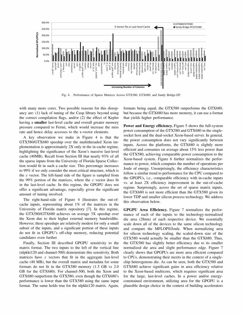
Fig. 4. Performance of Sparse Matrices Across GTX580, GTX680, and Sandy Bridge-EP.
with many more cores. Two possible reasons for this disrep-ancy are: (1) lack of tuning of the Cusp library beyond usingthe correct compilation flags, and/or (2) the effect of Keplerhaving a smaller last-level cache and overall greater memorypressure compared to Fermi, which would increase the missrate and hence delay accesses to the x-vector elements.
A key observation we make in Figure 4 is that theGTX580/GTX680 speedup over the multithreaded Xeon im-plementation is approximately 2X only in the in-cache regime,highlighting the significance of the Xeon’s massive last-levelcache (40MB). Recall from Section III that nearly 93% of allthe sparse inputs from the University of Florida Sparse Collec-tion would fit in such a cache size. This percentage increasesto 99% if we only consider the most critical structure, which isthe x vector. The left-hand side of the figure is sampled fromthe 99% portion of the matrices, where the x vector does fitin the last-level cache. In this regime, the GPGPU does notoffer a significant advantage, especially given the significantamount of tuning involved.
The right-hand-side of Figure 4 illustrates the out-of-cache inputs, representing about 1% of the matrices in theUniversity of Florida matrix repository [7]. In this regime,the GTX580/GTX680 achieves on average 3X speedup overthe Xeon due to their higher external memory bandwidths.However, these speedups are relatively modest for only a smallsubset of the inputs, and a significant portion of these inputsdo not fit in GPGPU’s off-chip memory, reducing potentialcandidates even further.
Finally, Section III described GPGPU sensitivity to thematrix format. The two inputs to the left of the vertical line(nlpkkt120 and channel-500) demonstrate this sensitivity. Bothmatrices have x vectors that fit in the aggregate last-levelcache (40 MB), but the overall matrix and metadata for someformats do not fit in the GTX580 memory (1.5 GB vs 2.0GB for the GTX680). For channel-500, both the Xeon andGTX680 outperform the GTX580, even though the GTX680’sperformance is lower than the GTX580 using the same inputformat. The same holds true for the nlpkkt120 matrix. Again,
formats being equal, the GTX580 outperforms the GTX680,but because the GTX680 has more memory, it can use a formatthat yields higher performance.
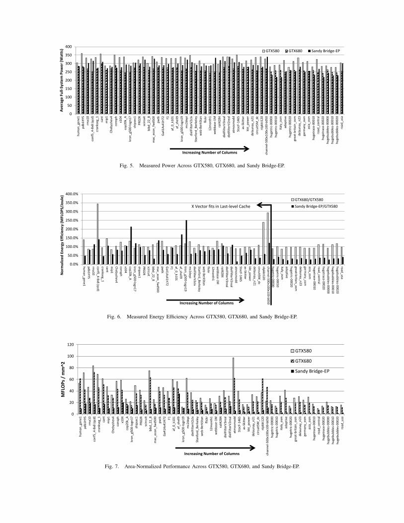
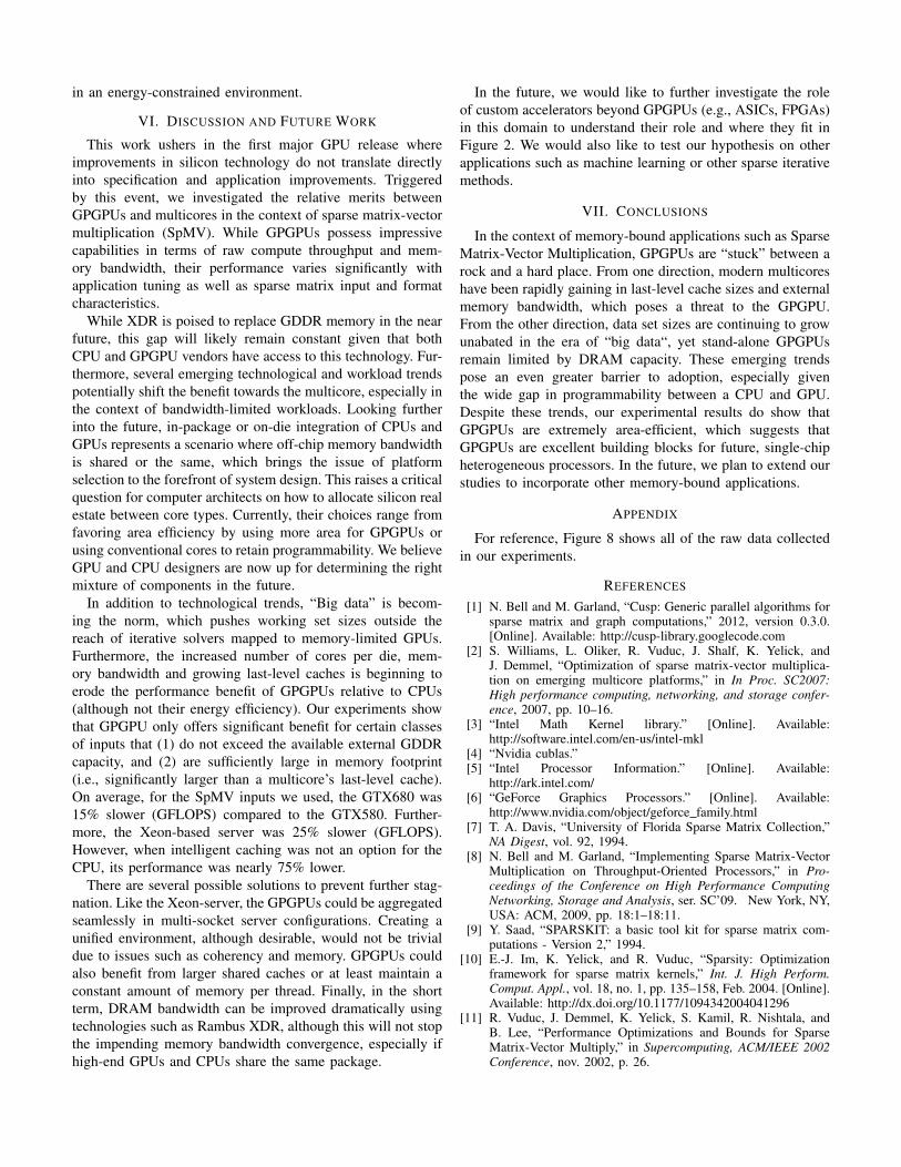
Power and Energy efficiency. Figure 5 shows the full-systempower consumption of the GTX580 and GTX680 in the single-socket host and the dual-socket Xeon-based server. In general,the power consumption does not vary significantly betweeninputs. Across the platforms, the GTX680 is slightly moreefficient and consumes on average about 15% less power thanthe GTX580, achieving comparable power consumption to theXeon-based system. Figure 6 further normalizes the perfor-mance to power, which computes the number of operations perJoule of energy. Unsurprisingly, the efficiency characteristicsfollow a similar trend to performance for the CPU compared tothe GPGPUs, i.e., comparable efficiency with in-cache inputsvs. at least 2X efficiency improvement in the out-of-cacheregime. Surprisingly, across the set of sparse matrix inputs,the GTX680 is not more efficient than the GTX580 given itslower TDP and smaller silicon process technology. We addressthis observation below.
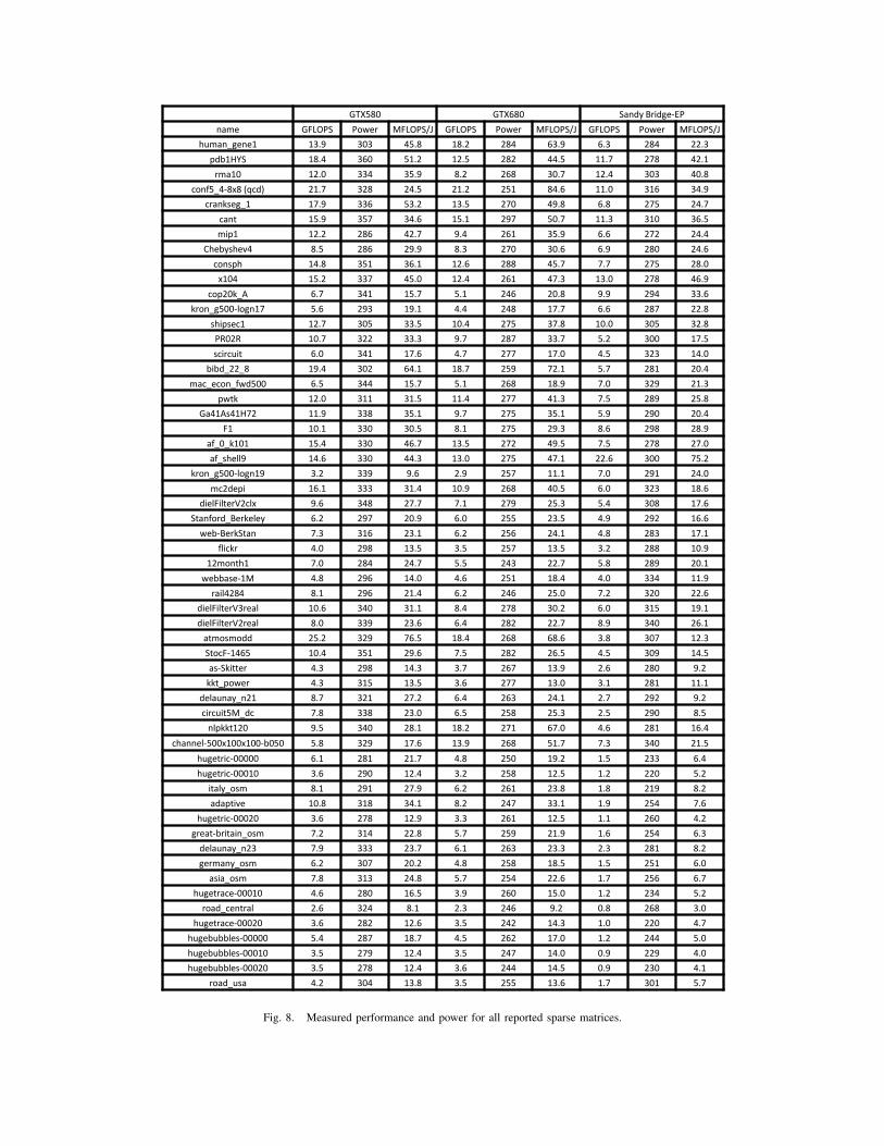
GPGPU Area Efficiency. Figure 7 normalizes the perfor-mance of each of the inputs to the technology-normalizeddie area (28nm) of each respective device. We essentiallyscale down all of the devices to the same silicon technologyand compare the MFLOPS/Joule. When normalizing areafor silicon technology scaling, the scaled-down size of theGTX580 would actually be smaller than the GTX680. Thus,the GTX580 has slightly better efficiency due to its smallernormalized die area and slight performance edge. Figure 7clearly shows that GPGPUs are more area efficient comparedto CPUs, demonstrating their merits in the context of a single-chip heterogenous die. As can be seen, both the GTX580 andGTX680 achieve significant gains in area efficiency relativeto the Xeon-based multicore, which requires significant areafor the large, last-level caches. In a power and/or energy-constrained environment, utilizing area for the GPGPU is aplausible design choice in the context of building accelerators
0
50
100
150
200
250
300
350
400
hu
man
_gen
e1
pd
b1
HYS
rma1
0
con
f5_
4-8
x8 (
qcd
)
cran
kseg
_1
can
t
mip
1
Ch
eb
ysh
ev4
con
sph
x10
4
cop
20
k_A
kro
n_g
50
0-l
ogn
17
ship
sec1
PR
02
R
scir
cuit
bib
d_2
2_
8
mac
_eco
n_
fwd
50
0
pw
tk
Ga4
1A
s41
H7
2 F1
af_0
_k1
01
af_s
he
ll9
kro
n_g
50
0-l
ogn
19
mc2
dep
i
die
lFilt
erV
2cl
x
Stan
ford
_B
erke
ley
we
b-B
erkS
tan
flic
kr
12
mo
nth
1
we
bb
ase-
1M
rail4
28
4
die
lFilt
erV
3re
al
die
lFilt
erV
2re
al
atm
osm
od
d
Sto
cF-1
46
5
as-S
kitt
er
kkt_
po
wer
del
aun
ay_
n2
1
circ
uit
5M
_dc
nlp
kkt1
20
chan
nel
-50
0x1
00
x10
0-b
05
0
hu
getr
ic-0
00
00
hu
getr
ic-0
00
10
ital
y_o
sm
adap
tive
hu
getr
ic-0
00
20
gre
at-b
rita
in_
osm
del
aun
ay_
n2
3
germ
any_
osm
asia
_o
sm
hu
getr
ace-
00
01
0
road
_cen
tral
hu
getr
ace-
00
02
0
hu
geb
ub
ble
s-0
00
00
hu
geb
ub
ble
s-0
00
10
hu
geb
ub
ble
s-0
00
20
road
_usa
Ave
rage
Fu
ll-Sy
ste
m P
ow
er
(Wat
ts)
Increasing Number of Columns
GTX580 GTX680 Sandy Bridge-EP
Fig. 5. Measured Power Across GTX580, GTX680, and Sandy Bridge-EP.
0.0%
50.0%
100.0%
150.0%
200.0%
250.0%
300.0%
350.0%
400.0%
hu
man
_gene
1
pd
b1
HYS
rma1
0
con
f5_
4-8
x8 (q
cd)
crankseg_1
cant
mip
1
Ch
eb
yshe
v4
con
sph
x10
4
cop
20
k_A
kron
_g50
0-lo
gn1
7
ship
sec1
PR
02
R
scircuit
bib
d_2
2_
8
mac_e
con
_fw
d5
00
pw
tk
Ga4
1A
s41
H7
2
F1 af_0_k1
01
af_she
ll9
kron
_g50
0-lo
gn1
9
mc2
dep
i
dielFilterV
2clx
Stanfo
rd_
Berkeley
we
b-B
erkStan
flickr
12
mo
nth
1
we
bb
ase-1M
rail42
84
dielFilterV
3re
al
dielFilterV
2re
al
atmo
smo
dd
StocF-1
46
5
as-Skitter
kkt_po
wer
delau
nay_
n2
1
circuit5
M_d
c
nlp
kkt12
0
chan
nel-5
00
x10
0x1
00
-b0
50
hu
getric-00
00
0
hu
getric-00
01
0
italy_osm
adap
tive
hu
getric-00
02
0
great-b
ritain_
osm
delau
nay_
n2
3
german
y_o
sm
asia_o
sm
hu
getrace-00
01
0
road
_central
hu
getrace-00
02
0
hu
gebu
bb
les-0
00
00
hu
gebu
bb
les-0
00
10
hu
gebu
bb
les-0
00
20
road
_usa
No
rmal
ize
d E
ne
rgy
Effi
cie
ncy
(M
FLO
PS/
Jou
le)
Increasing Number of Columns
GTX680/GTX580
Sandy Bridge-EP/GTX580X Vector fits in Last-level Cache
Fig. 6. Measured Energy Efficiency Across GTX580, GTX680, and Sandy Bridge-EP.
0
20
40
60
80
100
120
hu
man
_gen
e1
pd
b1
HYS
rma1
0
con
f5_
4-8
x8 (
qcd
)
cran
kseg
_1
can
t
mip
1
Ch
eb
ysh
ev4
con
sph
x10
4
cop
20
k_A
kro
n_g
50
0-l
ogn
17
ship
sec1
PR
02
R
scir
cuit
bib
d_2
2_
8
mac
_eco
n_
fwd
50
0
pw
tk
Ga4
1A
s41
H7
2 F1
af_0
_k1
01
af_s
he
ll9
kro
n_g
50
0-l
ogn
19
mc2
dep
i
die
lFilt
erV
2cl
x
Stan
ford
_B
erke
ley
we
b-B
erkS
tan
flic
kr
12
mo
nth
1
we
bb
ase-
1M
rail4
28
4
die
lFilt
erV
3re
al
die
lFilt
erV
2re
al
atm
osm
od
d
Sto
cF-1
46
5
as-S
kitt
er
kkt_
po
wer
del
aun
ay_
n2
1
circ
uit
5M
_dc
nlp
kkt1
20
chan
nel
-50
0x1
00
x10
0-b
05
0
hu
getr
ic-0
00
00
hu
getr
ic-0
00
10
ital
y_o
sm
adap
tive
hu
getr
ic-0
00
20
gre
at-b
rita
in_
osm
del
aun
ay_
n2
3
germ
any_
osm
asia
_o
sm
hu
getr
ace-
00
01
0
road
_cen
tral
hu
getr
ace-
00
02
0
hu
geb
ub
ble
s-0
00
00
hu
geb
ub
ble
s-0
00
10
hu
geb
ub
ble
s-0
00
20
road
_usa
MFL
OP
s /
mm
^2
Increasing Number of Columns
GTX580
GTX680
Sandy Bridge-EP
Fig. 7. Area-Normalized Performance Across GTX580, GTX680, and Sandy Bridge-EP.
in an energy-constrained environment.
VI. DISCUSSION AND FUTURE WORK
This work ushers in the first major GPU release whereimprovements in silicon technology do not translate directlyinto specification and application improvements. Triggeredby this event, we investigated the relative merits betweenGPGPUs and multicores in the context of sparse matrix-vectormultiplication (SpMV). While GPGPUs possess impressivecapabilities in terms of raw compute throughput and mem-ory bandwidth, their performance varies significantly withapplication tuning as well as sparse matrix input and formatcharacteristics.
While XDR is poised to replace GDDR memory in the nearfuture, this gap will likely remain constant given that bothCPU and GPGPU vendors have access to this technology. Fur-thermore, several emerging technological and workload trendspotentially shift the benefit towards the multicore, especially inthe context of bandwidth-limited workloads. Looking furtherinto the future, in-package or on-die integration of CPUs andGPUs represents a scenario where off-chip memory bandwidthis shared or the same, which brings the issue of platformselection to the forefront of system design. This raises a criticalquestion for computer architects on how to allocate silicon realestate between core types. Currently, their choices range fromfavoring area efficiency by using more area for GPGPUs orusing conventional cores to retain programmability. We believeGPU and CPU designers are now up for determining the rightmixture of components in the future.
In addition to technological trends, “Big data” is becom-ing the norm, which pushes working set sizes outside thereach of iterative solvers mapped to memory-limited GPUs.Furthermore, the increased number of cores per die, mem-ory bandwidth and growing last-level caches is beginning toerode the performance benefit of GPGPUs relative to CPUs(although not their energy efficiency). Our experiments showthat GPGPU only offers significant benefit for certain classesof inputs that (1) do not exceed the available external GDDRcapacity, and (2) are sufficiently large in memory footprint(i.e., significantly larger than a multicore’s last-level cache).On average, for the SpMV inputs we used, the GTX680 was15% slower (GFLOPS) compared to the GTX580. Further-more, the Xeon-based server was 25% slower (GFLOPS).However, when intelligent caching was not an option for theCPU, its performance was nearly 75% lower.
There are several possible solutions to prevent further stag-nation. Like the Xeon-server, the GPGPUs could be aggregatedseamlessly in multi-socket server configurations. Creating aunified environment, although desirable, would not be trivialdue to issues such as coherency and memory. GPGPUs couldalso benefit from larger shared caches or at least maintain aconstant amount of memory per thread. Finally, in the shortterm, DRAM bandwidth can be improved dramatically usingtechnologies such as Rambus XDR, although this will not stopthe impending memory bandwidth convergence, especially ifhigh-end GPUs and CPUs share the same package.
In the future, we would like to further investigate the roleof custom accelerators beyond GPGPUs (e.g., ASICs, FPGAs)in this domain to understand their role and where they fit inFigure 2. We would also like to test our hypothesis on otherapplications such as machine learning or other sparse iterativemethods.
VII. CONCLUSIONS
In the context of memory-bound applications such as SparseMatrix-Vector Multiplication, GPGPUs are “stuck” between arock and a hard place. From one direction, modern multicoreshave been rapidly gaining in last-level cache sizes and externalmemory bandwidth, which poses a threat to the GPGPU.From the other direction, data set sizes are continuing to growunabated in the era of “big data“, yet stand-alone GPGPUsremain limited by DRAM capacity. These emerging trendspose an even greater barrier to adoption, especially giventhe wide gap in programmability between a CPU and GPU.Despite these trends, our experimental results do show thatGPGPUs are extremely area-efficient, which suggests thatGPGPUs are excellent building blocks for future, single-chipheterogeneous processors. In the future, we plan to extend ourstudies to incorporate other memory-bound applications.
APPENDIX
For reference, Figure 8 shows all of the raw data collectedin our experiments.
REFERENCES
[1] N. Bell and M. Garland, “Cusp: Generic parallel algorithms forsparse matrix and graph computations,” 2012, version 0.3.0.[Online]. Available: http://cusp-library.googlecode.com
[2] S. Williams, L. Oliker, R. Vuduc, J. Shalf, K. Yelick, andJ. Demmel, “Optimization of sparse matrix-vector multiplica-tion on emerging multicore platforms,” in In Proc. SC2007:High performance computing, networking, and storage confer-ence, 2007, pp. 10–16.
[3] “Intel Math Kernel library.” [Online]. Available:http://software.intel.com/en-us/intel-mkl
[4] “Nvidia cublas.”[5] “Intel Processor Information.” [Online]. Available:
http://ark.intel.com/[6] “GeForce Graphics Processors.” [Online]. Available:
http://www.nvidia.com/object/geforce family.html[7] T. A. Davis, “University of Florida Sparse Matrix Collection,”
NA Digest, vol. 92, 1994.[8] N. Bell and M. Garland, “Implementing Sparse Matrix-Vector
Multiplication on Throughput-Oriented Processors,” in Pro-ceedings of the Conference on High Performance ComputingNetworking, Storage and Analysis, ser. SC’09. New York, NY,USA: ACM, 2009, pp. 18:1–18:11.
[9] Y. Saad, “SPARSKIT: a basic tool kit for sparse matrix com-putations - Version 2,” 1994.
[10] E.-J. Im, K. Yelick, and R. Vuduc, “Sparsity: Optimizationframework for sparse matrix kernels,” Int. J. High Perform.Comput. Appl., vol. 18, no. 1, pp. 135–158, Feb. 2004. [Online].Available: http://dx.doi.org/10.1177/1094342004041296
[11] R. Vuduc, J. Demmel, K. Yelick, S. Kamil, R. Nishtala, andB. Lee, “Performance Optimizations and Bounds for SparseMatrix-Vector Multiply,” in Supercomputing, ACM/IEEE 2002Conference, nov. 2002, p. 26.
GTX580 GTX680 Sandy Bridge-EP
name GFLOPS Power MFLOPS/J GFLOPS Power MFLOPS/J GFLOPS Power MFLOPS/J
human_gene1 13.9 303 45.8 18.2 284 63.9 6.3 284 22.3
pdb1HYS 18.4 360 51.2 12.5 282 44.5 11.7 278 42.1
rma10 12.0 334 35.9 8.2 268 30.7 12.4 303 40.8
conf5_4-8x8 (qcd) 21.7 328 24.5 21.2 251 84.6 11.0 316 34.9
crankseg_1 17.9 336 53.2 13.5 270 49.8 6.8 275 24.7
cant 15.9 357 34.6 15.1 297 50.7 11.3 310 36.5
mip1 12.2 286 42.7 9.4 261 35.9 6.6 272 24.4
Chebyshev4 8.5 286 29.9 8.3 270 30.6 6.9 280 24.6
consph 14.8 351 36.1 12.6 288 45.7 7.7 275 28.0
x104 15.2 337 45.0 12.4 261 47.3 13.0 278 46.9
cop20k_A 6.7 341 15.7 5.1 246 20.8 9.9 294 33.6
kron_g500-logn17 5.6 293 19.1 4.4 248 17.7 6.6 287 22.8
shipsec1 12.7 305 33.5 10.4 275 37.8 10.0 305 32.8
PR02R 10.7 322 33.3 9.7 287 33.7 5.2 300 17.5
scircuit 6.0 341 17.6 4.7 277 17.0 4.5 323 14.0
bibd_22_8 19.4 302 64.1 18.7 259 72.1 5.7 281 20.4
mac_econ_fwd500 6.5 344 15.7 5.1 268 18.9 7.0 329 21.3
pwtk 12.0 311 31.5 11.4 277 41.3 7.5 289 25.8
Ga41As41H72 11.9 338 35.1 9.7 275 35.1 5.9 290 20.4
F1 10.1 330 30.5 8.1 275 29.3 8.6 298 28.9
af_0_k101 15.4 330 46.7 13.5 272 49.5 7.5 278 27.0
af_shell9 14.6 330 44.3 13.0 275 47.1 22.6 300 75.2
kron_g500-logn19 3.2 339 9.6 2.9 257 11.1 7.0 291 24.0
mc2depi 16.1 333 31.4 10.9 268 40.5 6.0 323 18.6
dielFilterV2clx 9.6 348 27.7 7.1 279 25.3 5.4 308 17.6
Stanford_Berkeley 6.2 297 20.9 6.0 255 23.5 4.9 292 16.6
web-BerkStan 7.3 316 23.1 6.2 256 24.1 4.8 283 17.1
flickr 4.0 298 13.5 3.5 257 13.5 3.2 288 10.9
12month1 7.0 284 24.7 5.5 243 22.7 5.8 289 20.1
webbase-1M 4.8 296 14.0 4.6 251 18.4 4.0 334 11.9
rail4284 8.1 296 21.4 6.2 246 25.0 7.2 320 22.6
dielFilterV3real 10.6 340 31.1 8.4 278 30.2 6.0 315 19.1
dielFilterV2real 8.0 339 23.6 6.4 282 22.7 8.9 340 26.1
atmosmodd 25.2 329 76.5 18.4 268 68.6 3.8 307 12.3
StocF-1465 10.4 351 29.6 7.5 282 26.5 4.5 309 14.5
as-Skitter 4.3 298 14.3 3.7 267 13.9 2.6 280 9.2
kkt_power 4.3 315 13.5 3.6 277 13.0 3.1 281 11.1
delaunay_n21 8.7 321 27.2 6.4 263 24.1 2.7 292 9.2
circuit5M_dc 7.8 338 23.0 6.5 258 25.3 2.5 290 8.5
nlpkkt120 9.5 340 28.1 18.2 271 67.0 4.6 281 16.4
channel-500x100x100-b050 5.8 329 17.6 13.9 268 51.7 7.3 340 21.5
hugetric-00000 6.1 281 21.7 4.8 250 19.2 1.5 233 6.4
hugetric-00010 3.6 290 12.4 3.2 258 12.5 1.2 220 5.2
italy_osm 8.1 291 27.9 6.2 261 23.8 1.8 219 8.2
adaptive 10.8 318 34.1 8.2 247 33.1 1.9 254 7.6
hugetric-00020 3.6 278 12.9 3.3 261 12.5 1.1 260 4.2
great-britain_osm 7.2 314 22.8 5.7 259 21.9 1.6 254 6.3
delaunay_n23 7.9 333 23.7 6.1 263 23.3 2.3 281 8.2
germany_osm 6.2 307 20.2 4.8 258 18.5 1.5 251 6.0
asia_osm 7.8 313 24.8 5.7 254 22.6 1.7 256 6.7
hugetrace-00010 4.6 280 16.5 3.9 260 15.0 1.2 234 5.2
road_central 2.6 324 8.1 2.3 246 9.2 0.8 268 3.0
hugetrace-00020 3.6 282 12.6 3.5 242 14.3 1.0 220 4.7
hugebubbles-00000 5.4 287 18.7 4.5 262 17.0 1.2 244 5.0
hugebubbles-00010 3.5 279 12.4 3.5 247 14.0 0.9 229 4.0
hugebubbles-00020 3.5 278 12.4 3.6 244 14.5 0.9 230 4.1
road_usa 4.2 304 13.8 3.5 255 13.6 1.7 301 5.7
Fig. 8. Measured performance and power for all reported sparse matrices.

[12] A. Buluc, J. T. Fineman, M. Frigo, J. R. Gilbert, and C. E.Leiserson, “Parallel sparse matrix-vector and matrix-transpose-vector multiplication using compressed sparse blocks,” in Pro-ceedings of the twenty-first annual symposium on Parallelism inalgorithms and architectures, ser. SPAA’09. New York, NY,USA: ACM, 2009, pp. 233–244.
[13] A. Buluc, S. Williams, L. Oliker, and J. Demmel, “Reduced-Bandwidth Multithreaded Algorithms for Sparse Matrix-VectorMultiplication,” in Proceedings of the 2011 IEEE InternationalParallel & Distributed Processing Symposium, ser. IPDPS’11.Washington, DC, USA: IEEE Computer Society, 2011, pp. 721–733.
[14] V. W. Lee, C. Kim, J. Chhugani, M. Deisher, D. Kim,A. D. Nguyen, N. Satish, M. Smelyanskiy, S. Chennupaty,P. Hammarlund, R. Singhal, and P. Dubey, “Debunkingthe 100x gpu vs. cpu myth: an evaluation of throughputcomputing on cpu and gpu,” in Proceedings of the 37th annualinternational symposium on Computer architecture, ser. ISCA’10. New York, NY, USA: ACM, 2010, pp. 451–460. [Online].Available: http://doi.acm.org/10.1145/1815961.1816021
[15] “Joulemeter: Computational Energy Measure-ment and Optimization.” [Online]. Available:http://research.microsoft.com/en-us/projects/joulemeter/
[16] I. Park and R. Buch, “Improve debugging andperformance tuning with etw,” 2007. [Online]. Available:http://msdn.microsoft.com/en-us/magazine/cc163437.aspx