spontaneous high piezoelectricity in article poly ...4unano.com/bg/papers/bayindir group -...
TRANSCRIPT

KANIK ET AL. VOL. 8 ’ NO. 9 ’ 9311–9323 ’ 2014
www.acsnano.org
9311
August 18, 2014
C 2014 American Chemical Society
Spontaneous High Piezoelectricity inPoly(vinylidene fluoride) NanoribbonsProduced by Iterative Thermal SizeReduction TechniqueMehmet Kanik,†,‡ Ozan Aktas,†,§ Huseyin Sener Sen,† Engin Durgun,†,‡ and Mehmet Bayindir†,‡,§,*
†UNAM-National Nanotechnology Research Center, Bilkent University, 06800 Ankara, Turkey, ‡Institute of Materials Science and Nanotechnology, Bilkent University,06800 Ankara, Turkey, and §Department of Physics, Bilkent University, 06800 Ankara, Turkey
Utilization of the unique materialproperties represented by flexi-ble, lightweight and biocompatible
piezoelectric polymeric materials such aspoly(vinylidene fluoride) (PVDF)1 and itscopolymer poly(vinylidene fluoride trifluoro-ethylene) (PVDF-TrFE)2 is expected to bringon new horizons for sensor, actuator, andenergy harvesting applications where piezo-electric ceramic materials have been em-ployed hitherto. A closer look into theapplications of piezoelectricity includingbiosensing,3 energy generation,4�6 pressuresensing,7 high precision positioning,8 artifi-cialmuscle and skin9,10 reveals that thermallystable, flexible, and stretchable piezoelectricmaterials are required to be produced withhigh yields and in a cost-effective way forthe fabrication of commercially feasible, largearea, self-powering, and highly efficient de-vices. Although ceramic piezoelectricmaterials
can present higher piezoelectric coefficients,they suffer from high brittleness, low cyclicendurance, high processing temperatureand high production cost as well as toxicelemental composition in contrast to proper-ties of polymer piezoelectric materials.11,12
Since the discovery of PVDF (CH2�CF2)n,which has the highest piezoelectric coeffi-cient among all polymers,1 PVDF and copo-lymers have been a subject of intenseresearch, which initiated development ofmany fabrication methods for PVDF thinfilm13 and nanowires.14 Regardless of theproduction method, piezoelectric proper-ties are dependent on the amount of polarphase of PVDF.15,16 Four commonly knownforms of PVDF are R, β, γ and δ phases,which are represented by different stereo-chemical structures with alternating s-transand s-gauge C�C bonds (TGTG, TTTT,TTTGTTTG, and TGTG(polar)), respectively.
15,17
* Address correspondence [email protected].
Received for review June 16, 2014and accepted August 18, 2014.
Published online10.1021/nn503269b
ABSTRACT We produced kilometer-long, endlessly parallel, spontaneously
piezoelectric and thermally stable poly(vinylidene fluoride) (PVDF) micro- and
nanoribbons using iterative size reduction technique based on thermal fiber
drawing. Because of high stress and temperature used in thermal drawing
process, we obtained spontaneously polar γ phase PVDF micro- and nanoribbons
without electrical poling process. On the basis of X-ray diffraction (XRD) analysis,
we observed that PVDF micro- and nanoribbons are thermally stable and conserve
the polar γ phase even after being exposed to heat treatment above the melting
point of PVDF. Phase transition mechanism is investigated and explained using
ab initio calculations. We measured an average effective piezoelectric constant as �58.5 pm/V from a single PVDF nanoribbon using a piezo evaluation
system along with an atomic force microscope. PVDF nanoribbons are promising structures for constructing devices such as highly efficient energy
generators, large area pressure sensors, artificial muscle and skin, due to the unique geometry and extended lengths, high polar phase content, high
thermal stability and high piezoelectric coefficient. We demonstrated two proof of principle devices for energy harvesting and sensing applications with a
60 V open circuit peak voltage and 10 μA peak short-circuit current output.
KEYWORDS: piezoelectric polymer . nanoribbon . fiber drawing . PVDF . energy harvesting . ab initio calculation
ARTIC
LE
KANIK ET AL. VOL. 8 ’ NO. 9 ’ 9311–9323 ’ 2014
www.acsnano.org
9312
Themost stable and easily obtained formof PVDF is thenonpolar R phase, which can also be in a rarely foundpolar form named δ phase. On the other hand, β and γphases are the most desirable forms of PVDF due totheir high polar molecular conformations.14,18�21 Highpolarity of theβ phase as a result of all trans C�Cbondsmakes PVDF a promising candidate for piezoelectric,pyroelectric and ferroelectric applications.7,14,18,19
Transitions betweenphases of PVDF are possible underspecific nucleation and processing conditions (Figure S1,Supporting Information (SI)). Irrespective of the initialphase, the amount of the β phase in PVDF thin filmscan be increased by adding inorganic additives orstretching more than 80% at 95 �C following with anelectrical poling.15,22 Transition mechanisms resultingin γ phase are crystallization at high temperature orapplying high shear on molten polymer, long-termannealing at high temperature or polling at low electricfield from R phase, and low rate evaporation from hightemperature polymer solutions.16,20,21,23 Although, γphase has lower polarity when compared to β phase,its piezoelectric coefficient still stands better thanthose of other polymers.17,20 Besides, the higher Curietemperature of γ phase makes it less vulnerable toharsh environmental conditions. Because of the decayof remnant polarization of β phase PVDF and PVDF-TrFEat lower Curie temperatures, these materials are notgood candidates for production of thermally stable longendurance devices.24 Because of its superior properties,γ phase is highly desirable. Unfortunately, it is known tobe hard to access experimentally.20
The most common way of triggering polar phasetransitions is applying a high strength electric field atelevated temperatures.14,25,26 In addition, diminishingthe feature size of PVDF lowers the cost and energyrequired for the polarization process.27 In accordancewith the developments in nanotechnology, scientistshave been trying to facilitate nanoscale effects toimprove the piezoelectric properties of PVDF andcopolymers by altering their composition,21,22,28,29 sizeand shape.18�20,23,27,30,31 Initial attempts were focusedon developing PVDF piezoelectric thin films by usingspray coating,32 spin coating,17 physical vapor deposi-tion,33 and the Langmuir�Blodgett thin film coatingmethods.34 Although shaping the PVDF in the form ofthin film can disclose elevated piezoelectric properties,PVDF nanowires lead to superior piezoelectricity, due tothe one-dimensional nanoscale confinement.7,14 Resultsof nanoconfinement effects such as spontaneous polar-ization can eliminate external electrical poling process forpolar phase transition.19,20,31
Beyond the controversy, nanowires have madegreat impacts onmany disciplines including solar cells,biosensors and phase change memory devices.35�38
A similar impact is also expected on piezoelectricapplications using PVDF nanowires. The prominentpiezoelectric PVDF nanowire fabrication methods are
anodized alumina (AAO) template molding,19,20,39
electrospinning,7,14,40,41 and nanoimprint lithography(NI),18,23,27,31 which are all solvent dependent. Eventhough these techniques are appropriate to producePVDF nanowires, they are not superior in all aspectsconsidering the nanowire aspect ratio, uniformity,geometry control, yield, and device integrability inorder to produce large area, low cost and highthroughput devices (Table S1 (SI)). Despite the factthat high aspect ratio nanowires can be produced withhigh yield by using electrospinning, diameter unifor-mity and geometry control capability of this techniqueare not fulfilling the requirements of current state ofthe art technology. Tuning the diameter of nanowirescan be better accomplished by using AAO and NItechniques. However, nanowires produced by thesemethods are not feasible to carry out the production offlexible, large area devices. Above all, unlike electro-spinning, AAO, and NI techniques, a fabrication tech-nique that provides PVDF nanowire production withhigh aspect ratio, excellent uniformity, desired geome-try, and high yield in a multimaterial fashion can pavethe way for in situ assembly of nanowires withmetallic,semiconductor and dielectric components of themacroscopic devices.42,43
RESULTS AND DISCUSSION
Compatibility of iterative fiber drawing based sizereduction technique for a wide range of materials innanowire shape has been demonstrated.43�45 On thecontrary to a recent study,46 it is possible to producemicro- and nanostructured PVDF in polar phase spon-taneously induced by fiber drawing process as weshowed in this study for the first time. Here, weproduced kilometer-long, PVDF arrays in novel formssuch as nanoribbon and square cross-sectional nano-shell (Figure S2 (SI)) structures. We rather prefer ribbonshape with planar contact areas, which poses a uniqueadvantage for piezoelectric measurements, unlike thenanowires with cylindrical symmetry. We achievedhighly polar γ phase PVDF nanoribbons from the fiberdrawing technique simultaneously utilizing high tem-perature and shear stress triggered by tensile forces(Figure S3 and Video S1 (SI)). In order to simulate thephase transformation in iterative fiber drawing pro-cess, we performed ab initio calculations based ondensity functional theory in which the effects of bothtemperature and shear stress are included. The detailsof the method are explained in the Supporting Infor-mation. We compared the phase transition at 0 and470 K (above the melting temperature of PVDF) from Rand β phase to γ phase under varying compressive andtensile strain. γ phase in the as produced PVDF nano-ribbons is observed to still exist after annealing at hightemperatures up to 175 �C. R, β and γ phase distribu-tion in PVDF ribbons are investigated as a function ofsize using X-ray diffraction (XRD) and attenuated total
ARTIC
LE

KANIK ET AL. VOL. 8 ’ NO. 9 ’ 9311–9323 ’ 2014
www.acsnano.org
9313
reflectance�fourier transform infrared (ATR�FTIR)spectroscopy techniques. PVDF ribbons are confirmedby morphological characterizations conducted withscanning electron microscopy (SEM). Using a piezoevaluation system attached to an atomic force micro-scope (AFM), we observed a large piezoelectric re-sponse (d33= �58.5 pm/V) from a single 80 nm thicknanoribbon. To our knowledge, this is the first piezo-electric measurement performed on a single PVDFnanoribbon. Besides, here we report the highest effec-tive d33 coefficient ever measured from a γ phasesingle PVDF nanoribbon. To utilize the superior perfor-mance, we designed two different device structures forthe purpose of energy harvesting and tapping sensor.Peak voltage and current outputs of our devices aremeasured as 60 V and 10 μA.The nanoribbon fabrication procedure starts with
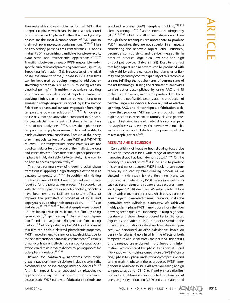
preparation of a multimaterial preform, which is anexact macroscopic copy of the final fibers. The easiestway to produce a preform is rolling polymer films,degassing the air trapped in the roll under a vacuum ata temperature below the glass transition temperatureof the films and last consolidating in a vacuum oven atthe glass transition temperature of the films. Followingthe mentioned procedure, a PVDF preform is preparedby rolling 60 μm thick PVDF films around a glass tubeand consolidated in a tube oven at 180 �C for 30 minunder a 2 � 10�2 Torr vacuum. Next, a slab (3 mm �10 mm � 10 cm) is mechanically extracted from thisPVDF preform. Afterward, a poly(ether sulfone) (PES)preformwith 35mm in diameter and 25 cm in length ismade by rolling 100 μm thick PES films around a 3 mmglass tube and consolidated at 255 �C for 35min undera 2� 10�2 Torr vacuum. The PES preform is split in twohalves and machined in the center to open a niche forinserting the PVDF slab (Figure 1a).Fiber drawing processes are executed in a custom-
made fiber tower, which consists of a vertical tubeoven, a preform feeding mechanism, and a real timemonitoring systemmeasuring applied stress, tempera-ture, and thickness of the drawn fiber (Figure S4 (SI)).Figure 1b summarizes the nanoribbon fabricationtechnique. The fabrication of PVDF nanoribbon arrays,which comprises several fiber drawing steps, startswith the drawing of PVDF slab embedded PES preform.Heating the preform above the glass transition tem-perature of PES and melting point of PVDF and apply-ing approximately 3 MPa tensile stress are required inorder to trigger plastic deformation in fiber drawingprocess. Since drawing temperature (285 �C) or thetemperature in the core of the preform (∼200 �C) ishigher than the melting point of PVDF (Tm = 165 �C),the molten slab flows and shrinks in the PES claddingduring fiber drawing. The first step of thermal drawingprocess results in PVDF microribbons with variousthicknesses ranging from 400 to 10 μm by adjustingthe process temperature, applied stress, drawing and
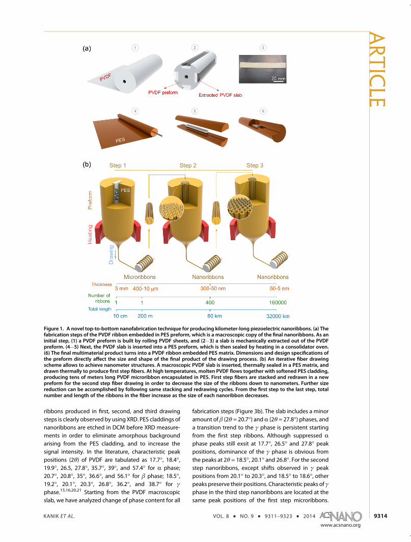
feeding speed. Figure 2a shows as drawn step 1 fibersand Figure 2b represents cross sectional and long-itudinal SEM images of 30 μm thick microribbonembedded fibers, which are produced in the first stepwith a preform feeding speed 8 mm/sec. For thesecond drawing step, approximately 400 first stepfibers are stacked and inserted into cylindrical hollowcore of a new PES preform, which becomes a multi-functional jacket protecting and keeping the PVDFnanoribbons together. Sequential thermal drawingsof the preform prepared for the second step result inthicknesses ranging from 300 to 50 nm (Figure 2c,d).Similarly, 400 nanoribbon embedded fibers obtainedin previous steps are inserted in new PES preformsproduced for the third step fiber drawing processes.After drawing the third step preform, nanoribbonsresult in thicknesses ranging from 50 to 5 nm(Figure 2e,f). We extracted PVDF nanoribbons out ofthe PES cladding by using dichloromethane (DCM),which cannot dissolve PVDF. Cross sectional character-ization of nanoribbons requires a special sample pre-paration using ultramicrotome for SEM imaging.However, diamond knife of the ultramicrotome causesdefects that hamper observing the exact cross sec-tional shape of the nanoribbons. In addition, eventhough state of the art electronmicroscopy techniquesare used, imaging of nanometer scale polymer featuresis very difficult due to fast degradation of polymersunder high energy electron beam.47 Alternatively,a better SEM observation of the ribbon shape isaccomplished using two different sample preparationmethods: breaking the fibers after a liquid nitrogentreatment (Figure S5 (SI)) and direct cutting of thefibers longitudinally (Video S2 (SI)). Size distribution forsecond step PVDF nanoribbons is given in Figure S6 (SI).Standard deviation normalized with respect to themean of the nanoribbons size distribution is found tobe ∼11%.The distance between nanoribbons is well-defined
with cladding thicknesses of the input fibers. In addi-tion, the macroscopic encapsulation polymer makes itpracticable to manually manipulate kilometers long,perfectly aligned, millions of nanowires. Number andtotal lengths of the nanoribbon embedded fibers areprogressive in conformity with the growing number ofdrawing steps. For instance, despite that a 200 m longin-fiber single ribbon is obtained after the first stepdrawing, nanoribbons are achieved in kilometers oflength and thousands of number in following drawingsteps. Dimensions of the first step slab and preform,overall reduction ratio, and the number of steps initerative fiber drawing processes determine the finalsize of nanoribbons. Besides, ribbon shape is inheritedby next generation ribbons from the fibers produced inprevious steps.Molecular conformation of R, β and γ phases are
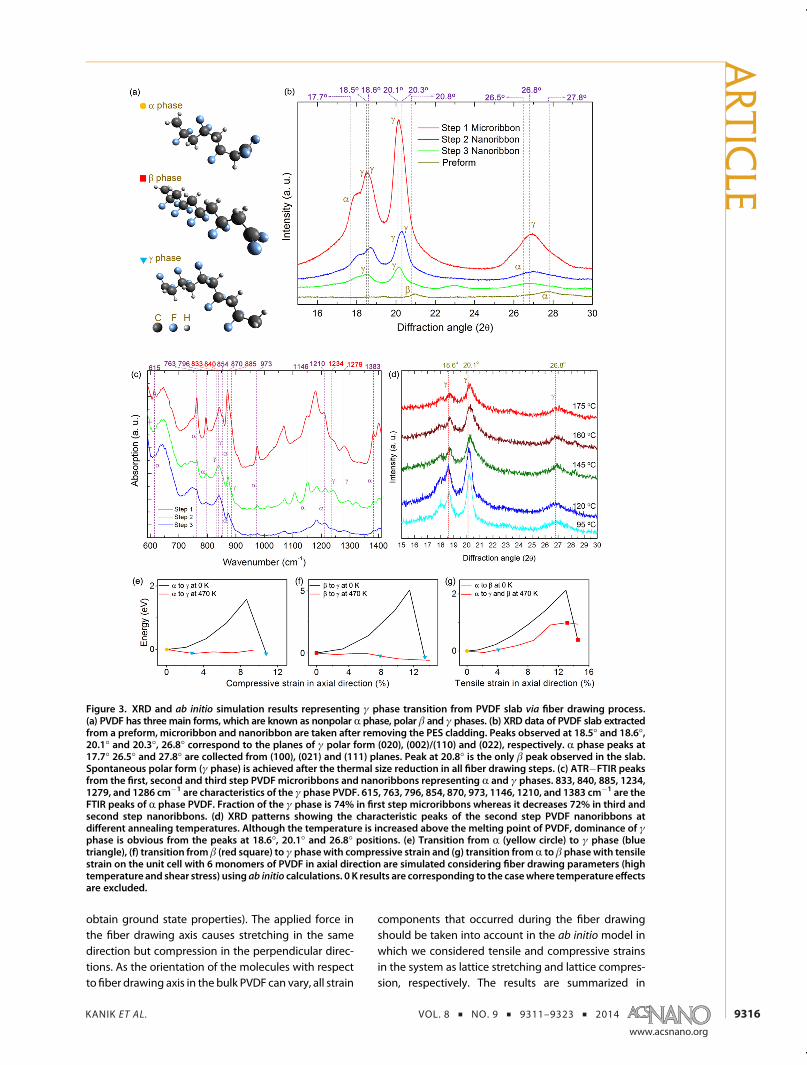
shown in Figure 3a. Predominance of the polar γ phase
ARTIC
LE
KANIK ET AL. VOL. 8 ’ NO. 9 ’ 9311–9323 ’ 2014
www.acsnano.org
9314
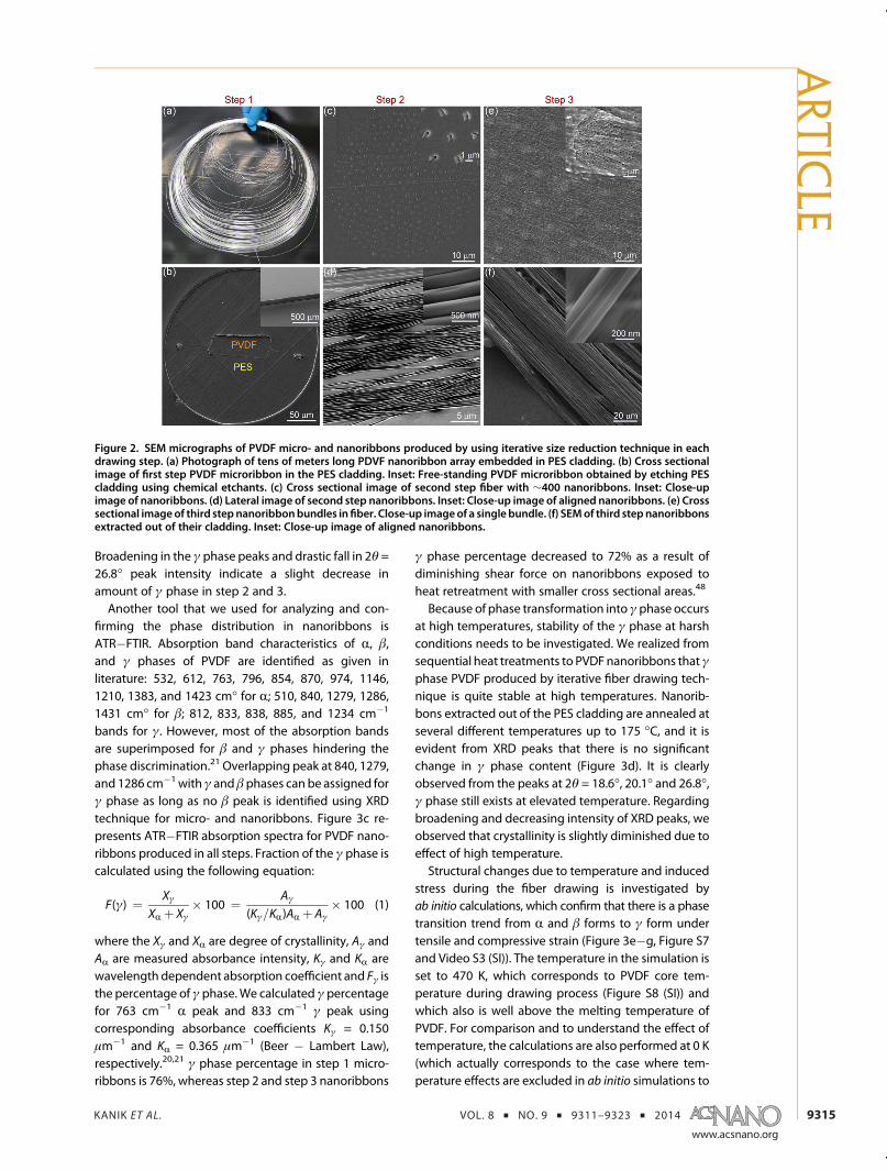
ribbons produced in first, second, and third drawingsteps is clearly observed by using XRD. PES claddings ofnanoribbons are etched in DCM before XRD measure-ments in order to eliminate amorphous backgroundarising from the PES cladding, and to increase thesignal intensity. In the literature, characteristic peakpositions (2θ) of PVDF are tabulated as 17.7�, 18.4�,19.9�, 26.5, 27.8�, 35.7�, 39�, and 57.4� for R phase;20.7�, 20.8�, 35�, 36.6�, and 56.1� for β phase; 18.5�,19.2�, 20.1�, 20.3�, 26.8�, 36.2�, and 38.7� for γphase.15,16,20,21 Starting from the PVDF macroscopicslab, we have analyzed change of phase content for all
fabrication steps (Figure 3b). The slab includes a minoramount of β (2θ = 20.7�) andR (2θ = 27.8�) phases, anda transition trend to the γ phase is persistent startingfrom the first step ribbons. Although suppressed Rphase peaks still exsit at 17.7�, 26.5� and 27.8� peakpositions, dominance of the γ phase is obvious fromthe peaks at 2θ = 18.5�, 20.1� and 26.8�. For the secondstep nanoribbons, except shifts observed in γ peakpositions from 20.1� to 20.3�, and 18.5� to 18.6�, otherpeaks preserve their positions. Characteristic peaks of γphase in the third step nanoribbons are located at thesame peak positions of the first step microribbons.
Figure 1. A novel top-to-bottom nanofabrication technique for producing kilometer-long piezoelectric nanoribbons. (a) Thefabrication steps of the PVDF ribbon embedded in PES preform, which is a macroscopic copy of the final nanoribbons. As aninitial step, (1) a PVDF preform is built by rolling PVDF sheets, and (2�3) a slab is mechanically extracted out of the PVDFpreform. (4�5) Next, the PVDF slab is inserted into a PES preform, which is then sealed by heating in a consolidator oven.(6) The final multimaterial product turns into a PVDF ribbon embedded PES matrix. Dimensions and design specifications ofthe preform directly affect the size and shape of the final product of the drawing process. (b) An iterative fiber drawingscheme allows to achieve nanometer structures. A macroscopic PVDF slab is inserted, thermally sealed in a PES matrix, anddrawn thermally to produce first step fibers. At high temperatures, molten PVDF flows together with softened PES cladding,producing tens of meters long PVDF microribbon encapsulated in PES. First step fibers are stacked and redrawn in a newpreform for the second step fiber drawing in order to decrease the size of the ribbons down to nanometers. Further sizereduction can be accomplished by following same stacking and redrawing cycles. From the first step to the last step, totalnumber and length of the ribbons in the fiber increase as the size of each nanoribbon decreases.
ARTIC
LE
KANIK ET AL. VOL. 8 ’ NO. 9 ’ 9311–9323 ’ 2014
www.acsnano.org
9315
Broadening in the γ phase peaks and drastic fall in 2θ =26.8� peak intensity indicate a slight decrease inamount of γ phase in step 2 and 3.Another tool that we used for analyzing and con-
firming the phase distribution in nanoribbons isATR�FTIR. Absorption band characteristics of R, β,and γ phases of PVDF are identified as given inliterature: 532, 612, 763, 796, 854, 870, 974, 1146,1210, 1383, and 1423 cm� for R; 510, 840, 1279, 1286,1431 cm� for β; 812, 833, 838, 885, and 1234 cm�1
bands for γ. However, most of the absorption bandsare superimposed for β and γ phases hindering thephase discrimination.21 Overlapping peak at 840, 1279,and 1286 cm�1with γ andβphases can be assigned forγ phase as long as no β peak is identified using XRDtechnique for micro- and nanoribbons. Figure 3c re-presents ATR�FTIR absorption spectra for PVDF nano-ribbons produced in all steps. Fraction of the γ phase iscalculated using the following equation:
F(γ) ¼ XγXR þ Xγ
� 100 ¼ Aγ
(Kγ=KR)AR þAγ� 100 (1)
where the Xγ and XR are degree of crystallinity, Aγ andAR are measured absorbance intensity, Kγ and KR arewavelength dependent absorption coefficient and Fγ isthe percentage of γ phase.We calculated γ percentagefor 763 cm�1 R peak and 833 cm�1 γ peak usingcorresponding absorbance coefficients Kγ = 0.150μm�1 and KR = 0.365 μm�1 (Beer � Lambert Law),respectively.20,21 γ phase percentage in step 1 micro-ribbons is 76%, whereas step 2 and step 3 nanoribbons
γ phase percentage decreased to 72% as a result ofdiminishing shear force on nanoribbons exposed toheat retreatment with smaller cross sectional areas.48
Because of phase transformation into γphase occursat high temperatures, stability of the γ phase at harshconditions needs to be investigated. We realized fromsequential heat treatments to PVDFnanoribbons thatγphase PVDF produced by iterative fiber drawing tech-nique is quite stable at high temperatures. Nanorib-bons extracted out of the PES cladding are annealed atseveral different temperatures up to 175 �C, and it isevident from XRD peaks that there is no significantchange in γ phase content (Figure 3d). It is clearlyobserved from the peaks at 2θ = 18.6�, 20.1� and 26.8�,γ phase still exists at elevated temperature. Regardingbroadening and decreasing intensity of XRD peaks, weobserved that crystallinity is slightly diminished due toeffect of high temperature.Structural changes due to temperature and induced
stress during the fiber drawing is investigated byab initio calculations, which confirm that there is a phasetransition trend from R and β forms to γ form undertensile and compressive strain (Figure 3e�g, Figure S7and Video S3 (SI)). The temperature in the simulation isset to 470 K, which corresponds to PVDF core tem-perature during drawing process (Figure S8 (SI)) andwhich also is well above the melting temperature ofPVDF. For comparison and to understand the effect oftemperature, the calculations are also performed at 0 K(which actually corresponds to the case where tem-perature effects are excluded in ab initio simulations to
Figure 2. SEM micrographs of PVDF micro- and nanoribbons produced by using iterative size reduction technique in eachdrawing step. (a) Photograph of tens of meters long PDVF nanoribbon array embedded in PES cladding. (b) Cross sectionalimage of first step PVDF microribbon in the PES cladding. Inset: Free-standing PVDF microribbon obtained by etching PEScladding using chemical etchants. (c) Cross sectional image of second step fiber with ∼400 nanoribbons. Inset: Close-upimage of nanoribbons. (d) Lateral image of second step nanoribbons. Inset: Close-up image of aligned nanoribbons. (e) Crosssectional imageof third stepnanoribbonbundles infiber. Close-up imageof a single bundle. (f) SEMof third stepnanoribbonsextracted out of their cladding. Inset: Close-up image of aligned nanoribbons.
ARTIC
LE
KANIK ET AL. VOL. 8 ’ NO. 9 ’ 9311–9323 ’ 2014
www.acsnano.org
9316
obtain ground state properties). The applied force inthe fiber drawing axis causes stretching in the samedirection but compression in the perpendicular direc-tions. As the orientation of the molecules with respectto fiber drawing axis in the bulk PVDF can vary, all strain
components that occurred during the fiber drawingshould be taken into account in the ab initio model inwhich we considered tensile and compressive strainsin the system as lattice stretching and lattice compres-sion, respectively. The results are summarized in
Figure 3. XRD and ab initio simulation results representing γ phase transition from PVDF slab via fiber drawing process.(a) PVDF has three main forms, which are known as nonpolar R phase, polar β and γ phases. (b) XRD data of PVDF slab extractedfrom a preform, microribbon and nanoribbon are taken after removing the PES cladding. Peaks observed at 18.5� and 18.6�,20.1� and 20.3�, 26.8� correspond to the planes of γ polar form (020), (002)/(110) and (022), respectively. R phase peaks at17.7� 26.5� and 27.8� are collected from (100), (021) and (111) planes. Peak at 20.8� is the only β peak observed in the slab.Spontaneous polar form (γ phase) is achieved after the thermal size reduction in all fiber drawing steps. (c) ATR�FTIR peaksfrom the first, second and third step PVDF microribbons and nanoribbons representing R and γ phases. 833, 840, 885, 1234,1279, and 1286 cm�1 are characteristics of the γ phase PVDF. 615, 763, 796, 854, 870, 973, 1146, 1210, and 1383 cm�1 are theFTIR peaks of R phase PVDF. Fraction of the γ phase is 74% in first step microribbons whereas it decreases 72% in third andsecond step nanoribbons. (d) XRD patterns showing the characteristic peaks of the second step PVDF nanoribbons atdifferent annealing temperatures. Although the temperature is increased above the melting point of PVDF, dominance of γphase is obvious from the peaks at 18.6�, 20.1� and 26.8� positions. (e) Transition from R (yellow circle) to γ phase (bluetriangle), (f) transition from β (red square) to γ phase with compressive strain and (g) transition fromR to β phase with tensilestrain on the unit cell with 6 monomers of PVDF in axial direction are simulated considering fiber drawing parameters (hightemperature and shear stress) using ab initio calculations. 0 K results are corresponding to the casewhere temperature effectsare excluded.
ARTIC
LE

KANIK ET AL. VOL. 8 ’ NO. 9 ’ 9311–9323 ’ 2014
www.acsnano.org
9317
Figure 3e�g, where yellow circle, red square and bluetriangle represent the molecular chains in Figure 3a.When compressive strain is applied in axial direction ofR and β form PVDF, a transformation from R toimperfect γ phase with longer nonpolar parts, and atransformation from β to ideal γ phase are clearlyobserved at both 0 and 470 K. Although a very highactivation energy of 1.6 and 5.1 eV, which practicallymakes the transformation impossible, is required at 0 Kfor the transition from R and β to γ phase, respectively,the same phase change phenomena occur with almostno energy barrier at 470 K. The required strain for phasetransformation is significantly reduced with tempera-ture as well. While transformations from R to γ occursat 10.8% and β to γ at 13.4% compressive strain at 0 K,the same transformations are observed at 3 and 8% at470 K. The similar trends are observed at highertemperatures with a small amount reduction in therequired strain (Figure S9 (SI)). These results indicatethat the temperature above the melting point of PVDFduring the fiber drawing process enables the phasetransformation from other phases to γ phase by de-creasing the required compressive strain and energybarrier. The peaks obtained at 2θ = 17.7�, 26.5� and27.8� from XRD data, which correspond to R phasePVDF as shown in Figure 3b, can be explained byimperfect transformation fromR to γ phase. In a similarmanner, tensile strain in axial direction is also applied.A direct phase transition fromR to β phase is favored at0 K when strain exceeds 14.6%, and the requiredactivation energy is 2.1 eV. Interestingly, when thetemperature is elevated up to 470 K or more, insteadof direct transition from R to β phase, γ phase appearsin the first place at 2.2% transforming into a perfect γphase at 4.4% of tensile strain with an energy barrier of0.07 eV. If strain is further increased and reaches 13.1%,imperfect β phase can be obtained with an energybarrier of 1.0 eV (the imperfection of the β phase canbe due to the requirement of polarization processfor the transformation15). Therefore, simulation resultsshow that energy barrier for R to γ transition (0.07 eV,blue triangle in Figure 3g) under tension is lower than Rto β transition (1 eV, red square in Figure 3g) undertension.Electrical characterizations such as piezoelectric dis-
placement and ferroelectric hysteresis curve measure-ments are performed for PVDF nanoribbons. Utilizing a(Radiant Premier II) piezoelectric evaluation systemalong with an AFM instrument simultaneously func-tioning as a high precision displacement sensor and atool for electrical coupling to nanoscale surfaces(Figure S10 (SI)), a large average effective piezoelectriccoefficient (d33=�58.5 pm/V) is measured from 80 nmthick, 180 nm wide single PVDF nanoribbons isolatedfrom an as-produced bundle (Figure 4a). As the exactshape and the size of the tip is unknown, we can onlyrepresent a ferroelectric hysteresis curve (polarization vs
voltage) in arbitrary polarization units. But still remnantpolarization can clearly be observed (Figure 4b). SincePVDF is a multiferroic material and piezoresponsecharacterization of nanoscale piezoelectric materials ischallenging, characterization of PVDF nanoribbons isinherently multiphysical problem that requires consid-ering internal and external variables such as localtemperature changes, electrostriction, pyroelectricity,ferroelasticity, electrostatic effects, indentation regime,applied electrical potential, contact (AFM Tip) slidingand drifting effects. Piezoelectric coefficient measure-ments using AFM and a piezoelectric evaluation system(virtual ground mode) can be well understood in three
Figure 4. (a) AFM topography of 80 nm thick and 180 nmwide single and double nanoribbons on a metal coatedsubstrate. (b) Hysteresis loop of as produced single nano-ribbons at 25 V and 100 Hz, which represents the sponta-neous electric polarization. (c) Displacement�voltagehysteresis loop taken by an AFM and piezoelectric evalua-tion system from a single PVDF nanoribbon. Inverse butter-fly loop is a characteristic result of the negative d33piezoelectric coefficient. Total measured displacement is afunction of E and E2. Since the applied electric field anddisplacement are known, d33 andQ values can be calculatedin least-squares sense. Data fitting is executed by using 370data points.
ARTIC
LE

KANIK ET AL. VOL. 8 ’ NO. 9 ’ 9311–9323 ’ 2014
www.acsnano.org
9318
sequential stages: sample preparation and mechanicalcontact with AFM tip, recording piezoelectric response,analyzing the acquired signals for calculating purepiezoelectric displacement. The ribbon structure pro-vides convenience for piezoelectric measurements withAFM since a more conformal contact between thebottom of the nanoribbon and the conductive surfaceof the substrate diminishes the sliding and driftingadversities during measurements. Before local piezo-electric characterization, we operated a noncontactmode AFM surface imaging for locating a PVDF singlenanoribbon among dispersed nanoribbons on a 60 nmsilver coated silicon wafer. After a mechanical contactbetween AFM tip and the surface of the nanoribbon isaccomplished in contact mode AFM, we conducteddisplacement�voltage (D�V) measurements applying10 ms bipolar triangular voltage pulses between theAFM tip (electrical potential) and the metal coating ofthe substrate (ground). During piezoelectric measure-ments, we kept AFM control loop off and recordedpiezoelectric displacements in a very short time scalecompared to that of AFM tip drift. In addition, we usedmultiple deflection measurements from each local con-tact surface and calculated the average D�V curve inorder to analytically cancel drifting effects and calculatea more accurate piezoelectric coefficient. AFM is one ofthemost precise deflection sensors that candynamicallydetect the change in the thickness of PVDFnanoribbonsaccording to alternating electric potential. However,many artifacts can occur related to applied electric fieldand contact indentation regime during piezoelectricmeasurements at nanoscales. We used experimentaland analytical approaches in order to eliminate sucheffects and analyze the origin of the large displacementin PVDF nanoribbons. First, electrostatic forces candislocate AFM tip in nanoscale distances. This effectcan be simply eliminated using a stiffer (k = 40 N/m andf = 300 kHz) AFM tip. Measured signal from AFMdeflection corresponds to the change in the thicknessof PVDF nanoribbon because, in principle, AFM tipfollows the surface motions of the sample. From themechanics ofmaterials perspective,we can calculate thetotal strain (s =Δt/t) in PVDF nanoribbons, where t is thethickness of the nanoribbons and Δt is the measuredchange in the thickness. The measured strain is not apure piezoelectric deflection, but rather a sum ofstrain components caused by electrostriction, thermaleffects and applied pressure in the direction of theelectric field.
s ¼ spiezoelectric þ selectrostrictionþ sthermal þ spressure (2)
s ¼ d33E �QE2 þ λΔT þ e33σ33 (3)
where d33 is the piezoelectric coefficient, E is the elec-tric field, Q is the electrostriction coefficient, λ is thethermal expansion coefficient, ΔT is the change in the
temperature, e33 is the elastic coefficient and σ33 is thestress. The pressure induced strain related to indenta-tion regimeorAFM tip can trigger ferroelasticmotions inPVDF nanoribbons, unless the indentation force is verysmall and constant. Since we need to apply a voltage toour conductive tip, it is required to make a mechanicalcontact with the surface of the nanoribbons. A COMSOLMultiphysics simulation is designed to analyze thedeformation of contact region during piezoelectricmeasurements (Figure S11 (SI)). The simulation resultsshow that applying a �60 nN indentation force on the80 nm thick PVDF nanoribbon, which corresponds to15 nm static deflection in AFM cantilever, triggersmaximum 0.3 nm elastic deformation on the surfacewith anAFM tip diameter of 10 nm. Therefore, AFM tip isguaranteed to be in constant mechanical contact withthe nanoribbon surface during measurements, due toAFM tip deflection range is higher than the total piezo-electric displacement measured. Dilatation of PVDFnanoribbons and pyroelectric effects can also beignored, because all measurements are conducted atconstant room temperature. In addition, to consider thelocal temperature changes caused by joule heating, wemodeled the change in the PVDF nanoribbon tempera-ture as a function of the electric potential (Figure S12(SI)). Joule heating is proportional to i2 and R, where i isthe traveling current across the PVDF thickness and R isthe resistance. Since resulting current is very small, thereis no change in the temperature caused by joule heat-ing. Experimentally eliminating the pressure and tem-perature dependent strain components results in eq 4.
s ¼ d33E �QE2 (4)
Inserting the measured data (displacement vs ap-plied field) in eq 4, an overdetermined system ofequations for two unknowns (d33 and Q) is obtained,which can be solved in least-squares sense as shown inthe Supporting Information. Results are perfectly fittedto the measured curve (Figure 4c). We calculated thatelectrostriction and piezoelectric coefficient of γ phasePVDF nanoribbons are Q = �67.8 � 10�9 pm2/V2 andd33 = �58.5 pm/V. In the range of a maximum (10 Vapplied electric potential differance, 87.4% (585.3 pm)and 12.6% (84.47 pm) of the deflection result frompurepiezoelectric effect and electrostriction, respectively.The measured average effective piezoelectric coeffi-cient of γ phase PVDF nanoribbons is higher than thereported values of β phase (d33 = �30 pm/V) and γphase (d33 =�7pm/V) PVDF thinfilms,15,21 and on sameorder of magnitude with β phase (d33 = �57.6 pm/V)PVDF nanowires, which are characterized in a similarmanner using AFM.49 Unlike the nanoribbons, theeffective d33 coefficient for thin films is expected tobe reduced, due to surface clamping boundaryconditions.50 The reverse form of D�V hysteresisloop (Butterfly Loop) is due to the negative value of
ARTIC
LE

KANIK ET AL. VOL. 8 ’ NO. 9 ’ 9311–9323 ’ 2014
www.acsnano.org
9319
d33 coefficient (Figure 4c). The general relation betweenpiezoelectric coefficients of PVDF is d33 g d31 >d32 > 0.30,48 In order to confirm the measurent tech-nique, we conducted the same measurement on Rphase commercial PVDF thin film with 60 μm thinck-ness, 25 μm2 surface area, and we observed no sig-nificant deflection as expected.We developed two devices with different geome-
tries using PVDF micro- and nanoribbons produced bythermal size reduction technique. In the first device, afirst step fiber is longitudinally divided in two halveswithout damaging the PVDFmicroribbon and one faceof the microribbon PVDF is uncovered. 50 nm gold issputtered on the open surface of the microribbon.After mechanically removing the remaining part ofPES cladding, the microribbon is cut in smaller piecesand aligned on a silicon substrate, so that the golddeposited faces are on the top. A contact pad isattached to the gold coated surface of 50 μm thickPVDF microribbons, and the structure is transferredonto a polydimethylsiloxane (PDMS) layer whichavoids the short circuit of the device and maintainsthe alignment of the microribbons. Subsequently, theother surfaces of themicroribbons are also coatedwith50 nm thick gold, and whole device is embedded inPDMS (Figure 5a�g). The second device with a differ-ent structure convenient for nanoribbons is fabricatedusing 300 nm PVDF ribbons, which are extracted out ofthe PES cladding using DCM. The both side of thenanoribbon bundles are coated with sputtering of50 nm gold film using a shadow mask (Figure S13 (SI)).Misalignment of nanoribbons is expected to be reduced
output voltage and current of the device. Effective area ofthe devices fabricated using microribbons (Figure 6a)and nanoribbons (Figure 6b) are 100 mm2 and 20 mm2,respectively. Characterizations of the devices are carriedout with an external load capacitance (CL = 16 pF) andresistance (RL =10 MΩ). An equivalent circuit (Figure 6c)for piezoelectric devices can be represented by a parallelRC circuit containing a charge source (q), a resistor (R0),capacitor (C0). From DC and impedance measurements(Figure S14 (SI)), internal resistor (R0) and capacitor (C0)for the first and second device are calculated to be R0 =100 GΩ and C0 = 3.4 pF, R0 = 40 GΩ and C0 = 4.6 pF,respectively.Because of PVDF dipoles oriented perpendicular to
the fiber axis, when a force is applied vertical to thefiber axis, a positive piezoelectric potential is producedand collected on positive electrode. The same phe-nomenon occurs vice versa during the releasing. Out-put voltages and currents of the devices are recordedunder quasi-periodic tapping forces (Video S4 (SI)). Theoutput voltage and current are related to the magni-tude and period of tapping force. The typical outputvalues of the device fabricated using microribbons is6 V and 3 μA (Figure 6d,e), and the typical output valuesof the device produced using nanoribbons is 40 V and6 μA (Figure 6f,g). Although microribbons have 4%higher amount of polar phase content, charge col-lected from the device built with nanoribbons isapproximately 9 fold higher due to greater contactsurface area (2 orders of magnitude higher) and bettercharge collection efficiency of nanoribbons. Maximumoutput (60 V and 10 μA for the nanoribbons, 7 V and
Figure 5. Fabrication process for the device producedusing first stepmicroribbons. (a) A 50 μmthickmicroribbon embeddedsingle fiber is selected. (b) The fiber is longitudinally divided in two pieces. (c) The surface of the piecewith the ribbon trappedis coated 50 nm gold. (d) After carving the PVDFmicroribbon out of the cladding, it is cut in equal pieces. (e) One side coatedmicroribbons are alignedon a silicon substrate. Next, Agpaste andCuwire electrodes are attachedon the gold coated surfaceof the microribbons. (f) The structure is transferred onto a PDMS layer. (g) The back side of the PVDF microribbons are alsocoated with 50 nm gold, and the whole device is embedded in PDMS.
ARTIC
LE

KANIK ET AL. VOL. 8 ’ NO. 9 ’ 9311–9323 ’ 2014
www.acsnano.org
9320
3 μA for the microribbons) of the piezoelectric devicescan be seen from a broader range of the electricalmeasurements given in Figure S15 (SI). Besides, peakoutput power densities of first and second devices are5.25 and 750 μW/cm2, which prove that efficiency ofthe nanoribbons is much higher. We built anotherdevice using nonpiezoelectric amorphous As2Se3 na-nowires (150 nm in diameter) produced by thermalfiber drawing technique in order to confirm piezoelectriceffect observed in our devices (Figure S16 (SI)). There isno response observed except noise from the nonpiezo-electric device, despite the device produced using PVDFnanoribbons can response even for small tapping forces.
CONCLUSION
We introduced a novel top-down solvent free meth-od for the production of dominantly γ phase one-dimensional PVDF nanostructures. PVDF micro- and
nanoribbons ranging from 100 μm to 5 nm in thicknessare produced by using iterative fiber drawing tech-nique in three drawing steps. As-produced nanorib-bons have an ultrahigh aspect ratio (km/nm), gooduniformity with cross sectional ribbon geometry, highthermal stability, and high piezoelectric properties.XRD and FTIR results reveal that the γ phase is thedominant phase (72%) in all nanoribbons. The shearstress and high temperature applied during fiberdrawing process favor the polar γ phase transition.Simulating the fiber drawing process using ab initio
calculations, we confirmed that transformation into γphase from other phases at elevated temperatureabove the melting point of PVDF is favorable. More-over, PVDF nanoribbons are annealed at severaldifferent temperatures up to 175 �C, and XRD resultsshow thatγphase still exists after annealing. Piezoelectriccharacterizations of single 80 nm thick nanoribbons
Figure 6. Electrical characterization of the piezoelectric devices. (a) Devices fabricated using 50 μm thick microribbons and(b) 300 nm thick nanoribbons. (c) A piezoelectric device can bemodeled as a parallel RC circuit containing a charge source (q),resistor (R0) and capacitor (C0), which is represented by red lines on gray background. The remainingpart of the circuit (CL andRL) belongs to an external load. (d) Current and (e) voltage output measurements of the device produced using 50 μm thickPVDF microribbons. (f) Current and (g) voltage output measurements of the device produced using 300 nm thick PVDFnanoribbons.
ARTIC
LE
KANIK ET AL. VOL. 8 ’ NO. 9 ’ 9311–9323 ’ 2014
www.acsnano.org
9321
are accomplished by exploiting a piezo evaluationsystem and an AFM Instrument as a nanoscale probingtool. To our knowledge, we report the highest effectivepiezoelectric coefficient (d33 = �58.5 pm/V) measuredfrom aγ phase PVDF single nanoribbon. In addition, webuilt two proof of principle devices using 50 μm and300 nm ribbons for the purpose of mechanical energyharvesting and tapping sensor application. Short cir-cuit peak voltage and peak short circuit current out-puts of the devices are measured up to 60 V and 10 μA.Our devices can be used with an energy harvestingcircuit (rectifier and storage capacitor with a switching
element) in low power requiring applications. Becauseof the polymer encapsulation, nanoribbon arrays canbe transferred on any substrate and chemically ex-tracted out of their polymer jacket for further deviceintegration such as piezoelectric nanoribbons on inter-digitated metal electrodes. Iterative fiber drawingtechnique holds a huge potential due to the capacityfor multimaterial (metal�piezoelectric�dielectric) co-processing in order to produce building blocks forlarge area, flexible, lightweight, long endurance, cost-effective piezoelectric devices such as artificial muscleand skin, smart textiles, and energy generators.
EXPERIMENTAL SECTIONPreform Fabrication. Iterative fiber drawing technique re-
quires the use of composite (multimaterial) preforms. Weproduced one PVDF and three PES preforms. PVDF films(Ajedium Films � Solvay Plastics) with a thickness of 60 μmare used for the fabrication of PVDF preform, which is 30 mm indiameter and 20 cm in length. In degassing and consolidationprocess, the preform is held in a vacuum oven for 4 h at 140 �Cunder 2 � 10�2 Torr pressure and consolidated for 30 min at180 �C under 2 � 10�2 Torr vacuum pressure. Finally a slab3 mm in thickness, 10 mm in width and 10 cm in length ismechanically extracted from the preform to be inserted into thefirst step PES preform. PES preforms are produced using oneside polished 100 μm thick PES films (Ajedium Films). PESpreforms are 35 mm in diameter, and 25 cm in length and innerdiameters of preforms are 3 mm. In degassing and consolida-tion process, preforms are held in a vacuum oven for 4 h at180 �C under 2� 10�2 Torr pressure and consolidated for 35minat 255 �C under 2� 10�2 Torr vacuumpressure. The first step PESpreform is different from the second and third step preforms: Toinsert the PVDF slab inside the first step PES preform, we splitedthe preform in two parts and machined both halves.
Iterative Fiber Drawing Process. Fiber fabrication process con-sists of three consecutive fiber drawing steps. 3 MPa tensilestress is applied during fiber drawing through the fiber drawingaxis. The temperature used in fiber drawing is 285 �C, which iswell above the glass transition temperature and melting tem-perature of PVDF. Optimized preform feeding speed is found tobe 8 mm/sec. The thickness of the ribbons ranges between400 to 10 μm in the first step, 300 to 50 nm in the second stepand 50 to 5 nm in the third step. Approximately 400 fibers areused in the second and third steps.
Morphological and Chemical Characterizations. SEM images aretaken using FEI Quanta 200 FEG electron microscopy with lowvoltage�high contrast detector (vDS) under a vacuum at 6 �10�4 Pa chamber pressure. We used 5 kV acceleration and 4 kVdeceleration (bias) beam voltage within 4 mm working dis-tance. Lateral PVDF nanoribbon images are taken after the PEScladding of fibers are etched using DCM and 4 nm Au/Pdconductive film is sputtered on to the surface. To obtain crosssectional images, a special sample preparation process is used.First, fibers are embedded in a resin (Technovit 7100). Using aLeica EMUC6 � EMFC6 Ultramicrotome with a dimond knife,fiber cross sections are smoothed after the cryogenic chamberof the ultramicrotome is cooled down to �125 �C using liquidnitrogen. Before SEM images are taken, 4 nm Au/Pd conductivefilm is coated on the smoothed surfaces. To enhance theelectrical conduction, each sample is painted using silver paste.XRD patterns of PVDF ribbons are taken by Pananalytical X'pertPro XRD with a diffraction angle 2θ scanned between 5 to75 degrees using a step size of 0.01 degrees and a dwell time of800 s per step. Thermo Scientific Nicolet 6700 FTIR with an ATRattachment is used for molecular confirmations. FTIR reflectiondata is obtainedwith awavelength scan resolution of 0.482 cm�1
and a total of 256 scan steps.
Ab Initio Calculations. In order to simulate the phase transfor-mation in iterative fiber drawing process and investigate theeffect of temperature, ab initio calculations based on densityfunctional theory51,52 are carried out using Vienna ab initiosimulation package (VASP).53,54 To understand the effect ofcompressive and tensile strength, R-, β, and γ-PVDF with 6monomer chains in the unit cell is considered at temperaturesequal to and higher than drawing temperature (470 K), whichare compared with ground state results at 0 K. Exchange-correlation energy is expressed by the generalized gradientapproximation (GGA) using PBE functional.55 The projectoraugmented wave (PAW) potentials are used for each elementwith a kinetic energy cutoff of 500 eV.56 All structures arerelaxed with simultaneous minimization of the total energyand the interatomic forces. The convergence on the totalenergy and forcewas set to 10�5 eV and 10�2 eV/Å, respectively.For high temperature calculations ab initiomolecular dynamicsis enabled where microcanonical ensemble is simulated with1 fs time steps.
Piezoelectric Characterization. We used Radiant TechnologiesPremier II precision multiferroic piezoelectric evaluation systemalong with Oxford Instruments�Asylum Research MFP-3D AFMSystem for piezoelectric characterizations of a single PVDFnanoribbon. PES cladding of 80 nm thick PVDF nanoribbonsare etched using DCM and nanoribbons are extracted on a60 nm silver coated Si substrate. Position of a single PVDFnanowire is detected by operating a noncontact mode AFMsurface imaging. We kept AFM control loop off during piezo-electric measurements. A stiff AFM tip (k = 40 N/m and f =300 kHz) is used to execute accurate measurements. Polariza-tion curve is measured at 100 Hz and up to 25 V. Deflection�voltage curve measurements are accomplished by applying 10milisecond bipolar triangular voltage up to 30 V. Drifting effectsare eliminated by averaging multiple measurements. Purepiezoelectric coefficient, electrostriction coefficient and othereffects are calculated using MATLAB 13.0 and equations aresolved in least-squares sense as shown in the SupportingInformation.
Finite Element Simulations. Using the software SolidWorks2013 Simulation, three-dimensional numerical finite elementmethod is conducted to show the distribution of normal andshear stress when a 3 MPa triggerring stress is applied troughthe fiber drawing axes for polymer materials. Effect of thegravity (9.81 m/s2) is also taken into account. Simulation tem-perature is considered constant at fiber drawing temperature(258 �C). To find out the yield characteristics in fiber drawingprocess, the maximum von Mises stress (σvonMises) criterion,which is based on the vonMises�Hencky theory is appled to thesystemusing σvonMises = [(σ1� σ2)
2þ (σ2� σ3)2þ (σ1� σ3)
2/2]1/2
governing equation, where σ1, σ2 and σ3 are the principlestresses. The Cauchy stresses, shear stress caused by appliedtensile stress, strain and displacement with respect to the initialparameters are also investigated. Firictional forces due to air inthe environment and free body forces are ignored. In order to beable to simulate fiber drawing, we used a linear elastic isotropic
ARTIC
LE

KANIK ET AL. VOL. 8 ’ NO. 9 ’ 9311–9323 ’ 2014
www.acsnano.org
9322
model type with large displacement option. Curvature basedmesh used with 4 Jacobian points. Temperature distribution infiber drawing furnace is simulated using COMSOL 4.3 heattransfer model, which follows the first rule of the thermody-namics. We ignored viscous heating and pressure work. There-fore, we concluded that FCp ∂T/∂tþ FCpu 3 rT=r 3 (krT)þQ isour governing equation,whereCp is the specific heat capacity,T isthe absolute temperature, u is the velocity vector, F is the density,Q is the heating term and t is time. We assumed that mass isalways conserved in the furnacewhichmeans ∂F/∂tþr 3 (FV) = 0,where V is the volume. Heat transfer interfaces of the furnacesuch as out flowing heat boundaries and insulating boundariesuse Fourier's lawof heat conduction, whichmeans qi=�∑j kij ∂T/∂xj,where qi is heat flux, kij is anisotropic thermal conductivitytensor and xj is distance. This governing equation is also valid forjoule heating simulations, which are performed using COMSOL4.3 software. However, heating term is expressed with Q = j 3 Eequation because joule heating is heat transfer phenomenonrelated to current density (j) and electric field (E). The linearelastic deflection that occurred due to 60 nN indentation force isalso modeled using COMSOL 4.3 software. The simulation isconducted at constant room temperature. Tip radius is chosenas 10 nm for all simulations. Hook's law is used in linear elasticmodel. Governing equation for total strain, which is a function ofdisplacement gradient, can be expressed as ε = 1/2 (rdþ rdT),equationofmotion isr 3 σ= FV, and strain�stress relation canbeexpressed asσij= Cijklεkl, where ε and εkl are the strain tensors,rdis the gradient of the displacement and rdT is the transpose ofdisplacement gradient, σ and σij are the Cauchy stress tensors, FVis the body force per unit volume and Cijkl is the fourth orderstiffness tensor, which is a function of poisson ratio and linearelastic modulus.
Device Fabrication and Characterization. We developed two de-vice geometries using micro- and nanoribbons with 100 and20 mm2 effective areas, respectively. The first device is builtusing 50 μm thick PVDF microribbons. The microribbons aremechanically extracted out of their polymer jacket and 50 nmgold sputtered on to the both sides as electrical contacts. Thesecond device is fabricated using nanoribbons with 300 nmthickness. Polymer jacket of nanoribbons are etched usingDCM,and both sides of PVDF bundles are coated with 50 nm goldusing a shadow mask. Finally, the structures are embedded inPDMS (Sygard 184 Silicone Elastomer KIT). In the preperation ofPDMS, base and curing agent are mixed using 10:1 ratio. Themixture is degassed for 1 h under 10�2 Torr vacuum pressure.After pouring the PDMSon PVDF ribbons devices are held under10�2 Torr vacuum pressure at room temperature for 2 days. DCresistance of devices are measured by Keithley 2400 SourceMeter. Impedance of the devices are measured using CascadeMicrotech PM-5 probe station, and analytical data fitting isexecuted using MATLAB 13.0 software. Current and voltageoutput of piezoelectric devices are measured with StanfordSR-570 Current Preamplifier and Tetronix TDS-1012B Oscilloscope.
Conflict of Interest: The authors declare no competingfinancial interest.
Acknowledgment. We thank Murat Dere for his help duringpreform preparation, fiber drawing, and cross-sectioning, andMustafa Fatih Genisel, Mustafa Urel, and Emre Karabeyoglu foruseful discussions. This work was partially supported by TUBI-TAK under the Project Nos. 110M412 and 111A015. The researchleading to these results has received funding from the EuropeanResearch Council under the European Union's Seventh Frame-work Programme (FP/2007-2013)/ERC Grant Agreement No.307357. M.B. acknowledges partial support from the TurkishAcademy of Sciences (TUBA).
Supporting Information Available: Detailed informationabout process conditions for transition among R, β and γphases of PVDF, ab initio calculations, preform preparationand consolidation process, fiber drawing process, nanoribbonssize distribution, XRD and FTIR analysis, thermal stability ofPVDF, experimental setup for piezoelectric characterizationof PVDF nanoribbons, device fabrication and characterization.This material is available free of charge via the Internet athttp://pubs.acs.org.
REFERENCES AND NOTES1. Kawai, H. Piezoelectricity of Poly(vinylidene fluoride). Jpn.
J. Appl. Phys. 1969, 8, 975–976.2. Chu, B.; Zhou, X.; Ren, B.; Neese, B.; Lin, M.; Wang, Q.; Bauer,
F.; Zang, Q. M. A Dielectric Polymer with High ElectricEnergy Density and Fast Discharge Speed. Science 2006,313, 334–336.
3. Nguyen, T. D.; Deshmukh, N.; Nagarah, J. M.; Kramer, T.;Purohit, P. K.; Berry, M. J.; McAlpine, M. C. PiezoelectricNanoribbons for Monitoring Cellular Deformations. Nat.Nanotechnol. 2012, 7, 587–593.
4. Qi, Y.; Jafferis, N. T.; Lyons, K., Jr; Lee, C. M.; Ahmad, H.;McAlpine, M. C. Piezoelectric Ribbons Printed onto Rubberfor Flexible Energy Conversion. Nano Lett. 2010, 10, 524–528.
5. Park, K.; Xu, S.; Liu, Y.; Hwang, G. T.; Kang, S. J. L.; Wang, Z. L.;Lee, K. J. Piezoelectric BaTiO3 Thin Film Nanogenerator onPlastic Substrates. Nano Lett. 2010, 10, 4939–4943.
6. Zang, J. X.; Xiang, B.; He, Q.; Seidel, J.; Zeches, R. J.; Yu, P.;Yang, S. Y.; Wang, C. H.; Chu, Y. H.; Martin, L. W.; et al. LargeField-Induced Strains in a Lead-Free Piezoelectric Material.Nat. Nanotechnol. 2011, 6, 98–102.
7. Persano, L.; Dagdeviren, C.; Su, Y.; Zang, Y.; Girardo, S.;Pisignano, D.; Huang, Y.; Rogers, J. A. High PerformancePiezoelectric Devices Based on Aligned Arrays of Nanofi-bers of Poly(vinylidenefluoride-co-trifluoroethylene). Nat.Commun. 2013, 4, 1633–1643.
8. Liu, Y. T.; Fung, R. F.; Wang, C. C. Precision Position ControlUsing Combined Piezo-VCM Actuators. Precis. Eng. 2005,29, 411–422.
9. Mirfakhrai, T.; Madden, J. D. W.; Baughman, R. H. PolymerArtificial Muscles. Mater. Today 2007, 10, 30–38.
10. Someya, T.; Sekitani, T.; Iba, S.; Kato, Y.; Kawaguchi, H.;Sakurai, T. A Large-Area, Flexible Pressure Sensor Matrixwith Organic Field-Effect Transistors for Artificial SkinApplications. Proc. Natl. Acad. Sci. U. S. A. 2004, 101,9966–9970.
11. Bing-Huei, C.; Long, W.; Ming-Cheng, C.; Yeong-Chin, C.In Fabrication of PZT BY sol-gel method, Piezoelectricity,Acoustic Waves and Device Applications (SPAWDA), 2010Symposium on, 10�13 Dec, 2010; pp 310�314.
12. Saito, Y.; Takao, H.; Tani, T.; Nonoyama, T.; Takatori, K.;Homma, T.; Nagaya, T.; Nakamura, M. Lead-Free Piezo-ceramics. Nature 2004, 432, 84–87.
13. Hattori, T.; Kanaoka, M.; Ohigashi, H. Improved Piezoelec-tricity in Thick Lamellar β-Form Crystals of Poly(vinylidenefluoride) Crystallized Under High Pressure. J. Appl. Phys.1996, 79, 2016–2022.
14. Chang, C.; Tran, V. H.; Wang, J.; Fuh, T. K.; Lin, L. Direct-WritePiezoelectric Polymeric Nanogenerator with High EnergyConversion Efficiency. Nano Lett. 2010, 10, 726–731.
15. Mohammadi, B.; Yousefi, A. A.; Bellah, S. M. Effect of TensileStrain Rate and Elongation on Crystalline Structure andPiezoelectric Properties of PVDF Thin Films. Polym. Test.2006, 26, 42–50.
16. Gregorio, R., Jr. Determination of the R, β, and γ CrystallinePhases of Poly(vinylidene fluoride) Films Prepared at Dif-ferent Conditions. J. Appl. Polym. Sci. 2006, 100, 3272–3279.
17. Li, M.; Wondergem, H. J.; Spijkman, M. J.; Asadi, K.;Katsouras, I.; Blom, P. W. M.; de Leeuw, D. M. RevisitingThe δ-Phase of Poly(vinylidene fluoride) for Solution-Processed Ferroelectric Thin Films. Nat. Mater. 2013, 12,433–439.
18. Hong, C. C.; Huang, S. Y.; Shieh, J.; Chen, S. H. EnhancedPiezoelectricity of Nanoimprinted Sub-20 nm Poly-(vinylidene fluoride�trifluoroethylene) Copolymer Nano-grass. Macromolecules 2012, 45, 1580–1586.
19. Cauda, V.; Torre, V.; Falqui, A.; Canavese, G.; Stassi, S.; Bein,T.; Pizzi, M. Confinement in Oriented Mesopores InducesPiezoelectric Behavior of Polymeric Nanowires. Chem.Mater. 2012, 24, 4215–4221.
20. Gutierrez, M. C. G.; Linares, A.; Hernandez, J. J.; Rueda, D. R.;Ezquerra, T. A.; Poza, P.; Davies, R. J. Confinement-InducedOne-Dimensional Ferroelectric Polymer Arrays. Nano Lett.2010, 10, 1472–1476.
ARTIC
LE
KANIK ET AL. VOL. 8 ’ NO. 9 ’ 9311–9323 ’ 2014
www.acsnano.org
9323
21. Lopes, A. C.; Costa, C. M.; Tavares, C. J.; Neves, I. C.; Mendez,S. L. Nucleation of the Electroactive γ Phase and Enhance-ment of the Optical Transparency in Low Filler ContentPoly(vinylidene)/Clay Nanocomposites. J. Phys. Chem. C2011, 115, 18076–18082.
22. Yu, L.; Cebe, P. Effect of Nanoclay on Relaxation of Poly-(vinylidene fluoride) Nanocomposites. J. Polym. Sci. 2009,47, 2520–2532.
23. Kang, S. J.; Park, Y. J.; Hwang, J.; Jeong, H. J.; Lee, J. S.; Kim,K. J.; Kim, H. C.; Huh, J.; Park, C. Localized Pressure-InducedFerroelectric Pattern Arrays of Semicrystalline Poly-(vinylidene fluoride) by Microimprinting. Adv. Mater.2007, 19, 581–586.
24. Li, M.; Stingelin, N.; Michels, J. J.; Spijkman, M. J.; Asadi, K.;Feldman, K.; Blom, P. W. M.; Leeuw, D. M. FerroelectricPhase Diagram of PVDF:PMMA. Macromolecules 2012, 45,7477–7485.
25. Naber, R. C. G.; Blom, P. W.M.; Marsman, A.W.; Leeuw, D. M.Low Voltage Switching of a Spin Cast Ferroelectric Poly-mer. Appl. Phys. Lett. 2004, 85, 2032–2034.
26. Wegener, M. Polarization-Electric Field Hysteresis of Ferro-electric PVDF Films: Comparison of Different Measure-ment Regimes. Rev. Sci. Instrum.2008, 79, 106103–106106.
27. Hu, Z.; Tian, M.; Nysten, B.; Jonas, A. M. Regular Arrays ofHighly Ordered Ferroelectric Polymer Nanostructures forNon-Volatile Low-Voltage Memories. Nat. Mater. 2009, 8,62–67.
28. Koseki, Y.; Aimi, K.; Ando, S. Crystalline Structure andMolecular Mobility of PVDF Chains in PVDF/PMMA BlendFilms Analyzed by Solid-State 19F MAS NMR Spectroscopy.Polym. J. 2012, 44, 757–763.
29. Oh, S.; Kim, Y.; Choi, Y. Y.; Kim, D.; Choi, H.; No, K. Fabricationof Vertically Well-Aligned P(VDF-TrFE) Nanorod Arrays.Adv. Mater. 2012, 24, 5708–5712.
30. Cha, S. N.; Kim, S. M.; Kim, H. J.; Kim, J. Y.; Ku, J. Y.; Shon, J. I.;Park, Y. J.; Song, B. G.; Jung, M. H.; Lee, E. K.; et al. PorousPVDF As Effective Sonic Wave Driven Nanogenerators.Nano Lett. 2011, 11, 5142–5147.
31. Hu, Z.; Baralia, G.; Bayot, V.; Gohy, J. F.; Jonas, A. M.Nanoscale Control of Polymer Crystallization by Nanoim-print Lithography. Nano Lett. 2005, 5, 1738–1743.
32. Leivo, E.; Wilenius, T.; Kinos, T.; Vuoristo, P.; Mantyla, T.Properties of Thermally SprayedFluoropolymerPVDF, ECTFE,PFA and FEP Coatings. Prog. Org. Coat. 2004, 49, 69–73.
33. Bodhane, S. P.; Shirodkar, V. S. Change in Crystallinityof Poly(vinylidene fluoride) Due to Thermal Evaporation.J. Appl. Polym. Sci. 1997, 64, 225–230.
34. Chen, S.; Li, X.; Yao, K.; Tay, F. E. H.; Kumar, A.; Zeng, K. Self-polarized Ferroelectric PVDF Homopolymer Ultra-ThinFilms Derived From Langmuire-Blodgett Deposition. Poly-mer 2012, 53, 1404–1408.
35. Yang, P.; Yan, R.; Fardy, M. Semiconductor Nanowire:What's Next? Nano Lett. 2010, 10, 1529–1536.
36. Wallentin, J.; Anttu, N.; Asoli, D.; Huffman, M.; Aberg, I.;Magnusson, M. H.; Siefer, G.; Kailuweit, P. F.; Dimroth, F.;Witzigmann, B.; et al. InP Nanowire Array Solar CellsAchieving 13.8% Efficiency by Exceeding the Ray OpticsLimit. Science 2013, 339, 1057–1060.
37. Xie, P.; Xiong, Q.; Fang, Y.; Qing, Q.; Lieber, C. M. LocalElectrical Potential Detection of DNA by Nanowire�Nanopore Sensors. Nat. Nanotechnol. 2012, 7, 119–125.
38. Xiong, F.; Bae, M. H.; Dai, Y.; Liao, A. D.; Behnam, A.; Carrion,E. A.; Hong, S.; Ielmini, D.; Pop, E. Self-Aligned Nanotube�Nanowire Phase Change Memory. Nano Lett. 2012, 13,464–469.
39. Martin, J.; Mijangos, C. Tailored Polymer-Based Nanofibersand Nanotubes by Means of Different Infiltration Methodsinto Alumina Nanopores. Langmuir 2009, 25, 1181–1187.
40. Choi, S. W.; Kim, J. R.; Ahn, Y. R.; Jo, S. M.; Cairns, E. J.Characterization of Electrospun PVdF Fiber-Based PolymerElectrolytes. Chem. Mater. 2007, 19, 104–115.
41. Yang, Y.; Centrone, A.; Chen, L.; Simeon, F.; Hatton, T. A.;Rutledge, G. C. Highly Porous Electrospun PolyvinylideneFluoride (PVDF)-Based Carbon Fiber. Carbon 2011, 49,3395–3403.
42. Bayindir, M.; Sorin, F.; Abouraddy, A. F.; Viens, J.; Hart, S. D.;Joannopoulos, J. D.; Fink, Y.Metal�Insulator�SemiconductorOptoelectronic Fibres. Nature 2004, 431, 826–829.
43. Yaman, M.; Khudiyev, T.; Ozgur, E.; Kanik, M.; Aktas, O.;Ozgur, E. O.; Deniz, H.; Korkut, E.; Bayindir, M. Arrays ofIndefinitely Long Uniform Nanowires and Nanotubes.Nat.Mater. 2011, 10, 494–501.
44. Khudiyev, T.; Ozgur, E.; Yaman, M.; Bayindir, M. Size-Dependent Structural Coloring in Large Scale Core-ShellNanowires. Nano Lett. 2011, 11, 4661–4665.
45. Ozgur, E.; Aktas, O.; Kanik, M.; Yaman, M.; Bayindir, M.Macroscopic Assembly of Indeinitely Long and ParallelNanowires into Large Area Photodetection Circuitry. NanoLett. 2012, 12, 2483–2487.
46. Egusa, S.; Wang, Z.; Chocat, N.; Ruff, Z. M.; Stolyarov, A. M.;Shemuly, D.; Sorin, F.; Rakich, P. T.; Joannopoulos, J. D.;Fink, Y. Multimaterial Piezoelectric Fibres. Nat. Mater.2010, 9, 643–648.
47. Horiuchi, S.; Hanada, T.; Ebisawa, M.; Matsuda, Y.; Kobayashi,M.; Takahara, A. Contamination-Free Transmission ElectronMicroscopy forHigh-ResolutionCarbonElementalMappingof Polymers. ACS Nano 2009, 3, 1297–1304.
48. Suman, B.; Tandon, P. Fluid Flow Stability Analysis ofMultilayer Fiber Drawing. Chem. Eng. Sci. 2010, 65, 5537–5549.
49. Pu, J.; Yan, X.; Jiang, Y.; Chang, C.; Lin, L. PiezoelectricActuation of Direct-Write Electrospun Fibers. Sens. Actua-tors, A 2010, 164, 131–136.
50. Zhao, M. H.; Wang, Z. L.; Mao, S. X. Piezoelectric Character-ization of Individual Zinc Oxide Nanobelt Probed byPiezoresponse Force Microscope. Nano Lett. 2004, 4,587–590.
51. Hohenberg, P.; Kohn, W. Inhomogeneous Electron Gas.Phys. Rev. 1964, 136, B864.
52. Kohn, W.; Sham, L. J. Self-Consistent Equations IncludingExchange and Correlation Effects. Phys. Rev. 1965, 140,A1133.
53. Kresse, G.; Hafner, J. Ab Initio Molecular Dynamics forLiquid Metals. Phys. Rev. B: Condens. Matter Mater. Phys.1993, 47, 558.
54. Kresse, G.; Furthmüller, J. Efficient Iterative Schemes for AbInitio Total-Energy Calculations Using a Plane-Wave BasisSet. Phys. Rev. B: Condens. Matter Mater. Phys. 1996, 54,11169.
55. Perdew, J. P.; Burke, K.; Ernzerhof, M. Generalized GradientApproximation Made Simple. Phys. Rev. Lett. 1996, 77,3865.
56. Blöchl, P. E. Projector Augmented-Wave Method. Phys.Rev. B: Condens. Matter Mater. Phys. 1994, 50, 17953.
ARTIC
LE