stability analysis of bus architecture - ibm www page · pdf filestability analysis of bus...
TRANSCRIPT

1
2004 IBM Power Technology Symposium
Stability Analysis of Bus Architecture
9/14-15/2004
TDK Innoveta Inc.TDK Corporation
2
Agenda
• Trend/Evolution of Distributed Power Architecture (DPA), and Type of Bus Architectures
• Stability Analysis of Bus Architecture

3
Trend/Evolution of DPA and Type of Bus Architecture

4
Trend of DPA (Distributed Power Architecture)
48Vin
5V
Level 2
Card type
5V
Level 3(Isolated solution)
Board Mounted Type DC-DC
(Brick Converter)
3.3V
48V
1V
Level 4(Bus Architecture)
48Vin
AC
1980‘ 1990‘ 2000‘
Shelf/Unit
Non-isolated (POL)
1970‘DPA level 1
Unit type DC-DC Bus converter

5
Example(1) Fully-regulated (Brick) +POL
300-500W
3.3VOPT/IFOPT/IF
MemoryMemory 2.5V
ASIC/FPGAASIC/FPGA
48V
Brick
5V, 3.3Vbus
Regulated Intermediate Bus (3.3V/5V)
1.8V-1.1V
Capacitors
3.3/5Vin POL
Front end/Battery plant

6
Example(2): Un-regulated bus converter + Wide input POL-
300-500W
3.3VOPT/IFOPT/IF
FPGA/ASIC
FPGA/ASIC
1.8V-1.2V
48V
Bus converter
Un-regulated 12V, 9.6V
uP 1.5V-1.1V
Capacitors
Front end(Narrow input)
Wide input POL

7
Example(3): Fully-regulated bus converter (Brick) + POL-
Brick Narrow/Wide input POL
300-500W
3.3VOPT/IFOPT/IF
FPGA/ASIC
FPGA/ASIC
1.8V-1.2V
48V
Regulated 12V
uP 1.5V-1.1V
Capacitors
Front end/Battery plant
8
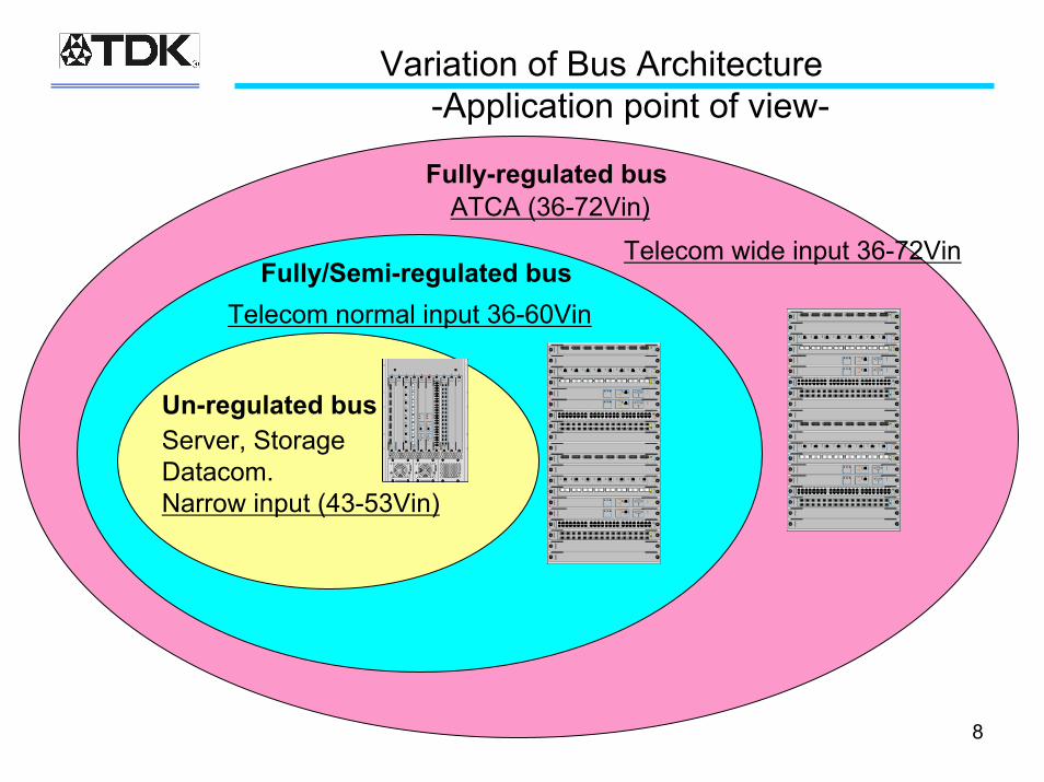
Variation of Bus Architecture-Application point of view-
Server, StorageDatacom.Narrow input (43-53Vin)
Telecom normal input 36-60Vin
Telecom wide input 36-72Vin
ATCA (36-72Vin)
Un-regulated bus
Fully/Semi-regulated bus
Fully-regulated bus

9
Relation between Input Sources and Bus Converters, and Bus Voltages
Input sources Bus converters Bus voltages
Narrow input(43-53Vin)
Telecom normal input(36-60Vin)
Telecom wide input,ATCA input(36-72Vin)
Un-regulated
Semi-regulated
Fully-regulated
4:1
5:1Un-regulated 12V
Un-regulated 9.6V
Semi-regulated 12V
Semi-regulated 9.6V
Fully-regulated 12V
Fully-regulated 9.6V
Fully-regulated 5V
Fully-regulated 3.3V
10
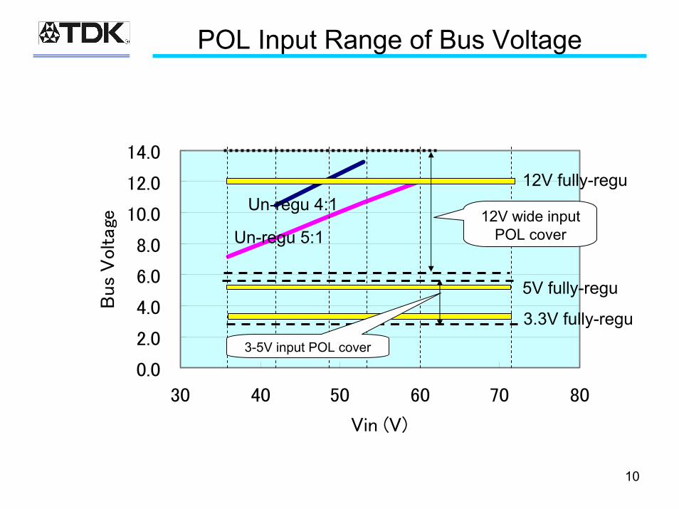
POL Input Range of Bus Voltage
0.0
2.0
4.0
6.0
8.0
10.0
12.0
14.0
30 40 50 60 70 80
Vin (V)
Bus
Voltage
12V fully-regu
5V fully-regu
3.3V fully-regu
Un-regu 4:1
Un-regu 5:112V wide input
POL cover
3-5V input POL cover

11
Stability Analysis of Bus Architecture

12
Considerations
• Evolution of the bus architecture allows flexibility and low cost concept in different applications.
• Because of many different types of bus architecture, the stability of the system has become an important issue.
• This report discusses stability for 3 types of bus converter and POL based on impedance analysis. To simplify the comparison, we have ignored the impact from internal interference between bus converter and POL.
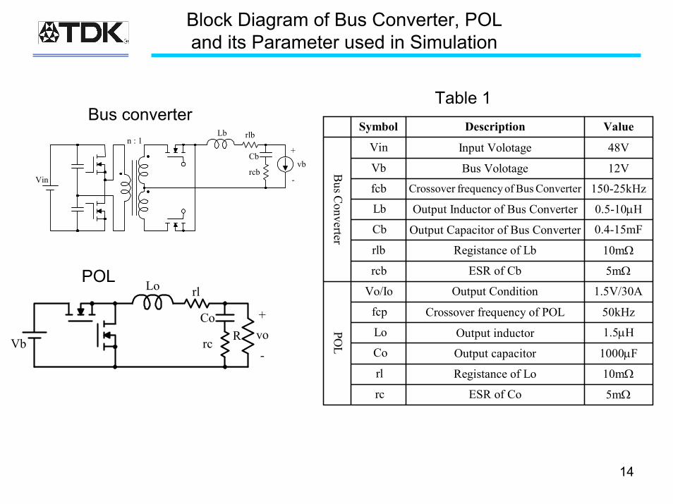
• The spec. used in this simulation of the power supply is 48Vin, bus voltage of 12V and POL of 1.5Vout/30Aout with 10 units in parallel. The detail value of the components such as output inductance, capacitance and cross-over frequency , etc are shown in table 1.
• The example of the simulation can not cover all phenomenon, butwe could leverage this method to practical applications.

13
Concept of 3 types of Bus Architectures
POL
48V
Un-regulated Bus converter
ZoZin
LoadPOL48V
Un-regulated Bus converter
ZoZin
Load12V, 9.6V
43-53V,36-60V
POL
48V
Semi-regulated Bus converter
PWM Controller
d
ZoZin
LoadPOL48V
Semi-regulated Bus converter
PWM Controller
d
ZoZin
Load12V,9.6V
43-53V,36-60V,36-72V
AC 100V/200V
POL
48V
AC/DC Bus Con.
POL
POL
Non Isolated DC-DC Con.
3.3V/10A
2.5V/20A
1.5V/30ALoad
Load
Load
POL
48VFull-regulated Bus converter
PWM Controller
d
ZoZin
LoadPOL48V
Full-regulated Bus converter
PWM Controller
d
ZoZin
Load
12V, 9.6V, 5V, 3.3V,
43-53V,36-60V,36-72V
14
Block Diagram of Bus Converter, POL and its Parameter used in Simulation
Table 1
n : 1
Vin
Lb
Cb
rlb
rcb
+
-
vb
Bus converter
Input Volotage
Symbol Description Value
Output ConditionVo/Io
Vin
1.5V/30A
48V
Vb
Output Inductor of Bus Converter
12V
Lb
Cb
rlb
rcb
Lo
Co
rl
rc
Registance of Lb
ESR of Cb
Output inductor
Output capacitor
Registance of Lo
ESR of Co
fcp Crossover frequency of POL
0.5-10µH
0.4-15mF
1.5µH
1000µF
50kHz
10mΩ
5mΩ
10mΩ
5mΩ
Output Capacitor of Bus Converter
Bus VolotageBus C
onverterPO
L
150-25kHzfcb Crossover frequency of Bus Converter
R
Lo
+
-vo
Co
rcVb
rlPOL

15
Output Impedance (Zo) of bus converter
( ) 21( )( ) b b b b
buso b b c b b L c L
bus
vZ s s L C r s L C r r r
i P s∆
= = + + +∆
1)()( 2 +++= CbLbbbb rrsCCLssP(Un-regu, Semi-regu)
Open loop
Where,
_
( )( )1 ( )
oo close
Z sZ s
T s=
+Closed loop (Fully-regu)
Where, T(s) is a transfer function of Bus converter
( ) ( ) ( )bc dvT H s G s PWM G s= ⋅ ⋅ ⋅
H(s): sense gain, Gc(s)=transfer function of the compensator,PWM: gain of the comparator, Gdv(s)=Vs/P(s) x (sCrc+1)

16
Input Impedance (Zin) of POL
2
//)1()()(
D
RrsC
rsLsZ
co
Lo
D
+++=
2)(
DRsZ n −=
R
Lo
+
-vo
Co
rcVb
rlZin
)(1
1)(
1)(1
)()(
1)(
1sTsZsT
sTsZsZ DNin +
⋅++
⋅=
100
101
102
103
104
105
106
-90
-45
0
45
90
Phas
e (
deg)
-20
-10
0
10
20
30
40
Mag
nitude
(dB
)
Bode Diagram
Frequency (Hz)
n=1
n=10
10 modules in parallel
Where, T(s) is a transfer function of POL
17
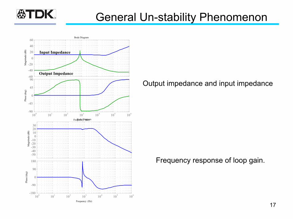
General Un-stability Phenomenon
100 101 102 103 104 105 106-90
-45
0
45
90
Phas
e (de
g)
-60
-40
-20
0
20
40
60
Mag
nitu
de (d
B)
Bode Diagram
Frequency (Hz)
Input Impedance
Output Impedance
Output impedance and input impedance
-50-40-30-20-10
0102030
Mag
nitu
de (d
B)
100 101 102 103 104 105 106-180
-90
0
90
180
Phas
e (de
g)
Bode Diagram
Frequency (Hz)
Frequency response of loop gain.
18
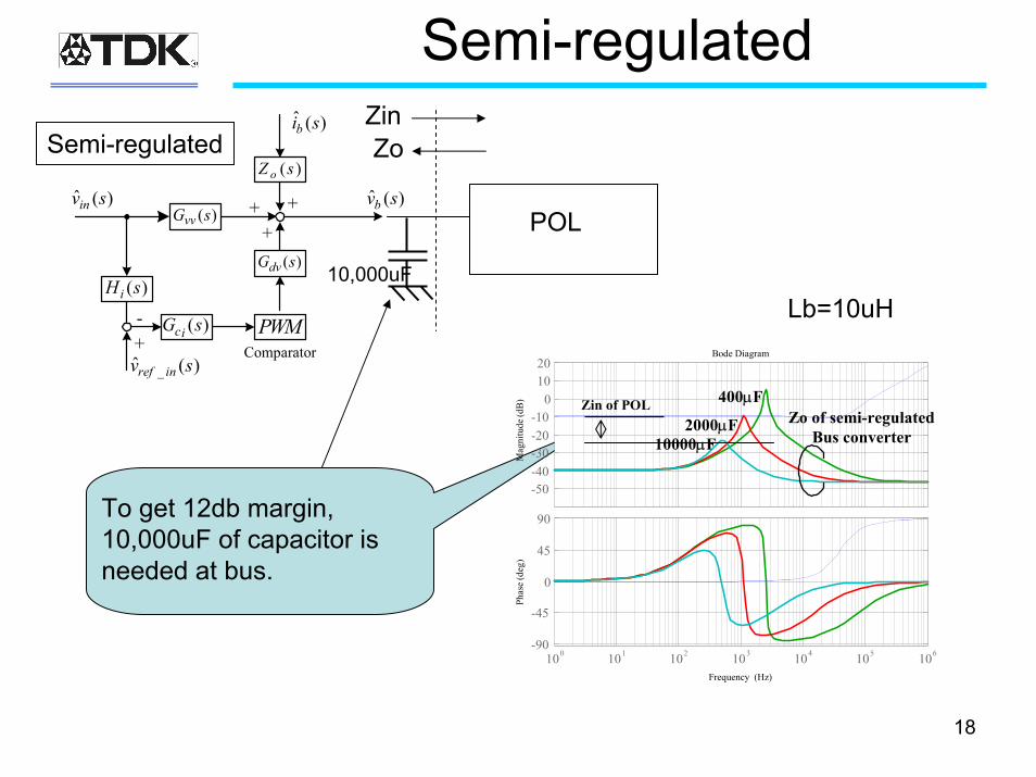
Semi-regulated
ˆ ( )bv s
ˆ ( )bi s
++
Comparator
( )dvG s
( )oZ s
PWM
+( )vvG s
( )ciG s
_ˆ ( )ref inv s+
( )iH s
-
ˆ ( )inv s
ZinZo
To get 12db margin, 10,000uF of capacitor is needed at bus.
10,000uF
Semi-regulated
POL
-50-40-30-20-10
01020
Mag
nitu
de (d
B)
100 101 102 103 104 105 106-90
-45
0
45
90Ph
ase
(deg
)
Bode Diagram
Frequency (Hz)
400µF
2000µF10000µF
Zin of POLZo of semi-regulated
Bus converter
Lb=10uH

19
Fully-regulated
-80
-60
-40
-20
0
20
Mag
nitu
de (d
B)
100 101 102 103 104 105 106-90
-45
0
45
90
135Ph
ase
(deg
)
Bode Diagram
Frequency (Hz)
400µF
5000µF1000µF
Zin of POL
Zo of full-regulatedBus converter
Cb and Zo : fcp=15kHz (Full-regulated case)
-80-70-60-50-40-30-20-10
01020
Mag
nitu
de (d
B)
100 101 102 103 104 105 106-90
-45
0
45
90
135
Phas
e (d
eg)
Bode Diagram
Frequency (Hz)
25kHz15kHz
150HzZin of POL
Zo of full-regulatedBus converter
ˆ ( )refv s
ˆ ( )ov s
ˆ ( )oi s
+
-
+
+Comparator
Sense Gain
Compensator
( )H s( )dvG s
( )oZ s
( )cG sPWM
+( )vvG sˆ ( )inv s
POL
ZinZo
Increase the cross over frequency of full-regulated bus converter damp the peak of Zo.
Further more, 2,000-3,000uF capacitor helpTo get 10deb margin.
2,000-3,000uFLb=10uH
Fully-regulated

20
Un-regulated
ˆ ( )refv s
ˆ ( )ov s
ˆ ( )oi s
+
-
+
+Comparator Compensator
( )dvG s
( )oZ s
( )cG sPWM
+( )vvG sˆ ( )inv s
*ˆ ( )ov s
-50-40-30-20-10
01020
Mag
nitu
de (d
B)
100 101 102 103 104 105 106-90
-45
0
45
90
Phas
e (d
eg)
Bode Diagram
Frequency (Hz)
10µH
2µH0.5µH
Zin of POL
Zo of un-regulatedBus converter
ZinZo
Un-regulated
POL
400uF
Un-regulated bus converter has small output inductance such as 0.5uH, so it is stable without large extra capacitor at the bus.
21
Conclusion
• Semi-regulated bus converter + POL– Need a large bus capacitor compare to un-regu. and fully-regu.
to be stable.– Can cover telecom normal input range (36-60Vin)
• Fully-regulated bus converter + POL– By adjusting a cross over frequency of bus converter, it can
reduce the bus capacitor for stability rather than semi-regu.– Can cover telecom wide input range (36-72Vin)
• Un-regulated bus converter + POL– Most stable (means less capacitor than others).– Can cover limited input range (narrow range of 43-53V)
• In a practical application, the bus capacitor should be designed by “ripple” , “transient response”, “stability”consideration.

22
Product for Bus Architecture

23
Bus ConvertersUn-regulated Bus converter (4:1)
iEB series : 12V/300W (Quarter brick size)
iQD series: 12V/150W (Eighth brick size)
Fully-regulated Bus Converter (Brick : 12V, 5V, 3.3V)
iEA seriesiQB series iQM series

24
POLs
12V wide input range (6-14V)
3-5.5V inputiAA series
iBA series
Vo= 0.75-3.63VIo =15A
PMH series
Vo=0.75-3.63V Io =8A
Vo= 0.75-5VIo = 16A