stability of polymer light-emitting diodes - … bound... · stability of polymer light-emitting...
TRANSCRIPT
Philips J. Res. 51 (1998) 511-525
STABILITY OF POLYMER LIGHT-EMITTING DIODES
by A.I.M. BERNTSEN, P.VAN DE WEIJER, Y. CROONEN,C.T.H.F. LIEDENBAUM and I.I.M. VLEGGAAR
Philips Research Laboratories, Prof Holstlaan 4, 5656 AA Eindhoven, The Netherlands
AbstractIn this paper, we report on the lifetime of polymer LEDs fabricated atPhilips Research. For single-layer LEDS, we find that the operationallife-time in nitrogen gas is limited by the stability of the indium-tin-oxide(ITO) anode. By using a polymeric capping layer for the ITO, we obtainmore stable devices. In air, the lifetime is limited by black spot forma-tion. Small pinholes in the cathode layer are the origins of the blackspots. Water or oxygen may diffuse through these pinholes and reactwith the cathode, causing degradation. By encapsulating the devices wecan prevent black spot formation. Our present 8 cm2 devices have lifetimesof many thousands of hours at daylight visibility under ambient conditions.
Keywords: electroluminescence, photoluminescence, light-emittingdiodes, polymers, lifetime, carbonyl groups.
1. Introduetion
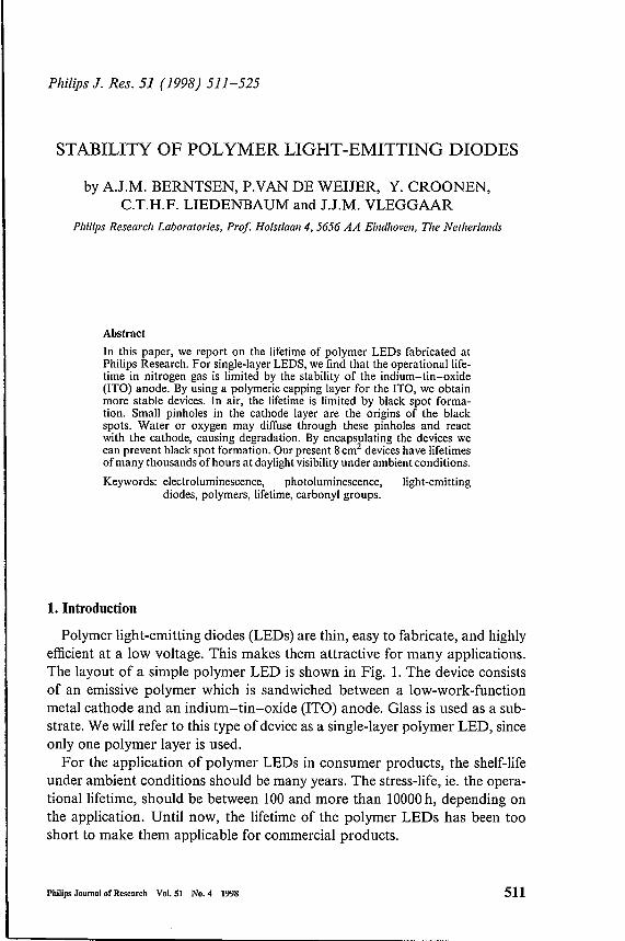
Polymer light-emitting diodes (LEDs) are thin, easy to fabricate, and highlyefficient at a low voltage. This makes them attractive for many applications.The layout of a simple polymer LED is shown in Fig. 1. The device consistsof an emissive polymer which is sandwiched between a low-work-functionmetal cathode and an indium-tin-oxide (ITO) anode. Glass is used as a sub-strate. We will refer to this type of device as a single-layer polymer LED, sinceonly one polymer layer is used.For the application of polymer LEDs in consumer products, the shelf-life
under ambient conditions should be many years. The stress-life, ie. the opera-tional lifetime, should be between 100 and more than 10000h, depending onthe application. Until now, the lifetime of the polymer LEDs has been tooshort to make them applicable for commercial products.
Philip. Journni of Research Vol. SI No.4 1998 511
A.J.M. Berntsen et al.
PolymerITO "'''':'7~''f1;:)..~-T;:;!'·''''''lrI:l'l\..,_:.t::'"'!:77:'''''~'lt';'''''..• -., T '
Metal
Fig. 1. Device layout of a single-layer polymer LED, showing the ITO anode, the emissive poly-mer, and the metal cathode.
Here, we report on the lifetime of polymer LEDs fabricated at Philips. Wedivide the lifetime of the LEDs into an intrinsic lifetime, which is obtainedunder inert-gas conditions, and a practical (actual) lifetime, which is obtainedfor ambient conditions. For unencapsulated devices the latter lifetime is short,due to degradation effects induced by water and oxygen.
This paper is organized as follows. In Sec. 2, the lifetime measurement set-up is described. We then discuss lifetime data in Sec. 3. In Sec. 4, we presentfailure analysis for single-layer devices, and we systematically investigate thepossible causes of ageing of the three layers involved: the polymer, the cath-ode and the anode. It is found that the intrinsic lifetime is limited by thestability of the ITO anode, while the practical lifetime is limited by blackspot formation caused by oxidation of the cathode. In Sec. 5, it is shownthat double-layer devices, in which a polymeric capping layer for the ITO isused, are more stable. We also demonstrate that black spots can be avoidedby using a proper encapsulation method. Conclusions are summarized in Sec. 6.
2. Lifetime measurements
Measurements of the operationallifetimes were performed under DC con-ditions at constant current. Lifetime is defined as the time elapsed until theemission of the device has decreased to 50% of the initial intensity. Deviceswere tested in a nitrogen glovebox (water and oxygen content at ppm level),in an oven (high temperature, low humidity), or in a climate chamber (hightemperature, high humidity). The glovebox and climate chambers can accom-modate more than 100 sample holders. Each sample holder is equipped with aphotodiode for measurement of the light output, and a driver consisting of apower supply and light-measurement card. The sample holders and drivers arearranged in units of 16 pieces. For each unit, a microprocessor performs dataacquisition (voltage, device current and photocurrent) sequentially. The var-ious units work in parallel. Data storage and control is performed with aPC, using LabVIEW control software.
512 Philips Journal of Research Vol. SI No.4 [998
Stability of polymer light-emitting diodes
o
-0Fig. 2. Poly(dialkoxy-p-phenylenevinylene).
3. The intrinsic lifetime of single-layer devices
Our first type of polymer LED consisted of a single polymer layer,poly(dialkoxy-p-phenylenevinylene) (see Fig. 2), which was sandwichedbetween a metal cathode and an ITO anode. The typical thickness of aIllayerswas 100nm. The active area ranged from 0.04 to Icrrr'. The devices were notencapsulated. The operational lifetimes, as measured in a glovebox system,were a few hours.
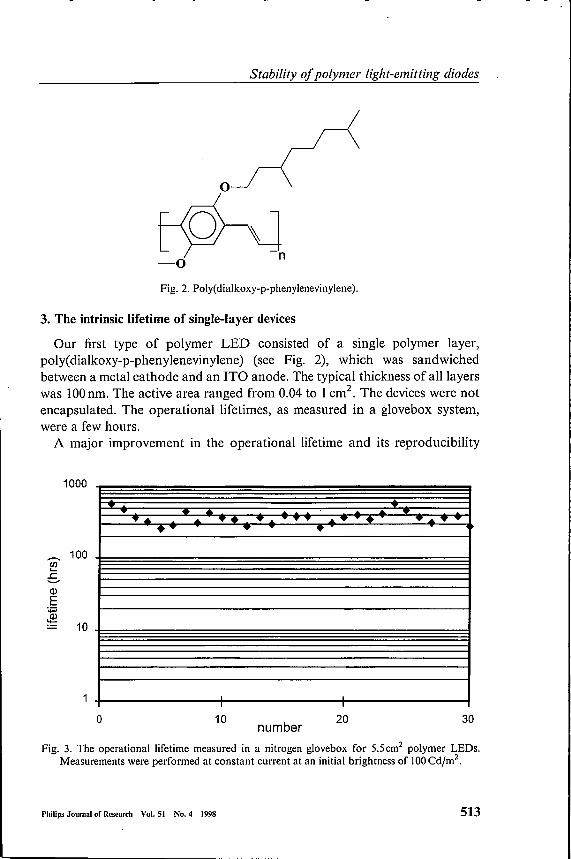
A major improvement in the operational lifetime and its reproducibility
Fig. 3. The operational lifetime measured in a nitrogen glovebox for 5.5cm2 polymer LEDs.Measurements were performed at constant current at an initial brightness of 100Cd/m2•
1000
en 100....E-IDE:;:;
~ 10
o 10number
20 30
Philips Journalof Research Vol. SI No.4 1998 513
A.J.M. Berntsen et al.
1.4
1.2 -- t= Omin (a)
-- t= 10minQ) 1.0 _-- t=20minu
---- t = 30 mins:: 0.8ro .......... t>120 min...0....0 0.6en...0ro 0.4
0.2
0.0100 200 300 400 500 600 700
wavelength (run)
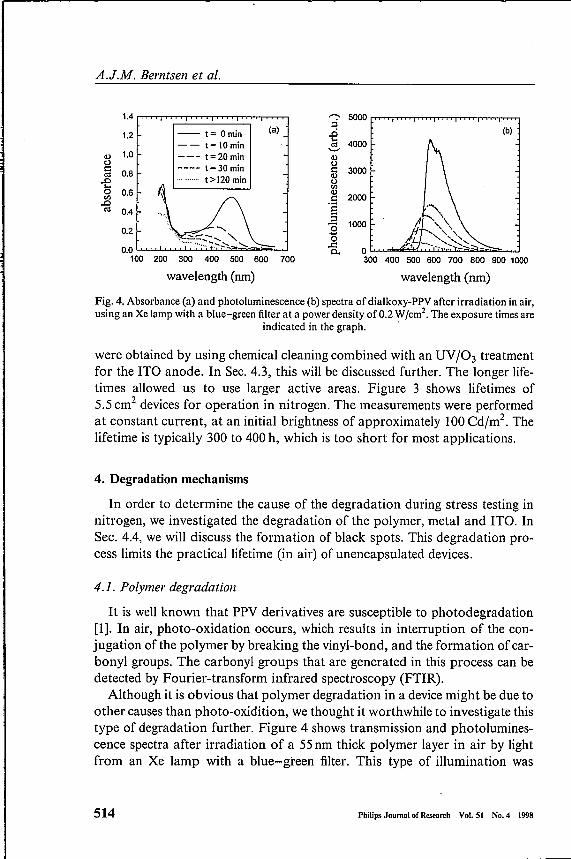
Fig. 4. Absorbance (a) and photoluminescence (b) spectra of dialkoxy-PPV after irradiation in air,using an Xe lamp with a blue-green filter at a power density of 0.2 Wfcm2• The exposure times are
indicated in the graph. .
were obtained by using chemical cleaning combined with an UV f03 treatmentfor the ITO anode. In Sec. 4.3, this will be discussed further. The longer life-times allowed us to use larger active areas. Figure 3 shows lifetimes of5.5 crrr' devices for operation in nitrogen. The measurements were performedat constant current, at an initial brightness of approximately 100Cd/m", Thelifetime is typically 300 to 400 h, which is too short for most applications.
4. Degradation mechanisms
In order to determine the cause of the degradation during stress testing innitrogen, we investigated the degradation of the polymer, metal and ITO. InSec. 4.4, we will discuss the formation of black spots. This degradation pro-cess limits the practicallifetime (in air) of unencapsulated devices.
4.1. Polymer degradation
It is well known that PPV derivatives are susceptible to photodegradation[1]. In air, photo-oxidation occurs, which results in interruption of the con-jugation of the polymer by breaking the vinyl-bond, and the formation of car-bonyl groups. The carbonyl groups that are generated in this process can bedetected by Fourier-transform infrared spectroscopy (FTIR).
Although it is obvious that polymer degradation in a devicemight be due toother causes than photo-oxidition, we thought it worthwhile to investigate thistype of degradation further. Figure 4 shows transmission and photolumines-cence spectra after irradiation of a 55nm thick polymer layer in air by lightfrom an Xe lamp with a blue-green filter. This type of illumination was
514 Philip. Journal of Research Vol. SI No.4 1998
Stability of polymer light-emitting diodes
1.0
air, y = 1.6 10'"(a)
0.8t::0'iii 0.6til
'ë0.4tilc
'".......0.2 -- measured data
--fit0.0
0 300 600 900 1200
time (s)
1.0air, y = 1.6 10'" (b)
0.8t::0'r.;; 0.6 HP vapour, t= 7.1 10.7til
'ërn 0.4t::'"....+'"
p = io" mbar,0.2t= 1.7 10.7
0.00 4000 8000 12000
time (s)
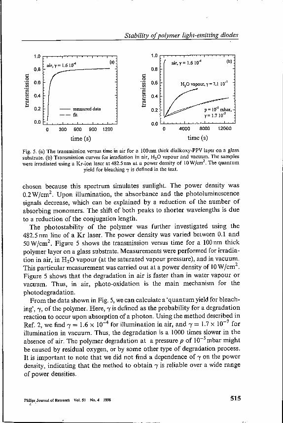
Fig. 5. (a) The transmission versus time in air for a 100nm thick dialkoxy-PPV layer on a glasssubstrate. (b) Transmission curves for irradiation in air, H20 vapour and vacuum. The sampleswere irradiated using a Kr-ion laser at 482.5nm at a power density of IOWjcm2
• The quantumyield for bleaching '"Y is defined in the text.
chosen because this spectrum simulates sunlight. The power density was0.2Wjcm2• Upon illumination, the absorbance and the photoluminescencesignals decrease, which can be explained by a reduction of the number ofabsorbing monomers. The shift of both peaks to shorter wavelengths is dueto a reduction of the conjugation length.The photostability of the polymer was further investigated using the
482.5 nm line of a Kr laser. The power density was varied between 0.1 and50Wjcm2• Figure 5 shows the transmission versus time for a 100nm thickpolymer layer on a glass substrate. Measurements were performed for irradia-tion in air, in H20 vapour (at the saturated vapour pressure), and in vacuum.This particular measurement was carried out at a power density of IOWjcm2
.
Figure 5 shows that the degradation in air is faster than in water vapour orvacuum. Thus, in air, photo-oxidation is the main mechanism for thephotodegradation.
From the data shown in Fig. 5,wecan calculate a 'quantum yield for bleach-ing', Î, of the polymer. Here, 'Y is defined as the probability for a degradationreaction to occur upon absorption of a photon. Using the method described inRef. 2, we find 'Y = 1.6 X 10⁻⁴ for illumination in air, and Î = 1.7 X 10⁻⁷ forillumination in vacuum. Thus, the degradation is a 1000 times slower in theabsence of air. The polymer degradation at a pressure p of 10-5 mbar mightbe caused by residual oxygen, or by some other type of degradation process.It is important to note that we did not find a dependence of Î on the powerdensity, indicating that the method to obtain 'Y is reliable over a wide rangeof power densities.
PhifPs.Joumo. of Research Vol. 51 No.4 1998 515
A.J.M. Berntsen et al.
!="" 0.8
P+ ·0.6~.._.,I
E-<n 0.4 -
~n0.2
0.00
T_-- R
200 400 600 800 1000
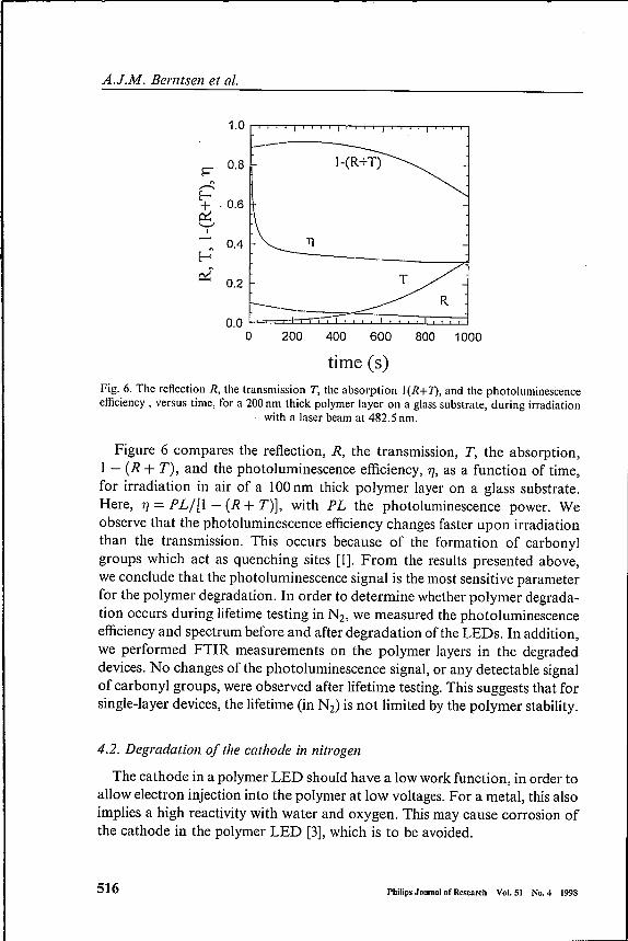
time Cs)Fig. 6. The reflection R, the transmission T, the absorption I(R+1), and the photoluminescenceefficiency, versus time, for a 200 nm thick polymer layer on a glass substrate, during irradiation
with a laser beam at 482.5 nm.
Figure 6 compares the reflection, R, the transmission, T, the absorption,1 - (R + T), and the photoluminescence efficiency, 7], as a function of time,for irradiation in air of a 100nm thick polymer layer on a glass substrate.Here, 7] = PL/[I - (R + T)], with PL the photoluminescence power. Weobserve that the photoluminescence efficiency changes faster upon irradiationthan the transmission. This occurs because of the formation of carbonylgroups which act as quenching sites [1]. From the results presented above,we conclude that the photoluminescence signal is the most sensitive parameterfor the polymer degradation. In order to determine whether polymer degrada-tion occurs during lifetime testing in N2, we measured the photoluminescenceefficiencyand spectrum before and after degradation ofthe LEDs. In addition,we performed FTIR measurements on the polymer layers in the degradeddevices. No changes of the photoluminescence signal, or any detectable signalof carbonyl groups, were observed after lifetime testing. This suggests that forsingle-layer devices, the lifetime (in N2) is not limited by the polymer stability.
516 Philips Journal of Research Vol. SI No.4 1998
4.2. Degradation of the cathode in nitrogen
The cathode in a polymer LED should have a low work function, in order toallow electron injection into the polymer at low voltages. For a metal, this alsoimplies a high reactivity with water and oxygen. This may cause corrosion ofthe cathode in the polymer LED [3],which is to be avoided.
Stability of polymer light-emitting diodes
~c
sputter time
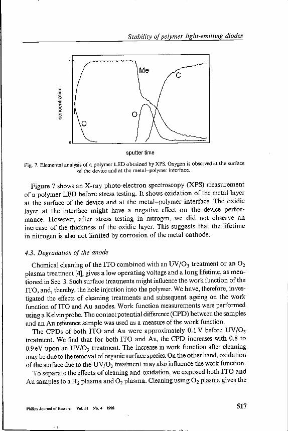
Fig. 7. Elemental analysis of a polymer LED obtained by XPS. Oxygen is observed at the surfaceof the device and at the metal-polymer interface.
Figure 7 shows an X-ray photo-electron spectroscopy (XPS) measurementof a polymer LED before stress testing. It shows oxidation of the metallayerat the surface of the device and at the metal-polymer interface. The oxidiclayer at the interface might have a negative effect on the device perfor-mance. However, after stress testing in nitrogen, we did not observe anincrease of the thickness of the oxidic layer. This suggests that the lifetimein nitrogen is also not limited by corrosion of the metal cathode.
4.3. Degradation of the anode
Chemical cleaning of the ITO combined with an UV/03 treatment or an O2
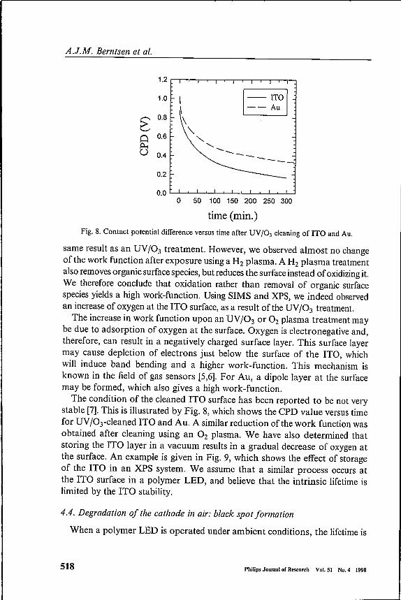
plasma treatment [4],gives a low operating voltage and a long lifetime, as men-tioned in Sec. 3. Such surface treatments might influencethe work function of theITO, and, thereby, the hole injection into the polymer.We have, therefore, inves-tigated the effects of cleaning treatments and subsequent ageing on the workfunction ofITO and Au anodes. Work function measurements were performedusing a Kelvin probe. The contact potential difference(CPD) between the samplesand an Au referencesample was used as a measure of the work function.The CPDs of both ITO and Au were approximately 0.1 V before UV /03
treatment. We find that for both ITO and Au, the CPD increases with 0.8 to0.9eV upon an UV/03 treatment. The increase in work function after cleaningmay be due to the removal of organic surface species.On the other hand, oxidationof the surface due to the UV/03 treatment mayalso influence the work function.To separate the effects of cleaning and oxidation, we exposed both ITO and
Au samples to a H2 plasma and O2 plasma. Cleaning using O2 plasma gives the
Philips Journalof Research Vol. SI No.4 1998 517
A.J.M. Berntsen et al.
1.2
1.0 I~~ u
~0.8 \ -,
Cl 0.6 <,~ <,U 0.4
-.._ __
0.2
0.00 50 100 150 200 250 300
time (min.)Fig. 8. Contact potential difference versus time after UV/03 cleaning of ITO and Au.
same result as an UV/03 treatment. However, we observed almost no changeofthe work function after exposure using a H2 plasma. A H2 plasma treatmentalso removesorganic surface species, but reduces the surface instead of oxidizingit.We therefore conclude that oxidation rather than removal of organic surfacespecies yields a high work-function. Using SIMS and XPS, we indeed observedan increase of oxygen at the ITO surface, as a result ofthe UV/03 treatment.The increase in work function upon an UV/03 or O2 plasma treatment may
be due to adsorption of oxygen at the surface. Oxygen is electronegative and,therefore, can result in a negatively charged surface layer. This surface layermay cause depletion of electrons just below the surface of the ITO, whichwill induce band bending and a higher work-function. This mechanism isknown in the field of gas sensors [5,6]. For Au, a dipole layer at the surfacemay be formed, which also gives a high work-function.
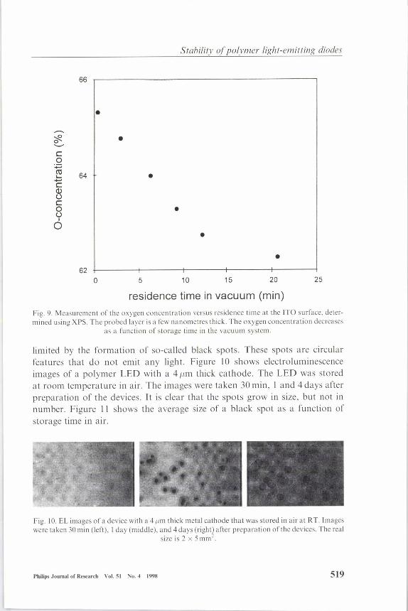
The condition of the cleaned ITO surface has been reported to be not verystable [7].This is illustrated by Fig. 8, which shows the CPD value versus timefor UV/Orcleaned ITO and Au. A similar reduction ofthe work function wasobtained after cleaning using an O2 plasma. We have also determined thatstoring the ITO layer in a vacuum results in a gradual decrease of oxygen atthe surface. An example is given in Fig. 9, which shows the effect of storageof the ITO in an XPS system. We assume that a similar process occurs atthe ITO surface in a polymer LED, and believe that the intrinsic lifetime islimited by the ITO stability.
4.4. Degradation of the cathode in air: black spot formation
When a polymer LED is operated under ambient conditions, the lifetime is
518 Philips Journalof Research Vol. SI No.4 1998
Stability of polymer light-emitting diodes
66
•::$!. •0.._...c0~CU 64 •I-......CQ)ÜC0 •o,0
•
Ph_ilipsJournalof Research Vol. 51 NO.4 1998 519
•62
o 5 10 15 20 25
residence time in vacuum (min)Fig. 9. Measurement of the oxygen concentration versus residence time at the ITO surface, deter-mined using XPS. The probed layer is a few nanometres thick. The oxygen concentration decreases
as a function of storage time in the vacuum system.
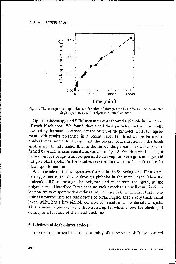
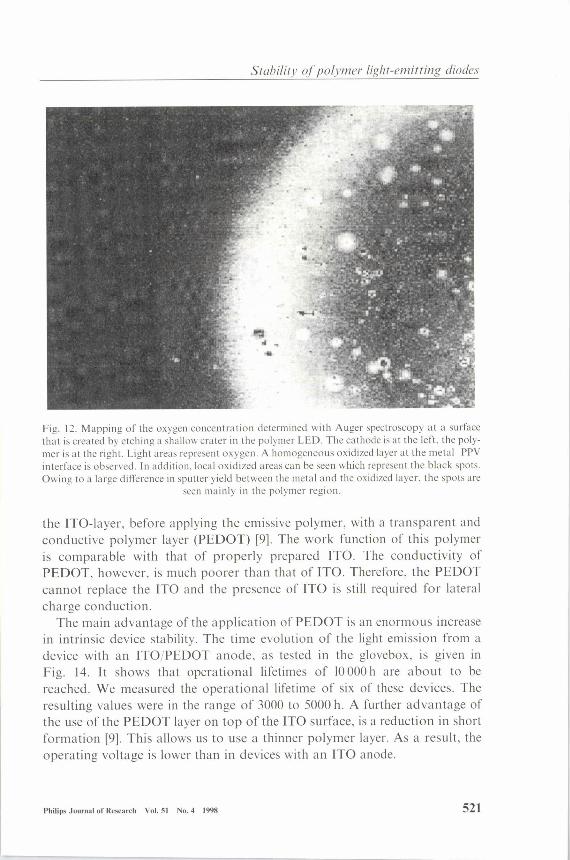
limited by the formation of so-called black spots. These spots are circularfeatures that do not emit any light. Figure 10 shows electroluminescenceimages of a polymer LED with a 4 f.Lm thick cathode. The LED was storedat room temperature in air. The images were taken 30 min, I and 4 days afterpreparation of the devices. It is clear that the spots grow in size, but not innumber. Figure 11 shows the average size of a black spot as a function ofstorage time in air.
Fig. 10. EL images of a device with a4 f.L11l thick metal cathode that was stored in air at RT.Imageswere taken 30 min (left), I day (middle), and 4days (right) after preparation ofthe devices. The real
size is 2 x 5mm2
A.J.M. Berntsen et al.
-.. 0.15N
ê'--'0 0.10N.-Cl)......00..Cl)
~0.05
ti:!.........,.0
0.000 10000 20000 30000
time (min.)Fig. 11. The average black spot size as a function of storage time in air for an unencapsulated
single-layer device with a 4 jJ.mthick metal cathode.
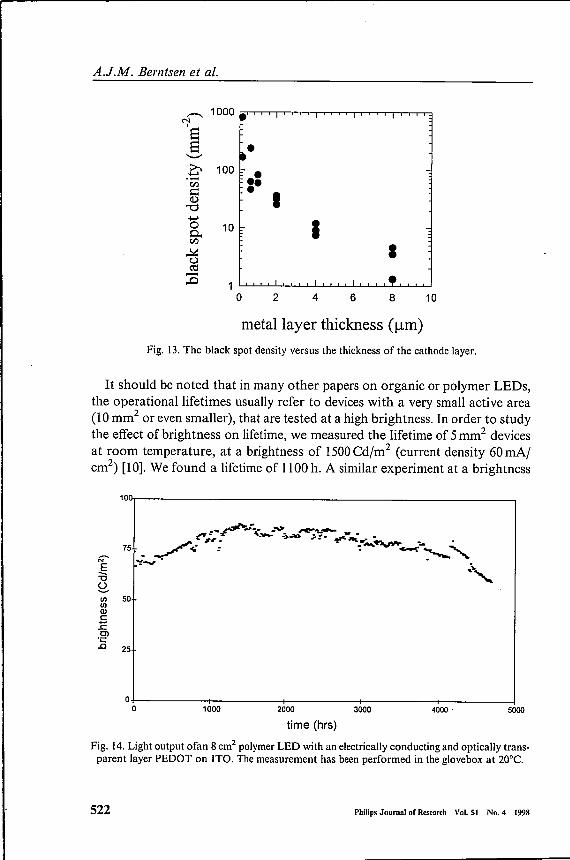
Optical microscopy and SEM measurements showed a pinhole in the centreof each black spot. We found that small dust particles that are not fullycovered by the metal electrode, are the origin of the pinholes. This is in agree-ment with results presented in a recent paper [8]. Electron probe micro-analysis measurements showed that the oxygen concentration in the blackspots is significantly higher than in the surrounding areas. This was also con-firmed by Auger measurements, as shown in Fig. 12.We observed black spotformation for storage in air, oxygen and water vapour. Storage in nitrogen didnot give black spots. Further studies revealed that water is the main cause forblack spot formation.
We conclude that black spots are formed in the following way. First wateror oxygen enters the device through pinholes in the metal layer. Then themolecules diffuse through the polymer and react with the metal at thepolymer-metal interface. It is clear that such a mechanism will result in circu-lar non-emissive spots with a radius that increases in time. The fact that a pin-hole is a prerequisite for black spots to form, implies that a very thick metallayer, which has a low pinhole density, will result in a low density of spots.This is indeed observed, as is shown in Fig. 13, which shows the black spotdensity as a function of the metal thickness.
5. Lifetimes of double-layer devices
In order to improve the intrinsic stability of the polymer LEDs, we covered
520 Philips Journal of Research Vol. SI No.4 1998
Philips Journalof Research Vol. SI No.4 1998 521
Stability ofpolymer light-emitting diodes
Fig. 12. Mapping of the oxygen concentration determined with Auger spectroscopy at a surfacethat is created by etching a shallow crater in the polymer LED. The cathode is at the left, the poly-mer is at the right. Light areas represent oxygen. A homogeneous oxidized layer at the metal-PPVinterface is observed. In addition, local oxidized areas can be seen which represent the black spots.Owing to a large difference in sputter yield between the metal and the oxidized layer. the spots are
seen mainly in the polymer region.
the ITO-layer, before applying the emissive polymer, with a transparent andconductive polymer layer (PEDOT) [9]. The work function of this polymeris comparable with that of properly prepared ITO. The conductivity ofPEDOT, however, is much poorer than that of ITO. Therefore, the PEDOTcannot replace the ITO and the presence of ITO is still required for lateralcharge conduction.
The main advantage of the application of PEDOT is an enormous increasein intrinsic device stability. The time evolution of the light emission from adevice with an ITO/PEDOT anode, as tested in the glovebox, is given inFig. 14. It shows that operational lifetimes of 10000 h are about to bereached. We measured the operational lifetime of six of these devices. Theresulting values were in the range of 3000 to 5000 h. A further advantage ofthe use of the PEDOT layer on top of the ITO surface, is a reduction in shortformation [9]. This allows us to use a thinner polymer layer. As a result, theoperating voltage is lower than in devices with an ITO anode.
A.J.M. Berntsen el al.
....--. 1000 " I<il88 ,.<;»
0 100 ••.-e/} ••~ I(!)"'d-+->0 100..e/}
~~.......,.0 1
0 2
I
II
,.4 6 8 10
metallayer thickness (urn)Fig. 13.The black spot density versus the thickness of the cathode layer.
It should be noted that in many other papers on organic or polymer LEDs,the operationallifetimes usually refer to devices with a very small active area(10mrrr' or even smaller), that are tested at a high brightness. In order to studythe effect of brightness on lifetime, we measured the lifetime of 5mrrr' devicesat room temperature, at a brightness of 1500Cd/rrr' (current density 60mAlcm2
) [10].We found a lifetime of 1100 h. A similar experiment at a brightness
101~-------- ~
Ë=a8(/)(/)
aJc:.:ECl.;::.0
50
25
O~---------r--------~----------;---------~-- ~o 1000 2000 3000 4000 . 5000
time (hrs)
Fig. 14. Light output ofan 8 cm2 polymer LED with an electrically conducting and optically trans-parent layer PEDOT on ITO. The measurement has been performed in the glovebox at 20°C.
522 Philips Journalof Research Vol. SI No.4 1998
Stability of polymer light-emitting diodes
30~--------------------------------------------------~
N.€ 20"C
~IIIIIIQ)c:E.g> 10.0
o 1000 2000 3000 40000+----------r---------+----------+----------r---------4
5000time (hrs)
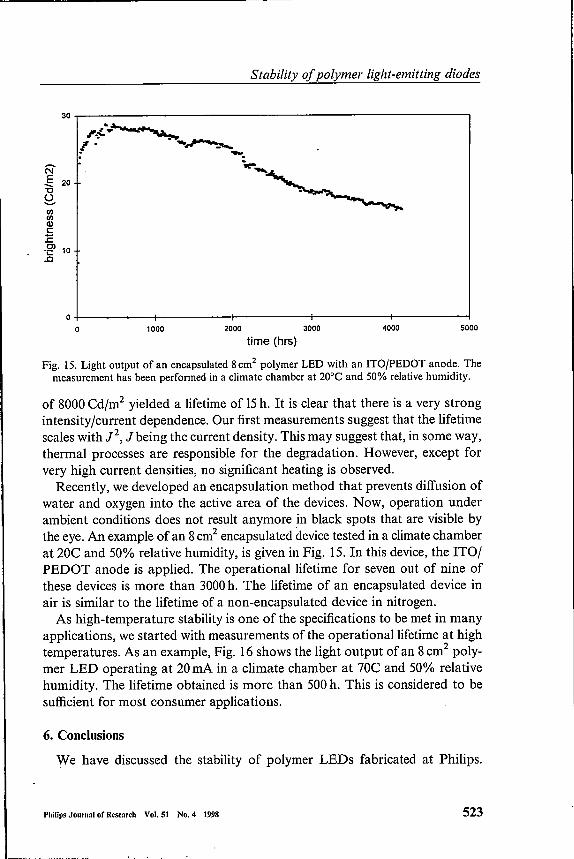
Fig. IS. Light output of an encapsulated 8cm2 polymer LED with an ITO/PEDOT anode. Themeasurement has been performed in a climate chamber at 20°C and 50% relative humidity.
of 8000 Cd/m2 yielded a lifetime of 15h. It is clear that there is a very strongintensity/current dependence. Our first measurements suggest that the lifetimescales with J2, Jbeing the current density. This may suggest that, in some way,thermal processes are responsible for the degradation. However, except forvery high current densities, no significant heating is observed.
Recently, we developed an encapsulation method that prevents diffusion ofwater and oxygen into the active area of the devices. Now, operation underambient conditions does not result anymore in black spots that are visible bythe eye. An example of an 8cm2 encapsulated device tested in a climate chamberat 20C and 50% relative humidity, is given in Fig. IS. In this device, the ITO/PEDOT anode is applied. The operational lifetime for seven out of nine ofthese devices is more than 3000h. The lifetime of an encapsulated device inair is similar to the lifetime of a non-encapsulated device in nitrogen.As high-temperature stability is one of the specifications to be met in many
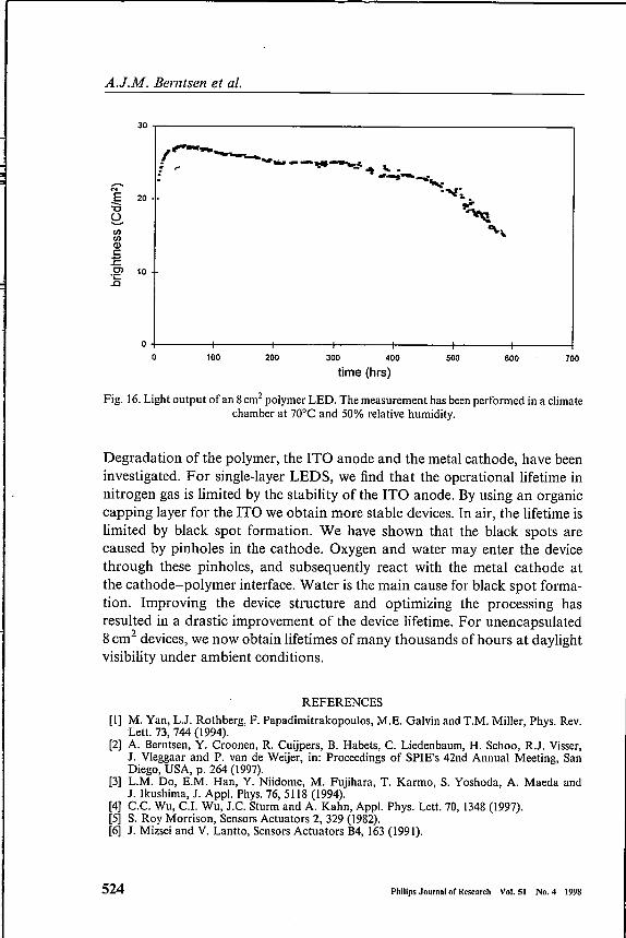
applications, we started with measurements of the operationallifetime at hightemperatures. As an example, Fig. 16 shows the light output of an 8cm2 poly-mer LED operating at 20mA in a climate chamber at 70C and 50% relativehumidity. The lifetime obtained is more than 500h. This is considered to besufficient for most consumer applications.
6. Conclusions
We have discussed the stability of polymer LEDs fabricated at Philips.
Philip. Journal of Research Vol. SI No.4 1998 523
A.J.M. Berntsen et al.
30~---------------------- ~
~~ 20
~VIVIQ)c::E:Cl 10:E
O+-----~r_----_+------_r------+_----~r_----_+----~100 200 300 400
time (hrs)500 600 700
Fig. 16.Light output ofan 8cm2 polymer LED. The measurement has been performed in a climatechamber at 70°C and 50% relative humidity.
Degradation of the polymer, the ITO anode and the metal cathode, have beeninvestigated. For single-layer LEDS, we find that the operational lifetime innitrogen gas is limited by the stability of the ITO anode. By using an organiccapping layer for the ITO we obtain more stable devices. In air, the lifetime islimited by black spot formation. We have shown that the black spots arecaused by pinholes in the cathode. Oxygen and water may enter the devicethrough these pinholes, and subsequently react with the metal cathode atthe cathode-polymer interface. Water is the main cause for black spot forma-tion. Improving the device structure and optimizing the processing hasresulted in a drastic improvement of the device lifetime. For unencapsulated8 cm2 devices, we now obtain lifetimes of many thousands of hours at daylightvisibility under ambient conditions.
REFERENCES[I] M. Yan, L.J. Rothberg, F. Papadimitrakopoulos, M.E. Galvin and T.M. Miller, Phys. Rev.
Lett. 73, 744 (1994).[2] A. Berntsen, Y. Croonen, R. Cuijpers, B. Habets, C. Liedenbaum, H. Schoo, R.J. Visser,
J. Vleggaar and P. van de Weijer, in: Proceedings of SPIE's 42nd Annual Meeting, SanDiego, USA, p. 264 (1997).
[3] L.M. Do, E.M. Han, Y. Niidome, M. Fujihara, T. Karmo, S. Yoshoda, A. Maeda andJ. Ikushima, J. Appl. Phys. 76, 5118 (1994).
[4] C.C. Wu, C.l. Wu, J.C. Sturm and A. Kahn, Appl. Phys. Lett. 70, 1348 (1997).[5] S. Roy Morrison, Sensors Actuators 2, 329 (1982).[6] J. Mizsei and V. Lantto, Sensors Actuators B4, 163 (1991).
524 Philips Journalof Research Vol. SI No.4 1998
Philips Journalof Research Vol. SI No.4 1998 525
Stability of polymer light-emitting diodes
[7] S. Karg, P.J. Broek and J.C. Scott, Appl. Phys. Lett. 70, 2067 (1997).[8] J. McElvain, H. Antoniadis, M.R. Hueschen, J.N. Miller, D.M. Roitman, J.R. Sheats and
R.L. Moon, J. App!. Phys. 80, 6002 (1996).[9] S. Karg, J.C. Scott, J.R. Salem and M. Angelopoulos, Synthetic Metals 80, I11 (1996).[10] C. Liedenbaum, Y. Croonen, P. van de Weijer, J. Vleggaar and H. Schoo, ICEL'97,
Fukuoka, Japan Synthetic Metals, to be published.
Authors Biographies
Arjan Berntsen was born in 1967 in Amsterdam. From 1985 to 1989he studied physics at Amster-dam University. In 1990,he started his Ph.D. studies at Utrecht University, investigating the struc-tural disorder in amorphous silicon. In its hydrogenated form, this material is suited for solar cells,transistors and diodes. He obtained his Ph.D. in 1993. Since 1994, he works at Philips on the sta-bility of polymer light-emitting diodes.
Peter van de Weijer studied chemistry at the State University of Utrecht (1968-1974). In his thesis,at the Twente University of Technology (1977), he described acid-base properties of aza-aro-matics, as investigated by nuclear magnetic resonance. At the Philips Research Laboratories(1977) he started in the gaseous electronics group, where he performed laser-diagnostic measure-ments on low-pressure mercury discharges. Then, in the spectroscopy group he applied similartechniques on chemical vapour deposition systems and gas detectors for chromatography. Inthe department for analytical chemistry, he was involved in inductively-coupled plasma mass spec-trometry and X-ray fluorescence. Since 1994,he has worked in the polymers and organic chemistrygroup, researching the stability of polymer light-emitting diodes.
Yvo Croonen was born in 1958 in Neerpelt, Belgium. From 1976-1980 he studied chemistry at theK.U.Leuven. He started his Ph.D. in 1981at K.U.Leuven, investigating the characteristics of aqu-eous anionic micelles by means of emission spectrometry. He obtained his Ph.D. in 1985. SinceJuly 1985, he has worked at Philips CFT on the development and implementation of litho-graphic, CVD and PVD production processes. In 1995, he joined the polymer light-emitting diodeproject, where he his mainly concerned with the manufacturability of polymer LED devices.
Coen Liedenbaumjoined the Philips Research Laboratories in 1989,and started to work on visiblediode lasers. Other projects in optical recording and high-speed optical transmission, preceded thecurrent project of poly~er LEDs, where he is responsible for development coordination.
Jeroen Vleggaar was born in Amsterdam in 1965.He studied chemical technology at the Univer-sity of Twente from 1983 to 1988. After his militairy service, he did his Ph.D. at the University ofLeiden in photochemistry, from 1990to 1994.The subject ofthe thesis was the photochemistry andphotophysics ofphotoresist. Since December 1994,he has worked at Philips Research on polymerLEDs.