staircase multicarrier spwm technique for nine level cascaded inverter
TRANSCRIPT

8/10/2019 Staircase Multicarrier SPWM Technique for Nine Level Cascaded Inverter
http://slidepdf.com/reader/full/staircase-multicarrier-spwm-technique-for-nine-level-cascaded-inverter 1/8
2013 International Conference on Power, Energy and Control (ICPEC)
978-1-4673-6030-2/13/$31.00 ©2013 IEEE668
Staircase Multicarrier SPWM Technique for NineLevel Cascaded Inverter
R.Nagarajan
Dept of Electrical and Electronics Engineering,Raja College of Engg. & Tech,
Madurai. Tamilnadu, India.e-mail:[email protected]
M. SaravananDept of Electrical and Electronics Engineering,
Thiagarajar College of Engineering.,Madurai. Tamilnadu, India.
e-mail:[email protected]
Abstract — In this paper, novel pulse width modulation techniquewhich use staircase carrier waveform is proposed for nine levelcascaded inverter. In staircase carrier waveform, differenttechniques such as phase disposition (PD), inverted phasedisposition (IPD), phase opposition disposition (POD) andalternative phase opposition disposition (APOD) areimplemented. The fundamental output voltage and harmonics
obtained in each method are compared with the output waveformobtained with the triangular carrier waveform. The proposedswitching technique enhances the fundamental component of theoutput voltage and improves total harmonic distortion. Thedifferent PWM methodologies adopting the constant switchingfrequency multicarrier are simulated for a 1KW, 3 φ inverterusing MATLAB/SIMULINK. The effect of switching frequencyon the fundamental output voltage and harmonics are alsoanalyzed.
Keywords: Sinusoidal Pulse Width Modulation (SPWM), Staircase Multicarrier SPWM (SCMC SPWM), Triangular Multicarrier SPWM (TMC SPWM), Total Harmonic Distortion (THD).
I. I NTRODUCTION Multilevel inverter is an effective solution for increasing
power and reducing harmonics of ac waveform [1]. Multilevelinverters are suitable for high voltage and high powerapplications due to their ability to synthesize waveforms with
better harmonics and important for power electronicsapplications such as flexible ac transmission systems,renewable energy sources, uninterruptible power supplies,electrical drives and active power filters. In this paper,constant switching frequency multicarrier [2], [3], pulse widthmodulation method is used for the multi level inverter. Thecontrol objective is to compare the reference sine wave withmulticarrier waves for three phase nine level cascadedinverter.
Multilevel voltage source inverter (MVSI) structure is very popular especially in high power DC to AC power conversionapplications. It offers several advantages that make it
preferable over the conventional voltage source inverter (VSI).These include the capability to handle higher DC link voltage,improved harmonics performance, reduced power devicestress [4]. There is a problem in controlling a VSI withvariable amplitude and frequency to obtain an output voltage
waveform with sinusoidal shape by using simple controltechniques and it can be overcome by MVSI.
The general structure of the MVSI is to synthesize astaircase or multilevel output sinusoidal voltage out of severallevels of dc voltages and it can therefore be described as avoltage synthesizer. In conventional VSI, the maximum output
voltage is determined by the blocking capability of eachdevice. By using a multilevel structure, the stress on eachswitching device can be reduced in proportional to the highervoltages. Consequently, in some applications, it is possible toavoid expensive and bulky step-up transformer. Anothersignificant advantage of a multilevel output is better and moresinusoidal voltage waveform. As a result, a lower totalharmonic distortion (THD) is obtained. In motor applications,high dv/dt in power supply generates high stress on motorwindings and requires additional motor insulation.
Fig. 1. One leg or single phase of the power circuit of a three phaseCCMLI
Further, high dv/dt of semiconductor devices increases theelectromagnetic interference (EMI), common-mode voltageand possibilities of failure on motor. By increasing the numberof levels in the output waveform, the switching dv/dt stress isreduced in the multi level inverter [5], [6].
It is reported that the development of multilevel voltagesource inverter topology has began in early 1980’s when
Nabae at el proposed a three-level neutral point clamped

8/10/2019 Staircase Multicarrier SPWM Technique for Nine Level Cascaded Inverter
http://slidepdf.com/reader/full/staircase-multicarrier-spwm-technique-for-nine-level-cascaded-inverter 2/8
2013 International Conference on Power, Energy and Control (ICPEC)
669
(NPC) Inverter [7]. Later, several multilevel topologies haveevolved, such as the Diode Clamped Multilevel Inverter(DCMLI) also known as Neutral Point Clamped (NPC)Inverter, Flying Capacitor Multilevel Inverter (FCMLI) andCascaded Multilevel Inverter (CCMLI) [8]-[11].
Among them, CCMLI topology is the most attractive, sinceit requires the least number of components and increases thenumber of levels in the inverter without requiring high ratingson individual devices and the power rating of the CCMLI isalso increased [12]. It also results in simple circuit layout andis modular in structure. Furthermore, CCMLI type of topologyis free of DC voltage balancing problem, which is a commonissue facing in the DCMLI and FCMLI topologies. The ninelevel single phase Cascaded Inverter topology is shown inFig.1.
II. CASCADED MULTILEVEL I NVERTER
The CCMLI consists of a series connection of separatesingle (full- bridge) or three-phase inverter modules on the acoutput terminals [13], [14]. Each dc to ac module requires anisolated dc input. The nine level CCMLI is having four inputDC sources as shown in fig 1. The value of each source is V dc.
Each inverter module can generate three different outputvoltage levels +V dc, 0 and –V dc, by connecting the dc source tothe output terminals utilizing different switching combinationsof the four semiconductor switches in each inverter.
The CCMLI is producing nine level output, they are 4V dc,3V dc , 2V dc ,V dc , 0 , -V dc , -2V dc , -3V dc and -4V dc . Thistopology is suitable for applications where separate dc voltagesources are available, such as photovoltaic (PV) generators,fuel cells and batteries. The phase output voltage is generated
by the sum of four output voltage of the full bridge inverter
modules. Fig.1 shows the power circuit of one leg of a three phase CCMLI.
The multilevel inverter of Fig.1 utilizes four independent dcsources and consequently will create an output phase voltagewith nine levels. In general, if N S is the number of independentdc sources per phase, then the following relations apply [13]:
1 N2m S += (1)
( )1m2 p −= (2)Where m is the number of levels and p is the number ofswitching devices in each phase.
The most well known SPWM which can be applied to a
CCMLI is the Phase-Shifted SPWM. This modulationtechnique is the same as that of the conventional SPWMtechnique which is applied to a conventional single-phase full-
bridge inverter, the only difference being that it utilizes morethan one carrier. The number of carriers to be used per phaseis equal to twice the number of dc voltage sources per phase(2N s) [13].
Fig.2 presents the simulation model of a three-phase nine-level CCMLI and is developed using MATLAB/SIMULINK.
The simulation results are obtained for the output phasevoltage and line voltage of the three-phase nine-level CCMLIwith 1KW, 3 φ resistive loads for various PWM techniques.
Fig. 2. Simulation model of a three phase nine level CCMLI
III. MODULATION TECHNIQUES Pulse Width Modulation (PWM) control strategies
development tries to reduce the total harmonic distortion(THD) of the output voltage. Increasing the switchingfrequency of the PWM pattern reduces the lower frequencyharmonics by moving the switching frequency carrierharmonic and associated sideband harmonics away from thefundamental frequency component [15]. This increasedswitching frequency reduces harmonics, which results in alower THD with high quality output voltage waveforms ofdesired fundamental RMS value and frequency which are asclose as possible to sinusoidal wave shape.
Any deviation in the sinusoidal wave shape will result inharmonic currents in the load and this harmonic current produces the electromagnetic interference (EMI), harmoniclosses and torque pulsation in the case of motor drives. Higherswitching frequency can be employed for low and medium
power inverters, whereas, for high power and medium voltageapplications the switching frequency should be low. Harmonicreduction can then be strictly related to the performance of aninverter with any switching strategy. The three phase multilevel inverter requires three modulating signals or referencesignals which are three sine wave with 120 degree phase shift.
In this paper, staircase multicarrier sinusoidal PWM (SCMCSPWM) technique is developed. Each carrier is to be
compared with the corresponding modulating sine wave. Thereference or modulation waveform has peak-to-peak amplitudeAm and frequency f m and it is centered in the middle of thecarrier set.
The general principle of a carrier based PWM technique isthe comparison of a sinusoidal waveform with a carrierwaveform, this typically being a triangular carrier waveform.The reference is continuously compared with the carriersignal. If the reference is greater than the carrier signal, then
8/10/2019 Staircase Multicarrier SPWM Technique for Nine Level Cascaded Inverter
http://slidepdf.com/reader/full/staircase-multicarrier-spwm-technique-for-nine-level-cascaded-inverter 3/8
2013 International Conference on Power, Energy and Control (ICPEC)
670
the active device corresponding to that carrier is switched on,and if the reference is less than the carrier signal, then theactive device corresponding to that carrier is switched off [16].
The carrier frequency defines the switching frequency of theconverter and the high order harmonic components of theoutput voltage spectrum and the sidebands occur around thecarrier frequency and its multiples. In multilevel inverters, theamplitude modulation index, M a and the frequency ratio, M f are defined as [17],
( ) c
ma A1m
AM
−= (3)
m
cf f
f M = (4)
Where A m and A c are amplitude of modulating and carriersignal respectively. f m and f c are frequency of modulating andcarrier signal respectively. In this paper, modulation indexused is unity. For multilevel applications, carrier based PWMtechniques with multiple carriers are used. The MulticarrierModulation (MCM) techniques, can be divided in to thefollowing categories [18] such as,
• Phase disposition (PD) where all the carriers are in phase.
• Inverted phase disposition (IPD) where all the carriersare in phase and is inverted.
• Phase opposition disposition (POD) where the carriersabove the zero reference are in phase but shifted by180 degrees from those carriers below the zeroreference.
• Alternative phase opposition disposition (APOD)where each carrier band is shifted by 180 degrees fromthe adjacent carrier bands [19].
The above modulation strategies are implemented instaircase multi carrier waveform. The line voltage waveformand harmonic spectrum of the line voltage are shown fordifferent modulation techniques by doing simulation usingMATLAB/SIMULINK for a nine level CCMLI. The resultsobtained are compared.
A. Triangular Multicarrier Sinusoidal PWM (TMC SPWM)
The performance of the multilevel inverter is based on themulti-carrier modulation technique used. Two level tomultilevel inverters are made using several triangular carriersignals and one reference signal per phase. Carrara [3]developed multilevel sub harmonic PWM (SH-PWM) is asfollows,
For m-level inverter, m-1 carriers [15] with the samefrequency f c and same peak to peak amplitude A c are disposedsuch that the bands they occupy are contiguous. They aredefined as
( ) ( ) ( )
( )1m,........1i
,2m
t,y1AC ccif
ci
−=
−+ω −= (5)
Where y c is a normalized symmetrical triangular carrierdefined as,
( ) ( )[ ] ( )( )21
12mod1,y cc +−α−=ω α (6)
ccc f 2,
tπ=ω
π
+ω =α (7)
φ represents the phase angle of y c. y c is a periodic function
with the periodc
c2
Tω
π= . It is shown that using symmetrical
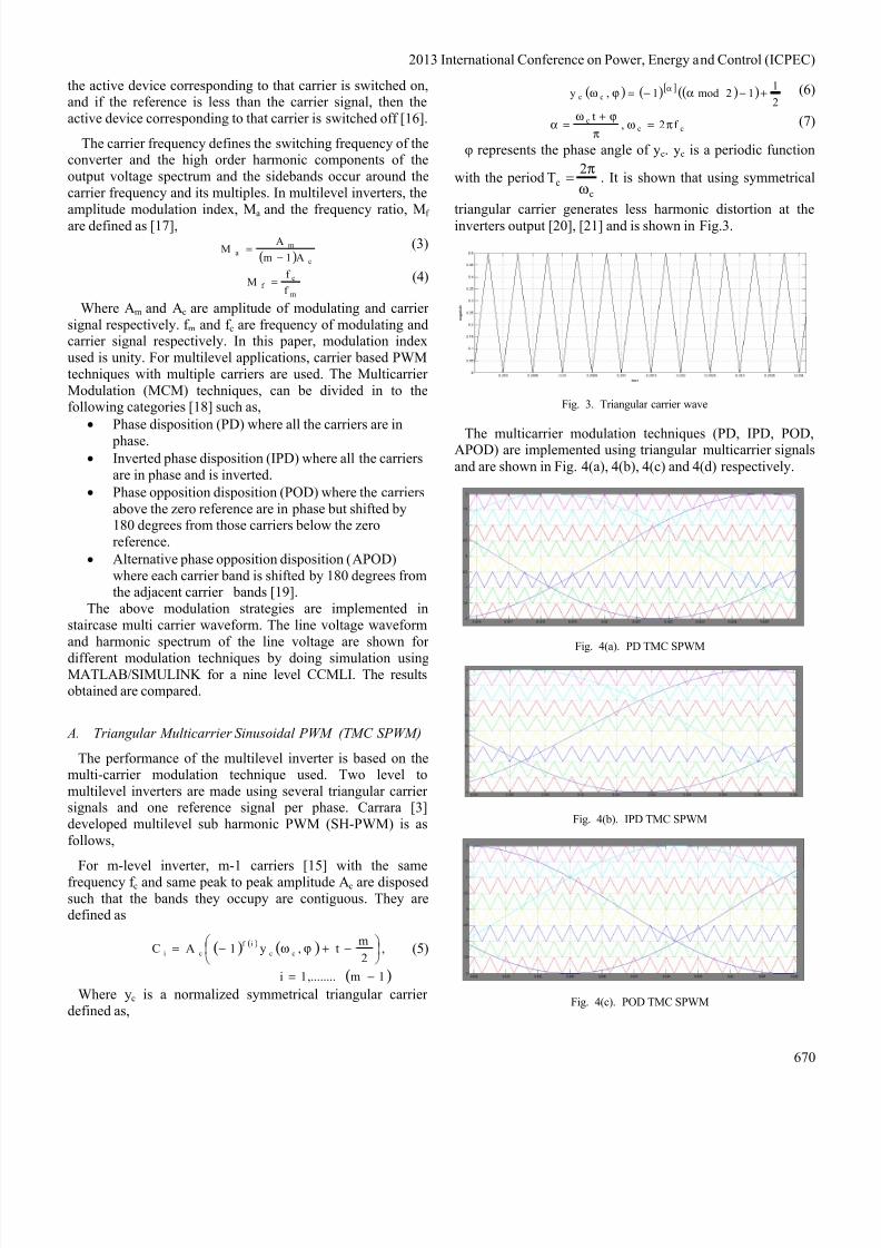
triangular carrier generates less harmonic distortion at theinverters output [20], [21] and is shown in Fig.3.
Fig. 3. Triangular carrier wave
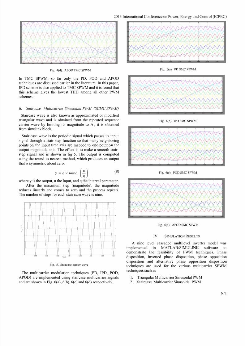
The multicarrier modulation techniques (PD, IPD, POD,APOD) are implemented using triangular multicarrier signalsand are shown in Fig. 4(a), 4(b), 4(c) and 4(d) respectively.
Fig. 4(a). PD TMC SPWM
Fig. 4(b). IPD TMC SPWM
Fig. 4(c). POD TMC SPWM
8/10/2019 Staircase Multicarrier SPWM Technique for Nine Level Cascaded Inverter
http://slidepdf.com/reader/full/staircase-multicarrier-spwm-technique-for-nine-level-cascaded-inverter 4/8
2013 International Conference on Power, Energy and Control (ICPEC)
671
Fig. 4(d). APOD TMC SPWM
In TMC SPWM, so far only the PD, POD and APODtechniques are discussed earlier in the literature. In this paper,IPD scheme is also applied to TMC SPWM and it is found thatthis scheme gives the lowest THD among all other PWMschemes.
B. Staircase Multicarrier Sinusoidal PWM (SCMC SPWM)
Staircase wave is also known as approximated or modified
triangular wave and is obtained from the repeated sequencecarrier wave by limiting its magnitude to A c, it is obtainedfrom simulink block,
Stair case wave is the periodic signal which passes its inputsignal through a stair-step function so that many neighboring
points on the input time axis are mapped to one point on theoutput magnitude axis. The effect is to make a smooth stair-step signal and is shown in fig 5. The output is computedusing the round-to-nearest method, which produces an outputthat is symmetric about zero.
×=
qu
roundqy (8)
where y is the output, u the input, and q the interval parameter.After the maximum step (magnitude), the magnitudereduces linearly and comes to zero and the process repeats.The number of steps for each stair case wave is nine.
Fig. 5. Staircase carrier wave
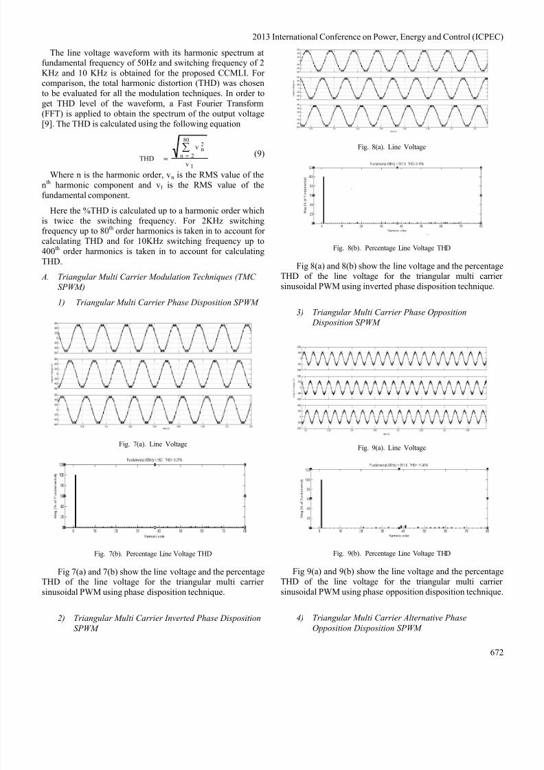
The multicarrier modulation techniques (PD, IPD, POD,APOD) are implemented using staircase multicarrier signalsand are shown in Fig. 6(a), 6(b), 6(c) and 6(d) respectively.
Fig. 6(a). PD SMC SPWM
Fig. 6(b). IPD SMC SPWM
Fig. 6(c). POD SMC SPWM
Fig. 6(d). APOD SMC SPWM
IV. SIMULATION R ESULTS
A nine level cascaded multilevel inverter model wasimplemented in MATLAB/SIMULINK software todemonstrate the feasibility of PWM techniques. Phasedisposition, inverted phase disposition, phase oppositiondisposition and alternative phase opposition dispositiontechniques are used for the various multicarrier SPWMtechniques such as
1. Triangular Multicarrier Sinusoidal PWM2. Staircase Multicarrier Sinusoidal PWM
8/10/2019 Staircase Multicarrier SPWM Technique for Nine Level Cascaded Inverter
http://slidepdf.com/reader/full/staircase-multicarrier-spwm-technique-for-nine-level-cascaded-inverter 5/8
2013 International Conference on Power, Energy and Control (ICPEC)
672
The line voltage waveform with its harmonic spectrum atfundamental frequency of 50Hz and switching frequency of 2KHz and 10 KHz is obtained for the proposed CCMLI. Forcomparison, the total harmonic distortion (THD) was chosento be evaluated for all the modulation techniques. In order toget THD level of the waveform, a Fast Fourier Transform(FFT) is applied to obtain the spectrum of the output voltage[9]. The THD is calculated using the following equation
1
80
2n
2n
v
v
THD
∑==
(9)
Where n is the harmonic order, v n is the RMS value of thenth harmonic component and v 1 is the RMS value of thefundamental component.
Here the %THD is calculated up to a harmonic order whichis twice the switching frequency. For 2KHz switchingfrequency up to 80 th order harmonics is taken in to account forcalculating THD and for 10KHz switching frequency up to400 th order harmonics is taken in to account for calculatingTHD.
A. Triangular Multi Carrier Modulation Techniques (TMCSPWM)
1) Triangular Multi Carrier Phase Disposition SPWM
Fig. 7(a). Line Voltage
Fig. 7(b). Percentage Line Voltage THD
Fig 7(a) and 7(b) show the line voltage and the percentageTHD of the line voltage for the triangular multi carriersinusoidal PWM using phase disposition technique.
2) Triangular Multi Carrier Inverted Phase DispositionSPWM
Fig. 8(a). Line Voltage
Fig. 8(b). Percentage Line Voltage THD
Fig 8(a) and 8(b) show the line voltage and the percentageTHD of the line voltage for the triangular multi carriersinusoidal PWM using inverted phase disposition technique.
3) Triangular Multi Carrier Phase Opposition Disposition SPWM
Fig. 9(a). Line Voltage
Fig. 9(b). Percentage Line Voltage THD
Fig 9(a) and 9(b) show the line voltage and the percentageTHD of the line voltage for the triangular multi carriersinusoidal PWM using phase opposition disposition technique.
4) Triangular Multi Carrier Alternative PhaseOpposition Disposition SPWM
8/10/2019 Staircase Multicarrier SPWM Technique for Nine Level Cascaded Inverter
http://slidepdf.com/reader/full/staircase-multicarrier-spwm-technique-for-nine-level-cascaded-inverter 6/8
2013 International Conference on Power, Energy and Control (ICPEC)
673
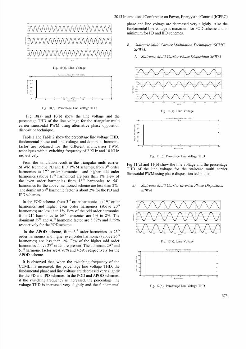
Fig. 10(a). Line Voltage
Fig. 10(b). Percentage Line Voltage THD
Fig 10(a) and 10(b) show the line voltage and the
percentage THD of the line voltage for the triangular multicarrier sinusoidal PWM using alternative phase oppositiondisposition technique.
Table.1 and Table.2 show the percentage line voltage THD,fundamental phase and line voltage, and dominant harmonicfactor are obtained for the different multicarrier PWMtechniques with a switching frequency of 2 KHz and 10 KHzrespectively.
From the simulation result in the triangular multi carrierSPWM technique PD and IPD PWM schemes, from 3 rd orderharmonics to 17 th order harmonics and higher odd orderharmonics (above 17 th harmonics) are less than 1%. Few ofthe even order harmonics from 18 th harmonics to 54 th harmonics for the above mentioned scheme are less than 2%.The dominant 57 th harmonic factor is about 2% for the PD andIPD schemes.
In the POD scheme, from 3 rd order harmonics to 19 th orderharmonics and higher even order harmonics (above 20 th harmonics) are less than 1%. Few of the odd order harmonicsfrom 21 st harmonics to 69 th harmonics are 1% to 2%. Thedominant 39 th and 41 st harmonic factor are 5.37% and 5.59%respectively for the POD scheme.
In the APOD scheme, from 3 rd order harmonics to 25 th order harmonics and higher even order harmonics (above 26 th harmonics) are less than 1%. Few of the higher odd orderharmonics above 27 th order are present. The dominant 29 th and51 st harmonic factor are 4.70% and 4.59% respectively for theAPOD scheme.
It is observed that, when the switching frequency of theCCMLI is increased, the percentage line voltage THD, thefundamental phase and line voltage are decreased very slightlyfor the PD and IPD schemes. In the POD and APOD schemes,if the switching frequency is increased, the percentage linevoltage THD is increased very slightly and the fundamental
phase and line voltage are decreased very slightly. Also thefundamental line voltage is maximum for POD scheme and isminimum for PD and IPD schemes.
B. Staircase Multi Carrier Modulation Techniques (SCMCSPWM)
1) Staircase Multi Carrier Phase Disposition SPWM
Fig. 11(a). Line Voltage
Fig. 11(b). Percentage Line Voltage THD
Fig 11(a) and 11(b) show the line voltage and the percentageTHD of the line voltage for the staircase multi carrierSinusoidal PWM using phase disposition technique.
2) Staircase Multi Carrier Inverted Phase DispositionSPWM
Fig. 12(a). Line Voltage
Fig. 12(b). Percentage Line Voltage THD

8/10/2019 Staircase Multicarrier SPWM Technique for Nine Level Cascaded Inverter
http://slidepdf.com/reader/full/staircase-multicarrier-spwm-technique-for-nine-level-cascaded-inverter 7/8
2013 International Conference on Power, Energy and Control (ICPEC)
674
Fig 12(a) and 12(b) show the line voltage and the percentageTHD of the line voltage for the staircase multi carriersinusoidal PWM using inverted phase disposition technique.
3) Staircase Multi Carrier Phase Opposition DispositionSPWM
Fig. 13(a). Line Voltage
Fig. 13(b). Percentage Line Voltage THD
Fig 13(a) and 13(b) show the line voltage and the percentageTHD of the line voltage for the staircase multi carriersinusoidal PWM using phase opposition disposition technique.
4) Staircase Multi Carrier Alternative Phase Opposition Disposition SPWM
Fig. 14(a). Line Voltage
Fig. 14(b). Percentage Line Voltage THD
Fig 14(a) and 14(b) show the line voltage and the percentageTHD of the line voltage for the staircase multi carriersinusoidal PWM using alternative phase opposition dispositiontechnique.
From the simulation result in the staircase multi carrierSPWM technique PD and IPD PWM schemes, from 3 rd orderharmonics to 31 st order harmonics are less than 1%. Few ofthe odd and even order harmonics from 32 nd harmonics to 79 th harmonics for the above mentioned scheme are less than 2%.The dominant 57 th harmonic factor is about 2% for the PD andIPD scheme.
In the POD scheme, from 3 rd order harmonics to 20 th orderharmonics and higher even order harmonics (above 20 th harmonics) are less than 1%. Few of the odd order harmonicsfrom 21 st harmonics to 79 th harmonics are 1% to 2%. Thedominant 39 th and 41 st harmonic factor are 5.60% and 5.64%respectively for the POD scheme.
In the APOD scheme, from 3 rd order harmonics to 26 th order harmonics and higher even order harmonics (above 26 th harmonics) are less than 1%. Few of the higher odd orderharmonics above 27 th order are present. The dominant 29 th and51 st harmonic factor are 4.79% and 4.68% respectively for theAPOD scheme.
It is observed that, when the switching frequency of theCCMLI is increased, the percentage line voltage THD, thefundamental phase and line voltage are decreased very slightlyfor the PD and IPD schemes. In the POD and APOD schemes,if the switching frequency is increased, the percentage linevoltage THD is increased very slightly and the fundamental
phase and line voltage are decreased very slightly. Also thefundamental line voltage is maximum for POD scheme and isminimum for PD and IPD schemes.
TABLE.ILINE VOLTAGE % THD, FUNDAMENTAL VOLTAGE PER PHASE,
FUNDAMENTAL LINE VOLTAGE AND DOMINANT HARMONIC FACTOR FOR SWITCHING FREQUENCY=2KHZ
Switching Frequency = 2KHz
ModulationTechnique
Linevoltage
% THD
Voltageer phase
(volts)
Linevoltage(volts)
Dominantharmonic
factor (%)
TriangularMulticarrier
PD 8.21 227 391.2 H57=1.83IPD 8.19 227 391.2 H 57=1.84
POD 11.45 227.1 392.8 H39=5.37H41=5.59
APOD 12.22 227 392.7 H29=4.70H51=4.59
StaircaseMulticarrier
PD 8.33 228.5 392.9 H57=1.88IPD 8.31 228.5 392.9 H 57=1.89
POD 12.08 229.7 396.5H39=5.60H41=5.64
APOD 12.49 229.2 396.4 H29=4.79H51=4.68

8/10/2019 Staircase Multicarrier SPWM Technique for Nine Level Cascaded Inverter
http://slidepdf.com/reader/full/staircase-multicarrier-spwm-technique-for-nine-level-cascaded-inverter 8/8
2013 International Conference on Power, Energy and Control (ICPEC)
675
TABLE.IILINE VOLTAGE % THD, FUNDAMENTAL VOLTAGE PER PHASE,
FUNDAMENTAL LINE VOLTAGE AND DOMINANT HARMONIC FACTOR FOR SWITCHING FREQUENCY=10KHZ
Switching Frequency = 10KHz
ModulationTechnique
Linevoltage
% THD
Voltageer phase
(volts)
Linevoltage(volts)
Dominantharmonic
factor (%)
TriangularMulticarrier
PD 8.18 226.4 389.9 H 377=1.65IPD 8.17 226.4 389.9 H 377=1.66
POD 12.49 226.7 392 H 199=6.01H201=5.99
APOD 12.71 226.9 392.1 H 189=4.85H211=4.85
StaircaseMulticarrier
PD 8.24 228.4 392.1 H 377=1.61IPD 8.23 228.4 392.1 H 377=1.62
POD 12.32 229.1 395.1 H 199=5.81H201=5.76
APOD 12.66 228.8 394.8 H 189=4.98H211=4.93
V. CONCLUSION
The simulation results for a three phase cascaded nine levelinverter which use staircase carrier wave as novel multicarrierModulation technique is obtained throughMATLAB/SIMULINK. In staircase carrier waveform,different techniques such as phase disposition (PD), inverted
phase disposition (IPD), phase opposition disposition (POD)and alternative phase opposition disposition (APOD) areimplemented. The output quantities like fundamental phaseand line voltage, percentage THD of the line voltage and
percentage dominant harmonic factor are being found. Whenthe switching frequency is 2 KHz, staircase (POD) schemegives maximum line voltage and triangular (IPD) schemegives minimum % THD for line voltage. When the switching
frequency is 10 KHz, staircase (POD) scheme gives maximumline voltage and triangular (IPD) scheme gives minimum %THD for line voltage. The proposed methods offer betterharmonic performance and selection of proper switchingfrequency in the pulse width modulation strategies enhancesthe fundamental output voltage.
R EFERENCES
[1] Mariusz Malinowski, K. Gopakumar, Jose RodriguezandMarcelo A. Pérez, “A Survey on Cascaded Multilevel Inverters”
IEEE Transactions on Industrial Electronics , vol. 57, n. 7, July2010, pp 2197 – 2206.
[2]Jang-Hwan Kim, A carrier-Based PWM Method for Three-PhaseFour-Leg Voltage Source Converters”, IEEE transactions on
ower electronics , vol. 19, n.1, January 2004. [3] G.Carrara, S.Gardella, M.Marchesoni, R.Salutari, G.Sciutto, “A
New Multilevel PWM Method: A Theoretical Analysis,” IEEETrans. Power Electronics, vol. 7, n.3 , July 1992, pp 497-505.
[4] S.M.Ayob, Z.Salam, “Trapezoidal PWM Scheme for CascadedMultilevel Inverter” First International Power and EnergyConference , November 2006, pp 368-372.
[5] Rodriguez, Jih-sheng lai, and F.Zheng peng, “MultilevelInverters; A Survey of Topologies, Controls, and Applications,”
IEEE Trans.Ind.Electron , vol.49, n. 4, pp724-738, Aug.2002.
[6] Samir koaro, PabloLezana, Mauricio Anguio and Jose Rodriguez,“Multicarrier PWM DC-Link ripple forward compensation formultilevel inverters,” IEEE Trans. Power.Electron., vol.123, n.1 ,
pp.52-56, Jan 2008.[7] Nabae, I. Takahashi, and H. Akagi, (Sep./Oct. 1981) “A new
neutral-point-clamped PWM inverter,” IEEE Trans. Ind. Appl.,vol. IA-17, n. 5, pp. 518–523.
[8] K.A.Corzine, and Y.L.Familiant, “A New Cascaded Multi-levelH-Bridge Drive,” IEEE Trans. Power Electron , vol.17, n.1 , pp.125-131, Jan 2002.
[9] R.Teodorescu,F.Blaabjerg, J.K.Pedersen, E.Cengelci, andP.N.Enjeti, “Multilevel Inverter by cascading industrial VSI,” IEEE Trans. Ind. Electron , vol.49, n.4, pp 832-838, Aug 2002.
[10] J.S.Lai, and F.Z.Peng, “Multilevel converters – A new bread ofconverters,” IEEE Trans. Ind.Appli., vol.32, n.3 , pp.509-517,May/Jun. 1996.
[11] T.A.Maynard, M.Fadel and N.Aouda, “Modelling of Multilevelconverter,” IEEE Trans. Ind.Electron., vol.44, pp 356-364,Jun.1997.
[12] P.Bhagwat, and V.R.Stefanovic, “Generalized structure of amultilevel PWM Inverter,” IEEE Trans. Ind. Appln., vol.1A-19,n.6, pp.1057-1069, Nov/Dec, 1983.
[13] Panagiotis Panagis, Fotis Stergiopoulos, Pantelis Marabeas andStefanos Manias, “Comparison of State of the Art MultilevelInverters” IEEE Trans , 2008, pp 4296-4301.
[14] Fang.Z. Peng, John W.Mckeever, and Donald J.Adams, “APower line conditioner using Cascade Multilevel Inverters forDistribution systems” IEEE Transactions on Industrial pplications, vol. 34, n.6, pp 1293-1298, Nov/Dec 1998.
[15] B.P.Mcgrath, D.G.Holmes, “Multicarrier PWM strategies formultilevel inverters,” IEEE Trans. Ind.Electron , vol 49, n.4, pp858-867,Aug.2002.
[16] Ms.T.Prathiba, Dr.P.Renuga, “Multi Carrier PWM Based MultiLevel Inverter For High Power Applications” Int. Journal ofComputer Applications , vol.1, n. 9, 2010, pp 67-71.
[17] Lion M.Tolbert and Thomas.G.Habetler, “Novel Multi LevelInverter Carrier Based PWM methods”, IEEE IAS , 1998, pp1424-1431.
[18] D.G.Holmes and T.A.Lipo, Pulse Width Modulation For PowerConverters (Wiley Inter-science, 2003).
[19] D.G.Holmes and B.P.Mcgrath, “Opportunities for harmoniccancellation with carrier based PWM for two level and multilevelcascaded inverters”, in conf.prec IEEE/IAS Annual meeting, 1999.
[20] C.Govindaraju, Dr.K.Baskaran, “Optimized Hybrid PhaseDisposition PWM control method for multilevel inverter” ACEEE Int. Journal on Electrical and Power Engineering , vol. 1, n. 1, Jan 2010, pp 36-40.
[21] J.Hamman and F.S.Van Der merwe, “Voltage harmonicsgenerated by voltage fed inverters using PWM natural sampling”
IEEE Trans. Power Electron , vol PE-3,n.3, pp.297-302, Jul.1988.