statistical analysis and optimization of asynchronous ...€¦ · statistical analysis and...
TRANSCRIPT
1
Statistical Analysis and Optimization of Asynchronous Digital Circuits
Tsung-Te Liu and Jan M. Rabaey
University of California, Berkeley
Outline
• Motivation • Variability model of CMOS digital circuit • Performance model for different timing schemes • Performance comparison • Conclusion
2
3
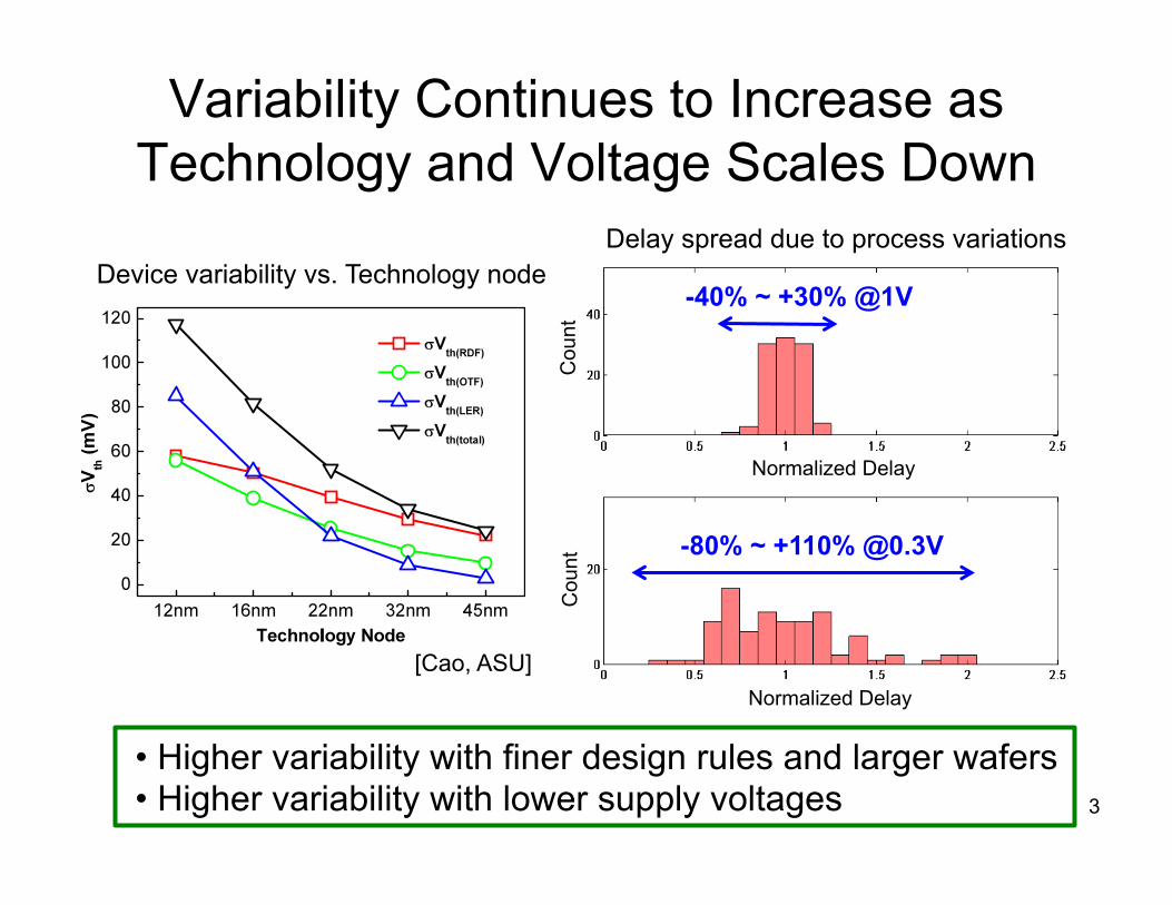
Variability Continues to Increase as Technology and Voltage Scales Down
Device variability vs. Technology node
-80% ~ +110% @0.3V
-40% ~ +30% @1V
Normalized Delay
Delay spread due to process variations
Normalized Delay
Cou
nt
Cou
nt
• Higher variability with finer design rules and larger wafers • Higher variability with lower supply voltages
[Cao, ASU]
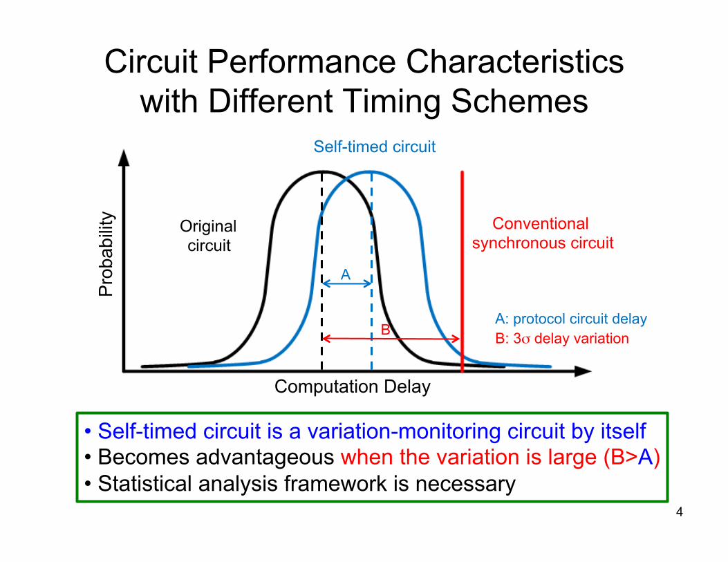
Circuit Performance Characteristics with Different Timing Schemes
Original circuit
Self-timed circuit
Conventional synchronous circuit
Computation Delay
Pro
babi
lity
• Self-timed circuit is a variation-monitoring circuit by itself • Becomes advantageous when the variation is large (B>A) • Statistical analysis framework is necessary
B: 3σ delay variation A: protocol circuit delay
A
B
4
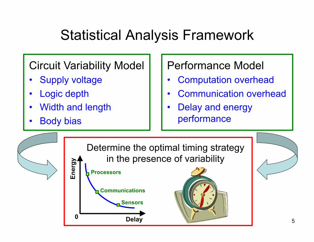
Statistical Analysis Framework
5
Circuit Variability Model • Supply voltage • Logic depth • Width and length • Body bias
Performance Model • Computation overhead • Communication overhead • Delay and energy
performance
Delay
Ener
gy
0
Processors
Communications
Sensors
Determine the optimal timing strategy in the presence of variability
Outline
• Motivation • Variability model of CMOS digital circuit • Performance model for different timing schemes • Performance comparison • Conclusion
6
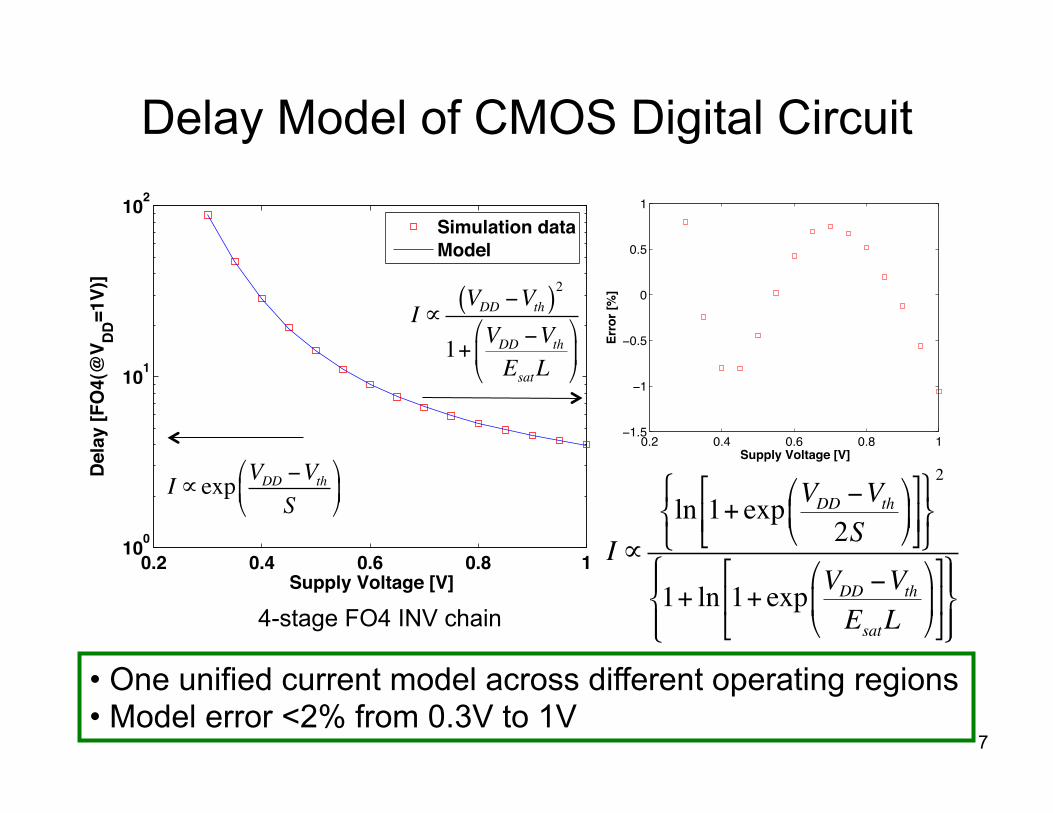
Delay Model of CMOS Digital Circuit
7
• One unified current model across different operating regions • Model error <2% from 0.3V to 1V
4-stage FO4 INV chain
0.2 0.4 0.6 0.8 1100
101
102
Supply Voltage [V]
Del
ay [F
O4(
@V DD
=1V)
]
Simulation dataModel
I !VDD "Vth( )2
1+ VDD "VthEsatL
#
$%
&
'(
I ! exp VDD "VthS
#
$%
&
'(
I !ln 1+ exp VDD "Vth
2S#
$%
&
'(
)
*+
,
-.
/01
234
2
1+ ln 1+ exp VDD "VthEsatL
#
$%
&
'(
)
*+
,
-.
/05
15
235
45
0.2 0.4 0.6 0.8 11.5
1
0.5
0
0.5
1
Supply Voltage [V]
Erro
r [%
]
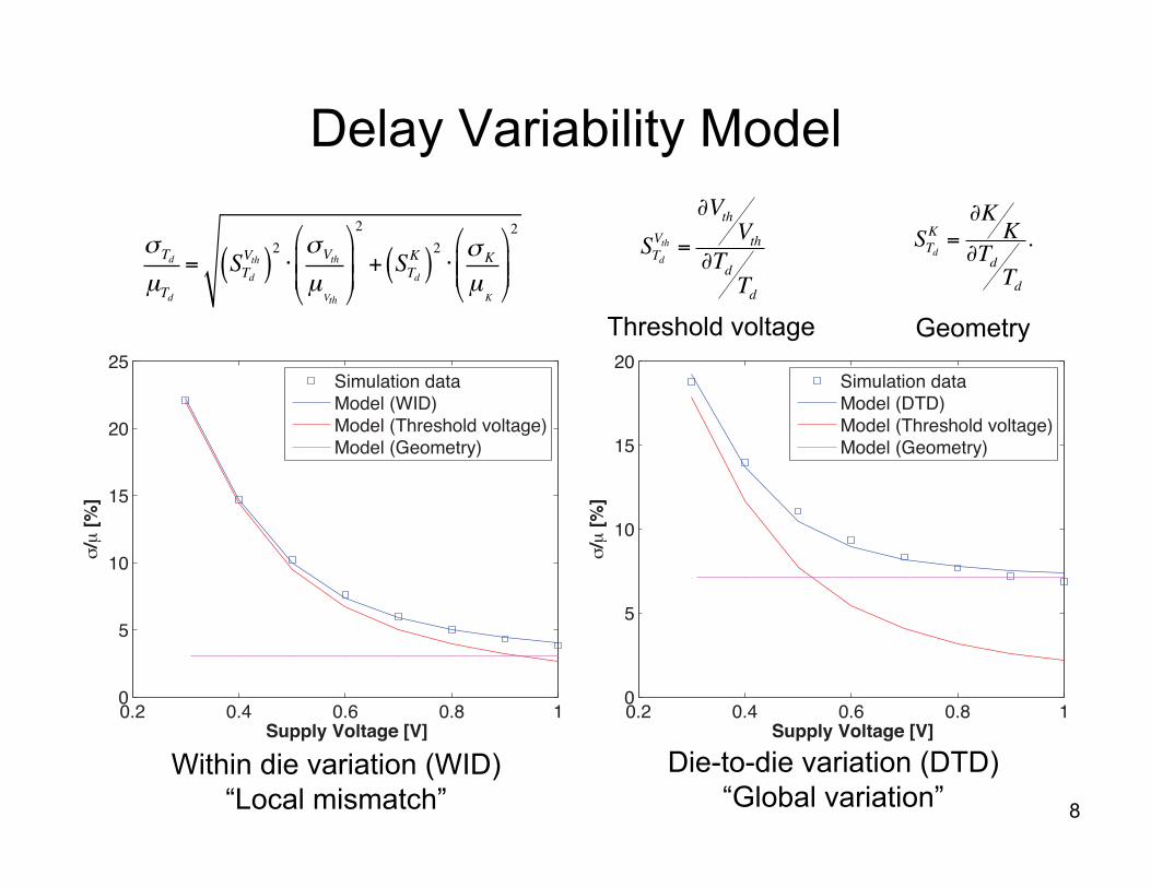
Delay Variability Model
8
Within die variation (WID) “Local mismatch”
Die-to-die variation (DTD) “Global variation”
! Td
µTd= STd
Vth( )2!!Vth
µVth
"
#$$
%
&''
2
+ STdK( )
2!! K
µK
"
#$$
%
&''
2STdVth =
!VthVth
!TdTd
0.2 0.4 0.6 0.8 10
5
10
15
20
25
Supply Voltage [V]
!/"
[%]
Simulation dataModel (WID)Model (Threshold voltage)Model (Geometry)
0.2 0.4 0.6 0.8 10
5
10
15
20
Supply Voltage [V]
!/"
[%]
Simulation dataModel (DTD)Model (Threshold voltage)Model (Geometry)
Threshold voltage Geometry
STdK =
!KK
!TdTd
.
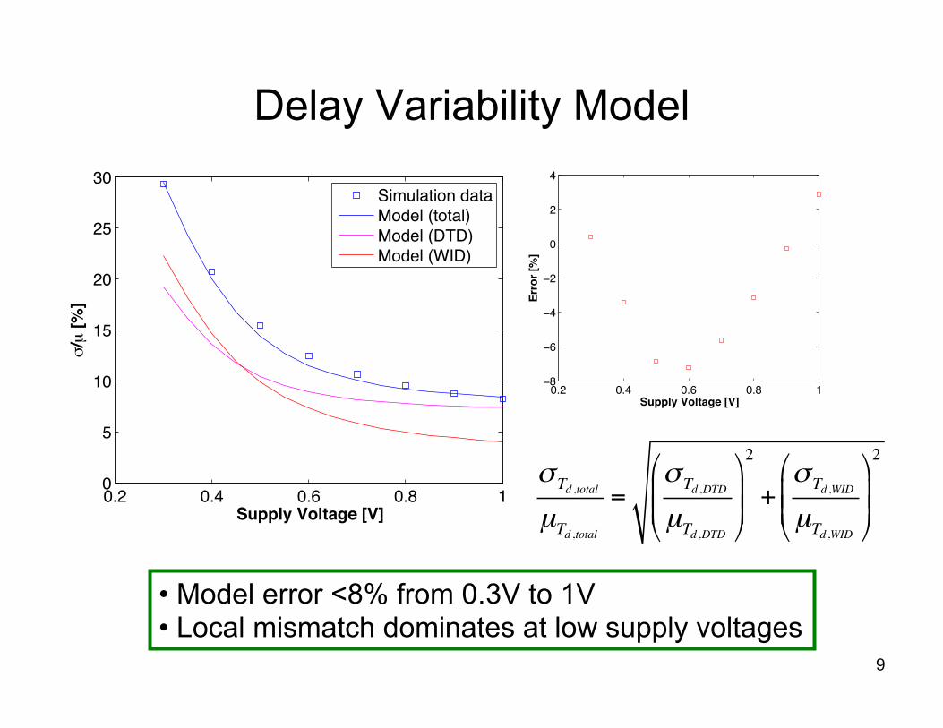
Delay Variability Model
9
0.2 0.4 0.6 0.8 10
5
10
15
20
25
30
Supply Voltage [V]
/µ [%
]
Simulation dataModel (total)Model (DTD)Model (WID)
0.2 0.4 0.6 0.8 18
6
4
2
0
2
4
Supply Voltage [V]
Erro
r [%
]
! Td ,total
µTd ,total=
! Td ,DTD
µTd ,DTD
!
"##
$
%&&
2
+! Td ,WID
µTd ,WID
!
"##
$
%&&
2
• Model error <8% from 0.3V to 1V • Local mismatch dominates at low supply voltages
0.2 0.4 0.6 0.8 15
10
15
20
25
30
Supply Voltage [V]
/µ [%
]
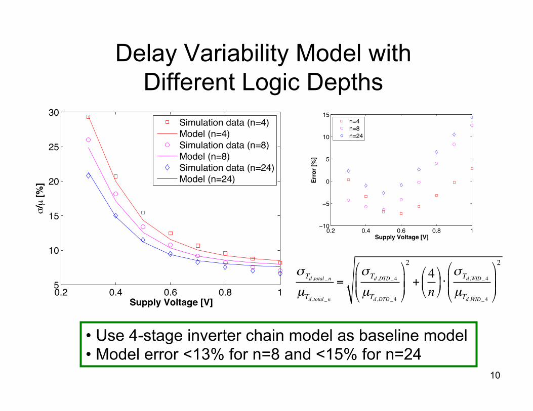
Simulation data (n=4)Model (n=4)Simulation data (n=8)Model (n=8)Simulation data (n=24)Model (n=24)
Delay Variability Model with Different Logic Depths
10
! Td ,total _n
µTd ,total _n=
! Td ,DTD_ 4
µTd ,DTD_ 4
!
"##
$
%&&
2
+4n!
"#$
%&'
! Td ,WID_ 4
µTd ,WID_ 4
!
"##
$
%&&
2
0.2 0.4 0.6 0.8 110
5
0
5
10
15
Supply Voltage [V]
Erro
r [%
]
n=4n=8n=24
• Use 4-stage inverter chain model as baseline model • Model error <13% for n=8 and <15% for n=24
Outline
• Motivation • Variability model of CMOS digital circuit • Performance model for different timing schemes • Performance comparison • Conclusion
11
Delay Overhead Evaluation
Original circuit
Dual-rail timing
Synchronous timing
Computation Delay
Pro
babi
lity
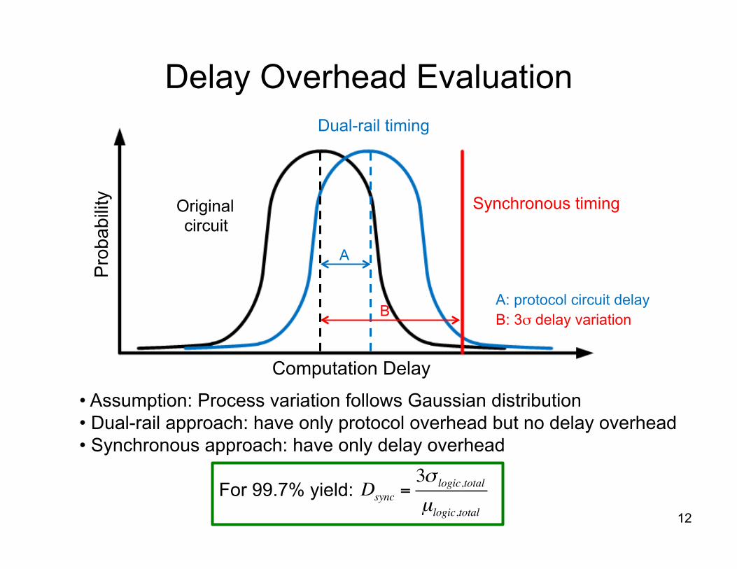
• Assumption: Process variation follows Gaussian distribution • Dual-rail approach: have only protocol overhead but no delay overhead • Synchronous approach: have only delay overhead
B: 3σ delay variation A: protocol circuit delay
A
B
12
Dsync =3! logic,total
µlogic,total
For 99.7% yield:
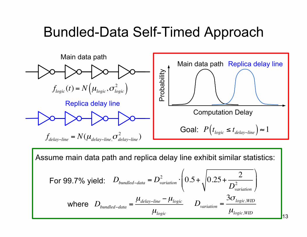
Bundled-Data Self-Timed Approach
13
Main data path
fdelay!line = N(µdelay!line,! delay!line2 )
Goal:
Assume main data path and replica delay line exhibit similar statistics:
Dbundled!data =µdelay!line !µlogic
µlogic
where
flogic (t) = N µlogic,! logic2( )
P tlogic ! tdelay"line( ) #1
Dbundled!data = Dvariation2 " 0.5+ 0.25+ 2
Dvariation2
#
$%%
&
'((
Dvariation =3! logic,WID
µlogic,WID
Replica delay line Pro
babi
lity
Computation Delay
Main data path Replica delay line
For 99.7% yield:
0 50 100 150 2000
100
200
300
400
500
600
Process Variability [%]
Del
ay O
verh
ead
[%]
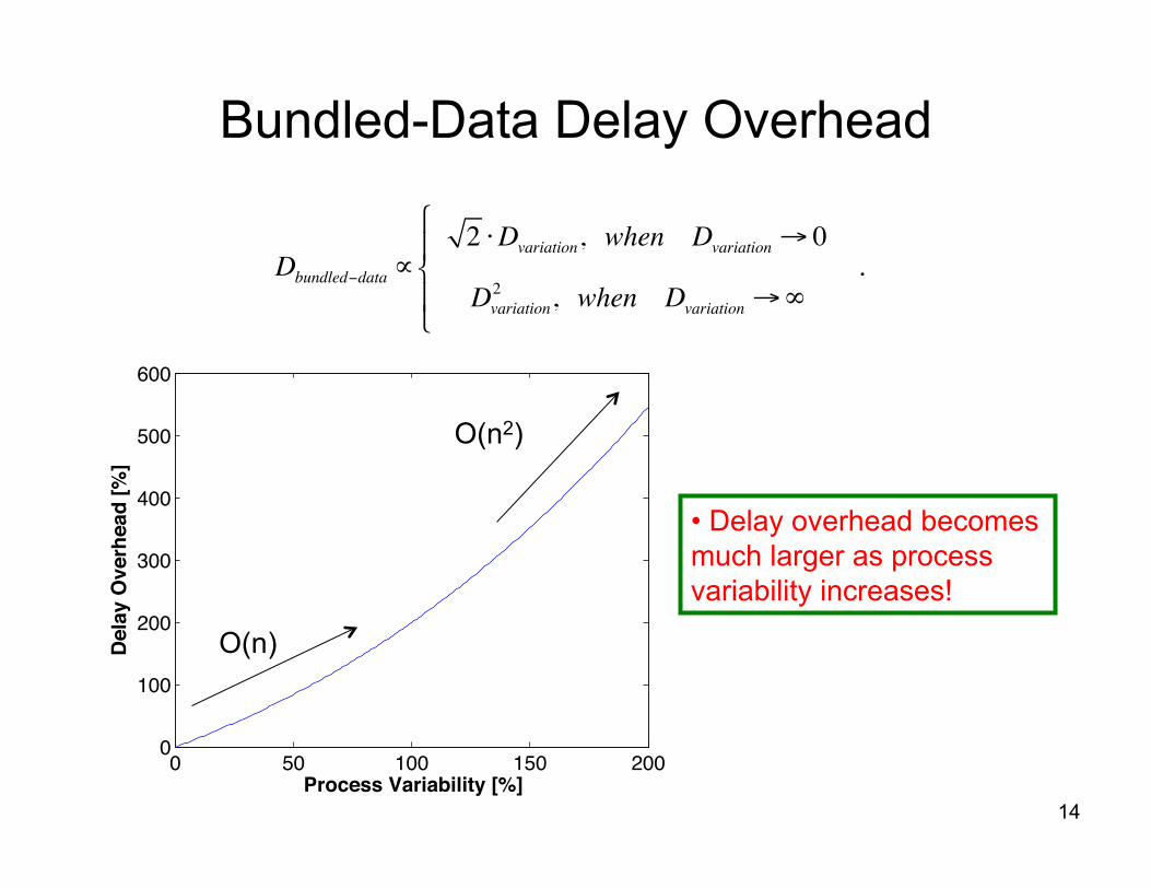
Bundled-Data Delay Overhead
14
O(n2)
O(n)
Dbundled!data "2 #Dvariation, when Dvariation $ 0
Dvariation2 , when Dvariation $%
.
&
'(
)(
• Delay overhead becomes much larger as process variability increases!
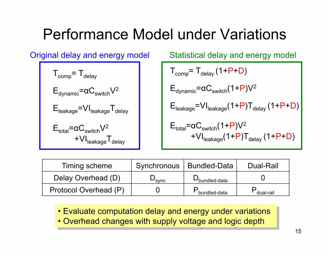
Performance Model under Variations
15
Eleakage=VIleakageTdelay
Tcomp= Tdelay (1+P+D)
Edynamic=αCswitchV2
Etotal=αCswitchV2
+VIleakageTdelay
Tcomp= Tdelay
Eleakage=VIleakage(1+P)Tdelay (1+P+D)
Edynamic=αCswitch(1+P)V2
Etotal=αCswitch(1+P)V2
+VIleakage(1+P)Tdelay (1+P+D)
Original delay and energy model Statistical delay and energy model
Timing scheme Synchronous Bundled-Data Dual-Rail Delay Overhead (D) Dsync Dbundled-data 0
Protocol Overhead (P) 0 Pbundled-data Pdual-rail
• Evaluate computation delay and energy under variations • Overhead changes with supply voltage and logic depth
Outline
• Motivation • Variability model of CMOS digital circuit • Performance model for different timing schemes • Performance comparison • Conclusion
16
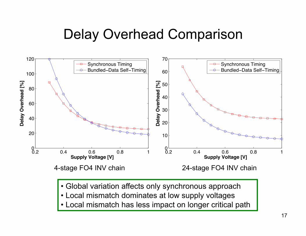
17
• Global variation affects only synchronous approach • Local mismatch dominates at low supply voltages • Local mismatch has less impact on longer critical path
4-stage FO4 INV chain
Delay Overhead Comparison
24-stage FO4 INV chain
0.2 0.4 0.6 0.8 10
20
40
60
80
100
120
Supply Voltage [V]
Del
ay O
verh
ead
[%]
Synchronous TimingBundled Data Self Timing
0.2 0.4 0.6 0.8 10
10
20
30
40
50
60
70
Supply Voltage [V]D
elay
Ove
rhea
d [%
]
Synchronous TimingBundled Data Self Timing
18
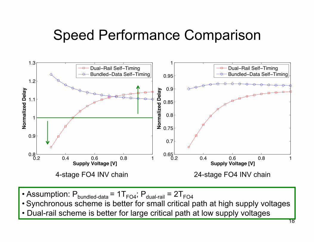
• Assumption: Pbundled-data = 1TFO4; Pdual-rail = 2TFO4 • Synchronous scheme is better for small critical path at high supply voltages • Dual-rail scheme is better for large critical path at low supply voltages
Speed Performance Comparison
4-stage FO4 INV chain 24-stage FO4 INV chain
0.2 0.4 0.6 0.8 10.8
0.9
1
1.1
1.2
1.3
Supply Voltage [V]
Nor
mal
ized
Del
ay
Dual Rail Self TimingBundled Data Self Timing
0.2 0.4 0.6 0.8 10.65
0.7
0.75
0.8
0.85
0.9
0.95
1
Supply Voltage [V]N
orm
aliz
ed D
elay
Dual Rail Self TimingBundled Data Self Timing
19
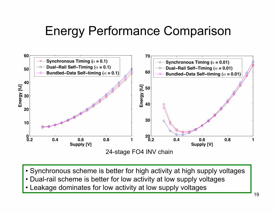
Energy Performance Comparison
24-stage FO4 INV chain
0.2 0.4 0.6 0.8 10
10
20
30
40
50
60
Supply [V]
Ener
gy [f
J]
Synchronous Timing ( = 0.1)Dual Rail Self Timing ( = 0.1)Bundled Data Self timing ( = 0.1)
0.2 0.4 0.6 0.8 120
30
40
50
60
70
Supply [V]En
ergy
[fJ]
Energy Delay Plot
Synchronous Timing ( = 0.01)Dual Rail Self Timing ( = 0.01)Bundled Data Self timing ( = 0.01)
• Synchronous scheme is better for high activity at high supply voltages • Dual-rail scheme is better for low activity at low supply voltages • Leakage dominates for low activity at low supply voltages
20
Conclusion • A statistical analysis framework is proposed to evaluate
performance of CMOS digital circuit in the presence of process variations.
• Designer can efficiently determine the optimal timing strategy, pipeline depth and supply voltage based on the proposed variability and statistical performance models.
• Asynchronous design exhibits better energy and delay characteristics for circuits with low activity and larger critical path delay under process variations
21
Acknowledgement
• Berkeley Wireless Research Center • NSF Infrastructure Grant • STMicroelectronics • Multiscale System Center
Thank you!