statistical clock skew modeling with data delay variations...statistical clock skew modeling with...
TRANSCRIPT

ld-
s.
h are
cess
ces of
ec-
d
unt
w
een
ta
est
Statistical Clock Skew Modeling with DataDelay Variations
David Harris 1 and Sam Naffziger2
[email protected], [email protected]
Abstract
Accurate clock skew budgets are important for microprocessor designers to avoid ho
time failures and to properly allocate resources when optimizing global and local path
Many published clock skew budgets neglect voltage jitter and process variation, whic
becoming dominant factors in otherwise balanced H-trees. However, worst-case pro
variation assumptions are severely pessimistic. This paper describes the major sour
clock skew in a microprocessor using a modified H-tree and applies the model to a s
ond-generation ItaniumTM Processor Family microprocessor currently under design.
Monte Carlo simulation is used to develop statistical clock skew budgets for setup an
hold time constraints in a four-level skew hierarchy. Voltage jitter through the PLL and
clock buffers accounts for the majority of skew budgets. We show that taking into acco
the number of nearly critical paths between clocked elements at each level of the ske
hierarchy and variations in the data delays of these paths reduces the difference betw
global and local skew budgets by more than a factor of two. Another insight is that da
path delay variability limits the potential cycle-time benefits of active deskew circuits
because the paths with the worst skew are unlikely to also be the paths with the long
data delays.
Keywords: clocks, clock skew, jitter, process variation, variability, noise
1. Harvey Mudd College. Claremont, CA.
2. Hewlett-Packard Corporation. Fort Collins, CO.
Statistical Clock Skew Modeling with Data Delay VariationsMarch 21, 2001 1

e per-
cess
ew
ie
k
kew
cant
val-
a sta-
gen-
aria-
n
that
ock
n
odi-
-
n-
ing a
the
I. Introduction
Clock skew is a key challenge for high-speed circuit designers because it can degrad
formance and cause chip failures. As clock frequency goes up faster than simple pro
improvement would permit, better clock distribution networks are required to keep sk
at a constant fraction of the cycle time. The problem is exacerbated by the growing d
size, clock loads, and process variability. Therefore, designers have moved from cloc
spines and ad-hoc clock routing to H-trees and grids [1]. Even when the systematic s
is completely designed away, environmental and processing variations lead to signifi
amounts of skew [2]. Assuming worst-case variations of all parameters leads to skew
ues that are large enough that design becomes impossible. Thus the designer needs
tistical model that captures the multiple independent and correlated sources of skew.
This paper develops such a statistical model for clock skew and applies it to a second
eration ItaniumTM Processor Family microprocessor currently under design. It then
describes a generalized skew budget incorporating both clock and data path delay v
tions. The model reveals several design insights. One is that considering variations i
logic delay is essential to avoid pessimistically overbudgeting global skew. Another is
jitter induced by power supply noise on the clock buffers is the dominant source of cl
skew in H-trees. A third is that the number of paths between clocked elements has a
important influence on the best clock skew budget for the design phase.
We begin in Section II by defining terms and reviewing the literature describing clock
skew budgets in high performance microprocessors. In Section III, we present the m
fied H-tree clock distribution network for the microprocessor being studied with a four
level clock skew hierarchy. We enumerate and quantify in Section IV the major enviro
mental and process variations that lead to skew in both the clock and data paths. Us
Monte Carlo simulation, we develop clock skew budgets in Section V appropriate for
setup and hold constraints at various levels of the skew hierarchy. We also examine
sensitivity of these budgets to the key parameters. Finally, we summarize the major
insights provided by the model in Section VI.
Statistical Clock Skew Modeling with Data Delay VariationsMarch 21, 2001 2

the
only
lock
ir of
ntly
ould
s
than
on
ith
w
ct to
en list
II. Background
We begin by reviewing definitions and timing constraints from the Sakallah-Mudge-
Olukotun timing analysis formulation extended to account for different clock skews
between different clock edges and different clock domains [3], [4]. In some situations
designer is primarily interested in the absolute value of skew, but in other situations,
the difference between skew in different domains. Finally, we survey the sources of c
skew and previous work budgeting skew caused by on-chip variations.
Clock skew is the difference between the nominal and actual interarrival times of a pa
clock edges [5]. We may define a hierarchy of clock domains budgeting skews differe
based on the number of shared elements in the clock distribution. For example, we c
model clocks sharing a unit-level driver as seeing only “local skew” while other clock
experience “global skew.” Clock skew is smaller for the same edge of a pair of clocks
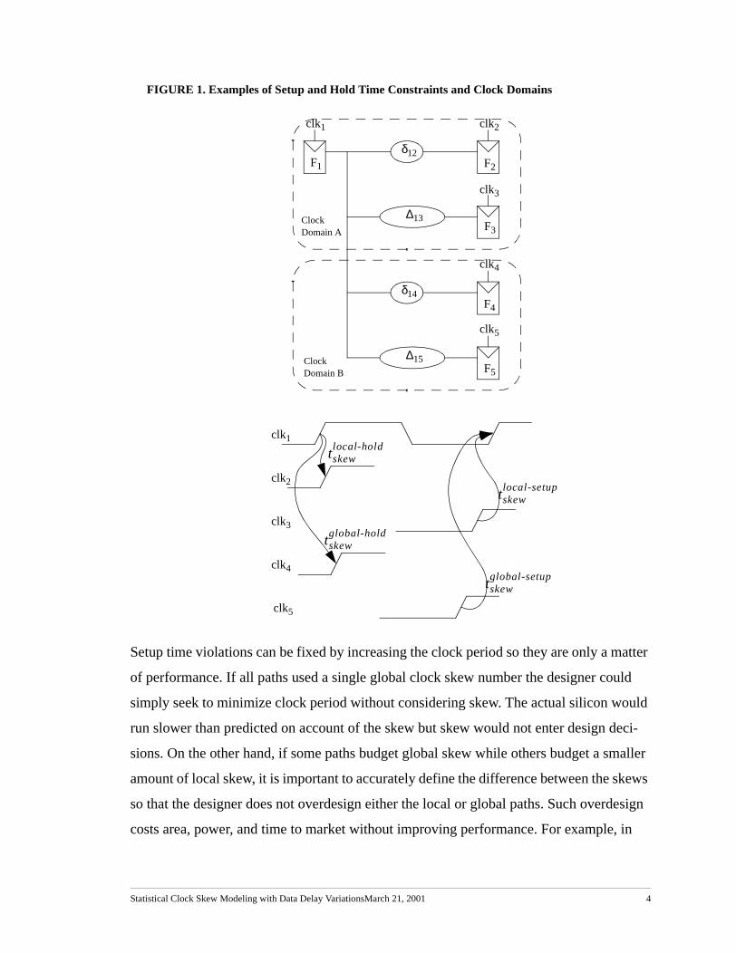
between different edges because of jitter. Figure 1 illustrates the impact of clock skew
setup and hold time constraints. All five clocks are nominally identical but are shown w
skew that could cause timing violations. Paths within a clock domain budget local ske
but paths crossing clock domains budget global skew. Hold time constraints are subje
fewer sources of skew than setup time constraints. We define system parameters, th
the timing constraints in terms of these parameters in Table 1.
• Clock cycle time, or period
• Register setup time
• Register hold time
• Maximum register clock-to-Q propagation delay
• Minimum register clock-to-Q propagation delay
• Maximum logic propagation delay from clocked elementi to j
• Minimum logic propagation delay from clocked elementi to j
TABLE 1. Timing Constraints for Figure 1
Hold Time Constraints Setup Time ConstraintsLocal ClockDomainGlobal ClockDomain
Tc
∆DC
∆CD
∆CQ
δCQ
∆ij
δij
δCQ δ12 ∆CD tskewlocal-hold+<+ ∆CQ ∆13 ∆DC+ Tc tskew
local-setup–<+
δCQ δ14 ∆CD tskewglobal-hold+<+ ∆CQ ∆15 ∆DC+ Tc tskew
global-setup–<+
Statistical Clock Skew Modeling with Data Delay VariationsMarch 21, 2001 3
atter
ld
uld
ci-
aller
ews
esign
in
FIGURE 1. Examples of Setup and Hold Time Constraints and Clock Domains
Setup time violations can be fixed by increasing the clock period so they are only a m
of performance. If all paths used a single global clock skew number the designer cou
simply seek to minimize clock period without considering skew. The actual silicon wo
run slower than predicted on account of the skew but skew would not enter design de
sions. On the other hand, if some paths budget global skew while others budget a sm
amount of local skew, it is important to accurately define the difference between the sk
so that the designer does not overdesign either the local or global paths. Such overd
costs area, power, and time to market without improving performance. For example,
∆13
clk1 clk2
clk3
clk4
clk5
∆15
ClockDomain A
ClockDomain B
δ14
δ12F1 F2
F3
F4
F5
clk1
clk2
clk3
clk4
clk5
tskewlocal-hold
tskewglobal-hold
tskewglobal-setup
tskewlocal-setup
Statistical Clock Skew Modeling with Data Delay VariationsMarch 21, 2001 4

e
iven
ers
iffer-
nt of
le for
con-
tems
er
deter-
ck
rocess
ge,
s to
tic
rce
ure 2
[6-
Figure 1, we would ideally optimize the local critical path only until it is slightly
longer than the global critical path :
(EQ 1)
Hold time violations result in nonfunctional silicon so they are much more serious. Th
cost of overbudgeting skew in hold time checks is extra delay added to short paths. G
the trade-off between nonfunctional silicon and designing in extra delay, most design
conservatively budget skew for hold time constraints.
In summary, the designer is primarily interested in the difference between skews at d
ent levels of the clock domain hierarchy for setup constraints, but the absolute amou
skew for hold constraints. The setup skew budget is subtracted from the time availab
logic to propagate from one register to the next. The hold skew budget determines the
tamination delay requirement between registers. Analogous constraints exist for sys
using latches or domino circuits. Setup time skew budgets may be further refined to
describe skew in half-cycle paths, full-cycle paths, and multi-cycle paths, but this pap
restricts itself to a single setup time skew budget for each clock domain.
Clock skew sources fall into four major categories. Systematic offsets are the skews
mined by a SPICE simulation using nominal component values. Most “zero skew” clo
papers only address the systematic offsets. Random offsets are caused by intra-die p
variations such as channel length variations. Drift, from effects like temperature chan
results in low-frequency skew changes. And jitter, especially from voltage noise, lead
high-frequency timing variation. Closed-loop clock generators can adjust for systema
and random offsets and drift but not for jitter. Hence, jitter is the most challenging sou
of skew to control.
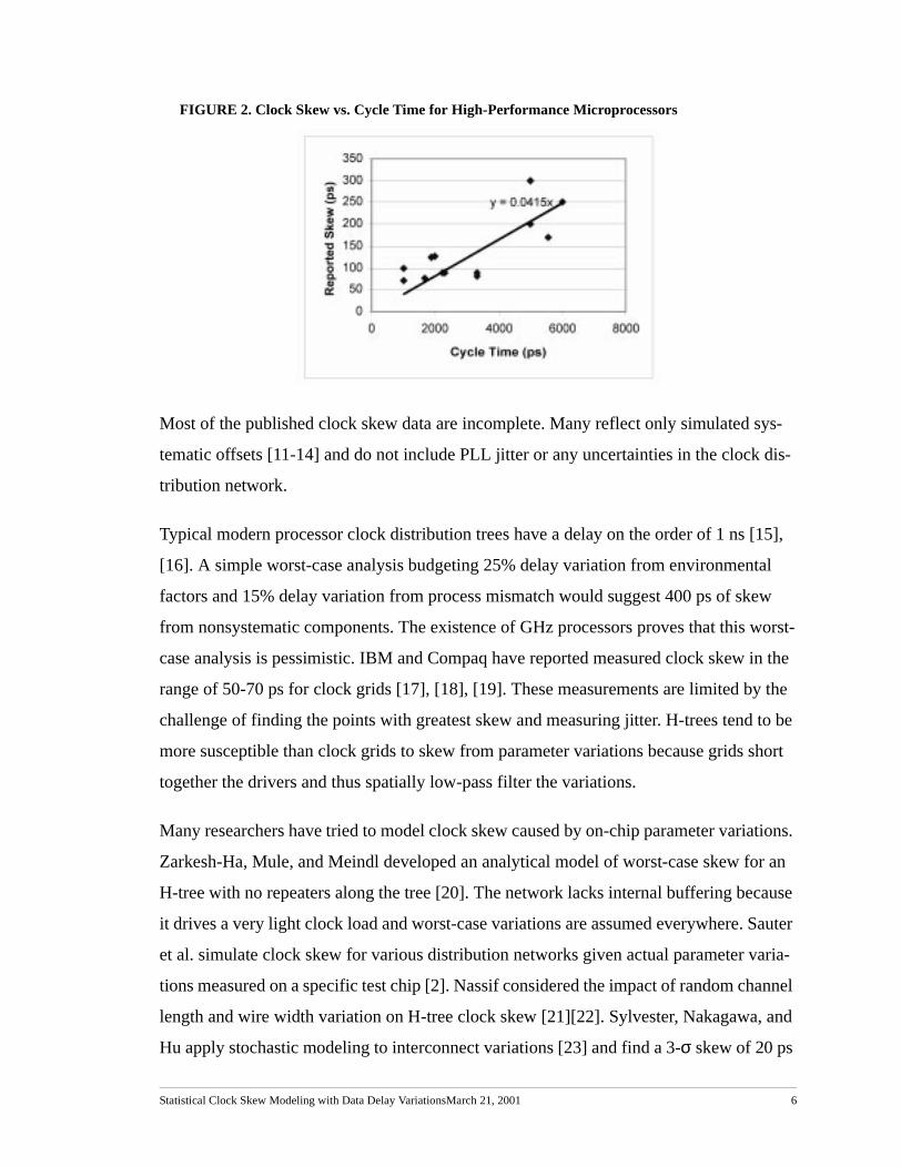
Much work has been done in the area of modeling and characterizing clock skew. Fig
illustrates published clock skews for a number of high-performance microprocessors
14] as a function of clock period. Notice that the skew budgets have typically been
reported as about 4-5% of the clock period.
∆13
∆15
∆13 ∆15 tskewglobal-setup
tskewlocal-setup–( )+=
Statistical Clock Skew Modeling with Data Delay VariationsMarch 21, 2001 5
s-
is-
5],
l
w
worst-
n the
the
o be
hort
tions.
an
ause
auter
ria-
annel
nd
FIGURE 2. Clock Skew vs. Cycle Time for High-Performance Microprocessors
Most of the published clock skew data are incomplete. Many reflect only simulated sy
tematic offsets [11-14] and do not include PLL jitter or any uncertainties in the clock d
tribution network.
Typical modern processor clock distribution trees have a delay on the order of 1 ns [1
[16]. A simple worst-case analysis budgeting 25% delay variation from environmenta
factors and 15% delay variation from process mismatch would suggest 400 ps of ske
from nonsystematic components. The existence of GHz processors proves that this
case analysis is pessimistic. IBM and Compaq have reported measured clock skew i
range of 50-70 ps for clock grids [17], [18], [19]. These measurements are limited by
challenge of finding the points with greatest skew and measuring jitter. H-trees tend t
more susceptible than clock grids to skew from parameter variations because grids s
together the drivers and thus spatially low-pass filter the variations.
Many researchers have tried to model clock skew caused by on-chip parameter varia
Zarkesh-Ha, Mule, and Meindl developed an analytical model of worst-case skew for
H-tree with no repeaters along the tree [20]. The network lacks internal buffering bec
it drives a very light clock load and worst-case variations are assumed everywhere. S
et al. simulate clock skew for various distribution networks given actual parameter va
tions measured on a specific test chip [2]. Nassif considered the impact of random ch
length and wire width variation on H-tree clock skew [21][22]. Sylvester, Nakagawa, a
Hu apply stochastic modeling to interconnect variations [23] and find a 3-σ skew of 20 ps
Statistical Clock Skew Modeling with Data Delay VariationsMarch 21, 2001 6

r
odel
m
ther
-
f
w
er-
eri-
s the
y rea-
the
t to a
lock
.
fied
dif-
five
from Monte-Carlo analysis, an improvement over a skew-corner prediction of 55 ps.
Zanella et al. [24] also describe Monte Carlo analysis, but apply it to a Viterbi Decode
with fewer than 1000 flip-flops and do not describe how their variability analysis is
derived from physical parameters. Bowman, Duvall, and Meindl have developed a m
of the impact of die-to-die and within-die parameter variations applied to the maximu
clock frequency of Pentium microprocessors [25], but focused on critical path delay ra
than clock skew.
To our knowledge, this is the first work to apply statistical models of the major compo
nents of clock skew to a high-performance microprocessor and to include the effect o
variability in data path delay. As a result, we develop a less pessimistic choice of ske
budgets for design.
III. Clock Distribution Network
We consider skew in a modified H-tree clock distribution network. An ideal H-tree is p
fectly symmetric and has zero skew from systematic mismatches, though it does exp
ence skew from random mismatches, low-frequency environmental drift, and high-
frequency voltage jitter. Unfortunately, an ideal H-tree is difficult to place within floor-
planning constraints and is unrealistic because loads are not evenly distributed acros
die.
Instead, we examine a modified H-tree where clock buffers are positioned where the
sonably fit in the floorplan. The number of buffers at each fork in the tree depends on
clock load served by the fork. Our analysis is general, but for concreteness we apply i
large microprocessor currently under development in a 0.18µm process. The clock tree
serves only the 16 x 14 mm chip core. The remainder of the die, comprising L2 cache
arrays and bus drivers with greater tolerance to clock skew, is served by an ad hoc c
distribution network offering lower power consumption at the expense of greater skew
Figure 3 shows a simplified representation of the clock network. The root of the modi
H-tree is a phase-locked loop and primary driver (PD) in the clock unit. It generates a
ferential clock which is routed on upper metal layers across 8-9 mm of interconnect to
Statistical Clock Skew Modeling with Data Delay VariationsMarch 21, 2001 7

ide
-
ed,
ck
differential repeaters. The differential signalling reduces duty cycle variation and the w
clock lines are interdigitated with supply lines to minimize inductive effects. Each
repeater drives three to seven second-level clock buffers (SLCBs) which send single
ended signals to approximately ten banks of gaters each. The gaters provide clock
enabling and clock shaping and directly drive banks of latches or dynamic logic along
short final clock lines. The modified H-tree is delay-matched rather than length-match
meaning that wire widths and lengths are tapered to provide equal delay between clo
driver stages under nominal conditions.
FIGURE 3. Clock Distribution Network and Clock Domains
PLL
Repeater
SLCB
Gater
8-9 mm
Gater Domain
SLCB Domain
Repeater Domain
PD Domain
PD
A
B
C
Statistical Clock Skew Modeling with Data Delay VariationsMarch 21, 2001 8

ne
hose
are
to
obal
get-
time
on-
o-
com-
hat
sum
even
e
cked
h is
ata
ns
ni-
pro-
The clock distribution network leads to a natural clock domain hierarchy. We can defi
skews for circuits served by the same gater, the same SLCB, the same repeater, or t
sharing only the common primary driver [26]. We will refer to these clock domains as
Gater, SLCB, Repeater, and PD, respectively. For example, all the latches in region A
in a Gater domain. Paths from A to B budget skew in the SLCB domain. Paths from A
C must budget PD domain skew. These skew domains are analogous to local and gl
clock domains in Section II but provide a finer granularity to avoid unnecessarily bud
ing excess skew. We separately define skew from rising edge to rising edge for setup
constraints and at a common edge for hold time constraints. In this study we do not c
sider skew between rising and falling edges impacted by duty-cycle variations.
This study is limited to modified H-trees. Grids can be used to reduce sensitivity to pr
cess variations at the expense of additional power [18], [1].
IV. Statistical Clock Skew Model
A worst-case clock skew model assuming maximum simultaneous variation of each
ponent of clock skew has little correlation with observed skew and is so pessimistic t
design becomes nearly impossible. An improved model takes a statistical approach to
the independent and correlated random variables that impact skew. We will see that
this model is still overly pessimistic and makes design difficult. For greatest realism w
must simultaneously consider the variations in delay through logic paths between clo
elements. Ultimately, we are interested in minimizing the expected clock period whic
limited by a combination of variations in the data and clock paths. In this section we
examine the primary sources of variation contributing to skew in both the clock and d
delays. We then describe a Monte Carlo simulation used to account for these variatio
simultaneously.
The data presented for the model is based on simulations of a second generation Ita
umTM Processor Family microprocessor clock network in the Intel 0.18µm process [27] at
low voltage (1.2V) and high temperature (110 C) assuming a 1.3 ns clock period. The
cess models are old and conservative; actual silicon is substantially faster.
Statistical Clock Skew Modeling with Data Delay VariationsMarch 21, 2001 9

ns in
han-
iso-
sub-
y
por-
150
lays
.
ints
a
rre-
wer
ring
con-
ha
ng
The
dis-
A. Clock Skew Sources
Although the clock distribution network is delay-matched to have zero nominal clock
skew up to the clock gaters, variations in processing and environment lead to variatio
delays between clocks. Each stage of clock buffer is subject to variation in effective c
nel length Le, threshold voltage Vt, operating temperature T, and supply voltage VDD.
Clock buffers are tied to the chip power supply but are heavily bypassed. The PLL is
lated from the chip supply and further bypassed to reduce jitter. Interconnect delay is
ject to variation caused by wire width and thickness variations, dielectric thickness
variation, and mismatches between relative wire and gate capacitance used for dela
matching.
The variation in delay appears as a fraction of the total delay of each stage, so it is im
tant to minimize the clock buffer delays. The PD and repeaters each have a delay of
ps. The SLCB has a delay of 280 ps. Simple gaters have a delay of 180 ps. These de
exclude wire RC flight times. The variations include:
• The power network was designed to see no more than +/- 100 mV supply variation
However, this full variation may be seen from cycle to cycle or between any two po
on the die at a given instant. Figure 4 shows the processor voltage distribution from
full-chip voltage simulation during peak switching activity. The deepest pinches co
spond to the integer execution unit and the memory I/O pads. Time-dependent po
grid collapse is discussed further in Section V.
• Full-chip power simulations in Figure 5 show a variation of 20 C across the core du
normal operation. The thermal map shows smooth variations in temperature with a
maximum gradient of 10 C between gaters served by a common SLCB. The cache
arrays along the periphery run cooler but do not contain clock buffers. This map is
sistent with thermal images of other high-performance processors such as the Alp
[6].
• Intradie Le variations come from two sources: systematic components slowly varyi
across the die and random components that apparently are spatially uncorrelated.
systematic components are specified in the process description to show a uniform
Statistical Clock Skew Modeling with Data Delay VariationsMarch 21, 2001 10

nsis-
sian
ibit
rge
2.5
olt-
ult
lay
two
tribution with half-range of 12.5 nm for transistors separated by 4 mm or more. Tra
tors in a local area see smaller variations. The random components exhibit a Gaus
distribution with a standard deviation of 3.3 nm.
• Vt variations display an inverse area dependence [28]. The threshold voltages exh
intradie variation with a standard deviation of 5% of Vt for small NMOS transistors,
4.5% for small PMOS transistors, 1.6% for large NMOS transistors, and 1.3% for la
PMOS transistors. Large transistors are defined as those with a width exceeding 1
microns. No data was available concerning about spatial correlation of threshold v
ages, so we assumed the thresholds to be spatially uncorrelated.
• Oxide thickness variations also impact transistor performance. However, it is diffic
to distinguish their effects from threshold or channel length variation. Therefore, de
variations caused by oxide thickness are lumped into the variations from the other
process parameters.
FIGURE 4. Supply Voltage Pinch During Peak Switching Activity
Statistical Clock Skew Modeling with Data Delay VariationsMarch 21, 2001 11

ds to
e
r of
evia-
ments
ove-
ub-
re
nd
e mis-
clock
s
mea-
FIGURE 5. Die Temperature Distribution during Normal Operation
Sensitivity to variations was determined from Spice simulation of clock buffers using
BSIM3 models. Voltage sensitivity is 13% delay change per 100 mV voltage change.
Temperature sensitivity is 1.5% / 20 degrees. Systematic channel length variation lea
a uniform delay distribution with a half-range of 10% of the gate delay. The cumulativ
effect of random channel length variation is negligible on account of the large numbe
transistors varying independently. Monte Carlo Spice simulation shows a standard d
tion of 2% in the delay of clock buffers caused by threshold variations.
There are several other sources of skew beyond the clock buffers. Test chip measure
show that the PLL may experience 15 ps of cycle-to-cycle jitter. This represents impr
ments in power supply filtering and process technology compared to some recently p
lished processor PLLs [29], [30]. Mismatches in the shielded, delay-matched wires a
budgeted at up to 2 ps between the PD and repeaters, 3 ps between the repeaters a
SLCBs, and 8 ps between the SLCBs and gaters. Wire process variation beyond thes
matches was considered small enough that it was not modeled. In addition, the local
wire after the gater may contribute up to 20 ps of wire RC and non-uniform gater load
may contribute up to 15 ps of delay variation. These budgets are consistent with the
Statistical Clock Skew Modeling with Data Delay VariationsMarch 21, 2001 12

lock
The
uency
up
share
sured data from [17] that indicates buffer delay variations are the dominant source of c
skew.
Table 2 summarizes which components of clock skew impact specific skew budgets.
components are categorized as systematic errors, random process variation, low-freq
drift, or high-frequency jitter. The impact of each component is listed for hold and set
checks. It is further categorized based on the clock domains it effects, i.e. paths that
the same gater, same SLCB, same repeater, or nothing but the primary driver.
TABLE 2. Impact of Skew Sources on Skew Budgets
Same Clock Edge (hold) Cycle-to-Cycle (setup)
Component Type Gater SLCB Repeater PD Gater SLCB Repeater PDPrimary Clock Driver Sources
PLL Jitter Jitter x x x x
PD V Jitter x x x x
PD T Drift
PD Le Random
PD Vt Random
Repeater Sources
PD to RepeaterWire Mismatch
Syst. x x
Repeater V Jitter x x x x x
Repeater T Drift x x
Repeater Le Random x x
Repeater Vt Random x x
Repeater Load Syst. x x
SLCB Sources
Rep. to SLCBWire Mismatch
Syst. x x x x
SLCB V Jitter x x x x x x
SLCB T Drift x x x x
SLCB Le Random x x x x
SLCB Vt Random x x x x
SLCB Load Syst. x x x x
Gater Sources
SLCB to GaterWire Mismatch
Syst. x x x x x x
Gater V Jitter x x x x x x x
Gater T Drift x x x x x x
Gater Le (global)a Random x x x x
Gater Le (local) Random x x
Gater Vt Random x x x x x x
Gater Load Syst. x x x x x x
Final Route Sources
Local wire RC Syst. x x x x x x x x
Statistical Clock Skew Modeling with Data Delay VariationsMarch 21, 2001 13

RC
r, and
ions
ari-
ation
Cycle-to-cycle skew budgets must include jitter from the entire clock distribution net-
work. All skew budgets include variations from mismatched buffer and interconnect
delay. For example, paths in the Gater domain only see mismatches in the local wire
delay after the gater. Paths in the PD domain see mismatches in repeater, SLCB, gate
local wire delays. Primary driver random process variations and drift impact all paths
equally and therefore do not contribute to skew budgets.
Table 3 summarizes the magnitude of each skew source in picoseconds. Most variat
are specified as the half-range X of a uniform distribution (+/- X). Threshold voltage v
ations are specified as a standard deviationσ of a normally distributed random variable.
The channel length variation between two nearby gates is approximately half the vari
seen across the die.
TABLE 3. Magnitude of Skew Sources (in ps)
a. Le variations are spatially correlated. Therefore, we budget less skew from gater chan-
nel length variations between two gaters that share the same SLCB and must be nearbythan from gaters using different SLCBs.
Component Half-Range SigmaPrimary Clock Driver Sources (150 ps PD delay)
PLL Jitter 7.5
PD V 19.5
Repeater Sources (150 ps repeater delay)
PD to Repeater Wire Mismatch 1
Repeater V 19.5
Repeater T 1.1
Repeater Le 15
Repeater Vt 3
Repeater Load 5
SLCB Sources (280 ps SLCB delay)
Rep. to SLCB Wire Mismatch 1.5
SLCB V 36.4
SLCB T 2.1
SLCB Le 28
SLCB Vt 5.6
SLCB Load 10
Gater Sources (180 ps gater delay)
SLCB to Gater Wire Mismatch 4
Gater V 23.4
Gater T 1.4
Gater Le (global) 18
Gater Le (local) 9
Gater Vt 3.6
Statistical Clock Skew Modeling with Data Delay VariationsMarch 21, 2001 14

f
ign to
ypical
the
lays.
t.
but
all
er
y
form
y
dget
s
on of
lock
A conservative global setup skew budget assuming worst-case / 3-sigma variations o
each parameter sums to 508 ps, about 40% of the cycle time. Clearly, we cannot des
such a conservative budget.
B. Data Skew Sources
Data paths are usually designed assuming worst-case environmental conditions but t
processing. Designers optimize paths until they meet a frequency target under these
assumptions. As a result, a chip nominally has many paths forming a “wall” just above
target frequency. However, the data delays are subject to variations just like clock de
This results in data skew and a distribution of path delays around the frequency targe
Not all data paths are designed to be exactly at the frequency target; some are close
have positive margin. Intra-die process variation results in path delay variations. Not
paths encounter worst-case environment. Tool and model inaccuracies result in furth
data skew.
We modeled data skew as the sum of three components: a uniformly distributed dela
reflecting positive margin from design and better than worst-case environment, a uni
delay from Le variations impacting all the gates in the path, and a normally distributed
delay from Vt variations.
Based on preliminary timing analysis results, we considered nearly-critical max-dela
paths to be uniformly distributed with 0 to 50 ps of slack from the 1300 ps target cycle
time. Because paths are usually more distributed than are single clock buffers, we bu
only a +/- 5% path delay variation on account of channel length variations. Simulation
show the path delay variation from threshold voltage variations has a standard deviati
0.67% of the cycle time. This is a smaller percentage variation than that of a single c
buffer because there are many more stages of gates varying independently.
Gater Load 7.5
Final Route Sources
Local wire RC 10
Component Half-Range Sigma
Statistical Clock Skew Modeling with Data Delay VariationsMarch 21, 2001 15

lus
se
gnifi-
n of
.
s the
dom
ria-
ets
lcu-
-
each
that
tially
m is
this
hich
ring
shar-
min-
ch
Similarly, we assume min-delay paths have a uniformly distributed slack of 0-30 ps p
random variations with a 30 ps standard deviation.
C. Monte Carlo Simulation
Simple RSS sums of the skew sources are not adequate to predict clock skew becau
many of the sources are not Gaussian. Moreover, the clock skew sources are only si
cant for paths which are nearly critical, and this set of paths depends on the distributio
data delays. Therefore, a Monte Carlo simulation is used to determine skew budgets
The skew sources were provided to a Monte Carlo simulation. The simulation model
clock and data paths of N chips. It randomly selects values for the systematic and ran
variations in the delay through each clock buffer and logic path. It adds worst-case va
tions from drift and jitter because these components of skew vary in time; skew budg
must be adequate for the system to operate correctly at all times. The setup skew ca
lated for each level of the clock hierarchy is the difference between the cycle time pre
dicted based on paths in that level of the hierarchy and the nominal 1.3 ns cycle time
achieved if there were no skew or data delay variations. The hold skew calculated for
level of the clock hierarchy is the amount of padding necessary to add to each path in
level of the hierarchy to ensure all paths satisfy hold time.
Using worst-case temperature drift is pessimistic because the die temperature is spa
dependent. However, the temperature variations are small enough that this pessimis
insignificant. Using worst-case voltage jitter is a more serious limitation of the model;
is addressed in Section V part C.
The Monte Carlo simulation slightly simplifies the actual clock distribution network,
assuming a single PD drives five repeaters, each of which drive six SLCBs, each of w
drive ten gaters. For setup budgets it assumes there are 500 nearly critical paths sha
only the primary driver, 100 sharing each repeater, 1000 sharing each SLCB, and 10
ing each gater. These numbers are estimated from preliminary static timing analysis
reports. For hold budgets it assumes the same number of paths are short and require
delay padding. These path counts were estimated from the chip timing database whi
Statistical Clock Skew Modeling with Data Delay VariationsMarch 21, 2001 16

d that
us
s
w. For
in-
to
so
ol
hier-
ull-
ibu-
e
, the
nated
enumerates all of the paths of concern late in the design phase. The database showe
the largest number of nearly critical paths are within individual functional units and th
share a common SLCB.
For setup constraints, we are interested in the median skew budgets over the N chip
because we bin parts and set frequency targets for typical processing and typical ske
hold constraints, we select the 95th percentile skew budget so that the yield loss to m
delay failures is low. We found N=400 was a sufficiently large number of simulations
give errors of less than 1% while consuming only a few minutes of CPU time.
V. Results
This section reports the results of the Monte Carlo skew simulations. First results are
shown without considering data delay variations. Jitter dominates the skew budgets,
numbers are also reported with and without jitter to quantify how improved jitter contr
would benefit skew. Then results are shown taking into account variations in the data
delay. This reduces the difference in skew budgets between levels of the clock skew
archy. Jitter from power supply variation is still a dominant component of skew, so a f
chip power grid simulation is used to better understand the temporal and spatial distr
tion of power supply pinch and thus avoid pessimistic jitter budgets. The modeling
involves a number of assumptions so a sensitivity analysis is performed to determine
which assumptions are most important.
A. Skew Budget without Data Delay Variations
Clock skew was first determined considering only variations in the clock paths, not th
data path. This is the conventional method of budgeting clock skew.
Table 4 lists the clock skews determined by the Monte Carlo simulation. As expected
skew increases at higher levels of the hierarchy. The skew in the setup paths is domi
Statistical Clock Skew Modeling with Data Delay VariationsMarch 21, 2001 17

itter
.
ng
-to-
en
se a
a
the
case
ew
r
y is
st
g a
there
by 213 ps of cycle-to-cycle jitter that impacts even the most local paths. Clearly, this j
caused by voltage noise in the clock buffers and PLL is the dominant source of skew
Table 5 lists the clock skews neglecting jitter. It shows the potential benefits of reduci
voltage noise. The setup skew budgets are uniformly improved by the 213 ps of cycle
cycle jitter. Local (gater) hold skew budgets had no jitter, so do not improve. The hold
skew budgets are improved for the more global paths that were subject to jitter betwe
different clock buffers. In all cases, the hold skew is larger than the setup skew becau
the budget is selected at the 95th percentile of chips rather than the median.
B. Skew Budget with Data Delay Variations
Skew budgets were then determined considering variations in both the clock and dat
paths. It is unlikely that the longest path on the chip exists between the two clocks with
worst skew. Given random data path delay variations, it is also unlikely that the worst
path is global because there are far more local paths. We determine a generalized sk
budget that describes the impact of both clock and data delay variations.
Table 6 lists the clock skews determined by the Monte Carlo simulation accounting fo
variations in the data delay as well as the clock delay. The variability in data path dela
significant for setup time calculations and on the median chip adds 75 ps to the longe
data path delay. This leads to the greatest increase in skew budgets for paths sharin
common gater which saw little clock delay variation. Similarly, it raises the setup skew
budget for paths in the SLCB domain to almost match the repeater domain because
TABLE 4. Clock Skew Budgets without Data Delay Variations (ps)
Gater SLCB Repeater PD232 267 302 312
20 106 229 280
TABLE 5. Clock Skew Budgets without Data Delay Variations or Jitter (ps)
Gater SLCB Repeater PD19 54 89 99
20 59 109 122
tskewsetup
tskewhold
tskewsetup
tskewhold
Statistical Clock Skew Modeling with Data Delay VariationsMarch 21, 2001 18
ay
4.
the
t that
ut is
er
for
ctive
e tar-
ro;
n
d to
red.
ough
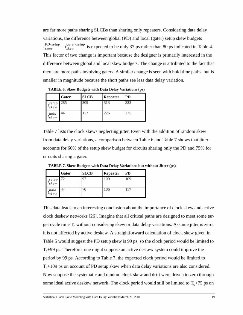
are far more paths sharing SLCBs than sharing only repeaters. Considering data del
variations, the difference between global (PD) and local (gater) setup skew budgets
is expected to be only 37 ps rather than 80 ps indicated in Table
This factor of two change is important because the designer is primarily interested in
difference between global and local skew budgets. The change is attributed to the fac
there are more paths involving gaters. A similar change is seen with hold time paths, b
smaller in magnitude because the short paths see less data delay variation.
Table 7 lists the clock skews neglecting jitter. Even with the addition of random skew
from data delay variations, a comparison between Table 6 and Table 7 shows that jitt
accounts for 66% of the setup skew budget for circuits sharing only the PD and 75%
circuits sharing a gater.
This data leads to an interesting conclusion about the importance of clock skew and a
clock deskew networks [26]. Imagine that all critical paths are designed to meet som
get cycle time Tc without considering skew or data delay variations. Assume jitter is ze
it is not affected by active deskew. A straightforward calculation of clock skew given i
Table 5 would suggest the PD setup skew is 99 ps, so the clock period would be limite
Tc+99 ps. Therefore, one might suppose an active deskew system could improve the
period by 99 ps. According to Table 7, the expected clock period would be limited to
Tc+109 ps on account of PD setup skew when data delay variations are also conside
Now suppose the systematic and random clock skew and drift were driven to zero thr
some ideal active deskew network. The clock period would still be limited to Tc+75 ps on
TABLE 6. Skew Budgets with Data Delay Variations (ps)
Gater SLCB Repeater PD285 309 313 322
44 117 226 275
TABLE 7. Skew Budgets with Data Delay Variations but without Jitter (ps)
Gater SLCB Repeater PD72 97 100 109
44 70 106 117
tskewPD-setup
tskewgater-setup–
tskewsetup
tskewhold
tskewsetup
tskewhold
Statistical Clock Skew Modeling with Data Delay VariationsMarch 21, 2001 19

time
ider-
nd
on
eth-
r sup-
ers.
st-
uiet
id
the
lied to
e
-
po-
ria-
een
he
tion.
account of the data delay variations in our model. In other words, the maximum cycle
improvement of the active deskew system is 34 ps, not 99 ps predicted without cons
ing data delay variation. This demonstrates that the interaction between data skew a
clock skew must be considered when evaluating the benefits of clock skew reduction
cycle time. Jitter reductions would be more beneficial, but active feedback deskew m
ods do not have the bandwidth to compensate for cycle-to-cycle jitter.
C. Jitter Reduction
The cycle-to-cycle jitter in the skew budgets is 213 ps because we assume that powe
ply noise of up to the +/- 100 mV design target may occur between any two clock buff
However, power supply noise exhibits both spatial and temporal locality, so such wor
case variations are unlikely to impact all clocks. Moreover, the chip tends to be most q
just before the clock edge when the SLCBs and gaters are firing. A full-chip power gr
simulation provides data to make better jitter estimates.
The full-chip power grid simulation includes models of static and dynamic logic with
appropriate power densities, the chip and package power distribution networks, and
chip and package bypass capacitance. The simulation includes a 20 A step load app
the core of the chip. Power and ground waveforms are extracted at the locations of th
clock buffers and provided to a clock network simulation that determines the cycle-to
cycle and buffer-to-buffer jitter. The power grid simulation shows both spatial and tem
ral correlations in the supply noise. In particular, the cycle-to-cycle supply voltage va
tion at a particular clock buffer is generally less than the cycle-to-cycle variation betw
two buffers.
Table 8 lists the simulated jitter figures (including a fixed 15 ps PLL setup jitter) and t
resulting skew budgets including jitter and other sources of clock and data delay varia
TABLE 8. Skew Budgets with Data Delay Variations and Simulated Jitter (ps)
Gater SLCB Repeater PD64 76 117 120
151 188 232 244
tjittersetup
tskewsetup
Statistical Clock Skew Modeling with Data Delay VariationsMarch 21, 2001 20

r those
ause
PD
s the
maller
the
the
in
ts the
s.
e the
wice
y 17
itivity
ly
We see the setup skew numbers in Table 8 represent an 80-130 ps improvement ove
of Table 6. Gater skew domains reduce jitter from the 213 ps budget to only 64 ps bec
the power supply noise impacting the clock buffers is correlated from cycle to cycle.
skew domains see less jitter improvement because the clock buffers scattered acros
chip see less correlation. Hold skew also benefits, but less so because jitter was a s
portion of the hold skew budgets.
These jitter numbers may be optimistic because it is unlikely the simulation captured
worst possible supply noise. This would be a fruitful area for further research.
D. Sensitivity Analysis
The skew budgets are based on estimates of the number of paths with low slack and
variability seen in the data delay. This section describes the sensitivity of clock skew
each level of the skew hierarchy to the estimates. In each figure, the X axis represen
clock domain and the Z axis represents the change in skew, measured in picosecond
Figure 6 shows the sensitivity to the number of short and long paths. The bars indicat
increase in skew from systems with half the estimated number of paths to those with t
the estimated number of paths. shows the greatest sensitivity, varying b
ps with changes in the assumed number of nearly critical paths. In general, the sens
is relatively low. This is important to the designer because the actual number of near
critical paths is unknown until very late in the design cycle.
0 31 93 96
44 101 199 213
TABLE 8. Skew Budgets with Data Delay Variations and Simulated Jitter (ps)
Gater SLCB Repeater PD
tjitterhold
tskewhold
tskewrepeater-setup
Statistical Clock Skew Modeling with Data Delay VariationsMarch 21, 2001 21

t,
to
aths
aths
ates
dis-
he
is is
LCB
many
FIGURE 6. Sensitivity to Number of Nearly Critical / Short Paths
Figure 7 shows the sensitivity of to the variability in critical path length. The firs
light row of bars indicates change in skew when the nearly critical paths are assume
have up to 100 ps slack, rather than up to 50 ps slack. This would account for some p
having better than worst-case supply voltage. Because there are a large number of p
this decreases the expected skews only slightly. The second, darker row of bars indic
change in skew when the nearly critical paths increase the half-range of the uniformly
tributed portion of delay variation by 10 ps. Again, with a large number of paths, it is
highly likely that one will take on nearly worst-case data skew so the overall skew
increases by 10 ps. The third, darkest row of bars indicates sensitivity to increasing t
standard deviation of the normally distributed portion of delay variations by 10 ps. Th
the most important source of variability and has the greatest impact on paths in the S
domain because it represents the greatest number of paths, one of which might see
standard deviations of variation.
Setup
Hold
Skew Sensitivity(ps)
tskewsetup
Statistical Clock Skew Modeling with Data Delay VariationsMarch 21, 2001 22

to
aths,
s. As
e
kew
FIGURE 7. Sensitivity of Setup Skew to Critical Path Variability
Figure 8 shows the sensitivity of to the variability in short path length. The first,
light row of bars indicates change in skew when the nearly short paths are assumed
have up to 60 ps of positive margin rather than 30 ps. Again, with a large number of p
this only decreases the skew budget slightly. The second, dark row of bars indicates
change in skew when the short paths increase the standard deviation in delay by 10 p
with long paths, this is the largest source of variability.
FIGURE 8. Sensitivity of Hold Skew to Short Path Variability
In all cases, the mean and median skew budgets from the Monte Carlo simulation ar
equal to within the accuracy of the simulation. The standard deviation of worst-case s
Skew Sensitivity(ps)
tskewhold
Skew Sensitivity(ps)
Statistical Clock Skew Modeling with Data Delay VariationsMarch 21, 2001 23

omain
signer
ierar-
ocal
time
de-
Such
clock
of
rs is
y also
nt in
e
the
g the
Tom
r-
ous
from chip to chip for the Gater and SLCB domains was less than 10 ps and for the
Repeater and PD domains was 10-16 ps.
VI. Conclusion
This paper has presented a set of setup and hold skew budgets in a four-level clock d
hierarchy for a microprocessor presently under design. For setup constraints, the de
is primarily concerned about the difference between skews at different levels of the h
chy, determining how much more margin must be provided for global paths than for l
paths. Poor skew budgets result in overdesign of either local or global paths. For hold
constraints, the designer is concerned about the absolute skew seen by the path. Ina
quate skew budgets result in nonfunctional silicon.
The budgets were derived from a Monte Carlo simulation of the major skew sources.
a statistical approach is important to avoid gross pessimism of summing worst-case
skew components. Simulation was necessary to model the different number of paths
between elements seeing different amounts of skew and because many components
skew exhibit a uniform rather than normal distribution.
The simulations show that jitter caused by voltage noise in the clock distribution buffe
the largest source of skew in H-trees and must be controlled as well as possible. The
show that modeling variations in data delay as well as clock network delay is importa
generating realistic skew budgets. Considering such variations reduces the differenc
between global and local skew by a factor of two. Variations in data delay also reduce
potential cycle time benefits of active deskew circuits because the paths experiencin
greatest clock skew are unlikely to be the ones with the longest data delay.
Acknowledgments
The authors would like to acknowledge the advice and data provided by Steve Wells,
Chen, Tim Michalka, and Richard McGowen. The processor design is due to the eno
mous efforts of a dedicated design team. The anonymous reviewers provided numer
helpful suggestions.
Statistical Clock Skew Modeling with Data Delay VariationsMarch 21, 2001 24

k
d
et
ro-
VII. References
[1] P. Restle and A. Deutsch, “Designing the Best Clock Distribution Network,”Proc.
VLSI Symp., pp. 2-5, June 1998.
[2] S. Sauter, D. Cousinard, R. Thewes, D. Schmitt-Landsiedel, and W. Weber, “Cloc
Skew Determination from Parametric Variations and Chip and Wafer Level,”Proc.
4th Intl. Workshop on Statistical Metrology, 1999.
[3] K. Sakallah, T. Mudge, and O. Olukotun, “Analysis and Design of Latch-Controlle
Synchronous Digital Circuits,”IEEE Trans. Computer-Aided Design, vol. 11, pp.
322-333, Mar. 1992.
[4] D. Harris, M. Horowitz, and D. Liu, “Timing Analysis Including Clock Skew,”IEEE
Trans. Computer-Aided Design, vol. 18, no. 11, Nov. 1999.
[5] D. Harris,Skew-Tolerant Domino Circuits, San Francisco, CA: Morgan Kaufmann,
2001.
[6] P. Gronowski, et al., “High Performance Microprocessor Design,”IEEE J. Solid-State
Circuits, vol. 33, no. 5, pp. 676-686, May 1998.
[7] K. Nowka and T. Galambos, “Circuit Design Techniques for a Gigahertz Integer
Microprocessor,” inProc. Intl. Conf. Comp. Design, pp. 11-16, Oct. 1998.
[8] S. Healey et al., “A 7th-Generation x86 Microprocessor,”ISSCC Dig. Tech. Papers,
pp. 92-93, Feb. 1999.
[9] J. Alvarez, et al., “450 MHz PowerPC Microprocessor with Enhanced Instruction S
and Copper Interconnect,”ISSCC Dig. Tech. Papers, pp. 96-97, Feb. 1999.
[10] R. Colwell and R. Steck, “A 0.6µm BiCMOS Processor with Dynamic Execution,”
ISSCC Dig. Tech. Papers, pp. 176-177, Feb. 1995.
[11] S. Santhanam, et al., “A Low-Cost, 300-MHz, RISC CPU with Attached Media P
cessor,”IEEE J. Solid-State Circuits, vol. 33, no. 11, Nov. 1998.
Statistical Clock Skew Modeling with Data Delay VariationsMarch 21, 2001 25

r
n-
ha
tri-
[12] N. Vasseghi, K. Yeager, E. Sarto, and M. Seddighnezhad, “200 MHz Superscala
RISC Microprocessor,”IEEE J. Solid-State Circuits, vol. 31, no. 11, pp. 1675-1686,
Nov. 1996.
[13] N. Gaddis and J. Lotz, “A 64-b Quad-Issue CMOS RISC Microprocessor,”IEEE J.
Solid-State Circuits, vol. 31, no. 11, pp. 1697-1702, Nov. 1996.
[14] C. Maier et al., “A 533-MHz BiCMOS Superscalar RISC Microprocessor,”IEEE J.
Solid-State Circuits, vol. 32, no. 11, pp. 1625-1634, Nov. 1997.
[15] P. Restle, K. Jenkins, A. Deutsch, and P. Cook, “Measurement and Modeling of O
Chip Transmission Line Effects in a 400 MHz Microprocessor,”IEEE J. Solid-State
Circuits, vol. 33, no. 4, pp. 662-665, April 1998.
[16] C. Nicoletta, et al., “A 450-MHz RISC Microprocessor with Enhanced Instruction
Set and Copper Interconnect,”IEEE J. Solid-State Circuits, vol. 34, no. 11, pp. 1478-
1491, Nov. 1999.
[17] P. Restle, et al., “A Clock Distribution Network for Microprocessors,”VLSI Symp.
Dig. Tech. Papers, pp. 184-187, June 2000.
[18] D. Bailey and B. Benschneider, “Clocking Design and Analysis for a 600-MHz Alp
Microprocessor,”IEEE J. Solid-State Circuits, vol. 33, no. 11, pp. 1627-1633, Nov.
1998.
[19] P. Sanda, et al., “Picosecond Imaging Circuit Analysis of the POWER3 Clock Dis
bution,” ISSCC Dig. Tech. Papers, pp. 372-373, Feb. 1999.
[20] P. Zarkesh-Ha, T. Mule, and J. Meindl, “Characterization and Modeling of Clock
Skew with Process Variations,”Custom Integrated Circuits Conf., pp. 441-444, 1999.
[21] S. Nassif, “Within-Chip Variability Analysis,”Intl. Elec. Device Meeting, pp. 283-
286, 1998.
[22] A. Chandrakasan, W. Bowhill, and F. Fox, ed.,Design of High-Performance Micro-
processor Circuits, Ch. 6, pp. 98-115, New York: IEEE Press, 2001.
Statistical Clock Skew Modeling with Data Delay VariationsMarch 21, 2001 26

ss
e
-
d
is-
s-
,”
[23] D. Sylvester, O. Nakagawa, and C. Hu, “Modeling the Impact of Back-End Proce
Variations on Circuit Performance,”VLSI Symp. Dig. Tech. Papers, pp. 58-61, June
1999.
[24] S. Zanella, A. Nardi, M. Quarantelli, A. Neviani, and C. Guardiani, “Analysis of th
Impact of Intra-Die Variance on Clock Skew,”Proc. 4th Intl. Workshop on Statistical
Metrology, 1999.
[25] K. Bowman, S. Duvall, and J. Meindl, “Impact of Die-to-Die and Within-Die Param
eter Fluctuations on the Maximum Clock Frequency Distribution,”ISSCC Dig. Tech.
Papers, 17.6, Feb. 2001.
[26] S. Tam, S. Rusu, U. Desai, R. Kim, J. Zhang, and I. Young, “Clock Generation an
Distribution for the First IA-64 Microprocessor,”IEEE J. Solid-State Circuits, vol.
35, no. 11, pp. 1545-1552, Nov. 2000.
[27] S. Yant, et al., “A High Performance 180 nm Generation Logic Technology,”Intl.
Elect. Dev. Meeting, pp. 8.1.1-8.1.4, 1998.
[28] M. Pelgrom, A. Duinmaijer, and A. Welbers, “Matching Properties of MOS Trans
tors,” IEEE J. Solid-State Circuits, vol. 24, no. 5, Oct. 1989.
[29] R. Heald, et al., “Implementation of a 3rd-Generation SPARC V9 64b Microproce
sor,” ISSCC Dig. Tech. Papers, pp. 412-413, Feb. 2000.
[30] J. Silberman, et al., “A 1.0-GHz Single-Issue 64-Bit PowerPC Integer Processor
IEEE J. Solid-State Circuits, vol. 33, no. 11, Nov. 1998.
Statistical Clock Skew Modeling with Data Delay VariationsMarch 21, 2001 27