statistical variability and reliability in nanoscale...
TRANSCRIPT
Statistical Variability and Reliability in Nanoscale FinFETs
Xingsheng Wang1*, Andrew R. Brown1, Binjie Cheng1 and Asen Asenov1,2
1 Device Modelling Group, School of Engineering, University of Glasgow, Glasgow G12 8LT, UK 2 Gold Standard Simulations Ltd., Rankine Building, Glasgow G12 8LT, UK
Tel: +44 (0) 141 330 2964, * E-mail: [email protected]
Abstract
A comprehensive full-scale 3D simulation study of statistical variability and reliability in emerging, scaled FinFETs on SOI substrate with gate-lengths of 20nm, 14nm and 10nm and low channel doping is presented. Excellent electrostatic integrity and resulting tolerance to low channel doping are perceived as the main FinFET advantages, resulting in a dramatic reduction of statistical variability due to random discrete dopants (RDD). It is found that line edge roughness (LER), metal gate granularity (MGG) and interface trapped charges (ITC) dominate the parameter fluctuations with different distribution features, while RDD may result in relatively rare but significant changes in the device characteristics.
I Introduction
The statistical variability and reliability introduced by RDD, LER, MGG, and random ITC in nanoscale MOSFETs is becoming one of the major concerns for CMOS scaling and integration [1][2]. The 3D FinFET architecture, adopted by Intel in the upcoming 22nm generation, which tolerates low channel doping is, in part, a response to the requirement for reducing the statistical variability in nanoscale transistors [3][4]. This paper presents a comprehensive study of the statistical variability and reliability in scaled FinFETs featuring all relevant variability sources.
II Devices and Simulation Methodology
The structure of the simulated FinFETs, fabricated on a SOI substrate, is schematically illustrated in Fig.1. Relatively thin buried oxide (BOX) and high substrate doping are chosen to decouple drain-induced fringing fields and achieve optimal electrostatic integrity and short-channel effects [5]. The device parameters listed in Table 1 follow the ITRS 2010 recommendations, with slightly more conservative scaling of EOT and supply voltage. The design of the nominal devices with stress enhancement demonstrates excellent electrostatics and short channel effects (SCE) while achieving the desirable drive currents. The GSS ‘atomistic’ simulator GARAND is employed to investigate the statistical variability and reliability [6], illustrated by an example in Fig. 2. Variability sources including random discrete dopants (RDD), gate edge roughness (GER), fin edge roughness (FER), metal gate granularity (MGG), and interface trapped charge (ITC) are simulated, individually and in combination. The random
dopants are introduced based on the nominal local doping concentration. LER is obtained from Fourier synthesis with Gaussian autocorrelation, parameterised by correlation length (30nm) and root mean square (RMS) varied in the simulations [7]. TiN gate metal grains are assumed to have two different possible crystalline orientations with different workfunctions spanning 0.2V and having 40% and 60% probability of occurrence [1]. Ensembles of 1000 devices are used to minimise statistical error.
III Statistical Variability
Full electrical transfer characteristics are simulated and the corresponding figures of merit are extracted and analysed. A combined variability case is demonstrated in Fig. 3 for a 10nm gate-length FinFET, illustrating the variation in transfer characteristics compared to the nominal design. The distributions of threshold-voltage (VT) in the three FinFET designs show that the overall VT variability is dramatically reduced compared to planar bulk MOSFETs [1][2], but the new variability source, fin-edge roughness, contributes considerable variability. Another dominant source is MGG, while RDD effects are significantly supressed (Fig. 4) due to the lack of channel doping. The VT spread increases with the gate area reduction for the scaled FinFET.
The normal Q-Q test on the VT distribution due to RDD in Fig. 5(a) shows that it closely follows a Gaussian distribution. The additional simulations show that source/ drain resistance variation due to doping fluctuations dominates the RDD variability due to the absence of channel doping. However, a single dopant rarely but possibly located in the channel can dramatically reshape the distribution tails. Observed in two extreme cases of the 14nm FinFET in Fig. 5(b), one donor in the channel can pull down the left tail of the distribution and one accepter can elevate the right tail. The LER effects are shown in Figures 6 and 7. Compared to that due to FER, GER produces a skewed VT distribution with a prolonged left tail, especially in the 10nm FinFET due to stronger SCE. However, for thin fin width, the FER can also produce a skewed distribution. Different asymmetrical sensitivity of VT to the changes in gate-length and fin-width, as shown in Fig. 8, is the reason for the observed behaviour. In addition, the threshold-voltage is more sensitive to fin-width variation compared to gate-length, causing larger FER variability than GER. The asymmetrical distribution in 10nm FinFETs due to FER is caused by the dramatically reduced current density inside the channel due to quantum

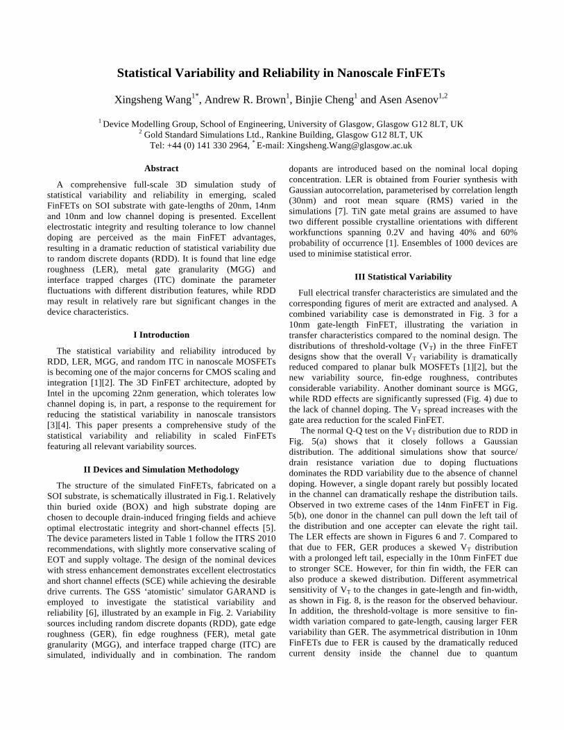
confinement, demonstrated in Fig. 9. TiN MGG can cause a bounded, dual-peaked VT distribution (Fig. 10) when metal-grain size is comparable to gate dimensions although it approximates to a Gaussian distribution with small metal grain sizes, as shown in Fig. 11. In general, the VT variability increases with the reduction in size of FinFETs while the MGG and FER are dominant sources in all three FinFETs (Fig. 12). The standard deviation of threshold-voltage can reach up to 31.5mV, 41.5mV and 51.3mV for 20nm, 14nm and 10nm gate-length FinFETs with all variability sources combined. This overall variation of device performance depends on the variability-source parameters. From Fig. 13
σVT is linearly proportional to the RMS (Δ) of the LER. Combined with the observations from Fig.8, LER-induced variability is proportional to LER magnitude and sensitivity. However, similar to MGG in bulk transistors, the linear proportionality does not hold true with large metal grains.
The on-current (ION) variation has different distribution features in Fig. 14. FER introduces the largest ION variability since FER does not just affect the channel but also the source/drain resistances, while RDD together with MGG also contribute considerably. Meanwhile MGG has the strongest correlation between ION and VT variations, but the ION with combined sources stays less correlated with VT, which means ION is also statistically important (Table 2). The drain-induced barrier lowering (DIBL) correlations with VT due to two dominant variability sources, FER and MGG, are different (Fig. 15). The DIBL has strong negative correlations with both linear and saturation threshold voltages in the presence of FER, since fin-width thinning can lead to higher threshold-voltage (both for saturation and linear) and better short-channel effects. In the presence of MGG, the drain field lowers the drain-end channel barrier, which is subject to surface potential variation, and therefore DIBL exhibits large variation.
IV Statistical Reliability
Random trapped charges at the gate oxide/fin interface in FinFETs subjected to NBTI/PBTI degradation demonstrate the statistical aspect of reliability. As an example showing trapped charges in the 3D FinFET in Fig. 16(a), traps can significantly reduce the current nearby, and even block the current in the thin fin when two or more traps are coincidentally located on opposite sides, as demonstrated in Fig. 16(b). The electron and current distributions inside the fin, due to the confining oxide barrier on all four sides, are centralised away from the interfaces. A fixed interface trap charge locally lowers the electrostatic potential, reducing the electron density nearby, further confining the carriers in the channel. Fig. 17 shows the distribution of VT-shift due to extra traps. For any given device, VT increases with a magnitude depending on the number and location of the
trapped charges. With nominal trap density 1×1011 cm-2 in the 20nm FinFET there is, on average, only one trapped charge, which can lead to VT random telegraph signal (RTS) of
several millivolts. However, a large VT-shift in the distribution tail is observed, demonstrating that multi-trapping RTS occurs [8]. A simple model, , assumes that interface charges (and/or oxide charges close to the oxide/fin interface) cause a flat-band voltage change. Due to multi-gate control the average VT shift is less than the modelled shift (Fig. 18). The average shift is linearly proportional to the average trap density as expected, but the magnitude is reduced because of the fringe capacitance. The location of individual traps, for the same number of traps, can affect the overall VT variability (Fig 19). This variation is especially prominent if the number of traps is around the
average. Combining two facts from Fig. 18 and 19, σVT more
or less follows the modelled qtox N it (εox WL ) assuming
the number of traps follows a Poisson distribution [9] in Fig. 20.
V Conclusions
Full-scale statistical simulation and analysis of intrinsic parameter fluctuation in 3D FinFETs is presented. FER and MGG are dominant VT variability sources in nanoscale FinFETs while LER may skew the variability, and FER could lead to the largest drive-current variability. Other figures of merit and their correlations are analysed together. ITC can considerably shift the characteristics, introducing an additional statistical aspect of threshold-voltage reliability.
Acknowledgements
This work is partially supported by the EU ENIAC MODERN project and EU FP7 TRAMS project.
References [1] X. Wang, A. R. Brown, N. M. Idris, S. Markov, G. Roy and A. Asenov,
“Statistical threshold-voltage variability in scaled decananometer bulk HKMG MOSFETs: a full-scale 3-D simulation scaling study,” IEEE Trans. on Elec. Dev., Vol. 58, No. 8, pp. 2293–2301, Aug. 2011.
[2] K. J. Kuhn, et al., “Process technology variation,” IEEE Trans. on Elec. Dev., Vol. 58, No. 8, pp. 2197–2208, Aug. 2011.
[3] E. Baravelli, A. Dixit, R. Rooyackers, M. Jurczak, N. Speciale, and K.D. Meyer, “Impact of line-edge roughness on FinFET matching performance,” IEEE Trans. on Elec. Dev., Vol. 54, No. 9, pp. 2466–2474, Sept. 2007.
[4] S. O’uchi, et al., “Characterization of metal-gate FinFET variability based on measurements and compact model analysis,” in IEDM Tech. Dig., 2008.
[5] T. Ernst, C. Tinella, C. Raynaud, S. Cristoloveanu, “Fringing fields in sub-0.1 μm fully depleted SOI MOSFETs: optimization of the device architecture,” Solid-State Electronics, Vol.46, pp.373-378, 2002.
[6] [online], www.GoldStandardSimulations.com [7] A. Asenov, S. Kaya, and A. R. Brown, “Intrinsic parameter fluctuations
in decananometer MOSFETs introduced by gate line edge roughness,” IEEE Trans. on Elec. Dev., Vol. 50, No. 5, pp. 1254–1260, May 2003.
[8] N. Tega, et al., “Anomalously large threshold voltage fluctuation by complex random telegraph signal in floating gate flash memory,” in IEDM Tech. Dig., 2006.
[9] A. R. Brown, V. Huard, and A. Asenov, “Statistical simulation of progressive NBTI degradation in a 45-nm technology pMOSFET,” IEEE Trans. on Elec. Dev., Vol. 57, No. 9, pp. 2320–2323, Sept. 2010.

Fig. 1: The schematic view of the 3D SOI FinFET in this study. BOX is 20nm thick, and substrate doping is 5×1018cm-2.
Table 1: The FinFET parameters
Node (nm) 22 16 11
Lg (nm) 20 14 10
EOT (nm) 0.83 0.7 0.585
Wfin (nm) 10 7 5
Hfin (nm) 25 17.5 12.5
Nsd (cm-3) 3E20 3E20 3E20
Nch (cm-3) 1E15 1E15 1E15
Vdd (V) 1 0.9 0.8
Ioff (nA/μm) 97 97 97
Idsat (μA/μm) 1411 1719 1958
SS (mV/dec) 76.8 75.1 73.2
DIBL (mV/V) 46.7 46.8 47.0
Fig. 2: Full-scale 3D statistical simulations of FinFETs, showing the electron density in the fin and potential on the gate. It is easily seen that doping fluctuations, fin-edge and gate-edge roughness, and gate workfunction fluctuation are occurring in concert.
Fig. 3: Full electrical transfer characteristics simulation of 10nm gate-length FinFETs, including random discrete dopants (RDD), gate edge roughness (GER) with 3Δ=2nm, fin edge roughness (FER) with 3Δ=2nm, and metal gate granularity (MGG) with average grain diameter of 5nm.
Fig. 4: The distributions of threshold-voltages (VT) due to different variability sources in three generations of FinFETs with gate lengths of 20nm (left), 14nm (middle) and 10nm (right).
(a)
(b) Fig. 5: (a) The normal Q-Q test on VT distributions due to RDD in 3 FinFETs. (b) Two rare extreme cases at the ends of the distribution tails of the 14nm FinFET with a single dopant in the channel.
Fig. 6: The Q-Q test on VT distribution due to gate-edge roughness. It is seen that the smaller FinFET has more strongly skewed tails. It shows that GER causes a prolonged left tail in the VT distribution.
Fig. 8: The sat. VT dependence on fin-width and gate-length for the 10nm device. It is found that the sensitivities to these two geometrical parameters are different on both sides
Fig. 7: The Q-Q test on VT distribution due to fin-edge roughness. The distribution of 10nm FinFET deviates from the normal distribution on the right side.
Fig. 9: The current density inside the channel of the 10nm gate-length FinFET with fin width of 5nm, 4nm, 3nm and 2nm. Vd=0.05V, Vg=0.2V.
LG
OXIDE
SUBSTRATE
Wfin
SOURCE
GATE
DRAIN
tox
Hfin
0 0.2 0.4 0.6 0.8V
G (V)
10-10
10-8
10-6
10-4
10-2
I D (
A/μ
m)
’Atomistic’ SamplesNominal Device
VD
=0.8V
RDDGER2FER2MGG5
00.20.40.6
00.10.2
0
0.1
00.05
0.1
Prob
abili
ty
0
0.05
0
0.05
0.05 0.1 0.15 0.2 0.25V
T (V)
0
0.05
RDD
GER (3 =2nm)
FER (3 =2nm)
Combined (MGG5)
MGG (5nm)
MGG (10nm)
Combined (MGG10)
=21.0mV
=31.5mV
00.20.40.6
0
0.1
0
0.1
0
0.1
Prob
abili
ty
0
0.05
0
0.05
0 0.05 0.1 0.15 0.2 0.25 0.3V
T (V)
0
0.05
RDD
GER (3 =2nm)
FER (3 =2nm)
MGG (5nm)
Combined (MGG5)
MGG (10nm)
Combined (MGG10)
=29.8mV
=41.5mV
00.20.40.6
0
0.1
0
0.1
0
0.05
Prob
abili
ty
0
0.05
0
0.05
0 0.1 0.2 0.3 0.4V
T (V)
0
0.05
RDD
GER (3 =2nm)
FER (3 =2nm)
MGG (5nm)
Combined (MGG5)
MGG (10nm)
Combined (MGG10)
=41.2mV
=51.3mV
-4 -2 0 2 4Normal Quantiles ( )
0.14
0.15
0.16
0.17
0.18
VT (
V)
Lg=20nmLg=14nmLg=10nm
RDD#486
#777
-4 -2 0 2 4Normal Quantiles ( )
0.08
0.1
0.12
0.14
0.16
0.18
0.2
VT (
V)
Lg=20nmLg=14nmLg=10nm
GER (3 =2nm)
0 5 10 15W
Fin, L
G (nm)
0
0.05
0.1
0.15
0.2
0.25
0.3
VT (
V)
Fin Width Gate Length
-4 -2 0 2 4Normal Quantiles ( )
0.1
0.15
0.2
0.25
0.3
VT (
V)
Lg=20nmLg=14nmLg=10nm
FER (3 =2nm)
-3 -2 -1 0 1 2 3Fin Width Position (nm)
103
104
105
106
107
Cur
rent
Den
sity
(A
/cm
2 )
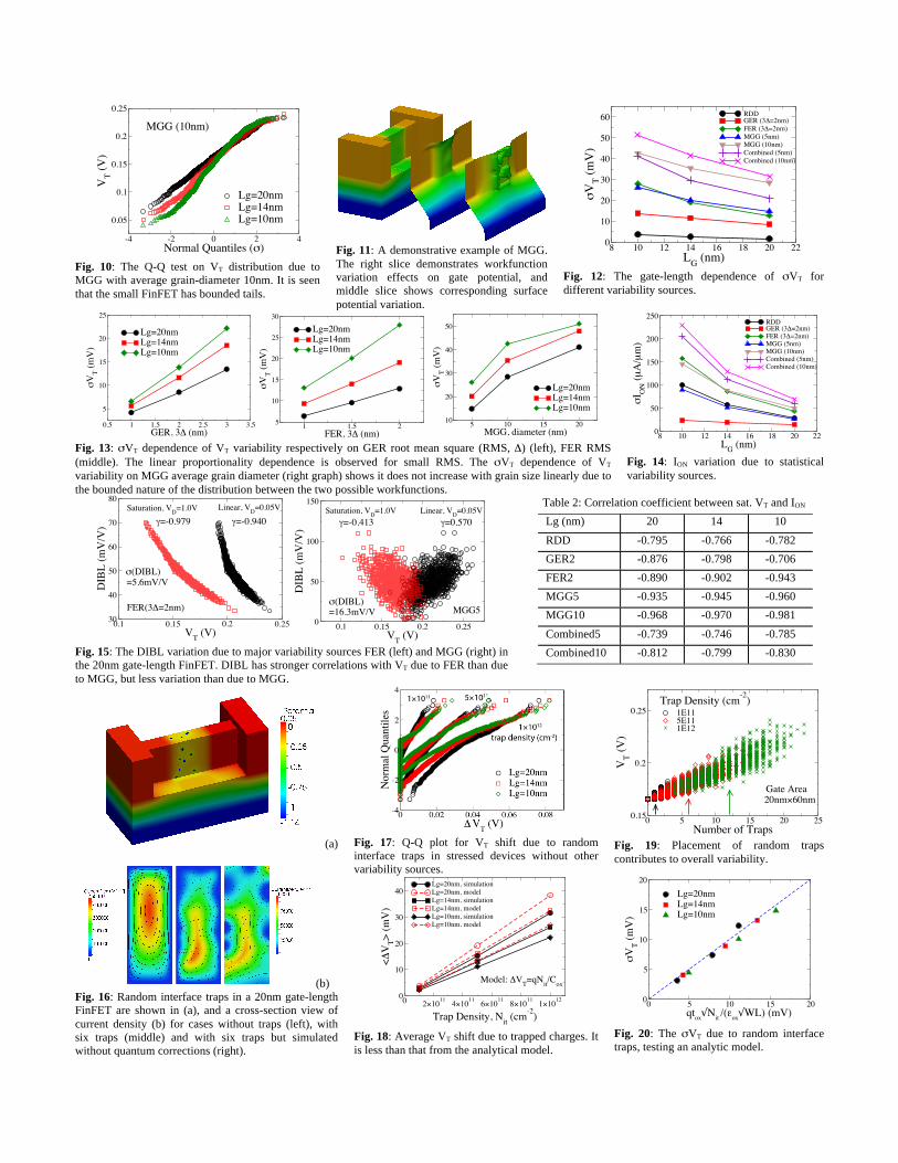
Fig. 10: The Q-Q test on VT distribution due to MGG with average grain-diameter 10nm. It is seen that the small FinFET has bounded tails.
Fig. 11: A demonstrative example of MGG. The right slice demonstrates workfunction variation effects on gate potential, and middle slice shows corresponding surface potential variation.
Fig. 12: The gate-length dependence of σVT for different variability sources.
Fig. 13: σVT dependence of VT variability respectively on GER root mean square (RMS, Δ) (left), FER RMS (middle). The linear proportionality dependence is observed for small RMS. The σVT dependence of VT variability on MGG average grain diameter (right graph) shows it does not increase with grain size linearly due to the bounded nature of the distribution between the two possible workfunctions.
Fig. 14: ION variation due to statistical variability sources.
Fig. 15: The DIBL variation due to major variability sources FER (left) and MGG (right) in the 20nm gate-length FinFET. DIBL has stronger correlations with VT due to FER than due to MGG, but less variation than due to MGG.
Table 2: Correlation coefficient between sat. VT and ION
Lg (nm) 20 14 10
RDD -0.795 -0.766 -0.782
GER2 -0.876 -0.798 -0.706
FER2 -0.890 -0.902 -0.943
MGG5 -0.935 -0.945 -0.960
MGG10 -0.968 -0.970 -0.981
Combined5 -0.739 -0.746 -0.785
Combined10 -0.812 -0.799 -0.830
(a)
(b) Fig. 16: Random interface traps in a 20nm gate-length FinFET are shown in (a), and a cross-section view of current density (b) for cases without traps (left), with six traps (middle) and with six traps but simulated without quantum corrections (right).
Fig. 17: Q-Q plot for VT shift due to random interface traps in stressed devices without other variability sources.
Fig. 19: Placement of random traps contributes to overall variability.
Fig. 18: Average VT shift due to trapped charges. It is less than that from the analytical model.
Fig. 20: The σVT due to random interface traps, testing an analytic model.
-4 -2 0 2 4Normal Quantiles ( )
0.05
0.1
0.15
0.2
0.25V
T (
V)
Lg=20nmLg=14nmLg=10nm
MGG (10nm)
8 10 12 14 16 18 20 22L
G (nm)
0
10
20
30
40
50
60
VT (
mV
)
RDDGER (3 =2nm)FER (3 =2nm)MGG (5nm)MGG (10nm)Combined (5nm)Combined (10nm)
0.5 1 1.5 2 2.5 3 3.5GER, 3 (nm)
5
10
15
20
25
VT (
mV
)
Lg=20nmLg=14nmLg=10nm
1 1.5 2FER, 3 (nm)
5
10
15
20
25
30
VT (
mV
)
Lg=20nmLg=14nmLg=10nm
5 10 15 20MGG, diameter (nm)
10
20
30
40
50
VT (
mV
)
Lg=20nmLg=14nmLg=10nm
8 10 12 14 16 18 20 22L
G (nm)
0
50
100
150
200
250
I ON
(A
/m
)
RDDGER (3 =2nm)FER (3 =2nm)MGG (5nm)MGG (10nm)Combined (5nm)Combined (10nm)
0.1 0.15 0.2 0.25V
T (V)
30
40
50
60
70
80
DIB
L (
mV
/V)
Saturation, VD
=1.0V Linear, VD
=0.05V
=-0.979 =-0.940
(DIBL)
FER(3 =2nm)
=5.6mV/V
0.1 0.15 0.2 0.25V
T (V)
0
50
100
150
DIB
L (
mV
/V)
Saturation, VD
=1.0V Linear, VD
=0.05V
=-0.413 =0.570
(DIBL)=16.3mV/V MGG5
0 5 10 15 20 25Number of Traps
0.15
0.2
0.25
VT (
V)
1E115E111E12
Trap Density (cm-2
)
20nm×60nmGate Area
0 2 1011
4 1011
6 1011
8 1011
1 1012
Trap Density, Nit (cm
-2)
0
10
20
30
40
<V
T>
(m
V)
Lg=20nm, simulationLg=20nm, modelLg=14nm, simulationLg=14nm, modelLg=10nm, simulationLg=10nm, model
Model: VT=qN
it/C
ox
0 5 10 15 20qt
ox√N
it /(ε
ox√WL) (mV)
0
5
10
15
20
σV
T (
mV
)
Lg=20nmLg=14nmLg=10nm