status of the n-xyter and cbm-xyter development line christian j. schmidt et al., gsi darmstadt...
TRANSCRIPT

Status of the
n-XYTER and CBM-XYTER
development line
Christian J. Schmidt et al.,
GSI Darmstadt
JINR, Dubna, Oct. 15th 2008

12th CBM Collaboration Meeting, Dubna, Oct. 15th 2008
n-XYTER, current workhorse chip for prototyping
workhorse readout chip for detector prototyping
architectural example front-end for DAQ development (self triggered, data driven)
sample ASIC for technological front-end electronics hybrid developments bonding technology, circuit board technology
thermal management, active cooling concepts
power management (integraly high currents, low voltage, high B-fields, high rad. environment)
very dense mechanical boundary conditions

12th CBM Collaboration Meeting, Dubna, Oct. 15th 2008
"Simple" FEB for the n-XYTER Starter Kit
A simple hybrid PCB with signal fan-in, ADC and interconnect to SysCore DAQ chain
Allow development of the DAQ chain
Allow the readout of various detector prototypes
Allow to explore the challenges of hybrid development
The September beam time has shown the whole signal chain operative!
Silicon Strip / GEM Gas Detectors --- n-XYTER --- SysCore DAQ System
12th CBM Collaboration Meeting, Dubna, Oct. 15th 2008
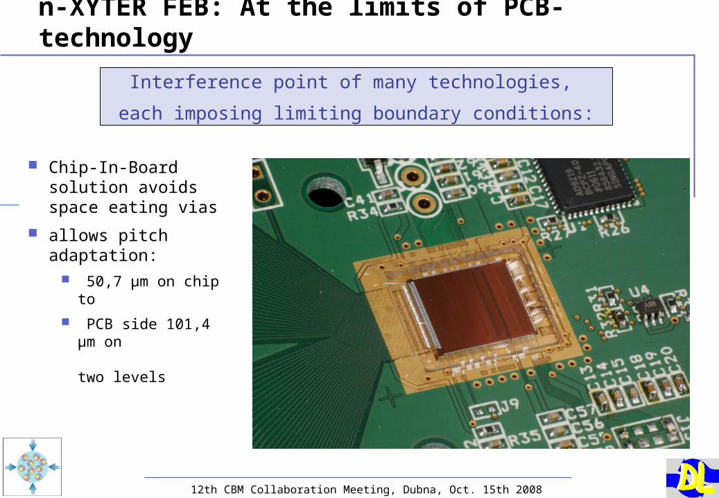
n-XYTER FEB: At the limits of PCB-technology
Chip-In-Board solution avoids space eating vias
allows pitch adaptation: 50,7 µm on chip to
PCB side 101,4 µm on two levels
Interference point of many technologies,
each imposing limiting boundary conditions:
12th CBM Collaboration Meeting, Dubna, Oct. 15th 2008
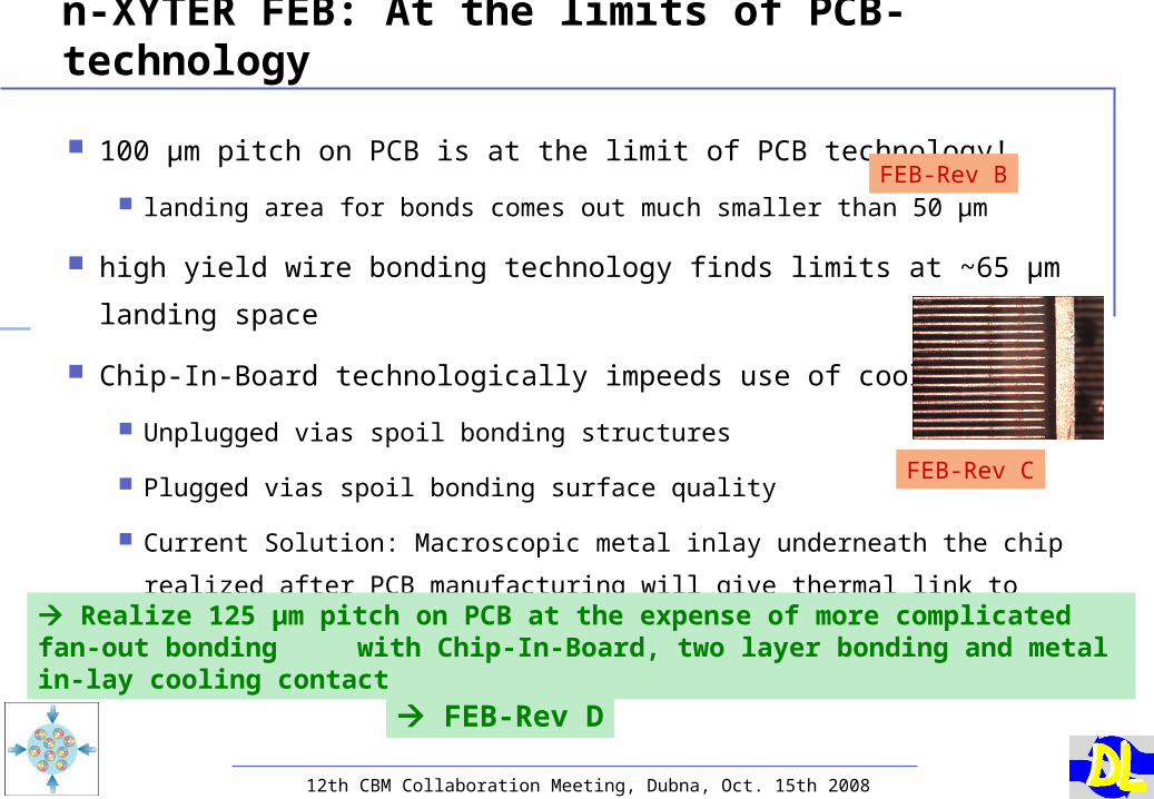
n-XYTER FEB: At the limits of PCB-technology
100 µm pitch on PCB is at the limit of PCB technology!
landing area for bonds comes out much smaller than 50 µm
high yield wire bonding technology finds limits at ~65 µm landing space
Chip-In-Board technologically impeeds use of cooling vias
Unplugged vias spoil bonding structures
Plugged vias spoil bonding surface quality
Current Solution: Macroscopic metal inlay underneath the chip realized after
PCB manufacturing will give thermal link to cooling infrastructure
FEB-Rev B
FEB-Rev C
Realize 125 µm pitch on PCB at the expense of more complicated fan-out bonding with Chip-In-Board, two layer bonding and metal in-lay cooling contact
FEB-Rev D

12th CBM Collaboration Meeting, Dubna, Oct. 15th 2008
It is all a question of yield!
PCB-Technology• 50µ / 50µ shatteres yield • close contact to manufacturer• special solutions (Chip in Board)• metal inlay solution
Wire Bonding Technology:• Maximum bond length ~ 4 mm • Staggered fan-out complicates bonding• Bonding machine determines specs on dimensions of landing space
Home made issues:-- Cooling strategy:• Wire bonds demand cooling from below • Flip-Chip bump bonds may allow cooling from either side-- Limitations on Orcad layout tool-- On Chip bond-pad layout
12th CBM Collaboration Meeting, Dubna, Oct. 15th 2008
STS specific hybrid developments Hybrid for STS Ladder Modules
Combined challenges of high density chip assembly needs
sensitive microcable detector interconnect
integrated cooling
integrated powering scheeme in high magnetic fields and rad. env.
Temptatively, a completly different technology comes into play: Silicon based circuit board
flip chip assembly of XYTERs high efficiency cooling contacts and hybrid stackability
tap bonding for micro-cables (V. Pugatch, Kiev)
separated potential domain for upper and lower side det. readout
(see STS meeting for more details)
12th CBM Collaboration Meeting, Dubna, Oct. 15th 2008
Activities in Heidelberg: Preparation of n-XYTER engineering run
n-XYTER prototype showed a large temp. coeff. due to unmatched circuitry assembled from different labs
(DETNI collaboration). The correction of it is the major modification currently realized.
A process more suited for mixed signal designs will be employed
Rearranged bond-pad lay-out will faciliate bonding
Enhanced on-chip shielding will inhibit cross-talk and inter circuit feed-back
two versions of dynamic range (120 000 e, 1000 000 e) will widen scope of applications
Hans K.Soltveit, Physik. Inst. Heidelberg
An Engineering Run of the n-XYTER will supply us with chips for detector prototyping activities!
Towards this production, some issues may be addressed.
12th CBM Collaboration Meeting, Dubna, Oct. 15th 2008
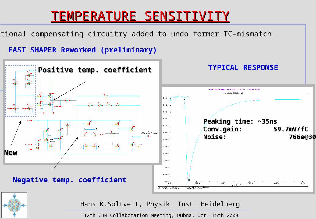
TEMPERATURE SENSITIVITYTEMPERATURE SENSITIVITY
FAST SHAPER Reworked (preliminary)
TYPICAL RESPONSE
Peaking time: ~35nsPeaking time: ~35nsConv.gain: 59.7mV/fCConv.gain: 59.7mV/fCNoise: 766e@30pFNoise: 766e@30pF
Negative temp. coefficient
Positive temp. coefficientPositive temp. coefficient
NewNew
Hans K.Soltveit, Physik. Inst. Heidelberg
Additional compensating circuitry added to undo former TC-mismatch
12th CBM Collaboration Meeting, Dubna, Oct. 15th 2008
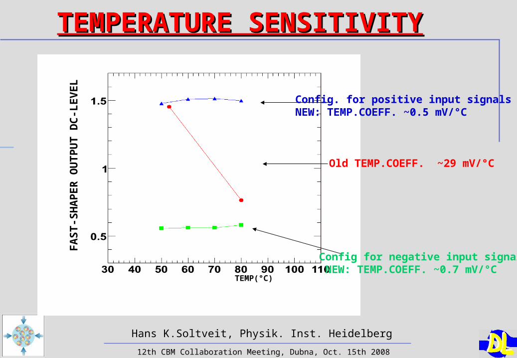
TEMPERATURE SENSITIVITYTEMPERATURE SENSITIVITY
FA
ST
-SH
AP
ER
OU
TP
UT
DC
-LE
VE
L
TEMP(°C)
Old TEMP.COEFF. ~29 mV/°C
Config for negative input signals NEW: TEMP.COEFF. ~0.7 mV/°C
Config. for positive input signals NEW: TEMP.COEFF. ~0.5 mV/°C
Hans K.Soltveit, Physik. Inst. Heidelberg
12th CBM Collaboration Meeting, Dubna, Oct. 15th 2008
Time Line towards the engineering run
Temperature compensation also realized on slow shaper
energy signal chain!
Currently: Extensive corner analysis on new schematics
Beginning of November: Review on schematical modifications
Until the end of the year: Layout modifications
Beginning of Jan.: Submission readiness review
Jan to Feb.: Submission to AMS

12th CBM Collaboration Meeting, Dubna, Oct. 15th 2008
Midterm and Beyond, the CBM XYTER
Exploit detector prototyping experiences
Self triggered architecture
Rates adapted
Radiation hard
On chip energy conversion
Efficient, low lead-count serialized data transfer
DC-coupled double sided Silicon readout
A dedicated CBM-XYTER development gets on its rails...

12th CBM Collaboration Meeting, Dubna, Oct. 15th 2008
CBM-XYTER Family Planning
CBM-STS-XYTER minimize power
realize dc-leakage compensation
compact, high channel density
MIP sensitivity in Si
dense mounting
CBM-TRD-XYTER high resolution
needs (8 to 9 bit)
lower channel density
next neighbor forced trigger logic?
ion tail cancellation facilities
baseline restauration
lower occupancy
MUCH needs are somewhere in
between.Preferably adopt
these specs within one of the two! (see
V. Niculin)
MUCH needs are somewhere in
between.Preferably adopt
these specs within one of the two! (see
V. Niculin)
Both XYTER chips will employ common rad. hard library and common design blocks for the readout FiFo and MUX (data sparcification and de-randomization), slow control interface, data transfer serializers, testability features and clocking and time stamp generation.
12th CBM Collaboration Meeting, Dubna, Oct. 15th 2008
CBM-STS-XYTER
Robert Szczygiel and Pawel Grybos (AGH Krakow) will realize the job. They share experience on the n-XYTER development within DETNI)
Pre study ongoing
MIP sensitivity with around 120 000 e dynamic range
128 channels, high density
Time over threshold (TOT) architecture extremely power saving due to less architectural overhead
low resolution needs, 4 to 5 bit
low demand on silicon real estate
Particular demands on S/N for clean discrimination
12th CBM Collaboration Meeting, Dubna, Oct. 15th 2008
CBM-TRD-XYTER
Peter Fischer et al. (ZITI Heidelberg) will realize this chip, Vasili Catanescu (NIHAM Bucharest) adds a proposal for the front-end (see
Mihai Petrovici on current test chip preparation)
The specific architectural needs for the TRD-XYTER have not entirely crystalized yet.
We intend to have a concerted workshop in Dec. 2008 with detector physicists
and electronics engineers .... to work out the TRD-XYTER spec-frame
Our discussion on this meeting should give us guidance for the preparation of this workshop.
Also, MUCH specifics should be collected to evaluate the feasibility of a combined TRD-MUCH-XYTER version.

12th CBM Collaboration Meeting, Dubna, Oct. 15th 2008