stc-10025 - swedish telecomswedishtelecom.com/wp-content/uploads/2013/03/stc-10025.pdf ·...
TRANSCRIPT

Page 1
STC-10025
1.25Gb/s 1310nm Single-mode SFP Transceiver
PRODUCT FEATURES
Up to 1.25Gb/s data links
FP laser transmitter and PIN photo-detector
Up to 10km on 9/125µm SMF
Hot-pluggable SFP footprint
Duplex LC/UPC type pluggable optical interface
Low power dissipation
Metal enclosure, for lower EMI
RoHS compliant and lead-free
Single +3.3V power supply
Support Digital Diagnostic Monitoring interface
Compliant with SFF-8472
Case operating temperature
Commercial: 0°C to +70°C
Extended: -10°C to +80°C
Industrial: -40°C to +85°C
APPLICATIONS
Switch to Switch Interface
Gigabit Ethernet
Switched Backplane Applications
Router/Server Interface
Other Optical Links
© Copyright 2013 Swedish Telecom [email protected]

Page 2
PRODUCT DESCRIPTION
STC-10025 Small Form Factor Pluggable (SFP) transceivers are compatible with the Small Form Factor
Pluggable Multi-Sourcing Agreement (MSA). The transceiver consists of five sections: the LD driver, the
limiting amplifier, the digital diagnostic monitor, the 1310nm FP laser and the PIN photo-detector .The module
data link up to 10KM in 9/125um single mode fiber.
The optical output can be disabled by a TTL logic high-level input of Tx Disable, and the system also can disable
the module via I2C. Tx Fault is provided to indicate that degradation of the laser. Loss of signal (LOS) output is
provided to indicate the loss of an input optical signal of receiver or the link status with partner. The system can
also get the LOS (or Link)/Disable/Fault information via I2C register access.
Ordering information
Product part
Number
Data
Rate
(Mbps)
Media Wavelength
(nm)
Transmission
Distance(km) Temperature Range()
STC-10025 1250 Single mode fiber 1310 10 0~70 commercial
STC-10025 1250 Single mode fiber 1310 10 -10~80 extended
STC-10025 1250 Single mode fiber 1310 10 -40~85 industrial
© Copyright 2013 Swedish Telecom [email protected]

Page 3
I. Pin Descriptions
Pin Symbol Name/Description Ref.
1 VEET Transmitter Ground (Common with Receiver Ground) 1
2 TFAULT Transmitter Fault.
3 TDIS Transmitter Disable. Laser output disabled on high or open. 2
4 MOD_DEF(2) Module Definition 2. Data line for Serial ID. 3
5 MOD_DEF(1) Module Definition 1. Clock line for Serial ID. 3
6 MOD_DEF(0) Module Definition 0. Grounded within the module. 3
7 Rate Select No connection required 4
8 LOS Loss of Signal indication. Logic 0 indicates normal operation. 5
9 VEER Receiver Ground (Common with Transmitter Ground) 1
10 VEER Receiver Ground (Common with Transmitter Ground) 1
11 VEER Receiver Ground (Common with Transmitter Ground) 1
12 RD- Receiver Inverted DATA out. AC Coupled
13 RD+ Receiver Non-inverted DATA out. AC Coupled
14 VEER Receiver Ground (Common with Transmitter Ground) 1
15 VCCR Receiver Power Supply
16 VCCT Transmitter Power Supply
17 VEET Transmitter Ground (Common with Receiver Ground) 1
18 TD+ Transmitter Non-Inverted DATA in. AC Coupled.
19 TD- Transmitter Inverted DATA in. AC Coupled.
20 VEET Transmitter Ground (Common with Receiver Ground) 1
Notes:
1. Circuit ground is internally isolated from chassis ground.
2. Laser output disabled on TDIS >2.0V or open, enabled on TDIS <0.8V.
3. Should be pulled up with 4.7k - 10kohms on host board to a voltage between 2.0V and 3.6V.MOD_DEF (0)
pulls line low to indicate module is plugged in.
4. This is an optional input used to control the receiver bandwidth for compatibility with multiple data rates (most
likely Fiber Channel 1x and 2x Rates).If implemented, the input will be internally pulled down with > 30kΩ
resistor. The input states are:
Low (0 – 0.8V): Reduced Bandwidth
(>0.8, < 2.0V): Undefined
High (2.0 – 3.465V): Full Bandwidth
Open: Reduced Bandwidth
5. LOS is open collector output should be pulled up with 4.7k - 10kohms on host board to a voltage between 2.0V
and 3.6V. Logic 0 indicates normal operation; logic 1 indicates loss of signal.
© Copyright 2013 Swedish Telecom [email protected]

Page 4
Figure2. Pin out of Connector Block on Host Board
II. Absolute Maximum Ratings
III. Recommended Operating Conditions
Parameter Symbol Min. Typ. Max. Unit Note
Storage Temperature Ts -40 85 ºC
Storage Ambient Humidity HA 5 95 %
Power Supply Voltage VCC -0.5 4 V
Signal Input Voltage -0.3 Vcc+0.3 V
Receiver Damage Threshold +5 dBm
Parameter Symbol Min. Typ. Max. Unit Note
Case Operating Temperature Tcase
0 70
ºC
STC-10025
-10 80 STC-10025
-40 85 STC-10025
Ambient Humidity HA 5 70 % Non-condensing
Power Supply Voltage VCC 3.13 3.3 3.47 V
Power Supply Current ICC 280 mA
Power Supply Noise Rejection 100 mVp-p 100Hz to 1MHz
Data Rate 1250/1250 Mbps TX Rate/RX Rate
Transmission Distance 10 KM
Coupled Fiber Single mode fiber 9/125um SMF
© Copyright 2013 Swedish Telecom [email protected]

Page 5
IV. Specification of Transmitter
Note (1): Measure at 2^7-1 NRZ PRBS pattern.
Note (2): Transmitter eye mask definition
V. Specification of Receiver
Note (1): Measured with Light source 1310nm, ER=9dB; BER =<10^-12 @PRBS=2^7-1 NRZ.
Note (2): When SD De-Assert, the RX-LOS output is signal output.
Parameter Symbol Min. Typ. Max. Unit Note
Average Output Power POUT -9 -3 dBm
Extinction Ratio ER 9 dB
Center Wavelength λC 1270 1310 1360 nm FP Laser Spectrum Bandwidth(RMS) σ 3.5 nm
Transmitter OFF Output Power POff -45 dBm
Differential Line Input Impedance RIN 90 100 110 Ohm
Jitter P-P tJ 0.1 UI Note (1) Output Eye Mask Compliant with IEEE802.3 z (class 1
laser safety) Note (2)
Parameter Symbol Min. Typ. Max. Unit Note
Input Optical Wavelength λIN 1270 1610 nm PIN-TIA
Receiver Sensitivity PIN -19 dBm Note (1)
Input Saturation Power (Overload) PSAT -3 dBm
Los Of Signal Assert PA 38 dBm
Los Of Signal De-assert PD - -20 dBm Note (2)
LOS Hysteresis PA-PD 0.5 2 6 dB
© Copyright 2013 Swedish Telecom [email protected]

Page 6
VI. Electrical Interface Characteristics
Note (1): A (TX) + B (RX) = 280mA (Not include termination circuit)
VII. Digital Diagnostic Functions
Swedish Telecom STC-10025 transceivers support the 2-wire serial communication protocol as defined in the SFP MSA. It is very closely related to the E2PROM defined in the GBIC standard, with the same electrical specifications. The standard SFP serial ID provides access to identification information that describes the transceiver’s capabilities, standard interfaces, manufacturer, and other information.
Additionally, Swedish Telecom SFP transceivers provide a unique enhanced digital diagnostic monitoring interface, which allows real-time access to device operating parameters such as transceiver temperature, laser bias current, transmitted optical power, received optical power and transceiver supply voltage .It also defines a sophisticated system of alarm and warning flags, which alerts end-users when particular operating parameters are outside of a factory set normal range.
The SFP MSA defines a 256-byte memory map in E2PROM that is accessible over a 2-wire serial interface at the 8 bit address 1010000X (A0h). The digital diagnostic monitoring interface makes use of the 8 bit address 1010001X (A2h), so the originally defined serial ID memory map remains unchanged. The interface is identical to, and is thus fully backward compatible with both the GBIC Specification and the SFP Multi Source Agreement.
The operating and diagnostics information is monitored and reported by a Digital Diagnostics Transceiver Controller (DDTC) inside the transceiver, which is accessed through a 2-wire serial interface. When the serial protocol is activated, the serial clock signal (SCL, Mod Def 1) is generated by the host. The positive edge clocks data into the SFP transceiver into those segments of the E2PROM that are not write-protected. The negative edge clocks data from the SFP transceiver. The serial data signal (SDA, Mod Def 2) is bi-directional for serial data transfer. The host uses SDA in conjunction with SCL to mark the start and end of serial protocol activation. The memories are organized as a series of 8-bit data words that can be addressed individually or sequentially.
Digital diagnostics for the STC-10025 are internally calibrated by default.
Parameter Symbol Min. Typ. Max. Unit Note Transmitter
Total Supply Current ICC A mA Note (1)
Transmitter Disable Input-High VDISH 2 Vcc+0.3 V
Transmitter Disable Input-Low VDISL 0 0.8 V
Transmitter Fault Input-High VDISL 2 Vcc+0.3 V
Transmitter Fault Input-Low VTxFH 0 0.8 V
Receiver
Total Supply Current ICC B mA Note (1)
LOSS Output Voltage-High VLOSH 2 Vcc+0.3 V LVTTL
LOSS Output Voltage-Low VLOSL 0 0.8 V
© Copyright 2013 Swedish Telecom [email protected]

Page 7
VIII. Recommend Circuit Schematic
VccR
3.3V
VeeT
Amplifier
EEPROM
0.1uF
VeeR
0.1uF
Rx_LOS
1uH
SerDes IC
1uH
100 Ohm
RES1
VCC
TD+
TD-
RES1
Protocol Vcc
Rx_LOS
0.1uF
0.1uF
Tx_Disable
Tx_Fault
0.1uF
10uF
10uF
* Depands onSerDes IC used
RES1=4.7K to10K Ohms
100 Ohm
RD+
RD-
Tx_Fault
Mod_def 2
PLD/PAL
Photo Diode
Laser Diode
Tx_Disable
Mod_def 0
3.3V
10K
RES1 RES1
VccT
RES1
0.1uF
Mod_def 1
10uF
Swedish Telecom SFP Module
Protocol IC
0.1uF
Laser Driver
© Copyright 2013 Swedish Telecom [email protected]
Page 8
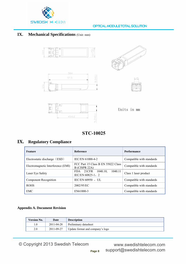
IX. Mechanical Specifications (Unit: mm)
STC-10025
IX. Regulatory Compliance
Feature Reference Performance
Electrostatic discharge(ESD) IEC/EN 61000-4-2 Compatible with standards
Electromagnetic Interference (EMI) FCC Part 15 Class B EN 55022 Class B (CISPR 22A)
Compatible with standards
Laser Eye Safety FDA 21CFR 1040.10, 1040.11 IEC/EN 60825-1,2
Class 1 laser product
Component Recognition IEC/EN 60950 ,UL Compatible with standards
ROHS 2002/95/EC Compatible with standards
EMC EN61000-3 Compatible with standards
Appendix A. Document Revision
Version No. Date Description
1.0 2011-04-28 Preliminary datasheet
2.0 2011-09-27 Update format and company’s logo
© Copyright 2013 Swedish Telecom [email protected]