stm manipulation
TRANSCRIPT

7/27/2019 stm manipulation
http://slidepdf.com/reader/full/stm-manipulation 1/19
IOP PUBLISHING JOURNAL OF PHYSICS: CONDENSED MATTER
J. Phys.: Condens. Matter 20 (2008) 053001 (19pp) doi:10.1088/0953-8984/20/05/053001
TOPICAL REVIEW
Functionalized molecules studied by STM:motion, switching and reactivity
Leonhard Grill
Institut fur Experimentalphysik, Freie Universitat Berlin, Arnimallee 14, 14195 Berlin,
Germany
E-mail: [email protected]
Received 2 November 2007, in final form 5 December 2007
Published 8 January 2008Online at stacks.iop.org/JPhysCM/20/053001
Abstract
Functionalized molecules represent the central issue of molecular nanotechnology. Scanning
tunnelling microscopy (STM) is a powerful method to investigate such molecules, because it
allows us to image them with sub-molecular resolution when adsorbed on a surface and can be
used at the same time as a tool to manipulate single molecules in a controlled way. Such studies
permit deep insight into the conformational, mechanical and electronic structure and thus
functionalities of the molecules. In this review, recent experiments on specially designed
molecules, acting as model systems for molecular nanotechnology, are reviewed. The presented
studies focus on key functionalities: lateral rolling and hopping motion on a supporting surface,
the switching behaviour of azobenzene derivatives by using the STM tip and the controlled
reactivity of molecular side groups, which enable the formation of covalently bound molecularnanoarchitectures.
(Some figures in this article are in colour only in the electronic version)
Contents
1. Introduction 1
2. Motion 4
2.1. Lateral manipulation of molecules 4
2.2. Rolling a molecular wheel 5
3. Molecular switches 73.1. Growth of azobenzene derivatives on Au(111) 8
3.2. Isomerization 8
4. Covalent intermolecular connections 11
4.1. Bond formation by activation of molecular side
groups 12
4.2. Nanoarchitecture 13
5. Outlook 16
Acknowledgments 17
References 18
1. Introduction
The fascinating vision of molecular nanotechnology lies inthe use of single molecules as machines or devices and the
controlled assembly of molecular matter at the nanometre
scale (nanomanufacturing). The possibility to manipulate and
control things on a small scale was first introduced by Richard
Feynman in his famous 1959 speech ‘There’s plenty of room
at the bottom’ [1]. Resulting applications, like electronic
circuits, sensors or nanomachines, would, due to their small
dimensions, open the door to completely new technologies,with advantages in cost, operation speed (efficiency) and power
dissipation. In contrast to top-down approaches (e.g. by
improving lithographic techniques), the use of molecules
reveals several important advantages:
(1) Molecules have nanoscale dimensions by nature: thus,
the use of single molecules automatically leads to
structural dimensions at the atomic scale. The top-
down miniaturization of existing applications and devices
requires fundamental improvements of conventional
fabrication techniques, which are limited.
(2) Molecular recognition: intermolecular interactions can
be used to grow molecular nanostructures. Moleculesare known to self-organize according to their chemical
0953-8984/08/053001+19$30.00 © 2008 IOP Publishing Ltd Printed in the UK1

7/27/2019 stm manipulation
http://slidepdf.com/reader/full/stm-manipulation 2/19
J. Phys.: Condens. Matter 20 (2008) 053001 Topical Review
Figure 1.1. Principle of biosensors. Two nanowire devices (1 and 2) are modified with different (1, green; 2, red) antibody receptors.
A cancer marker protein that binds specifically to its receptor (on nanowire 1) will produce a conductance change characteristic of the surfacecharge of the protein only on nanowire 1. From Lieber and co-workers. Reproduced with permission from [5]. Copyright (2005) NaturePublishing Group.
properties and to self-assemble in topologies that reflect
the interactions between them. By controlling the
chemistry of the involved molecules, various structures of
different size and shapes can be produced.
(3) Capabilities of organic chemistry: by choosing the
structure and composition of a molecule, chemical
synthesis can be used to produce molecules of precisely
defined properties.
(4) Functions: molecules can have specific functions,for instance switching between different states (of
characteristic optical, magnetic and electronic properties).
In fact, this is a fundamental concept in nature, where
many molecules have multiple stable isomers.
These characteristics make molecules very suitable for
applications in the field of molecular nanotechnology, which
divides into several sub-topics. Some main issues are discussed
in the following.
The high selectivity caused by molecular recognition is
of great interest for the development of so-called intelligent
materials, where molecules act as highly sensitive detectors
for another specific type of molecule or nanoparticle. Afamous example in this context is the so-called artificial nose,
where differently coated cantilevers are used to characterize
vapours [2]. Intense research activities in this field are focusing
on biosensors [3, 4], which contain biological components like
proteins, enzymes or antibodies that bind (or do not bind)
selectively to a substance of interest. This concept is illustrated
in figure 1.1, where two nanowires are equipped with different
receptors [5]. After exposing the device to specific cancer
marker proteins, only one nanowire is modified while the other
one remains intact. Additional to the biologically sensitive
part, such sensors require the detection of a signal related to the
chemical processes. In figure 1.1, this is achieved by a changein the conductance properties of nanowire 1, while nanowire
2 remains unchanged. Thus, proteins are detected electrically
with extremely high sensitivity, as only very small quantities of
the detected substance are required. Furthermore, the process
is highly selective, because the receptors exclusively bind to
the proteins in question. Additionally to the electric detection,
an important class of biosensors is based on the change of
optical properties like absorbance, fluorescence or refractive
index [6].
Another key topic of molecular nanotechnology is
nanomachines, which control motion at the atomic scale [7, 8].
A nanomachine must, like any macroscopic machine, perform
useful functions. It should contain a motor, where the energysupply (e.g. light, electric field, chemical environment, electric
current) plays an important role. Such molecules can be
synthesized completely, even though this is a difficult task
for organic chemistry if the functionality and complexity
is increasing, or assembled from various building blocks
to supramolecular systems [9]. The major challenge in
operating nanomachines is not only to achieve molecular
motion, but also to control and read out the operation. An
important issue in this regard is the information exchange
with the macroscopic world, i.e. to control and prove thefunctionality of the nanomachines experimentally. It is not
sufficient to detect that motion occurs, because for optimizing
a nanomachine’s operation a detailed understanding of the
intramolecular processes is necessary. Finally, in order to
approach useful nanomachines, the timescale of the operation
and the possibility to repeat the operation in cycles are
important properties.
Although the concepts of molecular machines are often
similar to macroscopic machines, they cannot simply be
considered as miniaturized versions, because matter behaves
differently at the nanoscale. Gravitational forces and inertia
can be neglected, due to small mass, and motion is dominatedby physical/chemical interactions with molecules of the
environment, for instance solution, or a supporting surface. On
the other hand, thermal fluctuations (Brownian motion) are not
important for macroscopic objects, but strongly prevail at the
nanoscale [10].
Many approaches towards molecular nanomachines take
advantage of concepts and processes that are known from
nature. One example is DNA-based nanomachines, which
are very suitable for the construction of three-dimensional
objects by self-assembly, controlling their interaction through
base sequences [11, 12]. By means of molecular motion, the
protein family of myosins are very interesting, because theirtranslational motion is similar to a ‘walking’ mechanism [13].
Much smaller molecules, based on an anthracene board,
with in fact atomic scale dimensions, have been reported
recently to move in a ‘walking’ mode, even ‘carrying’ CO2
molecules [14, 15]. The rolling motion of carbon nanotubes
on a graphite surface has been reported by directly imaging the
different stages with an atomic force microscope (AFM) [16].
Furthermore, several molecular rotors [17] and surface-rolling
molecules [18] have been proposed.
Figure 1.2 shows one of the most famous examples of
a nanomachine, the rotaxane [9, 19, 20]. This molecule is
considered as a molecular elevator, because the macrocyclic
ring in its centre is mobile along the central molecular axis.Bulky groups that avoid disassembly of the supramolecular
2

7/27/2019 stm manipulation
http://slidepdf.com/reader/full/stm-manipulation 3/19
J. Phys.: Condens. Matter 20 (2008) 053001 Topical Review
a
b
Figure 1.2. Principle of a ‘molecular elevator’. (a) Schematic representation and (b) chemical structure of a bistable [2] rotaxane, containingtwo different recognition sites, to one of which the ring component is attracted much more than the other. The two different states of themolecule can be switched by an external stimulus, such as a change in pH. From [19]. Reprinted with permission from AAAS.
system terminate the axis. An important property of this
molecular machine are the non-covalent interactions between
the ring and the central board, allowing the motion of themacrocycle between different stable sites, where it is stabilized
by hydrogen bonds orπ–π stacking. By changing the chemical
environment of the rotaxane between acid and base, the
preferred position of the ring changes accordingly and it moves
up and down, as shown in figure 1.2(b). It has been shown
that this motion can also be induced by visible light [21], thus
enabling different energy supplies of this ‘motor’.
An important section of molecular nanotechnology is
molecular electronics, the miniaturization of electronic devices
to the atomic scale. As the top-down approach of the
semiconductor industry, following Moore’s law that transistor
density doubles every three years [22], will reach its physical
limits in the foreseeable future, devices of the size of singleatoms or molecules will be required [23]. Hence, completely
new strategies for the fabrication of nanocircuits at the
molecular scale are necessary [24–28]. The ultimate goal
is that single functionalized molecules are used as electronic
devices connected by nanoscale wires.
Aviram and Ratner proposed as early as 1974 that a single
molecule can act as a rectifier [29]. This concept, presented in
figure 1.3, is based on the asymmetric conductance behaviour
due to the donor–spacer–acceptor structure of the molecule.
Similarly, the chemical structure of more complex molecules
can be modified in order to design for example molecular
wires or switches [24]. However, the first experimentalstudies of molecular devices were done more than 20 years
later, when the conductivity through single molecules was
investigated [30]. Molecular rectifiers, as proposed by Aviram
and Ratner, were realized in a multilayer [31] or using
single fullerene molecules [32] and the conductance was
switched through conformational changes of the molecule [33].
An important class of molecules in this regard are carbon
nanotubes with their characteristic physical properties [34].
Experiments have studied their conductivity [35], even over
large distances of 1 μm [36], and their ability to be used
in a transistor, by switching them from a conducting to an
insulating state [37].
Additional to functionalized molecular devices, the wiresand contacts represent the backbone of such a nanocircuit, as
Figure 1.3. Energy versus distance of a single molecule rectifierdevice (schematic). B and D are the affinity levels and A and C thehighest occupied levels, of acceptor and donor, respectively. Byapplying a bias voltage between the two metal electrodes, themolecular orbital levels shift with respect to the metal Fermi levelsand to each other. Accordingly, the molecule exhibits different
conductivities for the two bias polarities. Reprinted with permissionfrom [29]. Copyright (1974) Elsevier.
they must enable efficient charge transport between the devices
and electrodes. It is clear that the conductivity of molecular
wires depends strongly on their chemical structure, as shown
for a variety of possible molecular wires [38, 39]. On the
other hand, the charge transport through contacts to other
molecular devices or electrodes plays a fundamental role in the
quality of a molecular device or any nanocircuit [40, 41]. It
turned out that it is at least as important for the conductivity
characteristics of a metal–molecule–metal system as themolecular core [42].
The preparation of nanocircuits from wires and functional
building blocks is an important challenge, because molecules
must be assembled efficiently in complex structures in an
autonomous way [43]. While the ability of nanostructuring
the supporting surfaces is important on the one hand [44],
molecular recognition is a suitable tool to engineer the
molecular structures [45, 46]. It has been shown that molecules
are self-organizing through their interaction in various pre-
defined topologies, even though mainly weak intermolecular
bonds, with poor thermal stability, are explored [47, 48].
An important approach to determine the conductivity of
a molecule between two electrodes is the so-called break junction, where a microfabricated electrode is broken at
3
7/27/2019 stm manipulation
http://slidepdf.com/reader/full/stm-manipulation 4/19
J. Phys.: Condens. Matter 20 (2008) 053001 Topical Review
its centre by mechanical deformation and the resistance
of the metallic wire junction is measured [49]. In
this way, the conductivity of very few molecules, which
remain in the junction, can be determined directly, having
the molecules strongly coupled by thiol groups to gold
electrodes [50]. However, its application to single molecules
is not straightforward because the conformation, environmentand exact number of interconnected molecules remain difficult
to determine [51].
The scanning tunnelling microscope (STM) is a powerful
technique as it allows us to characterize and image precisely
a single molecule (and its surrounding area) with sub-
molecular resolution and to obtain information about its
electronic and vibrational structure. Moreover, it can act
as a tool to manipulate single molecules (and atoms) and
thus to precisely probe their functions. Manipulation of
molecules intends a controlled change in their position or
conformation, a modification of their chemical or electronic
structure or inducing chemical reactions. In order to
suppress thermal motion of atoms and molecules and by
means of experimental stability, the operation of the STM at
low temperatures is advantageous. Experiments show that
molecular displacement or conformational changes within a
molecule can be mechanically induced by the STM tip [52–54].
Moreover, the tunnelling electrons can be used to induce
several processes, for instance molecular rotation [55, 56]
and vibration [57], by electronically/vibrationally exciting
molecules [58]. Diffusion [59] or desorption [60] of molecules
adsorbed on surfaces can be induced by the intense electric
field present between the STM tip and the sample surface.
Hence, the STM offers the possibility of creating a desired
geometry by means of lateral displacement on a surface. Itshould be mentioned that manipulationof single atoms can also
be done by atomic force microscopy (AFM) [61], which is of
interest for non-conducting substrates.
This work presents experiments on functionalized
molecules obtained with a (homebuilt [62]) low temperature
STM (LT-STM) working at cryogenic temperatures around 5 K
(the experimental set-up is described elsewhere [52]). The
results focus on functionalized molecules, which represent
model systems for several components in future applications
of molecular nanotechnology and molecular electronics,
adsorbed on metal surfaces. The substrate is acting on the one
hand simply as a supporting surface and on the other hand as an
electrode (while the other electrode is given by the STM tip).
2. Motion
The controlled manipulation of single molecules on surfaces
with the tip of a scanning tunnelling microscope is of
great interest for a detailed understanding of the molecular
functions. Intramolecular conformations or molecular
adsorption positions/geometries can be achieved on a surface
which often would not be present after sample preparation,
because they are energetically not favoured. At cryogenic
temperatures (where molecular manipulation is usually done),
instead, molecular configurations are ‘frozen’ due to thesmall thermal energy available. Furthermore, manipulation
experiments not only give detailed insight into the molecular
configurations and motions on a surface, but also represent
a very interesting set-up for the study of interatomic forces
(between STM tip and molecule) at atomic scale distances [63].
The various forces, active in such a junction, can in a first
approximation be described by the Lennard-Jones potential (as
a function of the interatomic distance between two noble gasatoms), consisting of attractive and repulsive interactions. The
repulsive forces can, in contrast to the attractive ones, become
very large at small interatomic separations. In the case of
STM manipulation, chemical interactions and the role of the
tunnelling current and the applied electric field must be taken
into account. These forces can be studied during manipulation
with high spatial precision if the relevant parameters (lateral
and vertical tip position, applied bias voltage, tunnelling
current) are systematically modified.
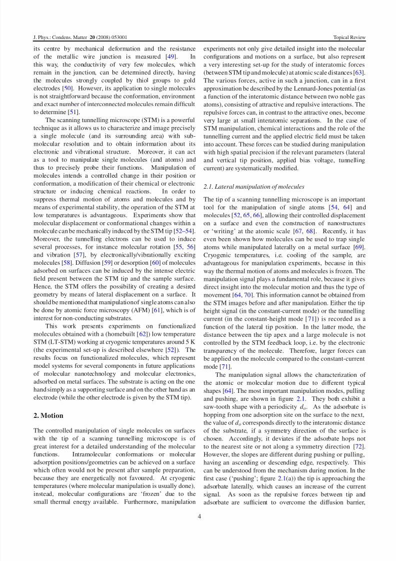
2.1. Lateral manipulation of molecules
The tip of a scanning tunnelling microscope is an important
tool for the manipulation of single atoms [54, 64] and
molecules [52, 65, 66], allowing their controlled displacement
on a surface and even the construction of nanostructures
or ‘writing’ at the atomic scale [67, 68]. Recently, it has
even been shown how molecules can be used to trap single
atoms while manipulated laterally on a metal surface [69].
Cryogenic temperatures, i.e. cooling of the sample, are
advantageous for manipulation experiments, because in this
way the thermal motion of atoms and molecules is frozen. The
manipulation signal plays a fundamental role, because it gives
direct insight into the molecular motion and thus the type of
movement [64, 70]. This information cannot be obtained fromthe STM images before and after manipulation. Either the tip
height signal (in the constant-current mode) or the tunnelling
current (in the constant-height mode [71]) is recorded as a
function of the lateral tip position. In the latter mode, the
distance between the tip apex and a large molecule is not
controlled by the STM feedback loop, i.e. by the electronic
transparency of the molecule. Therefore, larger forces can
be applied on the molecule compared to the constant-current
mode [71].
The manipulation signal allows the characterization of
the atomic or molecular motion due to different typical
shapes [64]. The most important manipulation modes, pullingand pushing, are shown in figure 2.1. They both exhibit a
saw-tooth shape with a periodicity d o. As the adsorbate is
hopping from one adsorption site on the surface to the next,
the value of d o corresponds directly to the interatomic distance
of the substrate, if a symmetry direction of the surface is
chosen. Accordingly, it deviates if the adsorbate hops not
to the nearest site or not along a symmetry direction [72].
However, the slopes are different during pushing or pulling,
having an ascending or descending edge, respectively. This
can be understood from the mechanism during motion. In the
first case (‘pushing’; figure 2.1(a)) the tip is approaching the
adsorbate laterally, which causes an increase of the current
signal. As soon as the repulsive forces between tip and
adsorbate are sufficient to overcome the diffusion barrier,
4

7/27/2019 stm manipulation
http://slidepdf.com/reader/full/stm-manipulation 5/19
J. Phys.: Condens. Matter 20 (2008) 053001 Topical Review
Figure 2.1. Principle of the lateral manipulation of an adsorbate on asurface by using the STM tip [64]. Either repulsive or attractive
forces are driving the process, leading to a ‘pushing’ (a) or ‘pulling’mode (b), respectively. The tip is moving in the schematics (left)according to the arrow. The manipulation signal (current curve atconstant tip height), plotted to the right, reveals characteristic shapesand the periodicity d o of the substrate.
the adsorbate hops to the next site. At the same time, the
current signal drops abruptly and, subsequently, the next cycle
starts with an ascending edge. The process is similar, but
inverted, in the case of a pulling mode. Note that in any
case the manipulation signal allows us to follow the atomic
or molecular motion in real time. In addition to experiments,
theory helps in the interpretation of the signals by simulatingSTM manipulation curves and can thus give precise details of
the atomic or molecular motion [73–75].
The controlled manipulation of molecules on a surface is
on the one hand of interest for the creation of nanostructures
by the bottom-up assembly of matter at the atomic scale. On
the other hand, it is the only way to bring single molecules into
particular adsorption configurations which do not correspond
to the energy minimum and are therefore not observed after
deposition, and to obtain a detailed understanding of molecular
‘nanomechanics’ during such a motion. These capabilities are
important for the development of molecular nanomachines [8].
2.2. Rolling a molecular wheel
Molecular machines, i.e. single molecules consisting of
functional components, are a fascinating challenge in
molecular nanotechnology [17]. The design of such a machine
requires a detailed understanding of its mechanical motion [8].
Several studies in the last years have shown how molecules
can be laterally displaced on a surface with high precision (see
section 2.1). However, mainly hopping motions of molecules
have been observed so far [52, 68, 76].
The best candidates for rolling motions are at first
glance fullerenes, because they exhibit a spherical shape.
Accordingly, the only clear example of a rolling molecule sofar is a carbon nanotube, which is rolled on a graphite surface
a b
Figure 2.2. (a) Chemical structure of the wheel-dimer molecule(C44H24). (b) Scheme of a manipulation with the STM tip to induce arolling motion (arrows indicate the tip movement and the rotation of the wheels, respectively). Reproduced with permission from [78].Copyright (2007) Nature Publishing Group.
using an AFM tip [16]. However, the dimensions of this
molecule exceed the atomic scale, having a tube circumference
of 83 nm. On the other hand, the STM manipulation signal of a
single C60
molecule on Si(100) was reported and presents a fine
structure superimposed on the periodic manipulation ‘hopping’
signal, which was interpreted as a rotation of the fullerene
during its hopping from one adsorption site to the next [77].
However, wheels are of greater interest by means of molecular
machines, because their rolling motion should be directional.
But so far, no rolling of a wheel has been demonstrated so at
the nanoscale, even though this is a very useful motion at the
macroscopic scale.
The rotation of single wheel molecules on metal surfaces
has been induced thermally [79] or by STM manipulation [80],
but in all cases the wheel was adsorbed flat on the surface,
i.e. having its rotational axis perpendicular to the surface,
and therefore unsuitable for the displacement of a molecularmachine. A nanocar was synthesized by mounting four C60
molecules as wheels on a non-rigid molecular board [18], but
no manipulation signal was reported to assess the possible
rotation of these C60 wheels [81]. Wheel-shaped triptycene
groups were mounted on a wheelbarrow molecule [82], but
it was not possible to displace this molecule on the surface
without modifying it.
Figure 2.2(a) presents the wheel-dimer molecule (C44H24),
where two triptycene wheels are connected via a C≡C–C≡C
axle. When adsorbed on a metal surface, this molecule exhibits
two intramolecular degrees of freedom: the independent
rotation of each wheel around the central axle. In orderto induce a rolling motion by lateral STM manipulation (as
schematically presented in figure 2.2(b)), a Cu(110) surface
was chosen, which exhibits an anisotropic corrugation due to
its close-packed rows of copper atoms in the [110] direction.
After deposition at room temperature, the molecules first
saturate the step edges and then adsorb as isolated molecules
on the Cu(110) terraces.
For a rolling motion, the orientation of the molecules
with respect to the surface directions is of great importance.
The wheel-dimer molecules adsorb in various orientations,
in particular both with the molecular axle parallel and
perpendicular to the copper rows. The STM image of a wheel-
dimer is symmetric in these cases, with apparent wheel heightsof 3.0 ± 0.2 A. The most interesting configuration is the one
5

7/27/2019 stm manipulation
http://slidepdf.com/reader/full/stm-manipulation 6/19
J. Phys.: Condens. Matter 20 (2008) 053001 Topical Review
Figure 2.3. (a) STM image (3 × 3 nm2) of a wheel-dimer molecule,oriented along the close-packed copper rows, before themanipulation and (b) the corresponding scheme (the arrows mark thepathway). Reproduced with permission from [78]. Copyright (2007)Nature Publishing Group.
Figure 2.4. Tunnelling current signals during lateral manipulation:hopping (a) and rolling motion (b). While the periodicity of thesignals in (a) corresponds to the atomic distances of the substrate, therolling motion (b) exhibits a completely new, hat-shaped signal.Reproduced with permission from [78]. Copyright (2007) NaturePublishing Group.
having the molecular axle parallel to the copper rows of the
substrate (figure 2.3), because the corrugation of the substrate
becomes most efficient for a manipulation perpendicular to
them. Calculations of the molecular conformation in this
orientation show that the central molecular axle is located
above a close-packed copper row and the lower benzene ringsof the wheels are distorted as a result of their chemisorption
on the Cu(110) surface [78]. The calculated STM image is in
very good accordance with the experimental ones, consisting
of two lobes at a distance of 8.7± 0.3 A, which corresponds to
the intramolecular distance between the two wheels of a single
molecule.
Lateral motion of the molecules across the molecular
axle (as indicated in figure 2.3) leads to typical periodic
manipulation signals as presented in figure 2.4(a). These
saw-tooth-shaped signals can be assigned to a pushing
(ascending edge) and a pulling (descending edge) mode of
manipulation [64]. The 3.6 A periodicity of these signals
corresponds to the distance between two atomic rows onthe Cu(110) surface. Hence, the molecule is hopping from
Figure 2.5. Scheme of the rolling mechanism: step (1) is the tipapproach towards the molecule, the second step (2) is a 120◦ rotationof a wheel around its molecular axle and in the last step (3) the tipreaches the other side of the molecule. It shows that in principle onlyone rotation of a wheel can be induced (the direction of movement ismarked by arrows). Reproduced with permission from [78].Copyright (2007) Nature Publishing Group.
one adsorption site (i.e. copper row) to the next during the
manipulation.
However, these are not the only observed signals. Also
a completely different manipulation signal (figure 2.4(b)) hasbeen recorded that is assigned to the rolling of a wheel within
the molecule. Several arguments confirm this interpretation:
first, the periodicity of the recorded signal is about 7 A and
therefore corresponds to a lateral motion of a wheel after a
120◦ rotation around the molecular axle (see figure 2.2(b)).
Second, a standard hopping motion over two adsorption sites
can be excluded because the signal does not show any pulling
or pushing signature, which should be the case even during
hopping over larger distances [72]. Instead, this hat-shaped
signal exhibits one intense peak at the centre and smaller
maxima on both sides. Even though the intensity distribution
slightly changes from one case to another, the overall shape
remains the same and has been recorded many times. Animportant difference between the two types of motions is that
a rolling manipulation is always obtained at larger tip heights
(vertical feed z 4 A; the initial tip height is about 7 A)
as compared to a hopping signal where the tip apex must be
approached further down towards the surface ( z 4 A).
Hence, it is possible to choose in the experiment in a controlled
way which kind of motion should be induced.
From the experimental results, the following mechanism
is proposed in figure 2.5: the tip, at sufficiently large tip
heights, induces a rolling motion of the molecular wheel,
which undergoes a rotation of 120◦. Notice that the hat-
shaped signal is mirror symmetric, in contrast to the saw-tooth-shaped signal of a hopping mode. This observation
is in accordance with the schematic model of the rolling
mechanism [83], because the first and third steps are similar
and therefore give rise to a comparable tunnelling current.
The central step (2) reveals a more intense signal, due to the
particular configuration of the molecule in this case, probably
being oriented upright as proposed in figure 2.5.
The role of the surface corrugation becomes clear if
manipulation experiments in various surface directions are
compared. If the same lateral manipulation is performed on
a molecule oriented perpendicular to the copper rows, the
manipulation signal shows a clear pushing signature with a
2.5 A periodicity, reflecting the close-packed structure alongthe rows. However, no rolling signal has ever been recorded for
6

7/27/2019 stm manipulation
http://slidepdf.com/reader/full/stm-manipulation 7/19
J. Phys.: Condens. Matter 20 (2008) 053001 Topical Review
Figure 2.6. STM images (9 × 9 nm2) before (a) and after (b) arolling manipulation. The arrow marks the pathway of the tip apexduring the manipulation and dashed lines indicate the initial positionof the wheel-dimer molecule. Tunnelling current signals during arolling manipulation are plotted in (c) and (d), revealing differentnumbers of hat-shaped signals. Reproduced with permissionfrom [78]. Copyright (2007) Nature Publishing Group.
this set-up, because the anisotropic Cu(110) surface exhibits a
much smaller corrugation in this direction [78]. A comparison
with another surface orientation of the substrate, Cu(100),
confirms this interpretation, as there very regular characteristic
pulling and pushing signals were also recorded, but no
evidence of a rolling signal has been found [78]. This is in
agreement with the rather small corrugation of the Cu(100)
surface, compared to Cu(110). Thus, due to the chemical
structure of the wheel, a rolling motion occurs only if the
molecule is manipulated perpendicular to its axle and along
a surface direction of sufficient corrugation.
An important characteristic of the two kinds of motions
arises from a comparison of the lateral displacements. When
the molecule, oriented parallel to the copper rows (as in
figure 2.3), is manipulated in a hopping or a rolling mode with
equivalent tip apex pathways, the lateral displacement of the
molecule turns out to be different (figure 2.6). In the pushing
mode, the molecule follows the complete pathway of the tip
(up to several nanometres, mainly limited by other molecules
or step edges). In the rolling mode, instead, the molecule does
not follow the tip apex up to the end, but one wheel moves and
the other remains in its initial position (figure 2.6(b)). Thisdifference is characteristic for the two types of motion: in
the case of a hopping mechanism, the initial conditions for
manipulation are restored after each hopping step, allowing
large displacements. For a rolling motion (figure 2.5), the tip
reaches the other side of the molecule after inducing a 120 ◦
rotation to a wheel. In this case, the starting conditions are not
met any more and the displacement of the molecule is limited
to a single rolling process.
The manipulation signal during the rolling motion
(figure 2.6(c)) corresponds to a 120◦ rotation of the left wheel
of the molecule. It is remarkable that in all cases where this
signal has been observed one wheel is left in its initial position
(and no long pathways occurred). The presence of two hat-shaped signals in figure 2.4(b) is rather an exception and can
be explained by the alternate rotation of the two wheels. It turns
out that the lateral distance, i.e. on the x -axis, between the two
signals can vary, leading to a superimposition of the two hat-
shapes in some cases. Figure 2.6(d) shows two examples, but
also other distances between the two signals were observed.
This effect is due to the variable starting point of the two wheel
rotations, which depends on the precise tip apex shape.These results show how the rolling of a molecular wheel
can be induced in a controlled way with the STM tip. The only
way to characterize unambiguously the kind of motion is the
manipulation signal, which records the molecular movements
and thus brings the information from the atomic to the
macroscopic scale (the experimenter) in real time.
3. Molecular switches
In many possible future applications in the field of nanotech-
nology, electric circuits at the atomic scale should play an im-
portant role. This regards not only the miniaturization of inte-
grated circuits (‘molecular electronics’), but also the require-
ment that any information must be transferred between dif-
ferent components or to the macroscopic world. The optimal
miniaturization would be reached if single molecules could be
used [84]. An important component of any nanocircuit would
be a molecular switch and intense research is being done on
such molecules at the moment [33, 85–87]. A molecular switch
undergoes a reversible transformation between at least two dis-
tinct stable switching states, usually geometrical or valence
isomers, associated with different physicochemical properties
based on a change in molecular geometry and/or electronic dis-
tribution [88]. The azobenzene molecule represents a very in-
teresting example of such a molecular switch. Its operating
mechanism is based on a reversible trans–cis isomerization of
an N=N double bond. This process is conceptually related to
the basic principle of vision in the human eye, where retinal
molecules (bound to proteins) in the cis state undergo an iso-
merization process upon absorption of light. The correspond-
ing conformational change is accompanied by a pulse that ba-
sically reflects the seeing process [89].
In the electronic ground state, azobenzene adopts two
different conformations: a nearly planar trans and a non-
planar, three-dimensional cis form [90]. The reversible
switching between these two isomers is well investigated in
solution and in the gas phase and occurs on both excited and
ground state potential energy surfaces, whereby the ground
state barrier for isomerization is typically overcome by photo-
excitation [91–93]. Azobenzene has potential applications
in a molecular device set-up as the conductance of the two
isomers has been predicted to differ strongly [94]. The
adsorption of azobenzene on metal surfaces has been studied
by STM [95–97] and it has been shown that the molecule
can be manipulated on Au(111) with the STM tip [98].
Moreover, very recent experiments have provided evidence that
the isomerization of azobenzene [99] and of the azobenzene
derivative Disperse Orange 3 [100] can be induced on Au(111)by STM.
7

7/27/2019 stm manipulation
http://slidepdf.com/reader/full/stm-manipulation 8/19
J. Phys.: Condens. Matter 20 (2008) 053001 Topical Review
Figure 3.1. (a) Chemical structure of the TBA(3,3,5,5-tetra-tert -butyl-azobenzene) molecule. (b) STM image(40× 40 nm2) of a large area, showing single molecules, smalldisordered islands and a large, highly ordered molecular island.Reprinted with permission from [101]. Copyright (2006) AmericanChemical Society.
3.1. Growth of azobenzene derivatives on Au(111)
In the following, the switching of the azobenzene derivatives
3,3,5,5-tetra-tert -butyl-azobenzene (TBA), carrying four
lateral tert -butyl groups (figure 3.1(a)), is studied. As recently
shown, molecular spacers can be added to molecular wires
or porphyrins in order to decouple the active part, i.e. the π -
system, of the molecule from the metallic surface and therefore
facilitate lateral manipulation with the STM tip [52]. In
the present case, there are two distinct advantages of this
particular substitution pattern: first, it increases the separation
between surface and the azobenzene π-,system thereby leading
to increased surface mobility and potentially lower electronic
coupling. Second, its set of four symmetrically placedlabels facilitates conformational analysis. Furthermore, it
is important that the spacers do not significantly alter the
electronics of the azobenzene chromophore and do not impart
steric hindrance to the isomerization process.
Figure 3.1(b) shows an overview STM image of TBA
molecules on Au(111). The molecules are mobile after
adsorption, as they cover step edges and form islands, but
are also found isolated on terraces. Islands formed by fewer
than about 40 molecules are disordered, i.e. the molecules
are not equally oriented. As the number of molecules
increases, the intermolecular interaction leads to the formation
of ordered islands. Each molecule appears as four lobes with
an apparent height of 2.7± 0.1 A arranged in a rhombic shape
(figure 3.2(a)).
According to the dimensions of the molecule in the gasphase, the lobes can be assigned to the tert -butyl groups
while the central azobenzene part is not visible. All observed
molecules are in the same planar configuration, corresponding
to the trans isomer, which is known to be the energetically
favoured configuration in the gas phase [90]. The complete
absence of cis isomers on the surface is expected, because
any heating process (for deposition) increases the fraction of
the trans isomers at the expense of the cis molecules. The
position and orientation of individual molecules inside the
islands is shown in figure 3.2(b): the molecules form parallel
rows indenting with each other.
3.2. Isomerization
The isomerization capability of TBA molecules has been stud-
ied in solution by using absorption spectroscopy (figure 3.3).
The π → π∗ electronic excitation around 325 nm wavelength
is a characteristic measure for the number of trans isomers
present [102]. The decrease of this absorption band in (a)
upon illumination can thus be assigned to the trans → cis
isomerization. On the other hand, the trans isomers are re-
stored (cis → trans isomerization) if the solution is kept at
an elevated temperature (without illumination) for some time
(figure 3.3(b)). Hence, both the photochemical and the thermal
isomerization behaviour typical for azobenzene derivatives aresuccessfully induced, which shows that the tert -butyl legs at-
tached to the azobenzene core do not hinder isomerization of
the molecules.
The isomerization process has been studied in ordered
molecular islands, where a large number of molecules is
available. In figure 3.4 an example of a switching experiment is
shown. To induce the isomerization, subsequent voltage pulses
have been applied with the STM tip always at the same position
a b
Figure 3.2. (a) STM image (4.6× 4.6 nm2) of a single TBA molecule, appearing as four lobes, with the superimposed chemical structure.The exact adsorption configuration within an island is determined in (b) from the corner of an island (the choice of the molecular chirality forthe superimposed molecular model in (b) is arbitrary). Reprinted with permission from [101]. Copyright (2006) American Chemical Society.
8

7/27/2019 stm manipulation
http://slidepdf.com/reader/full/stm-manipulation 9/19
J. Phys.: Condens. Matter 20 (2008) 053001 Topical Review
a b
Figure 3.3. Isomerization of TBA molecules in solution (cyclohexane). (a) Photochemical trans → cis isomerization at 25 ◦C using a 1000 WXBO light source equipped with interference filter λmaxT = 313 nm (11% T, FWHM = 10 nm). (b) Thermal cis → trans isomerization at50 ◦C solution temperature. Experiments done by Maike Peters. Reprinted with permission from [101]. Copyright (2006) American ChemicalSociety.
Figure 3.4. (a) Island of TBA molecules containing about 400 molecules, all in the trans state (370× 370 A2
). Subsequent voltage pulses(20 s, V m = 2 V, tip height = 6 A) are applied at the position indicated by the cross. (b) STM image of the same island after nine pulses: 43molecules have been switched to the cis form. Reprinted with permission from [101]. Copyright (2006) American Chemical Society.
above the island. After each pulse an STM image is recorded.
The image after nine equivalent pulses is shown in figure 3.4(b)
(the complete series of 48 pulses is available as a movie [101]).
As one can see, many molecules have changed appearance,
showing a larger height of 4.1 ± 0.3 A. The bright molecules
are stable, and to let them return to their initial appearance a
further pulse must be applied, as shown in figure 3.5. Such
switching experiments can be reproduced several hundred
times, allowing the conclusion that the observed changes are
due to the isomerization of single molecules from the trans to
the cis form, and back to the trans form. The reversibility of
the experiment and its high reproducibility exclude molecular
dissociation or the presence of any contamination as the cause
for the observed change of the molecular appearance. The
switching of an isolated molecule is very rare, because, under
the effect of a voltage pulse, the molecule can move or rotate,
thereby efficiently competing with the isomerization process.
This effect is avoided in the islands, when the molecules arestabilized by each other.
Figure 3.5(a) shows a cis isomer in a molecular island
in detail, imaged after a switching pulse. As one can
see, the isomerization process has no consequence for the
neighbouring trans molecules, which remain unchanged. The
cis form appears with a bright central intensity maximum,
while three lateral lobes in an approximately triangular shapecan be resolved, completely different from the planar trans
conformation.
Based on the STM images, the model in figure 3.5(c)
is proposed for the cis conformation: one of the two phenyl
rings is standing upright with a tert -butyl leg pointing upwards,
giving rise to the intense lobe in the STM images. The
second leg of this phenyl ring is located close to the surface,
causing the weak intensity maximum above the central lobe
in figure 3.5(a). The other phenyl ring is almost unchanged
compared to the trans state and therefore shows a similar
appearance of two lobes (at the bottom of the STM image
in (a)). Hence, it turns out that the cis isomer is not planar,in agreement with the molecular conformation in the gas
9

7/27/2019 stm manipulation
http://slidepdf.com/reader/full/stm-manipulation 10/19
J. Phys.: Condens. Matter 20 (2008) 053001 Topical Review
Figure 3.5. (a) and (b) STM images (3.5× 3.5 nm2) of a few molecules within an island before and after applying a voltage pulse, causing theswitching of the cis isomer in the centre to the trans state (marked by a rectangle). (c) shows the proposed conformation of the cis isomer (seetext). Reprinted with permission from [101]. Copyright (2006) American Chemical Society.
phase [90] and as observed by STM [99] for azobenzene
molecules on Au(111).
Furthermore, switching of the molecules is accompanied
by a shift of the LUMO orbital [101], strongly pointing
towards an isomerization process (trans and cis isomers
exhibit different electronic structures and band gaps [103]).
The particular appearance of the cis isomers was precisely
confirmed very recently by STM experiments, where the
same molecules are isomerized by light, similar to photo-
isomerization in solution, but being adsorbed on a Au(111)
surface [97].
In order to understand the driving mechanism of the
induced isomerization, the threshold voltage necessary for
switching the molecules has been determined, for the trans →
cis and for the cis → trans process, as a function of the
tip height above the sample (figure 3.6). As one can see,the threshold voltage for the isomerization, possible with
positive and negative voltage polarities, increases with the
tip height in all cases. While this shift is rather small at
low tip heights, where the process is likely driven by the
tunnelling electrons (a mechanism that has been suggested
for isomerization of azobenzene derivatives [99, 100, 104]), it
can become very pronounced at larger tip heights, where the
tunnelling current (decreasing exponentially with the distance)
is much smaller. Data fitting shows an approximately linear
relationship between the threshold voltage and the tip height
with slopes between 0.1 and 0.7 V A−1
.
This linear dependence strongly points to an electric-field-induced isomerization. In this case, the electric field
in the STM junction deforms the potential landscape of the
molecule along its reaction path in the ground state, allowing
the switching process. This interpretation is in agreement
with the observation that isomerization can be obtained even
at large tip heights in figure 3.6, where the tunnelling current
goes to zero (up to 36 A have been measured), as electric-
field-driven processes should not depend on the tunnelling
electrons. Note that the observed steep slopes cannot be
explained by isomerization processes induced by molecular
excitation through field emission. The electric field mechanism
has not been observed experimentally so far, but was recently
explained by theoretical calculations [106, 107]. The differentslopes for positive and negative voltages in the case of trans →
Figure 3.6. Plot of the threshold voltage as a function of tip heightfor the trans → cis isomerization (top) and for the cis → trans
isomerization (bottom) for positive (electric field points towards theSTM tip) and negative voltage polarities. The experimental pointshave been measured by fixing the tip height and applying a voltagepulse for a fixed time. This voltage was increased until at least oneswitched molecule in a lateral area of 80 A× 80 A from the tipposition was observed. The tip height refers to the gold surface(calibrated by recording I ( z) curves [105]). The linear fit of the datais done for points above 9.5 and 11 A (cis → trans at negativevoltages). Reprinted with permission from [101]. Copyright (2006)American Chemical Society.
cis isomerization with respect to the cis → trans case are
likely due to the delicate balance between the intrinsic dipole
moment of the molecule and its polarizability for the different
adsorption geometries and reaction paths.
The isomerization behaviour of the same system, TBA
molecules on Au(111), has recently been studied by two-
photon photoemission (2PPE) spectroscopy [108], a method
that integrates over the surface, in contrast to STM (figure 3.7).
Two important changes can be seen in the spectra afterillumination (figure 3.7(a)): An intensity loss of the n = 1
10

7/27/2019 stm manipulation
http://slidepdf.com/reader/full/stm-manipulation 11/19
J. Phys.: Condens. Matter 20 (2008) 053001 Topical Review
Figure 3.7. (a) 2PPE spectra taken at a photon energy of 4.14 eV of 0.9 ML TBA/Au(111) before (step 1) and after illumination for 224 s(step 2), and cycles of illumination and annealing steps. (b) Dependence of the work function of the TBA-covered Au(111) on UV-lightexposure and annealing. (c) Scheme of the reversible isomerization (the left minimum corresponds to the trans and the right to the cis state).Reproduced with permission from [108]. Copyright (2007) Elsevier.
image potential state (at around 8.1 eV) and an increase of
the photoemission intensity near the secondary edge (4.7 eV).
These effects are assigned to the successful trans → cis
isomerization of the molecules, whereas the latter one mightbe caused by an unoccupied final state of the cis isomers as
the electron kinetic energy of this peak does not change with
the photon energy [109]. Furthermore, the isomerization is
accompanied by a decrease in the work function of about
50 meV. This effect can be explained by the appearance of
rather large dipole moments characteristic for the cis isomer
(whereas the trans molecules have a vanishing dipole moment
in the planar configuration) [106]. After the photo-induced
switching, the cis TBA molecules were thermally relaxed
to the trans state by annealing of the sample at 320 K.
Accordingly, the initial appearance of the photoemission
spectrum in figure 3.7(a) can be restored several times.This behaviour clearly demonstrates the reversibility of the
isomerization process, which becomes even more evident from
the development of the work function (b). A scheme of
the entire reversible isomerization cycle induced by UV light
(trans → cis) and heat (cis → trans) is shown in figure 3.7(c).
4. Covalent intermolecular connections
A key goal of nanotechnology is the development of
electronic devices at the atomic scale. The ultimate
miniaturization would be reached if single molecular building
blocks, which inherit certain functions (e.g. switching or
rectifying), could be connected on a supporting surface,leading to the so-called molecular electronics [24]. The
main challenge in this regard is the controlled assembly
of molecules into desired architectures. The ability of
molecules to form supramolecular structures on surfaces
by self-assembly has attracted considerable attention in thelast years [47, 48, 110–112]. The derived patterns, with
dimensions almost up to the millimetre range [113], are held
together by different non-covalent intermolecular forces such
as hydrogen bonding [48, 111, 114, 115], π–π stacking [113],
dipolar [116], van der Waals [117] or metal–ligand [118]
interactions. However, strong, i.e. covalent, intermolecular
connections are required in possible applications for two
reasons [26]: these bonds would be highly stable [119] and
could facilitate efficient charge transport [40] in contrast to
supramolecular structures. Note that such large networks
are difficult to manufacture by traditional repetitive chemical
synthesis and are hard to deposit onto surfaces [120].It has been shown in the last years that the scanning
tunnelling microscope (STM) can be used as a tool to perform
single-molecule chemistry [58]. Figure 4.1 shows an example
of how bonds between single atoms and molecules can be
broken and built, thus inducing a complete chemical reaction
at the single molecule level [121]. In a first step, iodobenzene
molecules are dissociated into an iodine atom and a benzene
ring (figures 4.1(a) and (b)). The different components are
identified by their characteristic appearance. Then, after lateral
manipulation of the molecules, a chemical bond is formed
between two benzene rings, producing a biphenyl molecule (c),
whereas the reaction is driven by the tunnelling electrons in
the junction (similar to the creation of carbon dioxide from COand an oxygen atom [122]). The successful reaction leads to a
11

7/27/2019 stm manipulation
http://slidepdf.com/reader/full/stm-manipulation 12/19
J. Phys.: Condens. Matter 20 (2008) 053001 Topical Review
Figure 4.1. (a) STM image (60 A × 42 A) of a iodobenzene molecule adsorbed at a step edge on Cu(111). (b) The STM image after thedissociation shows two phenyls (triangular shape) and an iodine atom (centre) adsorbed at a (100)-type step edge after tip-induced
dissociation of two iodobenzene molecules. The other iodine was transferred to the tip apex. (c) Background-subtracted STM image(24 A× 14 A) with a phenyl couple in its centre. The upper and lower parts correspond to the stages before and after the chemical association.The tip height profile across the centres of the synthesized biphenyl molecule is indicated. (d) Tip height curve during lateral movement of thecreated biphenyl molecule, revealing a characteristic pulling behaviour of the entire molecule. Reprinted with permission from [121].Copyright (2000) by the American Physical Society.
Figure 4.2. Concept of the formation of covalently bound networks by activation and connection of molecular building blocks. Reproducedwith permission from [123]. Copyright (2007) Nature Publishing Group.
changed appearance of the molecule, revealing a double lobe
height profile instead of a single maximum before the reaction.
The experimental proof for the formation of a covalent bond is
made by lateral manipulation with the STM tip. Upon pulling
at one end of the biphenyl molecule, the entire molecule
follows the pathway of the tip (figure 4.1(d)), a behaviour
that is unlikely for weak intermolecular bonds. However,even though such experiments open exciting possibilities for
single-molecule chemistry with the STM, it is not suitable
for applications where a large number of molecular building
blocks need to be connected in a desired architecture.
4.1. Bond formation by activation of molecular side groups
In the following, a method is presented that overcomes the
limitation of STM induced reactions and allows the creation
of covalently bound nanoarchitectures, i.e. macromolecular
structures with controlled shape and size, from a large number
of molecules.
The concept is illustrated in figure 4.2: a chemicallystable, central molecular unit is equipped with several,
symmetrically placed legs. After dissociation of substituent
atoms in the first step by heating (activation), the monomer
building blocks are connected with each other through the
activated legs directly on the surface upon thermal diffusion.
The ability of organic chemistry to design and synthesize
molecules with a different number and relative arrangement
of pre-defined connection points allows the construction of various topologies. The central conditions for this procedure
are the maintenance of the chemical structure of the molecular
building block during activation, sufficient mobility of the
molecules after deposition and the availability of reactive side
groups even on the supporting surface (chemical reactions with
the substrate or contaminants must be avoided).
It is important that the reactive legs can be activated selec-
tively, i.e. without breaking the other bonds. For this purpose,
carbon–halogen bonds, exhibiting much smaller binding ener-
gies as compared to the central framework [121, 124], were
chosen, while a porphyrin with four phenyl legs constitutes the
central building block. This molecule is chemically stable and,
moreover, mobile on metal surfaces [116, 125], which is essen-
tial for efficient intermolecular connection.
12

7/27/2019 stm manipulation
http://slidepdf.com/reader/full/stm-manipulation 13/19
J. Phys.: Condens. Matter 20 (2008) 053001 Topical Review
a cb
Figure 4.3. (a) Chemical structure of the Br4TPP molecule (substituent Br atoms are marked by circles). (b) STM image (20 × 20 nm2) of amolecular island on Au(111) after deposition at low evaporator temperatures of 550 K (the inset shows a single TBrPP molecule; image size:4× 4 nm2) with the corresponding scheme in (c). Reproduced with permission from [123]. Copyright (2007) Nature Publishing Group.
Figure 4.4. (a) STM image (41 × 41 nm2) for deposition at an elevated evaporator temperature of 610 K, causing the formation of networks.(b) STM image (9 × 9 nm2) of a nanostructure of six molecular building blocks. The arrows indicate molecular legs with (lower arrow) andwithout (upper arrow) Br atoms. This network is drawn schematically in (c). Reproduced with permission from [ 123]. Copyright (2007)Nature Publishing Group.
At each leg bromine was used as the labile substituent
atom to be dissociated in a controlled manner, leading
to the tetra(4-bromophenyl)porphyrin (Br4TPP) molecule
(figure 4.3(a)). After deposition of the molecules onto clean
Au(111) from an evaporator at 550 K temperature or below,
large islands were found as a result of molecular diffusion
on the surface (figure 4.3(b)). A detailed analysis of these
islands shows that they consist of intact Br4TPP molecules
in a close-packed structure, minimizing the intermolecular
distances (c). The molecules in the outermost rows of an
island appear typically different from the inner part, because
they often have only three (of four) Br atoms attached. Thisobservation suggests the dissociation of bromine atoms from
a small fraction of the molecules at the used Knudsen cell
temperature. However, the major part (more than 90%)
of the molecules remains intact with all four Br atoms
present. The exact number of bromine atoms, attached to the
tetra(phenyl)porphyrin (TPP) molecule, was determined by a
controlled dissociation of one Br atom after the other from the
molecular core with voltage pulses between tip and surface of
about 2.2 V [123]. Thus, a higher bias is required than for
iodine phenyl separation [124], in accordance with the larger
bond dissociation energy of the C–Br bond as compared to a
C–I bond.
The behaviour of the molecules changes fundamentally if the evaporator temperature is raised to at least 590 K. Most
of the molecules become ‘activated’, with the loss of several
Br atoms. Upon thermal diffusion, these activated molecules
react with each other to form intermolecular chemical bonds,
thereby building macromolecular nanostructures of various
shapes on the surface (figure 4.4).
Chains are the preferred shape, as the formation of two-
dimensional networks requires more than two connection
points between the molecular building blocks. Note that
some of the molecular building blocks have all legs activated,
while others still have inactive legs with Br atoms attached
(marked by arrows in figure 4.4(b)). Each molecule provides
up to four possible connections to other molecules, resultingin two-dimensional patterns of a different number N of bound
molecules.
Various examples of such networks— trimer, tetramer,
pentamer and octamer— are shown in figure 4.5. Due to the
reduced mobility and diffusion of connected building blocks,
the growth is self-limited and the number of networks on the
surface decreases with increasing N . Note that the formation
of the networks is not a self-assembly process, because it is not
reversible [110].
4.2. Nanoarchitecture
In order to show the ability of controlling the nanoarchitecture
of the macromolecular structures, different TPP-based
13

7/27/2019 stm manipulation
http://slidepdf.com/reader/full/stm-manipulation 14/19
J. Phys.: Condens. Matter 20 (2008) 053001 Topical Review
Figure 4.5. TPP nanostructures with various numbers N of involved molecular building blocks. Reproduced with permission from [123].Copyright (2007) Nature Publishing Group.
molecules with one, two or four Br substituents have been
synthesized (figure 4.6). All molecules are found intact
on the surface (in clusters and ordered islands) if low
evaporator temperatures are used, and their different structures
are reflected in the respective STM intensity distribution
(figure 4.6). In the case of sufficient heating, the moleculesbecome activated and connect on the surface. Characteristic
molecular arrays are found on the surface, whereas the
topology precisely corresponds to the molecular design
(figure 4.6): if only one Br substituent is used (BrTPP),
exclusively dimers and no larger macromolecular structures
are observed, because each building block provides only one
reactive site.
On the other hand, the design of porphyrin building blocks
with two Br atoms in a linear geometry (trans-Br2TPP) leads
to the formation of long, linear chains. Accordingly to the
modification of the molecular building blocks (as compared to
BrTPP), their growth is not limited to dimers. Note that abrupt
curvatures (marked by an arrow in figure 4.6(h)) are caused bythe attachment of two chains upon weak interaction. They can
be separated by lateral manipulation. Finally, the use of four Br
substituents at all phenyl legs (Br4TPP; figure 4.6(c)) enables
the construction of two-dimensional networks (as described
above).
In agreement with these observations, no macromolecular
structures can be formed if TPP molecules without Br
substituents are used (figure 4.7). Instead of forming covalent
bonds, the molecules are weakly bound in islands or clusters,
which can easily be separated upon lateral manipulation.
Starting with three weakly bound TPP molecules in (b),
manipulation leads to their separation in (c) and (d). Note thatthe tip pathway always starts at the terminal molecule of the
chain, thus pulls the molecules. Such a separation cannot be
done if covalent intermolecular connections are present.
The intermolecular bonds turn out to be relatively strong
compared to bonds within the molecular islands, causing the
entire molecular nanostructures (dimers, chains and networks)
to follow the pathway of the tip without fragmentation
(figure 4.8). It is important to note that manipulation
experiments are done by starting the tip pathway at the terminal
molecular building block of a network (arrow in figure 4.8),
thus ‘pulling’ on one end with the STM tip. The motion of
the macromolecule can be clearly seen with respect to the
herringbone reconstruction of the Au(111) substrate. This isa convincing experimental proof (similar to figure 4.1) of a
strong intermolecular bond, because such a large molecular
assembly would not follow the first (pulled) molecule in the
case of weak connections. Furthermore, the experimentally
determined distance between two neighbouring porphyrin
cores in a nanostructure (17.2 ± 0.3 A) is in agreement with
the calculated distance (17.1 A) and hence consistent with theformation of a covalent bond. This observation is in contrast
to the case of para-diiodobenzene molecules, where the phenyl
rings—after dissociation of the iodine atoms upon adsorption
on the Cu(111) surface—do not form covalent bonds between
them [126].
These arguments confirm the interpretation of covalent
bonds between the building blocks. Note that hydrogen bonds,
π–π stacking, and metal–ligand interaction can be excluded
due to the chemical structure and adsorption geometry of the
molecules. As a consequence, covalently bound nanostructures
should in principle be capable of charge transport between
the molecular building blocks, as it is known that porphyrin
oligomers can exhibit electronic conjugation [127].The covalent nature of the intermolecular bonds is also
proven by spectroscopy measurements (figure 4.9) and density
functional theory (DFT) calculations (figure 4.10). The
appearance of the nanostructures in the STM images changes
fundamentally upon an increase of the bias voltage. While
at low voltages the dimer in figure 4.9(a) appears with
homogeneous contrast, an intense protrusion is visible at the
connection between the two porphyrin molecules when the
voltage is raised to 3 V. Scanning tunnelling spectroscopy data
(figure 4.9(c)) show that this protrusion is associated with a
broad peak around 3 eV centred around the intermolecular
connection, which is absent on the bare leg. These observationssuggest the presence of localized orbitals at the connection as
supported by DFT calculations of an isolated, covalently bound
dimer of porphyrin molecules (figure 4.10).
The calculations [123] show that the covalent bond is
formed between the two neighbouring phenyl legs, with
corresponding C–C bonding (σ ) and anti-bonding (σ ∗)
orbitals. The C–C bonding results in a strong interaction
between the two unoccupied, anti-bonding π orbitals on these
two legs, forming in-phase and out-of-phase combinations
split by 1.3 eV. The in-phase combination gives rise to an
enhanced orbital density on the connection away from the
porphyrin (figures 4.10(a) and (b)) around 2.8 eV above the
highest occupied molecular orbital (HOMO) level. This energycan be compared with experiments because calculations of
14

7/27/2019 stm manipulation
http://slidepdf.com/reader/full/stm-manipulation 15/19
J. Phys.: Condens. Matter 20 (2008) 053001 Topical Review
Br
Figure 4.6. Different monomer building blocks with one (left panel), two (middle) and four (right) Br substituents. (a)–(c) Chemicalstructures and (d)–(f) corresponding STM images of single intact molecules (all 3.5× 3.5 nm2), where the brominated legs appear larger.(g)–(i) Overview STM images (all 30 × 30 nm2) and (j)–(l) details of STM images of the formed nanostructures ((j) 5 × 5 nm2,(k) 10 × 10 nm2 and (l) 8.5 × 8.5 nm2). The corresponding chemical structures are shown schematically in (m)–(o). Reproduced withpermission from [123]. Copyright (2007) Nature Publishing Group.
Figure 4.7. (a) STM image (30 × 30 nm2) of a molecular island of TPP molecules. (b)–(d) Series of STM images (9 × 9 nm2) during themanipulation of a cluster (the molecular configuration is indicated schematically while the arrows mark the pathway of the STM tip).Reproduced with permission from [123]. Copyright (2007) Nature Publishing Group.
15

7/27/2019 stm manipulation
http://slidepdf.com/reader/full/stm-manipulation 16/19
J. Phys.: Condens. Matter 20 (2008) 053001 Topical Review
Figure 4.8. STM images (15 × 15 nm2) before (a) and after (b) the lateral manipulation of a molecular pentamer (network with N = 5) usingthe STM tip (the arrow indicates the tip pathway). Note that the pentamer is pulled at the terminal molecule. Reproduced with permissionfrom [123]. Copyright (2007) Nature Publishing Group.
a TPP molecule adsorbed on a Au(111) surface show that
the molecule is weakly adsorbed and that the HOMO level
is nearly aligned with the Fermi level. The protrusion seenin the STM images and the peak in the spectroscopy data at
biases of around 3 V can be rationalized by the increased local
density of states above the connection (figure 4.10(c)) due to
this particular electronic state.
Finally, it should be mentioned that the activation of the
molecules can achieved by two methods, either choosing a
sufficient evaporator temperature or by heating of the sample
at 590 K after deposition of intact molecules (i.e. avoiding
Br dissociation during deposition). The second method is of
great interest for the selective activation of different molecular
sites, in principle leading to complex network architectures.
It should be emphasized that the availability of these two
complementary techniques can be of great advantage, e.g. if
the molecular weight does not allow activation and evaporation
at the same time or—on the other hand—if sample heating
must be avoided due to previous preparation of films or
nanostructures on the surface.
5. Outlook
The reported experiments give a detailed insight into the
behaviour of functionalized molecules. The next steps in
this research field should use these findings on the motion
and operation of such molecules to improve the functional
efficiencies. In view of the potential of such model systems forfuture applications, following experiments should concentrate
on more complex systems, considering the obtained results for
the improvement of the molecular functions.
After proving the rolling of a molecular wheel at the
atomic scale, a logical consequence is to study first of all
other types of molecular wheels. It is important to understand
how the chemical structure changes the rolling motion and the
diffusion barrier, which must be overcome. Moreover, the
exact role of the surface corrugation, required for a rolling
motion due to the presented results, needs to be understood.
In other words: what corrugation is necessary to enable a
rolling motion and, on the other hand, what is the limit of the
surface corrugation? In analogy to the macroscopic world, itwould be interesting to study whether it is possible to overcome
Figure 5.9. STM images (5 × 5 nm2) of a porphyrin dimer atdifferent sample bias voltages of 0.5 V (a) and 3.0 V (b) reveal adifference in the electronic structure. (c) Experimental d I /dV curves. The upper curves are obtained at the connection (×) betweentwo molecular units while the lower curves are obtained above a bareleg (◦) (the two positions are indicated in (b)). From [123], withpermission.
obstacles (e.g. step edges or nanostructures) on a surface by a
rolling motion, which cannot be done by a hopping motion of
a molecule. In this way, new diffusion properties of molecular
machines would become possible. In a next step, it would be
of great interest to incorporate a suitable type of wheel into a
larger molecule, creating a real nanovehicle based on a rolling
motion. The directionality of the lateral movement on the
surface, caused by the rolling motion of the wheels, should
be controlled by an appropriate design of the nanomachine.
The use of nanostructured surfaces could be of interest in this
context.
The next steps in the research field of molecular switches
are twofold. On the one hand, it is important to precisely
study the dependence of the switching mechanism on thechemical structure of the molecule, focusing on the switching
16

7/27/2019 stm manipulation
http://slidepdf.com/reader/full/stm-manipulation 17/19
J. Phys.: Condens. Matter 20 (2008) 053001 Topical Review
Figure 5.10. (a) Calculated geometric structure of the isolated dimer. The calculated contribution to the local density of states due to the stateat about 2.8 eV above the HOMO is shown in (b) at a vertical distance of 7 A from the porphyrin plane (i.e. a typical tip–surface distance).(a) and (b) correspond to the same area, 3 .5× 3.5 nm2 in size. (c) A side view of a 3D contour plot of the orbital density of this state at a
much higher density. Calculations done by Matthew Dyer and Mats Persson. Reproduced with permission from [123]. Copyright (2007)Nature Publishing Group.
efficiency and yield. While the results obtained so far show
that it is possible to switch such molecules when adsorbed
on a surface, the role of side groups and substituents is still
unclear. For example, molecular donor or acceptor groups
should be attached to the central switching unit in order to
change the electronic structure. The second topic of interest
concentrates on the molecular interaction with its environment.
It is clear that the surface is more than just a supporting
substrate and plays an important role, either by defining a
specific molecular adsorption or growth mode or by its direct
interaction with the adsorbed molecular switches, which could
hinder or enable the isomerization process. In order to better
understand the influence of these properties, a specific type of
molecular switch should be studied on different substrates of
similar structure or chemical composition, allowing a direct
comparison. In such a way, the properties of an ‘ideal’
surface by means of efficient switching could be determined.
The presented results show that the molecular mobility plays
an important role, because single molecules are too mobile
to be switched. Thus, it would be advantageous to fix the
molecules on one side (by interaction with the substrate or
other molecules) and keep the other side free (to allow theswitching mechanism). A planar configuration should be
maintained, because it facilitates conformational analysis with
the STM. Finally, the collective switching of the molecules,
observed in the presented experiments, needs to be understood
more in detail.
The new method of constructing covalently bound
molecular networks on a surface offers exciting possibilities
for the growth of functionalized nanostructures. In a next step,
this method should be extended to other molecular building
blocks. It is expected that this technique should be applicable
to a variety of molecules, which would prove its versatility.
In particular, the use of different arrangements of activated
molecular sites could lead to a variety of macromolecular
structures. Furthermore, functionalized molecules should be
incorporated into such networks, taking an important step
towards molecular electronics. These could be for instance the
same porphyrin building blocks that have been presented in this
work, but equipped with a functional (e.g. magnetic) centre,
or molecular switches. In order to understand the versatility
of this method for molecular electronics, the charge transfer
between the molecular units must be investigated. The precise
arrangement of the aromatic units plays an important role in
this regard. By using various types of substituent halogenatoms within one molecule, hierarchical growth mechanisms
could be studied and applied by activating the different
molecular sites one after the other in a controlled way. Finally,
it would be interesting to see whether the observed growth
mechanism on a surface can be extended to the third dimension
by attaching molecular building blocks vertically.
Acknowledgments
I would like to thank Karl-Heinz Rieder, Francesca Moresco,
Micol Alemani, Leo Gross, Leif Lafferentz and Ingeborg
Stass at the Freie Universitat Berlin, Christian Joachim andco-workers at the CEMES-CNRS Toulouse, Matthew Dyer
and Mats Persson of the University of Liverpool and Maike
Peters and Stefan Hecht of the Humboldt Universitat Berlin
for the fruitful collaboration and stimulating discussions.
Furthermore, I am grateful to Christian Roth for technical
assistance and Nacho Pascual for valuable discussions and
critical reading of the manuscript.
I am grateful to Charles M Lieber (Harvard University),
J Fraser Stoddart (University of California at Los Angeles),
Mark A Ratner (Northwestern University), Petra Tegeder
(Freie Universitat Berlin) and Saw-Wai Hla (Ohio University)
for providing figures from their publications.
Financial support from the European Union, throughthe projects AMMIST and PICO-INSIDE, and the German
17

7/27/2019 stm manipulation
http://slidepdf.com/reader/full/stm-manipulation 18/19
J. Phys.: Condens. Matter 20 (2008) 053001 Topical Review
Science Foundation (DFG), through SFB 658 and GR 2697/1,
is gratefully acknowledged.
References
[1] Feynman R 1959 Speech at the Annual Meeting of the
American Physical Society (29 December 1959)[2] Baller M K et al 2000 Ultramicroscopy 82 1[3] Vadgama P and Crump P W 1992 Analyst 117 1657[4] Wilson S and Howell S 2002 Biochem. Soc. Trans. 30 794[5] Zheng G, Patolsky F, Cui Y, Wang W U and Lieber C M 2005
Nat. Biotechnol. 23 1294[6] Haes A J and Duyne R P V 2002 J. Am. Chem. Soc.
124 10596[7] Stoddart J F 2001 Acc. Chem. Res. 34 410[8] Browne W R and Feringa B L 2006 Nat. Nanotechnol. 1 25[9] Balzani V, Credi A, Silvi S and Venturi M 2006 Chem. Soc.
Rev. 35 1135[10] Astumian R D and Hanggi P 2002 Phys. Today 55 33[11] Condon A 2006 Nat. Rev. Genet. 7 565[12] Bath J and Turberfield A J 2007 Nat. Nanotechnol. 2 275[13] Molloy J E and Veigel C 2003 Science 300 2045[14] Kwon K-Y, Wong K L, Pawin G, Bartels L, Stolbov S and
Rahman T S 2005 Phys. Rev. Lett. 95 166101[15] Wong K L, Pawin G, Kwon K-Y, Lin X, Jiao T, Solanki U,
Fawcett R H J, Bartels L, Stolbov S and Rahman T S 2007Science 315 1391
[16] Falvo M R, Taylor R M, Helser A, Chi V, Brooks F P,Washburn S and Superfine R 1999 Nature 397 236
[17] Joachim C and Gimzewski J K 2001 Struct. Bonding 99 1[18] Shirai Y et al 2006 J. Am. Chem. Soc. 128 4854[19] Badjic J D, Balzani V, Credi A, Silvi S and Stoddart J F 2004
Science 303 1845[20] Ashton P R et al 1998 J. Am. Chem. Soc. 120 11932[21] Balzani V, Clemente-Leon M, Credi A, Ferrer B, Venturi M,
Flood A H and Stoddart J F 2006 Proc. Natl Acad. Sci.
103 1178[22] Moore G 1975 IEDM Tech. Dig. 11[23] Packan P A 1999 Science 285 2079[24] Joachim C, Gimzewski J K and Aviram A 2000 Nature
408 541[25] Ellenbogen J C and Love J C 2000 Proc. IEEE 88 386[26] Heath J R and Ratner M A 2003 Phys. Today 56 43[27] Huang Y, Duan X, Wei Q and Lieber C M 2001 Science
291 630[28] Service R F 2001 Science 293 782[29] Aviram A and Ratner M 1974 Chem. Phys. Lett. 29 277[30] Dorogi M, Gomez J, Osifchin R, Andres R P and
Reifenberger R 1995 Phys. Rev. B 52 9071[31] Metzger R M et al 1997 J. Am. Chem. Soc. 119 10455[32] Zhao J, Zeng C, Cheng X, Wang K, Wang G, Yang J,
Hou J G and Zhu Q 2005 Phys. Rev. Lett. 95 045502[33] Donhauser Z J et al 2001 Science 292 2303[34] Avouris P, Chen Z and Perebeinos V 2007 Nat. Nanotechnol.
2 605[35] Ebbesen T W, Lezec H J, Hiura H, Bennett J W,
Ghaemi H F and Thio T 1996 Nature 382 54[36] Cao J, Wang Q and Dai H 2005 Nat. Mater. 4 745[37] Tans S J, Verschueren A R M and Dekker C 1998 Nature
393 49[38] Magoga M and Joachim C 1997 Phys. Rev. B 56 4722[39] Lang N D and Avouris P 2001 Phys. Rev. B 64 125323[40] Nitzan A and Ratner M A 2003 Science 300 1384[41] Grill L and Moresco F 2006 J. Phys.: Condens. Matter
18 S1887
[42] Kushmerick J G 2005 Mater. Today 8 26[43] Forshaw M, Stadler R, Crawley D and Nikolic K 2004 Nanotechnology 15 S220
[44] Rosei F 2004 J. Phys.: Condens. Matter 16 S1373[45] Lehn J-M 2002 Science 295 2400[46] Hecht S 2003 Angew. Chem. Int. Edn 42 24[47] Barth J V, Costantini G and Kern K 2005 Nature 437 671[48] Barth J V, Weckesser J, Lin N, Dmitriev A and Kern K 2003
Appl. Phys. A 76 645[49] Reed M A, Zhou C, Muller C J, Burgin T P and Tour J M
1997 Science 278 252[50] Reichert J, Ochs R, Beckmann D, Weber H B, Mayor M andLohneysen H v 2002 Phys. Rev. Lett. 88 176804
[51] Kergueris C, Bourgoin J-P, Palacin S, Esteve D, Urbina C,Magoga M and Joachim C 1999 Phys. Rev. B 59 12505
[52] Moresco F 2004 Phys. Rep. 399 175[53] Otero R, Rosei F and Besenbacher F 2006 Annu. Rev. Phys.
Chem. 57 497[54] Stroscio J A and Eigler D M 1991 Science 254 1319[55] Stipe B C, Rezaei M A and Ho W 1998 Science 279 1907[56] Lastapis M, Martin M, Riedel D, Hellner L, Comtet G and
Dujardin G 2005 Science 308 1000[57] Stipe B C, Rezaei M A and Ho W 1998 Phys. Rev. Lett.
81 1263[58] Ho W 2002 J. Chem. Phys. 117 11033
[59] Whitman L J, Stroscio J A, Dragoset R A and Celotta R J1991 Science 251 1206
[60] Rezaei M A, Stipe B C and Ho W 1999 J. Chem. Phys.
110 4891[61] Sugimoto Y, Abe M, Hirayama S, Oyabu N, Custance O and
Morita S 2005 Nat. Mater. 4 156[62] Meyer G 1996 Rev. Sci. Instrum. 67 2960[63] Grill L, Rieder K-H, Moresco F, Stojkovic S, Gourdon A and
Joachim C 2006 Nano Lett. 6 2685[64] Bartels L, Meyer G and Rieder K-H 1997 Phys. Rev. Lett.
79 697[65] Jung T A, Schlittler R R, Gimzewski J K, Tang H and
Joachim C 1996 Science 217 181[66] Beton P H, Dunn A W and Moriarty P 1995 Appl. Phys. Lett.
67 1075
[67] Eigler D M and Schweizer E K 1990 Nature 344 524[68] Heinrich A J, Lutz C P, Gupta J A and Eigler D M 2002
Science 298 1381[69] Gross L, Rieder K-H, Moresco F, Stojkovic S M,
Gourdon A and Joachim C 2005 Nat. Mater. 4 892[70] Moresco F, Meyer G, Rieder K-H, Tang H, Gourdon A and
Joachim C 2001 Phys. Rev. Lett. 87 088302[71] Moresco F, Meyer G, Rieder K-H, Tang H, Gourdon A and
Joachim C 2001 Appl. Phys. Lett. 78 306[72] Hla S-W, Braun K-F and Rieder K-H 2003 Phys. Rev. B
67 201402[73] Bouju X, Joachim C and Girard C 1999 Phys. Rev. B
59 R7845[74] Bouju X, Joachim C, Girard C and Tang H 2001 Phys. Rev. B
63 085415
[75] Alemani M, Gross L, Moresco F, Rieder K-H, Wang C,Bouju X, Gourdon A and Joachim C 2005 Chem. Phys.
Lett. 402 180[76] Grill L, Rieder K-H, Moresco F, Stojkovic S, Gourdon A and
Joachim C 2005 Nano Lett. 5 859[77] Keeling D L, Humphry M J, Fawcett R H J, Beton P H,
Hobbs C and Kantorovich L 2005 Phys. Rev. Lett.
94 146104[78] Grill L, Rieder K-H, Moresco F, Rapenne G, Stojkovic S,
Bouju X and Joachim C 2007 Nat. Nanotechnol. 2 95[79] Gimzewski J K, Joachim C, Schlittler R R, Langlais V,
Tang H and Johannsen I 1998 Science 281 531[80] Chiaravalloti F, Gross L, Rieder K-H, Stojkovic S M,
Gourdon A, Joachim C and Moresco F 2007 Nat. Mater.
6 30[81] Shirai Y, Osgood A J, Zhao Y, Kelly K F and Tour J M 2005 Nano Lett. 5 2330
18

7/27/2019 stm manipulation
http://slidepdf.com/reader/full/stm-manipulation 19/19
J. Phys.: Condens. Matter 20 (2008) 053001 Topical Review
[82] Grill L, Rieder K-H, Moresco F, Jimenez-Bueno G, Wang C,Rapenne G and Joachim C 2005 Surf. Sci. 584 L153
[83] Hla S-W 2007 Nat. Nanotechnol. 2 82[84] Gimzewski J K and Joachim C 1999 Science 283 1683[85] Iancu V and Hla S-W 2006 Proc. Natl Acad. Sci.
103 13718[86] Moresco F, Meyer G, Rieder K-H, Tang H, Gourdon A and
Joachim C 2001 Phys. Rev. Lett. 86 672[87] Liljeroth P, Repp J and Meyer G 2007 Science 317 1203[88] Feringa B L 2001 Molecular Switches (Weinheim:
Wiley–VCH)[89] Rando R R 1990 Angew. Chem. Int. Edn 29 461[90] Rau H 2003 Photochromism—Molecules and Systems
(Amsterdam: Elsevier)[91] Nagele T, Hoche R, Zinth W and Wachtveitl J 1997 Chem.
Phys. Lett. 272 489[92] Hugel T, Holland N B, Cattani A, Moroder L, Seitz M and
Gaub H 2002 Science 296 1103[93] Ishikawa T, Noro T and Shoda T 2001 J. Chem. Phys.
115 7503[94] Zhang C, Du M-H, Cheng H-P, Zhang X-G, Roitberg A E and
Krause J L 2004 Phys. Rev. Lett. 92 158301
[95] Kirakosian A, Comstock M J, Cho J and Crommie M F 2005Phys. Rev. B 71 113409[96] Miwa J A, Weigelt S, Gersen H, Besembacher F, Rosei F and
Linderoth T 2006 J. Am. Chem. Soc. 128 3164[97] Comstock M J et al 2007 Phys. Rev. Lett. 99 038301[98] Comstock M J, Cho J, Kirakosian A and Crommie M F 2005
Phys. Rev. B 72 153414[99] Choi B Y, Kahng S J, Kim S, Kim H, Kim H W, Song Y J,
Ihm J and Kuk Y 2006 Phys. Rev. Lett. 96 156106[100] Henzl J, Mehlhorn M, Gawronski H, Rieder K H and
Moregnstern K 2006 Angew. Chem. Int. Edn 45 603[101] Alemani M, Peters M V, Hecht S, Rieder K-H, Moresco F and
Grill L 2006 J. Am. Chem. Soc. 128 14446[102] Forber C L, Kelusky E C, Bunce N J and Zerner M C 1985
J. Am. Chem. Soc. 107 5884
[103] Ishikawa T, Noro T and Shoda T 2001 J. Chem. Phys.115 7503[104] Neta P and Levanon H 1977 J. Phys. Chem. 81 2288
[105] Olesen L, Brandbyge M, Sorensen M R, Jacobsen K W,Laegsgaard E, Stensgaard I and Besenbacher F 1996 Phys.
Rev. Lett. 76 1485[106] Fuchsel G, Klamroth T, Dokic J and Saalfrank P 2006 J. Phys.
Chem. B 110 16337[107] Saalfrank P 2000 J. Chem. Phys. 113 3780[108] Hagen S, Leyssner F, Nandi D, Wolf M and Tegeder P 2007
Chem. Phys. Lett. 444 85[109] Tegeder P, Hagen S, Leyssner F, Peters M V, Hecht S,
Klamroth T, Saalfrank P and Wolf M 2007 Appl. Phys. A88 465
[110] Whitesides G M and Grzybowski B 2002 Science 295 2418[111] Theobald J A, Oxtoby N S, Phillips M A, Champness N R and
Beton P H 2003 Nature 424 1029[112] Pawin G, Wong K L, Kwon K-Y and Bartels L 2006 Science
313 961[113] Hameren R V et al 2006 Science 314 1433[114] Stohr M, Wahl M, Galka C H, Riehm T, Jung T A and
Gade L H 2005 Angew. Chem. Int. Edn 44 7394[115] Keeling D L, Oxtoby N S, Wilson C, Humphry M J,
Champness N R and Beton P H 2003 Nano Lett. 3 9[116] Yokoyama T, Yokoyama S, Kamikado T, Okuno Y and
Mashiko S 2001 Nature 413 619
[117] Rabe J P and Buchholz S 1991 Science 253 424[118] Lin N, Dmitriev A, Weckesser J, Barth J V and Kern K 2002
Angew. Chem. Int. Edn 41 4779[119] Cote A P, Benin A I, Ockwig N W, O’Keeffe M,
Matzger A J and Yaghi O M 2005 Science 310 1166[120] Zambelli T et al 2004 Int. J. Nanosci. 3 331[121] Hla S-W, Bartels L, Meyer G and Rieder K-H 2000 Phys. Rev.
Lett. 85 2777[122] Hahn J R and Ho W 2001 Phys. Rev. Lett. 87 166102[123] Grill L, Dyer M, Lafferentz L, Persson M, Peters M V and
Hecht S 2007 Nat. Nanotechnol. 2 687[124] Hla S-W, Meyer G and Rieder K-H 2003 Chem. Phys. Lett.
370 431[125] Spillmann H, Kiebele A, Stohr M, Jung T A, Bonifazi D,
Cheng F and Diederich F 2006 Adv. Mater. 18 275
[126] McCarty G S and Weiss P S 2004 J. Am. Chem. Soc.126 16772[127] Anderson H L 1999 Chem. Commun. 2323
19