stm32f446-arm nucleo board user's manual - …blandfor/ee311/nucleoboarduser...stm32f446-arm ....
TRANSCRIPT

STM32F446-ARM Nucleo Board User's Manual
D.K. Blandford August, 2017
Updated November 3, 2017
Table of Contents
Contents Section 1 Introduction, features and preliminaries ......................................................................... 1
Features ....................................................................................................................................... 1
Section 2 Keil Development System .............................................................................................. 4
Keil µVision 5 Setup ................................................................................................................... 4
Section 3 Quirks, clocks, and details ............................................................................................ 13
Naming Conventions ................................................................................................................ 13 Architectural Features and Quirks ............................................................................................ 13
System Clock ........................................................................................................................ 14 Barrel Shifter ......................................................................................................................... 14 Phase Locked Loop ............................................................................................................... 16 Flash Memory access ............................................................................................................ 16 On-Chip Interconnect via a Crossbar Switch........................................................................ 17 Processor Block Diagram ..................................................................................................... 18
Section 4 Programming Details .................................................................................................... 19
Assembly Language Programmer's Model ............................................................................... 19 Memory Mapping ..................................................................................................................... 21
Memory map details ............................................................................................................. 21 Pin Assignments........................................................................................................................ 24 GPIO Pins ................................................................................................................................. 25 Addressing ports – Include files ............................................................................................... 26
Assembly code ...................................................................................................................... 26 C-Code traditional style ........................................................................................................ 27 C-Code CMSIS style............................................................................................................. 27
Easy Guide to Assembly Code ................................................................................................. 29
Instructions ............................................................................................................................ 29 Assembler Directives ............................................................................................................ 32 Addressing modes ................................................................................................................. 33
Programming in Assembly Code .............................................................................................. 35
Writing an Assembler function in a C-Code program .......................................................... 35 Writing stand-alone assembly code ...................................................................................... 37
Programming in C ..................................................................................................................... 39
Section 5 Programming Examples ................................................................................................ 41
Assembly Language Examples ................................................................................................. 41
Example 1 Writing bits ......................................................................................................... 41 Example 2 Loops .................................................................................................................. 42 Example 3 Logic ................................................................................................................... 43

Example 4 GPIO ................................................................................................................... 44 Example 5 D to A conversion ............................................................................................... 45
C-Code Examples ..................................................................................................................... 48
Example 1 GPIO ................................................................................................................... 48 Example 2 A to D and D to A Conversion ........................................................................... 49 Example 3 Polled timer ......................................................................................................... 50 Example 4 Timer interrupt .................................................................................................... 51 Example 5 Real Time Clock ................................................................................................. 52 Example 6 Pulse Width Modulation ..................................................................................... 53 Example 7 UART ................................................................................................................. 54 Example 8 Clock frequency .................................................................................................. 56
-1-
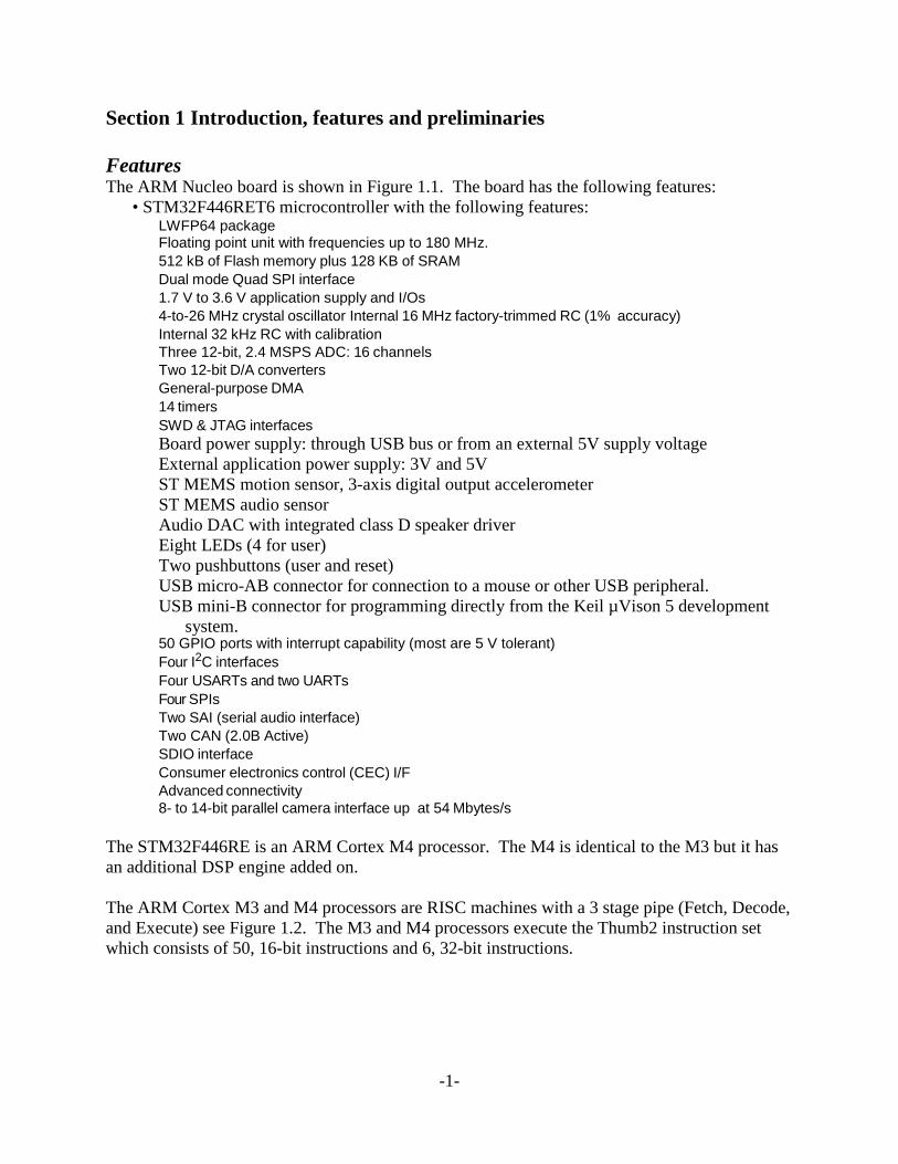
Section 1 Introduction, features and preliminaries Features The ARM Nucleo board is shown in Figure 1.1. The board has the following features:
• STM32F446RET6 microcontroller with the following features: LWFP64 package Floating point unit with frequencies up to 180 MHz. 512 kB of Flash memory plus 128 KB of SRAM Dual mode Quad SPI interface 1.7 V to 3.6 V application supply and I/Os 4-to-26 MHz crystal oscillator Internal 16 MHz factory-trimmed RC (1% accuracy) Internal 32 kHz RC with calibration Three 12-bit, 2.4 MSPS ADC: 16 channels Two 12-bit D/A converters General-purpose DMA 14 timers SWD & JTAG interfaces Board power supply: through USB bus or from an external 5V supply voltage External application power supply: 3V and 5V ST MEMS motion sensor, 3-axis digital output accelerometer ST MEMS audio sensor Audio DAC with integrated class D speaker driver Eight LEDs (4 for user) Two pushbuttons (user and reset) USB micro-AB connector for connection to a mouse or other USB peripheral. USB mini-B connector for programming directly from the Keil µVison 5 development
system. 50 GPIO ports with interrupt capability (most are 5 V tolerant) Four I2C interfaces Four USARTs and two UARTs Four SPIs Two SAI (serial audio interface) Two CAN (2.0B Active) SDIO interface Consumer electronics control (CEC) I/F Advanced connectivity 8- to 14-bit parallel camera interface up at 54 Mbytes/s
The STM32F446RE is an ARM Cortex M4 processor. The M4 is identical to the M3 but it has an additional DSP engine added on. The ARM Cortex M3 and M4 processors are RISC machines with a 3 stage pipe (Fetch, Decode, and Execute) see Figure 1.2. The M3 and M4 processors execute the Thumb2 instruction set which consists of 50, 16-bit instructions and 6, 32-bit instructions.

-2-
Figure 1.1 The ARM Nucleo board. The USB port at the top of the board (mini-B) is the programming port.[3]

-3-
Figure 1.2 The ARM Cortex M3, M4 pipeline. [4]
-4-
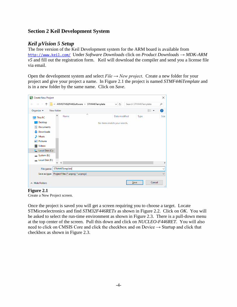
Section 2 Keil Development System Keil µVision 5 Setup The free version of the Keil Development system for the ARM board is available from http://www.keil.com/ Under Software Downloads click on Product Downloads → MDK-ARM v5 and fill out the registration form. Keil will download the compiler and send you a license file via email. Open the development system and select File → New project. Create a new folder for your project and give your project a name. In Figure 2.1 the project is named STMF446Template and is in a new folder by the same name. Click on Save.
Figure 2.1 Create a New Project screen. Once the project is saved you will get a screen requiring you to choose a target. Locate STMicroelectronics and find STM32F446RETx as shown in Figure 2.2. Click on OK. You will be asked to select the run-time environment as shown in Figure 2.3. There is a pull-down menu at the top center of the screen. Pull this down and click on NUCLEO-F446RET. You will also need to click on CMSIS Core and click the checkbox and on Device → Startup and click that checkbox as shown in Figure 2.3.

-5-
Figure 2.2 Select STM32F446RETx for the target device.
Figure 2.3 Selecting the run-time environment. Click on the pull-down menu and select NUCLEO-F446RE. Click on CMSIS Core and click the checkbox and on Device → Startup and click that checkbox. Then click OK. This completes the setup of an empty project. The next step adds the necessary files to the project. You will need to add two files to your project. A) You main c-code file B) A supporting dot-h file named stm32f446.h.

-6-
To add your main c-code, in Keil, click on File→New. This will create a file in Keil on a tab named Text1. Click on File→Save as and save this file as STMF446Template.c. You can name it whatever you want but you need to use a dot c extension. The file stm32f446.h is available on the class website. Download it and place it in the project folder. The files we need are in the project directory but they have not been added to the project. To do this right click on Source Group 1 (under Target) and select Add Existing Files to Source Group 1 (See Figure 2.4) Select the c-code file and click on Add. It's not necessary to add the dot-h file – the c-code which uses it will find it in the directory (you can add it if you want). If you have done this successfully you can expand the source group in the project window and see the files that are in the project. This should look like that shown in Figure 2.5.
Figure 2.4 Add files to source group 1
Figure 2.5 The project column with the files added to the project. Note that the DSP libraries are not needed for EE 354.

-7-
At this point we are ready to enter the c-code for the project. Click on the tab for your c-code. In this example the tab is titled stmf446Template.c. Enter the following program. #include "stm32f446.h" /*stm446Template.c July 1, 2017 This program toggles a bit on PA7 as fast as possible */ int main() {int tmp; //Clock bits RCC_AHB1ENR |= 1; //Bit 0 is GPIOA clock enable bit //I/O bits GPIOA_MODER |= 0x4000; //Bits 15-14 = 01 for digital output on PA7 //OTYPER register resets to 0 so it is push/pull by default GPIOA_OSPEEDER |= 0xC000; //Bits 15-14 = 11 for high speed on PA7 //PUPDR defaults to no pull up no pull down //Main program loop tmp = 0; while(1) {GPIOA_ODR = tmp; //Only PA7 is set up for output so other bits tmp = ~tmp; // have no effect. } } After entering the c-code click on Project→Build Target to save and compile your code. If you have been living a virtuous life your code will compile with no errors and no warnings. (You may get a warning about needing a blank line as the last line in the code. This means a blank line with no spaces. You can add it or just ignore the warning.) You are now ready to load the project code onto the Nucleo board or to do a simulation. The simulation is a software simulation and no board is needed. It has some limitations in that all of the peripherals are not simulated but you can at least see what is in the registers and the memory including the I/O ports. Debugging on the board includes loading and running the code on the Nucleo board via a USB cable. It is often easier to track down a hardware problem by running the code on the board itself. The set up loading the project on the Nucleo board is rather involved but you only need to do it once. We will do the simulation set up first – it is easy. Using the Simulator The simulator is all software based so it needs to know in advance what memory you are using. This is done by creating an initialization file which typically has a .ini extension but is otherwise a simple text file. After you have compiled your program successfully, click on file → new. The μVision environment will open a new file for you. Enter a mapping function given by MAP 0x40000000, 0x40028000 READ WRITE Save the file with the name Debug.ini. See Figure 2.6.

-8-
Figure 2.6 The Debug.ini file. This allows the simulator to read and write to simulated memory at 0x40000000 to 0x40028000 which covers most of the memory area where the processor maps its I/O ports. After creating Debug.ini and saving it, right click on Target1 in the project window and select Options for Target 1. In the screen that appears select the Debug tab as shown in Figure 2.7.
Figure 2.7 Right click on Target 1 in the Project window and select Options for Target 1. Select the Debug tab to get this screen. Click on the "Use Simulator" radio button and browse to the debug.ini file for the Initialization File. In Figure 2.7 select "Use Simulator" and on the left side panel click on the box with three dots (…) in the Initialization file. This will allow you to browse out to locate the Debug.ini file you created earlier. When you select Debug.ini the Initialization file window will look like that shown in Figure 2.7. Click on OK and we are ready to do our simulation. Click on Debug → Start/Stop Debug Session or click on the red button at the top of the screen:

-9-
When you start the debugger you will get a message saying that you are in the "Evaluation mode" with a code size limit of 32K. If you are using the professional version of μVision 5 this message will not appear. For this class the student version is adequate for all assignments. Figure 2.8 shows the debugger screen for this project.
Figure 2.8 The initial debugger screen. If your debugger screen does not have all of these components you can use the view menu to get them. The program that we are debugging uses port A for output. This is called GPIOA (General Purpose I/O port A). Click on Peripherals → System Viewer → GPIOA to show the registers in GPIO port A. See Figure 2.9
Figure 2.9 The registers in GPIOA as seen in the debugger. Click on the + sign to expand the register to see the bits.

-10-
Figure 2.10 Menu buttons for controlling the debugger. These are located on the Debug Toolbar at the top of the screen. If these are not present on your screen you can find them on the view menu. To run the program and do the simulation click on the Run button on the Debug Toolbar. (See Figure 2.10). For this program you will see the Output Data Register (ODR) on GPIOA change from FFFFFFFF to 00000000 since the program writes all ones and all zeros to the port continuously. Notice also that at the bottom of the Register window the number of simulated seconds is also changing. (This time will not be accurately simulated unless you have correctly set the crystal speed before you entered the debugger. To do this right click on Target 1 in the Project windows and select Options for Target 1. Choose the Target tab and set the crystal speed to match that on your board.) You can stop the program at any point by pushing the stop button on the Debug Toolbar. You can also single step through your program using the Step into button. You can stop debugging and go back to the main program screen by clicking on Debug → Start/Stop Debugging.
If while debugging you find an error it is tempting to change the code in the debugger to fix the problem. Such changes will not be effective. If you make any changes to the code they
will not go into effect until you have again recompiled the program. Loading the project on the Nucleo Board 1. You will need a USB cable that has a Type A/mini-B connector for the board and a standard USB connector to plug into your computer. This is the same cable that you use to charge your phone. This USB cable plugs into CN1 on the Nucleo board. If your computer does not locate the driver you will have to locate the driver and install it. The driver is at c:\Keil\ARM\STLink\USBDriver if you need it. If after installing the USB driver you may also need the upgrade utility which is at c:\Keil\ARM\STLink. 2. With your board plugged in we will need to change the project options to use STLink. Click once on Target in the project pane and then click on Project→Options for Target 1 or click or Alt → F7 . Under the Target tab set the crystal speed to 8.0 MHz 3. Under the Debug tab click on the pull down menu on the right and choose STLink Debugger. Also click on the radio button labeled Use so that the Use Simulator button is not chosen. See Figure 2.11.
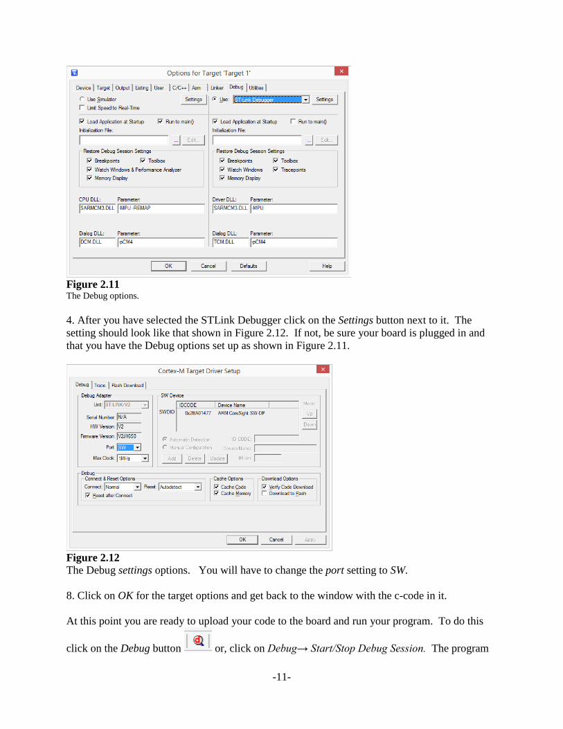
-11-
Figure 2.11 The Debug options. 4. After you have selected the STLink Debugger click on the Settings button next to it. The setting should look like that shown in Figure 2.12. If not, be sure your board is plugged in and that you have the Debug options set up as shown in Figure 2.11.
Figure 2.12 The Debug settings options. You will have to change the port setting to SW. 8. Click on OK for the target options and get back to the window with the c-code in it. At this point you are ready to upload your code to the board and run your program. To do this
click on the Debug button or, click on Debug→ Start/Stop Debug Session. The program

-12-
will be downloaded to your board. Click on Debug→Run to start the program running. With an oscilloscope you will see a square wave at about 1.33 MHz. You can alter the code by adding an empty delay loop like this: int main() {int i, tmp; //Clock bits RCC_AHB1ENR |= 1; //Bit 0 is GPIOA clock enable bit //I/O bits GPIOA_MODER |= 0x4000; //Bits 15-14 = 01 for digital output on PA7 //OTYPER register resets to 0 so it is push/pull by default GPIOA_OSPEEDER |= 0xC000; //Bits 15-14 = 11 for high speed on PA7 //PUPDR defaults to no pull up no pull down //Main program loop tmp = 0; while(1) {GPIOA_ODR = tmp; //Only PA7 is set up for output so other bits tmp = ~tmp; // have no effect. for(i=0;i<10000;i++); //Empty for loop for time delay } } In this case the square wave on PA7 runs at about 160 Hz. For future projects, in order not to have to run through the tedious STLink set up, you can create a new project folder on your computer and download STM446Template.zip to that folder. Unzip the project and delete the main c-file (named STM446Template.c). Open the project by double clicking on STM446Template.uvproj, add you own c-code to the file, and run it as usual.

-13-
Section 3 Quirks, clocks, and details Naming Conventions STMicroelectronics uses the naming convention shown in Figure 3.1 for microcontrollers in this series.
Figure 3.1 Part naming conventions[5]
Architectural Features and Quirks In order to get a microcontroller to run at 180 MHz using relatively slow flash memory it is necessary to have some architectural creativity. For the STM32 M3 and M4 processors this includes a phase locked loop, an Adaptive Real-Time (ART) memory accelerator, and a Multi-Advanced High-speed Bus (AHB) switching Matrix. All of these things run from a rather complex system clock. The following discussion gives an overview of how this works.

-14-
System Clock The STM32 has four clock lines from three sources which can be used to provide the system clock. The sources are: the High-Speed External (HSE) oscillator, the High-Speed Internal (HIS) Oscillator, or the Phase Locked Loop clock (PLL). The HSE clock is driven by an external oscillator. This allows several processors to run from a single external clock. The HSI clock is driven by a 16 MHz internal RC oscillator. Its frequency is approximate but may be calibrated by the user. The PLL can by driven by an external crystal or by the HSI clock. An external 8 MHz crystal can be used by the PLL to provide a 180 MHz internal system clock. In addition to driving the system clock the PLL also provides a second output at 48 MHz to drive the USB and a third output to drive I2S1 and I2S2 clocks for serial communication. The HSE clock can be driven by an external crystal or from an external clock signal. On the Discovery board the HSE oscillator has an 8 MHz external crystal. The HSE clock can be used to drive the Phase-Locked Loop to get an internal clock to 168 MHz. The HSI clock is driven from an internal RC oscillator and runs at approximately 16 MHz. There is also a Low-Speed Internal (LSI) clock which runs from an internal RC oscillator at 32.768 KHz. It is typically used to drive a watchdog timer that runs independently from the system clock. If the 32.768 KHz from the RC oscillator is not precise enough for real-time application the LSE clock can be used with an external crystal. Figure 3.2 shows the clock logic diagram. Note that by default the Nucleo board uses the internal 16 MHz RC circuit for an oscillator. To run at the rated 180 MHz it is necessary to phase lock loop and clock control registers.
Peripheral Clock The peripheral clock for the GPIO ports, the A/D and D/A converters, the timers, and the high speed busses are derived from the system clock by way of a pre-scaler which can be modified by the user. Several pre-scalers are used to configure the Advanced High-speed Bus (AHB) frequency, the Advanced Peripheral Busses: high-speed APB (APB2) and low-speed APB (APB1). The maximum frequency of the AHB is 180 MHz. The maximum allowed frequency of the high-speed APB2 is 90 MHz. The maximum allowed frequency of the low-speed APB1 is 45 MHz. When the processor resets the system clock is set to the 16 MHz internal RC oscillator and the bus pre-scalers are all set to "no scaling" so that APB2, APB1, and AHB all run at 16 MHz. Barrel Shifter A barrel shifter is a combinational logic block which uses multiplexors to shift bit positions as data is copied from one location to another. For a normal shift register it takes n clock cycles to shift n places left or right. The barrel shifter on the Cortex-M4 makes it possible to do up to a 32-bit shift left or right in a single clock cycle.

-15-
Figure 3.2 Clock generation for the STM32 processor[1].

-16-
Phase Locked Loop Internally the STM version of the ARM Cortex M4 processor runs at 180 MHz which is a cycle time of just 5.556 nsec. This would imply that a very fast external interface bus would be needed to communicate with the outside world. For many embedded controller systems this high speed interface is unnecessary. The solution to this problem is to add a phase locked loop into the hardware which allows the CPU to run at 180 MHz and to simultaneously communicate with a synchronized 8 MHz system on the outside. Thus, the STM32F446 requires only an 8 MHz crystal and from the outside, the user sees it as an 8 MHz system although inside it is actually executing instructions at 180 MHz. A system diagram for a phase locked loop (PLL) is shown below. An 8 MHz crystal oscillator runs the external system busses and clocks. Internally a voltage controlled oscillator runs at about 180 MHz. Figure 3.3 shows how this is done. The 8 MHz oscillator is first divided by 8 to get a stable 1 MHz clock. The 1 MHz clock from the crystal is compared to the 1 MHz signal from the divided voltage controlled oscillator. The error signal is fed back to adjust the frequency of the VCO. Effectively, the PLL acts as a frequency multiplier.
Figure 3.3 System diagram for a phase locked loop. Flash Memory access Flash memory has a read access time of a few tens of nano-seconds per byte after the first byte. For a processor running with a clock period of about 6 nano-seconds this is much too slow. An obvious solution is to add an SRAM cache memory to the chip. This means that the instructions in the flash memory would be loaded into the cache before being delivered to the processor. Since the data is present on the chip is in two places and the cache requires some considerable hardware overhead for its operation this is inefficient. Instead of adding a cache, the STM32 organizes the flash memory into 128-bit words. Each access produces a single 128-bit word which can consist of eight 16-bit Thumb instructions. Organizing the flash memory into 128-bit words effectively speeds up the access time by a factor of 8 for Thumb instruction access. However, is a conditional branch is taken, the next instruction in the 128-bit word may not be the one that is needed. To address this problem the STM32 has an Advanced Real-Time (ART) accelerator module which can store sixty-four 128 bit sequences. Each time a branch occurs the instructions at the target location are saved in the
-17-
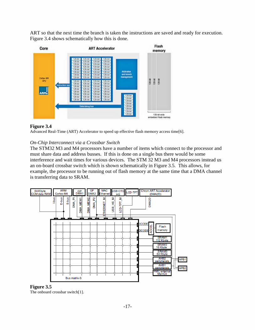
ART so that the next time the branch is taken the instructions are saved and ready for execution. Figure 3.4 shows schematically how this is done.
Figure 3.4 Advanced Real-Time (ART) Accelerator to speed up effective flash memory access time[6]. On-Chip Interconnect via a Crossbar Switch The STM32 M3 and M4 processors have a number of items which connect to the processor and must share data and address busses. If this is done on a single bus there would be some interference and wait times for various devices. The STM 32 M3 and M4 processors instead us an on-board crossbar switch which is shown schematically in Figure 3.5. This allows, for example, the processor to be running out of flash memory at the same time that a DMA channel is transferring data to SRAM.
Figure 3.5 The onboard crossbar switch[1].

-18-
Processor Block Diagram A block diagram of the STM32F446RET6 processor is shown in Figure 3.6. For the Nucleo board the STM32F446RET6 has 512 KB of flash memory and 128 K of RAM.
Figure 3.6 Block diagram of STM32F446RET6 processor.[5]

-19-
Section 4 Programming Details Assembly Language Programmer's Model Figure 4.1 shows the internal registers accessible to the assembly language programmer. The top three registers have special functions: R13 is the stack pointer; R14 is the link register; R15 is the program counter.
Figure 4.1 Assembly language programmer's model[7]. The normal 32-bit ARM instruction can access all of the registers. The Thumb and most of the Thumb2 instructions are only 16-bit instructions and have access only to R0-R7 as general purpose registers. For the Thumb instructions only the MOV instruction has access to all of the general purpose registers. The link register R14 is a special one-level stack. When a subprogram call is made from a main program the return address goes into R14. If the subprogram makes further calls the return address goes onto the stack in memory. The assembly language instruction BLX (Branch and Link) automatically uses this register. Register R13 is the stack pointer. The lower two bits of this register is always zero since it accesses the stack on 32-bit word boundaries. Normal operations always use SP_main but for thread mode the processor can be configured to use SP_process. Register R15 is the program counter. It is 32-bits long and there is a linear address space from 0 to 232-1. Bit 0 of this register is always 0 so that instructions are aligned on 16-bit boundaries.

-20-
The CPU flags are stored in the program status register. There are three program status registers called Application Program Status Register (APSR), Interrupt Program Status Register (IPSR), and the Execution Program Status Register (EPSR). These three status registers have mutually exclusive bit fields and can be combined and read as a single register called the Program Status Register (PSR). Figure 4.2 shows these registers.
Figure 4.2 The three program status registers can be read a single register called PSR with bit fields as shown2. Bits 27 to 31 are the condition codes or CPU flags. The definition for these is shown in Figure 4.3.
Figure 4.3 Definition of the condition code bits[2]. In addition to the normal CPU flags in Figure 4.3, the Program Status Register has three other fields with status information. These are the Greater than or Equal (GE) field, the Interrupt Continuable/If Then (ICI/IT) field, and the Interrupt Service Routine (ISR) number. The GE field holds information that can be used by the SEL and SIMD assembly language instruction for

-21-
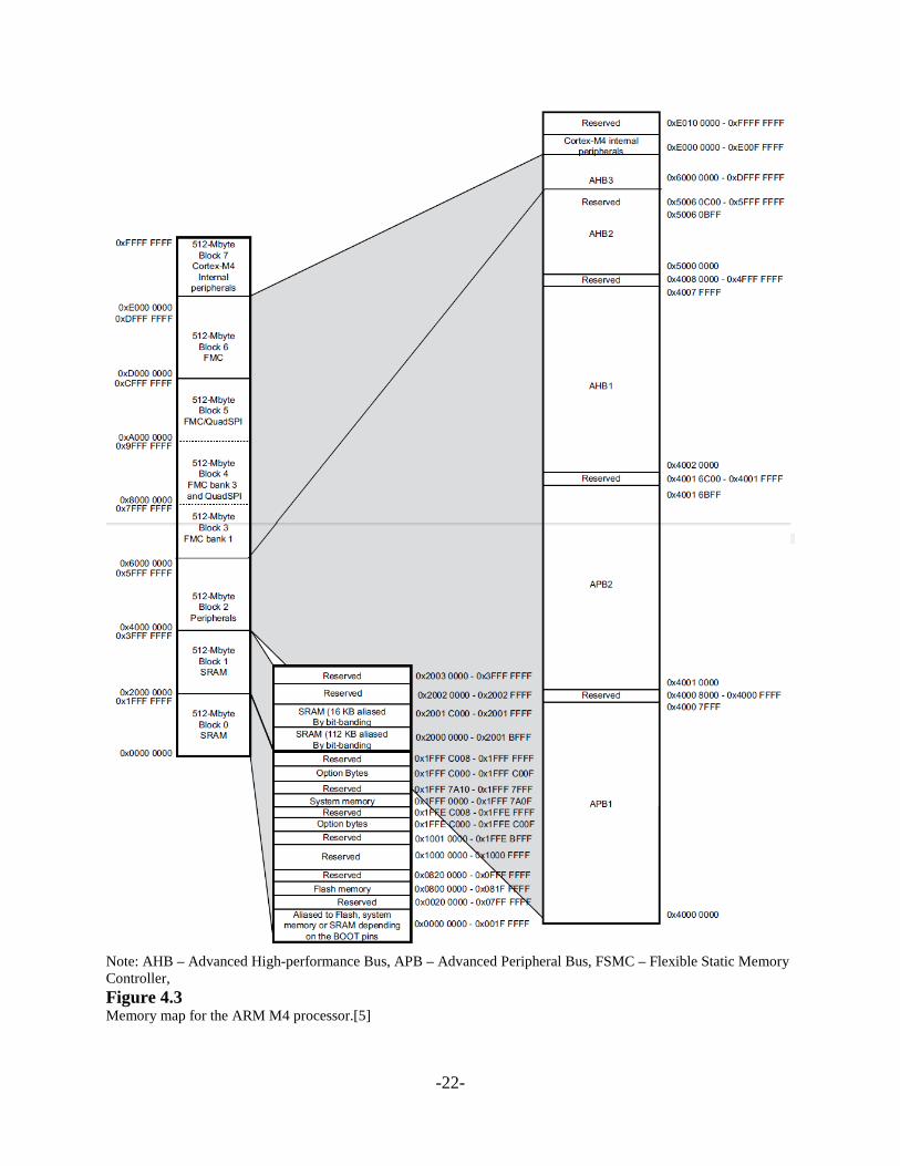
certain conditions. See [8] pp. 95-96. The ICI/IT field holds information for conditional execution (if-then) assembly language instructions. The ISR number field holds the exception number currently being executed. Memory Mapping The ARM has a 32-bit address and in hex addresses range from 0000 0000 to FFFF FFFF. This is a linear address space and there are no I/O instructions since all ports are mapped from memory. Figure 4.3 gives an overview of the memory mapping. Refer to the User's manual for the address of specific peripheral registers. Memory map details All of the I/O ports are mapped into the 4 GByte memory space. From Figure 4.3 we see that the peripherals are mapped to the address range 0x4000 0000 to 0x5FFF FFFF. Table 1 gives the addresses of the most common registers for the I/O devices. This list is incomplete. See Table 1 in the STM32 Reference Manual [1] for a more complete list of register boundary addresses and links to specific register addresses. Addresses for the interrupt system are not in the Reference Manual. You can find these in the Programmer's Manual [2].
-22-
Note: AHB – Advanced High-performance Bus, APB – Advanced Peripheral Bus, FSMC – Flexible Static Memory Controller, Figure 4.3 Memory map for the ARM M4 processor.[5]
-23-
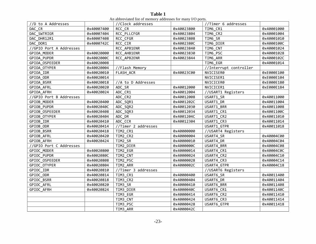
Table 1 An abbreviated list of memory addresses for many I/O ports.
//D to A Addresses //Clock addresses //Timer 6 addresses DAC_CR 0x40007400 RCC_CR 0x40023800 TIM6_CR1 0x40001000 DAC_SWTRIGR 0x40007404 RCC_PLLCFGR 0x40023804 TIM6_CR2 0x40001004 DAC_DHR12R1 0x40007408 RCC_CFGR 0x40023808 TIM6_SR 0x40001010 DAC_DOR1 0x4000742C RCC_CIR 0x4002380C TIM6_DIER 0x4000100C //GPIO Port A Addresses RCC_APB1ENR 0x40023840 TIM6_CNT 0x40001024 GPIOA_MODER 0x40020000 RCC_AHB1ENR 0x40023830 TIM6_PSC 0x40001028 GPIOA_PUPDR 0x4002000C RCC_APB2ENR 0x40023844 TIM6_ARR 0x4000102C GPIOA_OSPEEDER 0x40020008 TIM6_EGR 0x40001014 GPIOA_OTYPER 0x40020004 //Flash Memory //Interrupt controller GPIOA_IDR 0x40020010 FLASH_ACR 0x40023C00 NVICISER0 0xE000E100 GPIOA_ODR 0x40020014 NVICISER1 0xE000E104 GPIOA_BSRR 0x40020018 //A to D Addresses NVICICER0 0xE000E180 GPIOA_AFRL 0x40020020 ADC_SR 0x40012000 NVICICER1 0xE000E184 GPIOA_AFRH 0x40020024 ADC_CR1 0x40012004 //USART1 Registers //GPIO Port B Addresses ADC_CR2 0x40012008 USART1_SR 0x40011000 GPIOB_MODER 0x40020400 ADC_SQR1 0x4001202C USART1_DR 0x40011004 GPIOB_PUPDR 0x4002040C ADC_SQR2 0x40012030 USART1_BRR 0x40011008 GPIOB_OSPEEDER 0x40020408 ADC_SQR3 0x40012034 USART1_CR1 0x4001100C GPIOB_OTYPER 0x40020404 ADC_DR 0x4001204C USART1_CR2 0x40011010 GPIOB_IDR 0x40020410 ADC_CCR 0x40012304 USART1_CR3 0x40011014 GPIOB_ODR 0x40020414 //Timer 2 addresses USART1_GTPR 0x40011018 GPIOB_BSRR 0x40020418 TIM2_CR1 0x40000000 //USART4 Registers GPIOB_AFRL 0x40020420 TIM2_CR2 0x40000004 USART4_SR 0x40004C00 GPIOB_AFRH 0x40020424 TIM2_SR 0x40000010 USART4_DR 0x40004C04 //GPIO Port C Addresses TIM2_DIER 0x4000000C USART4_BRR 0x40004C08 GPIOC_MODER 0x40020800 TIM2_EGR 0x40000014 USART4_CR1 0x40004C0C GPIOC_PUPDR 0x4002080C TIM2_CNT 0x40000024 USART4_CR2 0x40004C10 GPIOC_OSPEEDER 0x40020808 TIM2_PSC 0x40000028 USART4_CR3 0x40004C14 GPIOC_OTYPER 0x40020804 TIM2_ARR 0x4000002C USART4_GTPR 0x40004C18 GPIOC_IDR 0x40020810 //Timer 3 addresses //USART6 Registers GPIOC_ODR 0x40020814 TIM3_CR1 0x40000400 USART6_SR 0x40011400 GPIOC_BSRR 0x40020818 TIM3_CR2 0x40000404 USART6_DR 0x40011404 GPIOC_AFRL 0x40020820 TIM3_SR 0x40000410 USART6_BRR 0x40011408 GPIOC_AFRH 0x40020824 TIM3_DIER 0x4000040C USART6_CR1 0x4001140C TIM3_EGR 0x40000414 USART6_CR2 0x40011410 TIM3_CNT 0x40000424 USART6_CR3 0x40011414 TIM3_PSC 0x40000428 USART6_GTPR 0x40011418 TIM3_ARR 0x4000042C

-24-
Pin Assignments The microcontroller on the Nucleo board is the STM32F446RET6 which comes in a 64 pin LQFP 64 (Low profile Quad Flat Pack) package. The pin assignments are shown in Figure 4.4.
Figure 4.4. The STM32F446RET6 IC Package with assigned pins[5]
The Nucleo board has two connectors each consisting of two columns of pins. Connector CN7 is on the left in Figure 1.1 and CN10 is on the right. CN7 and CN10 each have 38 pins in two 19-pin columns for a total of 76 pins so that all pins of the LQFP 64 package are brought out along with multiple power and ground lines. A few pins have no connection (NC). See Table 29 in the User's Manual for a complete mapping of all of the package pins to the board pins at CN7 and CN10. For the I/O ports, Table 2 gives the pins are available for the Nucleo Board:

-25-
Table 2 Pins available on Nucleo Board
Port Pins on Nucleo Board PA PA0 to PA15
PB PB0 to PB10 plus PB12 to PB15 PC PC0 to PC15 PD PD2 PE None PF None PG None PH PH0-PH1 PI None
Notes: 1. PB11 is not brought out to a board pin. 2. PA13 and PA14 are shared with the debug circuitry and should be avoided if possible. 3. A User LED (green) is connected to PA5 and is on when the pin is high. 4. A User push-button is connected to PC13. GPIO Pins Each of the GPIO ports on the ARM Cortex M4 processor has ten 32-bit registers that are used to configure the port and get information in and out. Table 3 defines these registers.
Table 3 GPIO Port control and information registers
Reg name Function Comment GPIOx_MODER Mode register Input, output, alternate function1, or analog GPIOx_OTYPER Type register Allows push/pull or open drain GPIOx_OSPEEDR Speed register Allows low, medium, fast or high speed GPIOx_PUPDR Pull up/Pull down register Allows pull up, pull down, or no pull up or
pull down GPIOx_IDR Input data register Stores data for reading from outside GPIOx_ODR Output data register Stores data for writing to outside GPIOx_BSRR Bit Set/Reset register Writing a 1 to a bit in this register allows the
user to set or reset a bit in the ODR GPIOx_LCKR Lock register Allows the user to lock a pin so that its value
cannot be changed. GPIOx_AFRH Alt function register high GPIOx_AFRL Alt function register low
Note 1: alternate function include timers, UARTs, CAN, Ethernet, I2C, and SPI to be attached to a port pin. Figure 4.5 shows a schematic of the typical I/O pin circuity.

-26-
Figure 4.5 Typical electrical diagram for a GPIO pin [1]. Notice that on the output control there is a P-MOS/N-MOS push pull circuit which can be turned on or off using the OTYPER register. There is also a pull up/pull down configuration on the I/O line at the pin. This is set up by the PUPDR register. The protection diodes allow all of the I/O pins to be 5 volt tolerant. The input has a Schmitt trigger which is bypassed for analog input. Each GPIO pin can source or sink up to 25 ma [5]. However, care must be taken so that the total current going into or out of the chip does not exceed 120 ma. Exceeding this value may result in overheating. Addressing ports – Include files Assembly code The ARM processor is mostly a RISC machine with a load and store architecture. Since all of the ports are memory mapped, reading/writing to a port is the same as reading/writing to a memory location. For example the following assembly code reads GPIOA to a register: ;From Table 1 the address of GPIOA_ODR is 0x40020014 ldr r4, =0x40020014; address of Port A ldr r3, [r4]; Copy port to r3 To copy data to GPIOA we could use the following: ldr r4, =0x40020014; address of Port A str r3, [r4]; Store r3 in port A Notice that the load instruction has data flowing from right to left but the store instruction has data flowing from left to right. In both cases, the square brackets around r4 indicate that it holds a register indirect address.

-27-
C-Code traditional style In traditional C-code we create an include file which allows us to define register names for the register memory addresses. Typical define statements in such an include file for the GPIOA input and output data registers might look like this: #define GPIOA_IDR (*((volatile unsigned long *) 0x40020010)) //GPIO A Input Data reg #define GPIOA_ODR (*((volatile unsigned long *) 0x40020014)) //GPIO A Output Data reg In the line for GPIOA_IDR the code (volatile unsigned long *) 0x40020010 Does a cast making the hexadecimal number 0x40020010 a pointer type. The * in front of this dereferences this pointer allowing us to get the data that address. In C-code we can write: GPIOA_ODR |= 0x00000080; //Make bit 7 a 1 OR we could write: GPIOA_ODR |= (1 << 7); //Also makes bit 7 a 1 The file stm32f446.h is an include file which has most of the registers for the ARM Cortex defined in this manner. This file is available in the template program for the Keil V5 programming environment on the course web site. C-Code CMSIS style The Cortex Microcontroller Software Interface System (CMSIS) is a standardized, vendor independent software interface for the Cortex M-series processors. In addition to a number of libraries to interface code to peripherals, it provides register definitions that allow access by way of c-code. These register definitions make use of the typedef structure and pointers and provides a uniform access path for the peripherals and registers on all of the ARM Cortex processors. In c-code the typedef statement allows the user to rename a variable type. For example I can enter: typdef int weight; //Rename int to weight weight w1, w2; //Declare w1 and w2 as ints You can extend this to arrays. For example typedef float height[50]; //Rename float as an array named height height men; //Create men[50] as floats The typedef declaration can also be used with the struct declaration. Consider this example: typedef struct //rename a struct as record {int age; float height; float weight; } record; record john, mary; //john and mary are now structs The user has access to the variables in the struct by means of the dot operator. john.age = 22;
-28-
If we look at the include files for the ARM processor using CMSIS we find definitions for structs that might look like the following: /*!< Peripheral memory map */ #define PERIPH_BASE ((uint32_t)0x40000000) #define APB1PERIPH_BASE PERIPH_BASE #define APB2PERIPH_BASE (PERIPH_BASE + 0x00010000) #define AHB1PERIPH_BASE (PERIPH_BASE + 0x00020000) #define AHB2PERIPH_BASE (PERIPH_BASE + 0x10000000) /*!< AHB1 peripherals */ #define GPIOA_BASE (AHB1PERIPH_BASE + 0x0000) #define GPIOB_BASE (AHB1PERIPH_BASE + 0x0400) #define GPIOC_BASE (AHB1PERIPH_BASE + 0x0800) #define GPIOD_BASE (AHB1PERIPH_BASE + 0x0C00) #define GPIOE_BASE (AHB1PERIPH_BASE + 0x1000) #define GPIOF_BASE (AHB1PERIPH_BASE + 0x1400) #define GPIOG_BASE (AHB1PERIPH_BASE + 0x1800) #define GPIOH_BASE (AHB1PERIPH_BASE + 0x1C00) #define GPIOI_BASE (AHB1PERIPH_BASE + 0x2000) From these declarations we see that, for example, the GPIOA_BASE address is at 0x40020000 and GPIOG_BASE is at 0x40021800. A typedef for a struct is defined to gain access to the port registers. typedef struct { __IO uint32_t MODER; //Address offset: 0x00 __IO uint32_t OTYPER; //Address offset: 0x04 __IO uint32_t OSPEEDR; //Address offset: 0x08 __IO uint32_t PUPDR; //Address offset: 0x0C __IO uint32_t IDR; //Address offset: 0x10 __IO uint32_t ODR; //Address offset: 0x14 __IO uint32_t BSRR; //Address offset: 0x18 __IO uint32_t LCKR; //Address offset: 0x1C __IO uint32_t AFR[2]; //Address offset: 0x20-0x24 */ } GPIO_TypeDef; Finally we can define the individual port pointers. #define GPIOA ((GPIO_TypeDef *) GPIOA_BASE) #define GPIOB ((GPIO_TypeDef *) GPIOB_BASE) #define GPIOC ((GPIO_TypeDef *) GPIOC_BASE) #define GPIOD ((GPIO_TypeDef *) GPIOD_BASE) #define GPIOE ((GPIO_TypeDef *) GPIOE_BASE) #define GPIOF ((GPIO_TypeDef *) GPIOF_BASE) #define GPIOG ((GPIO_TypeDef *) GPIOG_BASE) #define GPIOH ((GPIO_TypeDef *) GPIOH_BASE)

-29-
#define GPIOI ((GPIO_TypeDef *) GPIOI_BASE) We see that (GPIO_TypeDef *) is defining a pointer to struct. For example, after these declaration, GPIOA will be a pointer to GPIOA_BASE which is the base address of the registers associated with GPIOA. To access one of the registers, say the output data register, we can use the following: (*GPIOA).ODR = 0; In this notation the *GPIOA dereferences the pointer and dot operator allows access to a member or the struct. But this is a bit unwieldy so there is a replacement notation. GPIOA -> 0; This notation uses the arrow operator to access a struct member. To summarize the following three lines to the same thing – set bit PA7 to 0 using different notation. The first uses a define statement that makes the address of the output data register on GPIO port A a dereferenced pointer. It uses #include "stm32f446.h" which is an include file from the course web site. The second and third use #include "stm32f446xx.h" which is an include file that comes from the vendor (STM) and is part of the installation of Keil µVision 5 when you use the Nucleo Board. For the second and third the GPIOA term is a pointer to a structure that defines the registers for the port with offsets from a base address. GPIOA_ODR &= ~(1 << 7); //PA7 to 0 GPIOA -> ODR &= ~(1 << 7); //PA7 to 0 (*GPIOA).ODR &= ~(1 << 7); //PA7 to 0 Easy Guide to Assembly Code In general, for the ARM processors you can add an s to an instruction and it will alter the flags. Using the same instruction without an s will not alter the flags. For the compiler/assembler that we have this is often not an option and you are forced to use one or the other. Note also that the assembler is not case sensitive so that R0 is the same as r0 and you can use whatever you want although you should be consistent for readability. This particular assembler is sensitive to spaces. All labels must begin in column 1 and no assembly mnemonic is allowed to begin in that column. Instructions Loading immediate data into a register: ldr R3, =0x000003FF; Loads the 32 bit hex number into R3 ldr R2, =41; Loads 41 base 10 into R2 Store a register into a memory: str R2, [R1]; Stores R2 into the memory whose address is in R1 Copy one register into another:
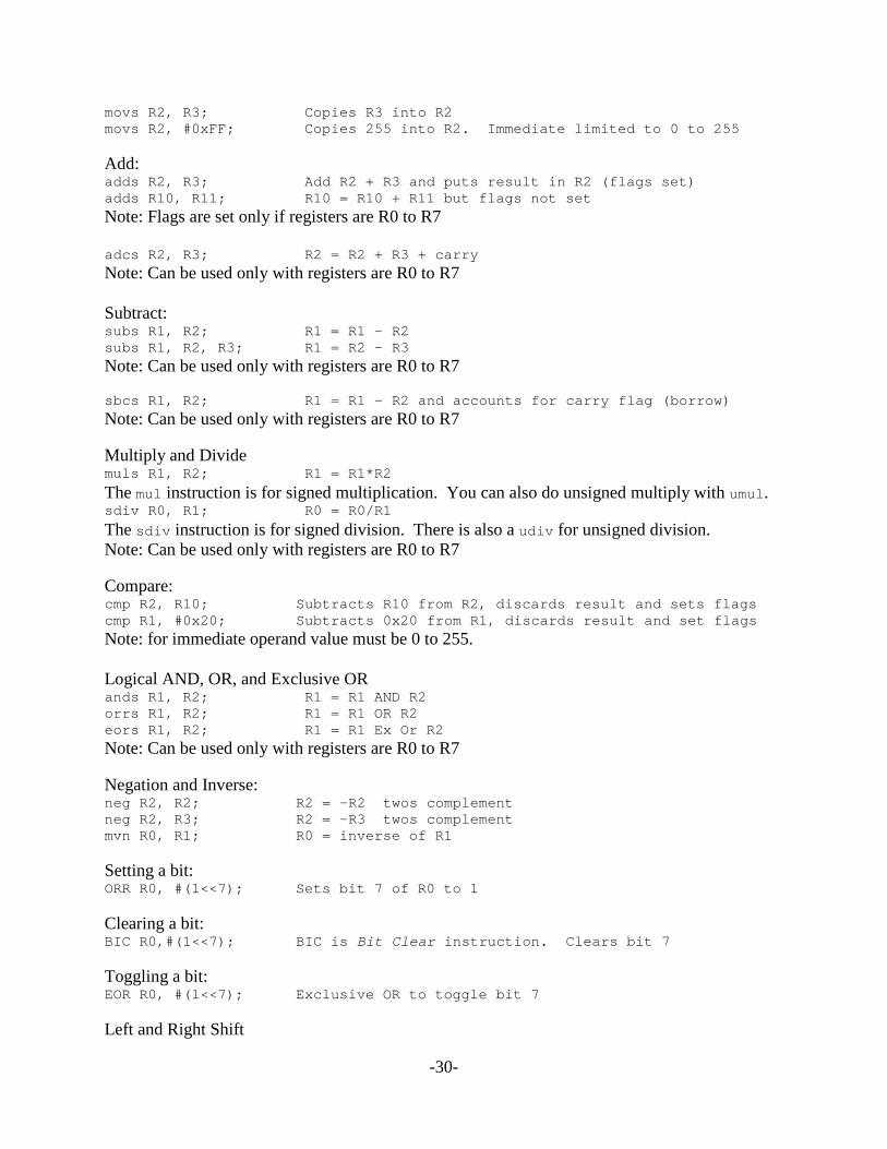
-30-
movs R2, R3; Copies R3 into R2 movs R2, #0xFF; Copies 255 into R2. Immediate limited to 0 to 255 Add: adds R2, R3; Add R2 + R3 and puts result in R2 (flags set) adds R10, R11; R10 = R10 + R11 but flags not set Note: Flags are set only if registers are R0 to R7 adcs R2, R3; R2 = R2 + R3 + carry Note: Can be used only with registers are R0 to R7 Subtract: subs R1, R2; R1 = R1 – R2 subs R1, R2, R3; R1 = R2 – R3 Note: Can be used only with registers are R0 to R7 sbcs R1, R2; R1 = R1 – R2 and accounts for carry flag (borrow) Note: Can be used only with registers are R0 to R7 Multiply and Divide muls R1, R2; R1 = R1*R2 The mul instruction is for signed multiplication. You can also do unsigned multiply with umul. sdiv R0, R1; R0 = R0/R1 The sdiv instruction is for signed division. There is also a udiv for unsigned division. Note: Can be used only with registers are R0 to R7 Compare: cmp R2, R10; Subtracts R10 from R2, discards result and sets flags cmp R1, #0x20; Subtracts 0x20 from R1, discards result and set flags Note: for immediate operand value must be 0 to 255. Logical AND, OR, and Exclusive OR ands R1, R2; R1 = R1 AND R2 orrs R1, R2; R1 = R1 OR R2 eors R1, R2; R1 = R1 Ex Or R2 Note: Can be used only with registers are R0 to R7 Negation and Inverse: neg R2, R2; R2 = -R2 twos complement neg R2, R3; R2 = -R3 twos complement mvn R0, R1; R0 = inverse of R1 Setting a bit: ORR R0, #(1<<7); Sets bit 7 of R0 to 1 Clearing a bit: BIC R0,#(1<<7); BIC is Bit Clear instruction. Clears bit 7 Toggling a bit: EOR R0, #(1<<7); Exclusive OR to toggle bit 7 Left and Right Shift

-31-
lsls R2, R3, #5; shift left R3 5 times and store in R2 lsls R2, R3; shift left R2, R3 value times. If R3 is 31, R2 is cleared, if R3 > 31 R2 and carry are cleared. lsrs R2, R3, #5; shift right R3 5 times and store in R2 lsrs R2, R3; shift right R2, R3 value times. If R3 is 31, R2 is cleared, if R3 > 31 R2 and carry are cleared. asrs R2, R3, #5; arithmetic shift right R3 5 times and store in R2 asrs R2, R3; arithmetic shift right R2, R3 value times. If R3 is 31, R2 is cleared, if R3 > 31 R2 and carry are cleared. Note that because shifting is done with the barrel shifter you can add a shift operation to the second source operand for most instructions. For example: add R1, R0, R0, lsl #3; R1 = R0 + R0 << 3 Branch instructions B Target; unconditional branch to target within ±2K (10 bits) B{Cond} Target; conditional branch to target within -252 to +258 BL{Cond} Target; Branch and link. Stores return address in R14 and conditionally branches to target. To return from subroutine move R14(link reg) into R15(PC) BX {Cond} Rm; Branches indirect to address in Rm. BLX {Cond} Rm; Branches indirect to address in Rm and stores return in R14 (link reg).
Table 4 Condition codes for the branch instructions
Condition Flags Explantion
EQ Z set equal
NE Z clear not equal
CS/HS C set unsigned higher or same
CC/LO C clear unsigned lower
MI N set negative
PL N clear positive or zero
VS V set overflow
VC V clear no overflow
HI C set and Z clear unsigned higher
LS C clear or Z set unsigned lower or same
GE N equals V signed greater or equal
LT N not equal to V signed less than
GT Z clear AND (N equals V) signed greater than
LE Z set OR (N not equal to V) signed less than or equal
AL (ignored) always (usually omitted) Push and Pop push {R1, R2}; Pushes R1 and R2 on the stack push {R1-R5}; Pushes R1, R2, R3, R4, and R5 on the stack

-32-
push {R1, R2, LR}; Pushes R1, R2, and the link register on the stack pop {R1, R2}; Pops R1 and R2 on the stack pop {R1-R5}; Pops R1, R2, R3, R4, and R5 from the stack pop {R1, R2, LR}; Pops R1, R2, and the link register from the stack Note: Can be used only with registers are R0 to R7 and the link register. Calling functions There are no call instructions in ARM assembly language. In place of an explicit call you use the BL instruction which is a Branch and Link. BL branches to the function but it also saves the return address in the link register (r14). To return from a function you use B lr (or BX lr) which branches to the address in the link register. If a function calls another function it must save the link register before doing a branch and link – otherwise the original link will be destroyed. You can do this by pushing the link register on the stack push lr. To return you can pop the link register and do a BX lr or you can simply pop the stack into the program counter. The sequence below shows how to call multiple functions in assembly code: ... bl Sub1 ...
Sub1 ... push lr bl Sub2 pop {pc}
Sub2 ... push lr bl Sub3 pop {pc}
Sub3 ... bx lr
Assembler Directives An assembler directive is a command that tells the assembler what to do with some portion of your program. It is not an executable statement. A complete list of assembler directives is given in Chapter 6 of ARM Assembler Reference [9]. The most commonly used directives are listed in Table 5 along with a brief description of what they do.
Table 5 A list of frequently used ARM assembler directives
Directive Description ALIGN Addresses need to be aligned on a 4-byte boundary. Use ALIGN 4 after a thumb instruction
to ensure four-byte alignment since many thumb instructions are just 2-bytes long. AREA The AREA directive instructs the assembler to assemble a new code or data section. Sections
are independent, named, indivisible chunks of code or data that are manipulated by the linker. For example, AREA Ex1, CODE, READONLY could be used for a new section named Ex1.
DCD DCDU
The DCD directive allocates one or more words of memory, aligned on four-byte boundaries, and defines the initial runtime contents of the memory. & is a synonym for DCD. DCDU is the same, except that the memory alignment is arbitrary.
END This must be used at the end of all assembly code and should appear only once in a module.
ENTRY Declares the entry point of a program
EQU The EQU directive gives a symbolic name to a numeric constant, a register-relative value or a PC-relative value. * is a synonym for EQU. For example Addr1 EQU 0x12345678 allows you to use Addr1 in place of the hex constant in a program.
EXPORT The EXPORT directive declares a symbol that can be used by the linker to resolve symbol references in separate object and library files.
-33-
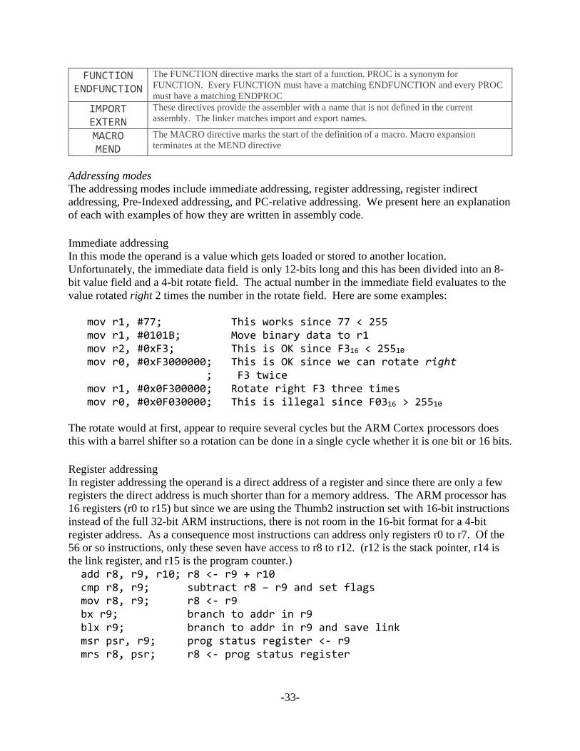
FUNCTION ENDFUNCTION
The FUNCTION directive marks the start of a function. PROC is a synonym for FUNCTION. Every FUNCTION must have a matching ENDFUNCTION and every PROC must have a matching ENDPROC
IMPORT EXTERN
These directives provide the assembler with a name that is not defined in the current assembly. The linker matches import and export names.
MACRO MEND
The MACRO directive marks the start of the definition of a macro. Macro expansion terminates at the MEND directive
Addressing modes The addressing modes include immediate addressing, register addressing, register indirect addressing, Pre-Indexed addressing, and PC-relative addressing. We present here an explanation of each with examples of how they are written in assembly code. Immediate addressing In this mode the operand is a value which gets loaded or stored to another location. Unfortunately, the immediate data field is only 12-bits long and this has been divided into an 8-bit value field and a 4-bit rotate field. The actual number in the immediate field evaluates to the value rotated right 2 times the number in the rotate field. Here are some examples: mov r1, #77; This works since 77 < 255 mov r1, #0101B; Move binary data to r1 mov r2, #0xF3; This is OK since F316 < 25510 mov r0, #0xF3000000; This is OK since we can rotate right ; F3 twice mov r1, #0x0F300000; Rotate right F3 three times mov r0, #0x0F030000; This is illegal since F0316 > 25510 The rotate would at first, appear to require several cycles but the ARM Cortex processors does this with a barrel shifter so a rotation can be done in a single cycle whether it is one bit or 16 bits. Register addressing In register addressing the operand is a direct address of a register and since there are only a few registers the direct address is much shorter than for a memory address. The ARM processor has 16 registers (r0 to r15) but since we are using the Thumb2 instruction set with 16-bit instructions instead of the full 32-bit ARM instructions, there is not room in the 16-bit format for a 4-bit register address. As a consequence most instructions can address only registers r0 to r7. Of the 56 or so instructions, only these seven have access to r8 to r12. (r12 is the stack pointer, r14 is the link register, and r15 is the program counter.) add r8, r9, r10; r8 <- r9 + r10 cmp r8, r9; subtract r8 – r9 and set flags mov r8, r9; r8 <- r9 bx r9; branch to addr in r9 blx r9; branch to addr in r9 and save link msr psr, r9; prog status register <- r9 mrs r8, psr; r8 <- prog status register
-34-
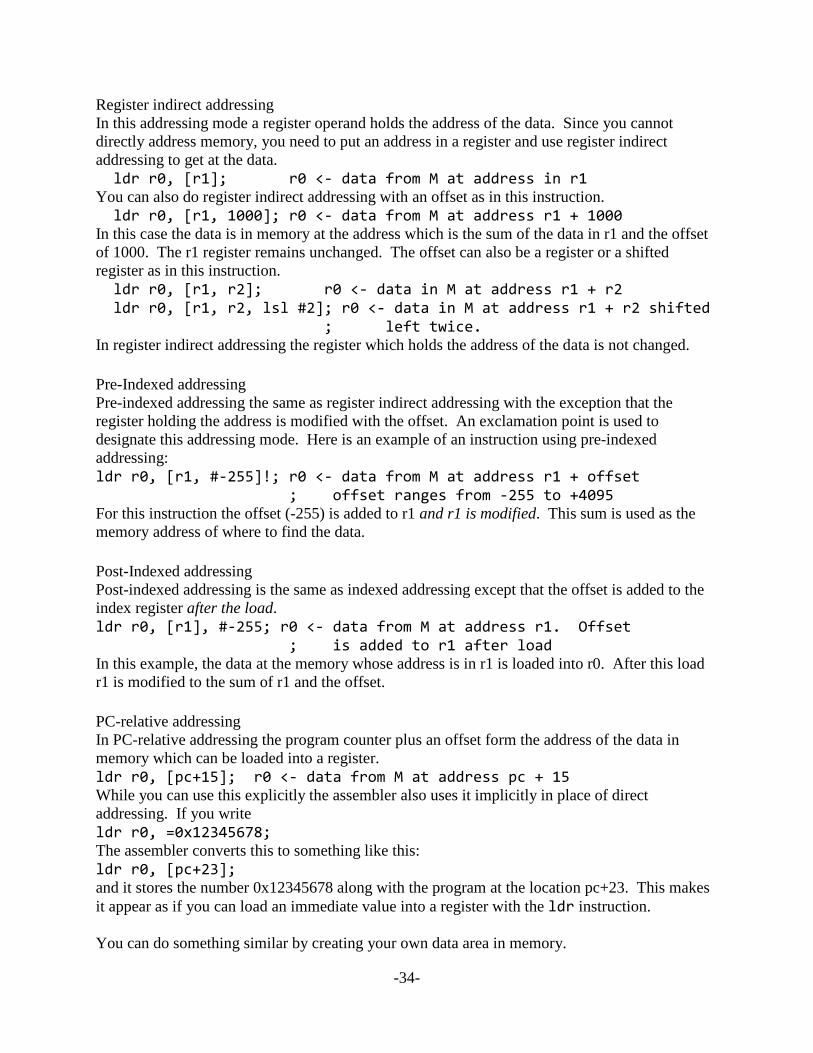
Register indirect addressing In this addressing mode a register operand holds the address of the data. Since you cannot directly address memory, you need to put an address in a register and use register indirect addressing to get at the data. ldr r0, [r1]; r0 <- data from M at address in r1 You can also do register indirect addressing with an offset as in this instruction. ldr r0, [r1, 1000]; r0 <- data from M at address r1 + 1000 In this case the data is in memory at the address which is the sum of the data in r1 and the offset of 1000. The r1 register remains unchanged. The offset can also be a register or a shifted register as in this instruction. ldr r0, [r1, r2]; r0 <- data in M at address r1 + r2 ldr r0, [r1, r2, lsl #2]; r0 <- data in M at address r1 + r2 shifted ; left twice. In register indirect addressing the register which holds the address of the data is not changed. Pre-Indexed addressing Pre-indexed addressing the same as register indirect addressing with the exception that the register holding the address is modified with the offset. An exclamation point is used to designate this addressing mode. Here is an example of an instruction using pre-indexed addressing: ldr r0, [r1, #-255]!; r0 <- data from M at address r1 + offset ; offset ranges from -255 to +4095 For this instruction the offset (-255) is added to r1 and r1 is modified. This sum is used as the memory address of where to find the data. Post-Indexed addressing Post-indexed addressing is the same as indexed addressing except that the offset is added to the index register after the load. ldr r0, [r1], #-255; r0 <- data from M at address r1. Offset ; is added to r1 after load In this example, the data at the memory whose address is in r1 is loaded into r0. After this load r1 is modified to the sum of r1 and the offset. PC-relative addressing In PC-relative addressing the program counter plus an offset form the address of the data in memory which can be loaded into a register. ldr r0, [pc+15]; r0 <- data from M at address pc + 15 While you can use this explicitly the assembler also uses it implicitly in place of direct addressing. If you write ldr r0, =0x12345678; The assembler converts this to something like this: ldr r0, [pc+23]; and it stores the number 0x12345678 along with the program at the location pc+23. This makes it appear as if you can load an immediate value into a register with the ldr instruction. You can do something similar by creating your own data area in memory.

-35-
AsmLoopExmp PROC push {r0-R5}; save the registers ... ldr r0, =Data ldr r1, [r0]; ldr r2, [r0, #4]; ... pop {r0-r5}; Restore the registers bx lr; ENDP Data DCD 0x87654321, 0x45362718 The term DCD is an assembler directive to create storage for a 32-bit word or multiple words. Data is a label at the location of the two words created. The instruction ldr r0, =Data appears to load the address of Data into r0 as an immediate operand. But in fact, the assembler converts this sequence to PC-relative addressing: ldr r0, [pc+24]; where the assembler has calculated that the label Data is 24 bytes ahead of its present location. You could do the same thing by hand but this notation makes it much easier. Programming in Assembly Code There are two methods that can be used to write assembly code in Keil µVision 5. The first is to write a function in assembly code and incorporate that function in a main program written in C. The second is to write the assembly code directly. Writing an Assembler function in a C-Code program To use this method you write a main program in C-code and use the C-code to call the assembler function. You will need to use a function prototype and it can have a return value and a parameter list. The first four parameters are passed in the registers R0, R1, R2, and R3. If there are more than four parameters the remainder are passed on the stack. The return value always comes back in R0. The sample code in Figure 4.6 shows a c-program which called an assembler function called Add2 and passes it two integer parameters. The function adds the two parameters which it catches in R0 and R1 and returns the sum in R0.

-36-
/*AsmAdd2.c April 23, 2016 */ #include "stm32f446.h" __asm int Add2(int x, int y); int main() {int x, y, z; x = 5; y = 7; z = Add2(x, y); } __asm int Add2(int x, int y) { ADD R0, R1; BX LR; return }
Figure 4.6 An assembly function called by a c program. When you enter the program in Figure 4.6 in µVision 5 the error checking does not recognize the assembly code as correct c-syntax and flags all of the assembly code as errors. However, you can ignore this and build the program. If there are errors in the build, these will be correctly flagged and you can correct them. Otherwise the program will compile and run correctly. For very short assembler routines like that shown in Figure 4.6 the method of placing the assembler code inside the c-code is acceptable. The disadvantage is that the compiler flags it as erroneous since it thinks it is supposed to use c-syntax. You also cannot use the EQU assembler directive to define addresses with symbols (You can use #define). A better way to place assembler and c-code together is to write a separate assembly module. In this case you write the c-code as you would any other. The assembly function will be written in a second file that is added to the source group with a dot-s extension. In the c-code you will need a prototype for the function but this looks like the prototype for any c-function except that it needs to have the word extern added to the prototype declaration as in:
extern void WriteBit(int x, int y); The dot-s file will contain an assembly language procedure (function) that looks like that shown in Figure 4.7. Note that the name of the procedure is exported and the linker puts together the exported and extern symbols. The equate directive allows you to substitute meaning names for stings of numbers. The name of the procedure must be declared as such with the PROC directive. Likewise the procedure must end the the ENDP directive. You can put multiple procedures in one dot-s file but each must begin with the PROC directive and end with the ENDP directive. Finally at the end of all of the assembly code you must have an END directive. All code after the END directive is ignored.

-37-
AREA MyProg, CODE, READONLY EXPORT WriteBit GPIOA_IDR EQU 0x40020014 WriteBit PROC push {r0-R5}; save the registers movs r2, #1; shift a 1 to the left lsls r2, r0; bitPos times ldr r4, =GPIOA_IDR; ldr r3, [r4]; Copy port A to r3 cmp r1, #0; If value is a 0 BEQ over; branch to over orr r3, r2; OR r2 with data from port A nop; add this for padding B done; over ldr r5, =0xFFF; Create a 12 bit number that is eor r2, r5; all 1s except for bitPos and r3, r2; AND it with data from port A done str r3, [r4]; Store result in port A pop {r0-r5}; Restore the registers bx lr; ENDP END
Figure 4.7 This figure shows the syntax for an assembly procedure. Note that all labels must begin in column 1. Writing stand-alone assembly code To write a stand-alone assembly module using µVision 5 you begin just as you would for a project in c-code but you do not need the include file. You will need the startup files that are generated. Add a new file to your project with a dot-s extension as in MyAsm.s. The s stands for source file and is used to designate assembly code. A sample assembly code file is shown in Figure 4.8. The label Main marks the beginning of the code or the entry point. When the program runs, the first thing that runs is the start up file. This file transfer control to your program. If we look at the file startup_stm32f446xx.s we can find a section of code labeled as the "Reset Handler". For a typical c-program it is shown in Figure 4.9.

-38-
;AsmDirectAdd.s April 23, 2016 ; AREA MyProg, CODE, READONLY EXPORT Main ENTRY ;Start of asm code Main MOV r4, #4; MOV r0, #3; MUL r1, r0, r4; ADD r3, r0, r4; Again B Again ;execution stops here END ;End of asm code
Figure 4.8 A sample stand-alone assembly code file. ; Reset handler Reset_Handler PROC EXPORT Reset_Handler [WEAK] IMPORT SystemInit IMPORT __main LDR R0, =SystemInit BLX R0 LDR R0, =__main BX R0 ENDP
Figure 4.9 The reset handler code in a typical c-program startup_stm32f407xx.s file. This code imports the symbol __main and the two instructions: LDR R0, =__main BX R0 Do a branch to this label. In the c-code the compiler adds in a statement to export __main where __main marks the start of the c-code. The linker puts the imported and exported addresses together. To get the startup file to branch to our assembly code we change __main in the startup code to Main since we have used that label as the start of our assembler code and we have a statement to export that label. (Alternatively, instead of changing the startup code we could just name the entry point in our assembly code to __main.) Once these changes are made we can compile our program, load it on the Discovery Board and run it and/or execute it in the debugger. Note that the last statement in the assembly code is: Again B Again

-39-
If you leave this out the assembly code continues executing through memory and eventually creates an error. In most other programs that run on a microcontroller there is an infinite loop somewhere that keeps running albeit, not necessarily at the end of the code. Programming in C To create a c-code program for the ARM Nucleo Board you can follow the directions in Section 2 on setting up a Keil µVision 5 project, or, much more simply, you can copy the STM446Template file from the course website. This is a zipped file. Unzip it and copy the directory where you want to place your program. You can rename the directory and rename the .c source file within the directory to your project name. Double click on the project file, STM446Template.uvprojx to open the project in µVision 5. If you renamed the source code you will have to remove STM446Template.c from the project and add your own c file. The file STM446Template.c is shown in Figure 4.10. This file uses stm32f446.h which is the standard include file (not the CMSIS file). The program makes pin PA7 an output pin and toggles this pin in an infinite loop. Note that the program includes a function called InitializeClock(). In Keil µVision 5 the default clock runs at 16 MHz from the internal RC oscillator. If you comment out the call to InitializeClock() the program will run at 16 MHz. The InitializeClock() function resets the clock to 180 MHz and runs via the phase locked loop from the external 8 MHz crystal. Not only is this clock faster but, since it runs from a crystal it is more precise.

-40-
#include "stm32f446.h" /*stm446Template.c July 1, 2017 This program toggles a bit on PA7 as fast as possible */ extern void SystemCoreClockUpdate(void); void InitializeClock(void); int main() {int i, tmp; //Clock bits InitializeClock(); RCC_AHB1ENR |= 1; //Bit 0 is GPIOA clock enable bit //I/O bits GPIOA_MODER |= 0x4000; //Bits 15-14 = 01 for digital output on PA7 //OTYPER register resets to 0 so it is push/pull by default GPIOA_OSPEEDER |= 0xC000; //Bits 15-14 = 11 for high speed on PA7 //PUPDR defaults to no pull up no pull down //Main program loop tmp = 0; while(1) {GPIOA_ODR = tmp; //Only PA7 is set up for output so other bits tmp = ~tmp; // have no effect. // for(i=0;i<10000;i++); } } //This function resets the system clock to 168 MHz. void InitializeClock() {RCC_CFGR = 0x00000000; //Reset Clock Configuration Register RCC_CR &= 0xFEF6FFFF; //Reset HSEON, CSSON and PLLON Bits RCC_CR |= (1 << 16); //Turn on HSE clock while((RCC_CR & (1 << 17)) == 0); //Wait until HSE is ready RCC_CR |= (1 << 19); RCC_PLLCFGR = 0x27405A08; //Set PLLP = 0, PLLN = 360, PLLM = 8, //PLLQ = 7, PLL Src = HSE RCC_CR |= (1 << 24); //Enable PLL on while((RCC_CR & (1 << 25)) == 0); //Wait for PLL to lock on RCC_CFGR = 0x9402; // APB2/2, APB1/4, AHB/1 FLASH_ACR &= 0xFFFFFFF8; //Set flash wait states to 5 FLASH_ACR |= 0x5; }
Figure 4.10 The source file in the STM446Template.

-41-
Section 5 Programming Examples In this section we provide example programs in both C-code and assembly language which illustrate the use of the various peripherals. Assembly Language Examples Example 1 Writing bits This example, called WriteBit is written as a procedure which may be called from c-code using WriteBit(int bitNum, int value) where bitNum is the bit number 0 to 11 and value is a one or a zero to be written. All of the bits are on GPIOA. The program assumes that GPIOA has been setup for output on the first 12 bits by the calling c-code. R0 holds the bitNum and R1 has the bit value. The program works by putting a 1 in R2 and shifting it left bitNum times using lsls instruction. For a 1 R2 is logically ORed with the port or, for a 0, R2 is inverted and ANDed with the port. GPIOA_IDR EQU 0x40020014 WriteBit PROC push {r0-R5}; save the registers movs r2, #1; shift a 1 to the left lsls r2, r0; bitPos times ldr r4, =GPIOA_IDR; ldr r3, [r4]; Copy port A to r3 cmp r1, #0; If value is a 0 BEQ over; branch to over orr r3, r2; OR r2 with data from port A nop; add this for padding B done; over ldr r5, =0xFFF; Create a 12 bit number that is eor r2, r5; all 1s except for bitPos and r3, r2; AND it with data from port A done str r3, [r4]; Store result in port A pop {r0-r5}; Restore the registers bx lr; ENDP
-42-
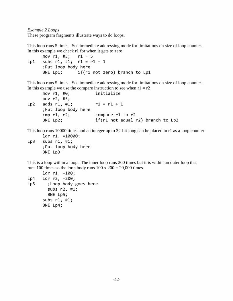
Example 2 Loops These program fragments illustrate ways to do loops. This loop runs 5 times. See immediate addressing mode for limitations on size of loop counter. In this example we check r1 for when it gets to zero. mov r1, #5; r1 = 5 Lp1 subs r1, #1; r1 = r1 – 1 ;Put loop body here BNE Lp1; if(r1 not zero) branch to Lp1 This loop runs 5 times. See immediate addressing mode for limitations on size of loop counter. In this example we use the compare instruction to see when r1 = r2 mov r1, #0; initialize mov r2, #5; Lp2 adds r1, #1; r1 = r1 + 1 ;Put loop body here cmp r1, r2; compare r1 to r2 BNE Lp2; if(r1 not equal r2) branch to Lp2 This loop runs 10000 times and an integer up to 32-bit long can be placed in r1 as a loop counter. ldr r1, =10000; Lp3 subs r1, #1; ;Put loop body here BNE Lp3 This is a loop within a loop. The inner loop runs 200 times but it is within an outer loop that runs 100 times so the loop body runs 100 x 200 = 20,000 times. ldr r1, =100; Lp4 ldr r2, =200; Lp5 ;Loop body goes here subs r2, #1; BNE Lp5; subs r1, #1; BNE Lp4;

-43-
Example 3 Logic This example uses assembly language to perform some logical operations. In the figure below
we can write CDABz +=
AND r0, r1, r2; r0 = r1 & r2 AND r3, r3, r4; r3 = r3 & r4 MVN r3, r3; r3 = (not)r3 ORR r0, r0, r3; r0 = A&B + (not)(C&D) MVN r0, r0; r0 = not r0 The MVN instruction is the mov not instruction. It moves the logical inverse of one register into another.
-44-
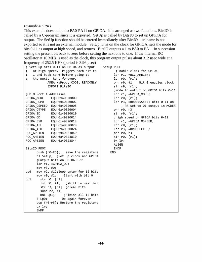
Example 4 GPIO This example does output to PA0-PA11 on GPIOA. It is arranged as two functions. BitsIO is called by a C-program since it is exported. SetUp is called by BitsIO to set up GPIOA for output. The SetUp function should be entered immediately after BitsIO – its name is not exported so it is not an external module. SetUp turns on the clock for GPIOA, sets the mode for bits 0-11 as output at high speed, and returns. BitsIO outputs a 1 to PA0 to PA11 in succession setting the present bit back to zero before setting the next one to one. If the internal RC oscillator at 16 MHz is used as the clock, this program output pulses about 312 nsec wide at a frequency of 252.5 KHz (period is 3.96 µsec) ; Sets up bits 0-11 on GPIOA as output ; at high speed. Triggers each bit to ; 1 and back to 0 before going to ; the next. Runs forever. AREA MyProg, CODE, READONLY EXPORT BitsIO ;GPIO Port A Addresses GPIOA_MODE EQU 0x40020000 GPIOA_PUPD EQU 0x4002000C GPIOA_OSPEED EQU 0x40020008 GPIOA_OTYPE EQU 0x40020004 GPIOA_ID EQU 0x40020010 GPIOA_OD EQU 0x40020014 GPIOA_BSR EQU 0x40020018 GPIOA_AFL EQU 0x40020020 GPIOA_AFH EQU 0x40020024 RCC_APB1EN EQU 0x40023840 RCC_AHB1EN EQU 0x40023830 RCC_APB2EN EQU 0x40023844 BitsIO PROC push {r0-R5}; save the registers bl SetUp; ;Set up clock and GPIOA ;Output bits on GPIOA 0-11 ldr r1, =GPIOA_OD; mov r3, #0; Lp0 mov r2, #12;loop cnter for 12 bits mov r0, #1; ;Start with bit 0 Lp1 str r0, [r1]; lsl r0, #1; ;shift to next bit str r3, [r1] ;clear bits subs r2, #1; BNE Lp1; ;Finish all 12 bits B Lp0; ;Do again forever pop {r0-r5}; Restore the registers bx lr; ENDP
SetUp PROC ;Enable clock for GPIOA ldr r1, =RCC_AHB1EN; ldr r0, [r1]; orr r0, #1; Bit 0 enables clock str r0, [r1]; ;Mode to output on GPIOA bits 0-11 ldr r1, =GPIOA_MODE; ldr r0, [r1]; ldr r3, =0x00555555; Bits 0-11 on ; PA set to 01 output in MODER orr r0, r3; str r0, [r1]; ;high speed on GPIOA bits 0-11 ldr r1, =GPIOA_OSPEED; ldr r0, [r1]; ldr r3, =0x00FFFFFF; orr r0, r3 str r0, [r1]; bx lr; ALIGN ENDP END

-45-
Example 5 D to A conversion This example illustrates the use of the two D to A converters (DACs). There is a main program in C which calls the two assembly language functions. One of these functions initializes one of two digital to analog converters and the appropriate analog output port. The other function accepts data and sends it to one of the two DACs. The code below is the main C-code. It calls DtoASetUp(0) one time for each DAC. If the argument is not zero it does a setup on DAC 1. DAC 0 outputs to PA4 and DAC 1 outputs to PA5. The setup program takes care of making these ports analog. For the DtoA function, the argument specifies the DAC number and the value to be sent to the DAC. The DACs are all 12-bit converters but the program does not check this data for validity. This program outputs a ramp function. #include "stm32f446.h" extern void DtoASetUp(int); extern void DtoA(int DtoANum, int value); int main() {int i, j; DtoASetUp(0); //Set up DAC Channel 0 for PA4 //DtoASetUp(1); //Set up DAC channel 1 for PA5 while(1) {for(i=0;i<4096;i++) {DtoA(0, i); //Or use DtoA(1, i) for DAC 1 for(j=0;j<200;j++); //Empty software delay } } } The assembly language programs make use of the following symbols defined with the EQU (Equate) directive. These addresses can be obtained from the "stm32f446.h" file or from the Reference manual (1). GPIOA_MODE EQU 0x40020000 GPIOA_PUPD EQU 0x4002000C GPIOA_OSPEED EQU 0x40020008 GPIOA_OTYPE EQU 0x40020004 GPIOA_ID EQU 0x40020010 GPIOA_OD EQU 0x40020014 GPIOA_BSR EQU 0x40020018 GPIOA_AFL EQU 0x40020020 GPIOA_AFH EQU 0x40020024 RCC_APB1EN EQU 0x40023840 RCC_AHB1EN EQU 0x40023830 RCC_APB2EN EQU 0x40023844 DAC_CONT EQU 0x40007400 DAC_SWTRIG EQU 0x40007404 DAC_DHR12Ch0 EQU 0x40007408 DAC_DHR12Ch1 EQU 0x40007414 DAC_DORCh1 EQU 0x4000742C
-46-
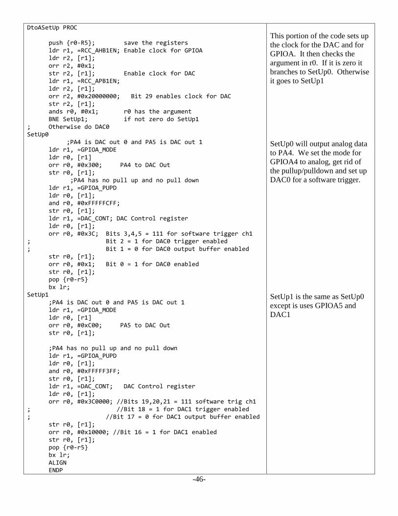
DtoASetUp PROC push {r0-R5}; save the registers ldr r1, =RCC_AHB1EN; Enable clock for GPIOA ldr r2, [r1]; orr r2, #0x1; str r2, [r1]; Enable clock for DAC ldr r1, =RCC_APB1EN; ldr r2, [r1]; orr r2, #0x20000000; Bit 29 enables clock for DAC str r2, [r1]; ands r0, #0x1; r0 has the argument BNE SetUp1; if not zero do SetUp1 ; Otherwise do DAC0 SetUp0 ;PA4 is DAC out 0 and PA5 is DAC out 1 ldr r1, =GPIOA_MODE ldr r0, [r1] orr r0, #0x300; PA4 to DAC Out str r0, [r1]; ;PA4 has no pull up and no pull down ldr r1, =GPIOA_PUPD ldr r0, [r1]; and r0, #0xFFFFFCFF; str r0, [r1]; ldr r1, =DAC_CONT; DAC Control register ldr r0, [r1]; orr r0, #0x3C; Bits 3,4,5 = 111 for software trigger ch1 ; Bit 2 = 1 for DAC0 trigger enabled ; Bit 1 = 0 for DAC0 output buffer enabled str r0, [r1]; orr r0, #0x1; Bit 0 = 1 for DAC0 enabled str r0, [r1]; pop {r0-r5} bx lr; SetUp1 ;PA4 is DAC out 0 and PA5 is DAC out 1 ldr r1, =GPIOA_MODE ldr r0, [r1] orr r0, #0xC00; PA5 to DAC Out str r0, [r1]; ;PA4 has no pull up and no pull down ldr r1, =GPIOA_PUPD ldr r0, [r1]; and r0, #0xFFFFF3FF; str r0, [r1]; ldr r1, =DAC_CONT; DAC Control register ldr r0, [r1]; orr r0, #0x3C0000; //Bits 19,20,21 = 111 software trig ch1 ; //Bit 18 = 1 for DAC1 trigger enabled ; //Bit 17 = 0 for DAC1 output buffer enabled str r0, [r1]; orr r0, #0x10000; //Bit 16 = 1 for DAC1 enabled str r0, [r1]; pop {r0-r5} bx lr; ALIGN ENDP
This portion of the code sets up the clock for the DAC and for GPIOA. It then checks the argument in r0. If it is zero it branches to SetUp0. Otherwise it goes to SetUp1 SetUp0 will output analog data to PA4. We set the mode for GPIOA4 to analog, get rid of the pullup/pulldown and set up DAC0 for a software trigger. SetUp1 is the same as SetUp0 except is uses GPIOA5 and DAC1

-47-
;*******This is the DtoA function that outputs the data to ; DAC0 or DAC1. In C-code use DtoA(DAC#, value) DtoA PROC push {r0-r5} cmp r0, #0 BNE DtoACh1; Check if DAC0 or DAC1 ldr r2, =DAC_DHR12Ch0 str r1, [r2]; Store data in DAC0 ldr r2, =DAC_SWTRIG ldr r3, [r2] orr r3, #0x1; Do software trigger str r3, [r2] pop {r0-r5} bx lr DtoACh1 ldr r2, =DAC_DHR12Ch1; DAC1 str r1, [r2]; ldr r2, =DAC_SWTRIG ldr r3, [r2] orr r3, #0x2 str r3, [r2] pop {r0-r5} bx lr ALIGN ENDP END
This is the D to A function which outputs the data to the DAC. If the first argument is 0 it outputs to DAC0. Otherwise, it outputs to DAC1.

-48-
C-Code Examples Example 1 GPIO This example sets up PA7 and PA9 for output and PB2 for input. It runs forever and each time through the loop it toggles PA7, does an input from PB2 and outputs that bit to PA9. /*GPIOInOut.c May 24, 2016 This program toggle pin PA7. It also inputs from pin PB2 and outputs to PA9 as fast as possible */ #include "stm32f446.h" int main() {int i, tmp; //Clock bits RCC_AHB1ENR |= 1; //Bit 0 is GPIOA clock enable bit RCC_AHB1ENR |= 2; //Bit 1 is GPIOB clock enable bit //I/O bits PA7 GPIOA_MODER |= 0x4000; //Bits 15-14 = 01 for digital output on PA7 //OTYPER register resets to 0 so it is push/pull by default GPIOA_OSPEEDER |= 0xC000; //Bits 15-14 = 11 for high speed on PA7 //PUPDR defaults to no pull up no pull down //I/O bits PA9 GPIOA_MODER |= 0x40000; //Bits 18-19 = 01 for digital output on PA9 //OTYPER register resets to 0 so it is push/pull by default GPIOA_OSPEEDER |= 0xC0000; //Bits 18-19 = 11 for high speed on PA9 //PUPDR defaults to no pull up no pull down //I/O bits PB2 GPIOB_OSPEEDER |= 0xC; //PB2 to high speed //All bits are input by default. //Main program loop tmp = 0; while(1) {if(tmp == 0) GPIOA_ODR &= ~(1 << 7); //Only PA7 is set up for output so other bits else GPIOA_ODR |= (1 << 7); tmp = ~tmp; // have no effect. //Input bit PB2 and shift it 7 places to output to PA9 if((GPIOB_IDR & 0x4) == 0) GPIOA_ODR |= (1 << 9); else GPIOA_ODR &= ~(1 << 9); //for(i=0;i<10000;i++); //Put this in to slow down toggle } }

-49-
Example 2 A to D and D to A Conversion This example uses the ADC and DAC. An analog signal is read from PA5 on ADC0 and sent to PA4 on DAC0. You can input a signal in the range of 0 to 3 volts on PA5 and see the sampled signal on PA4. The software delay slows the sampling time. //AtoDtoATest.c /* This program inputs and analog signal from PA5 on the ARM M4 Nucleo board and outputs the same analog signal with no scaling to PA4. */ #include "stm32f446.h" int main() {int i; RCC_AHB1ENR |= 1; //Bit 0 is GPIOA clock enable bit RCC_APB1ENR |= (1 << 29); //Bit 29 is DAC clock enable bit RCC_APB2ENR |= 0x100; //Bit 8 is ADC 1 clock enable bit GPIOA_MODER |= 0xF00; //PA4-PA5 are analog GPIOA_PUPDR &= 0xFFFFF0FF; //Pins PA4 PA5 are no pull up and no pull down DAC_CR |= 0x3C; //Bits 3, 4, 5 = 111 for software trigger ch1 //Bit 2 = 1 for Ch 1 trigger enabled //Bit 1 = 1 for Ch 1 output buffer enabled DAC_CR |= 1; //Bit 0 = 0 for Ch 1 enabled ADC1_CR2 |= 1; //Bit 0 turn ADC on ADC1_CR2 |= 0x400; //Bit 10 allows EOC to be set after conversion ADC_CCR |= 0x30000; //Bits 16 and 17 = 11 so clock divided by 8 ADC1_SQR3 |= 0x5; //Bits 4:0 are channel number for first conversion // Channel is set to 5 which corresponds to PA5 while(1) {ADC1_CR2 |= 0x40000000; // Bit 30 does software start of A/D conversion while((ADC1_SR & 0x2) == 0); //Bit 1 is End of Conversion DAC_DHR12R1 = ADC1_DR & 0xFFF; DAC_SWTRIGR |= 0x1; //Start the D/A conversion for(i=0;i<200;i++); } }
-50-
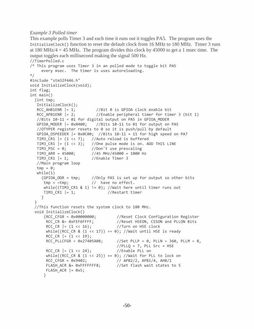
Example 3 Polled timer This example polls Timer 3 and each time it runs out it toggles PA5. The program uses the InitializeClock() function to reset the default clock from 16 MHz to 180 MHz. Timer 3 runs at 180 MHz/4 = 45 MHz. The program divides this clock by 45000 to get a 1 msec time. The output toggles each millisecond making the signal 500 Hz. //TimerPolled.c /* This program uses Timer 3 in an polled mode to toggle bit PA5 every msec. The timer is uses autoreloading. */ #include "stm32f446.h" void InitializeClock(void); int flag; int main() {int tmp; InitializeClock(); RCC_AHB1ENR |= 1; //Bit 0 is GPIOA clock enable bit RCC_APB1ENR |= 2; //Enable peripheral timer for timer 3 (bit 1) //Bits 10-11 = 01 for digital output on PA5 in GPIOA_MODER GPIOA_MODER |= 0x0400; //Bits 10-11 to 01 for output on PA5 //OTYPER register resets to 0 so it is push/pull by default GPIOA_OSPEEDER |= 0x0C00; //Bits 10-11 = 11 for high speed on PA7 TIM3_CR1 |= (1 << 7); //Auto reload is buffered TIM3_CR1 |= (1 << 3); //One pulse mode is on. ADD THIS LINE TIM3_PSC = 0; //Don't use prescaling TIM3_ARR = 45000; //45 MHz/45000 = 1000 Hz TIM3_CR1 |= 1; //Enable Timer 3 //Main program loop tmp = 0; while(1) {GPIOA_ODR = tmp; //Only PA5 is set up for output so other bits tmp = ~tmp; // have no effect. while((TIM3_CR1 & 1) != 0); //Wait here until timer runs out TIM3_CR1 |= 1; //Restart timer } } //This function resets the system clock to 180 MHz. void InitializeClock() {RCC_CFGR = 0x00000000; //Reset Clock Configuration Register RCC_CR &= 0xFEF6FFFF; //Reset HSEON, CSSON and PLLON Bits RCC_CR |= (1 << 16); //Turn on HSE clock while((RCC_CR & (1 << 17)) == 0); //Wait until HSE is ready RCC_CR |= (1 << 19); RCC_PLLCFGR = 0x27405A08; //Set PLLP = 0, PLLN = 360, PLLM = 8, //PLLQ = 7, PLL Src = HSE RCC_CR |= (1 << 24); //Enable PLL on while((RCC_CR & (1 << 25)) == 0); //Wait for PLL to lock on RCC_CFGR = 0x9402; // APB2/2, APB1/4, AHB/1 FLASH_ACR &= 0xFFFFFFF8; //Set flash wait states to 5 FLASH_ACR |= 0x5; }

-51-
Example 4 Timer interrupt This example is the same as Example 3 except that it uses an interrupt which is triggered by the expired timer and it uses the default clock rate of 16 MHz. The signal on PA5 is about 500 Hz. //Timer2Int.c /* This program uses Timer 2 in an interrupt mode to toggle bit PA5 about every 1 msec. The timer uses autoreloading. The default clock at 16 MHz is used. */ #include "stm32f446.h" int flag; int main() {int tmp; //Clock bits RCC_AHB1ENR |= 1; //Bit 0 is GPIOA clock enable bit RCC_APB1ENR |= 1; //Enable peripheral timer for timer 2 (bit 0) //Interrupt bits NVICISER0 |= (1 << 28); //Bit 28 in ISER0 corresponds to int 28 (TIM 2) TIM2_DIER |= 1; //Enable Timer 2 update interrupt enable TIM2_DIER |= (1 << 6); //Enable Timer 2 trigger interrupt enable //I/O bits //Bits 10-11 = 01 for digital output on PA5 in GPIOA_MODER GPIOA_MODER |= 0x0400; //Bits 10-11 to 01 for output on PA5 //OTYPER register resets to 0 so it is push/pull by default GPIOA_OSPEEDER |= 0x0C00; //Bits 10-11 = 11 for high speed on PA7 //PUPDR defaults to no pull up no pull down //Timer 2 bits TIM2_CR1 |= (1 << 7); //Auto reload is buffered TIM2_PSC = 0; //Don't use prescaling TIM2_ARR = 16000; //16MHz/16000 = 1000 Hz TIM2_CR1 |= 1; //Enable Timer 2 TIM2_EGR |= 1; //Main program loop tmp = 0; while(1) {GPIOA_ODR = tmp; //Only PA5 is set up for output so other bits tmp = ~tmp; // have no effect. flag = 1; while(flag == 1); TIM2_CR1 |= 1; //Restart timer } } void TIM2_IRQHandler() {flag = 0; TIM2_SR &= 0xFFFE; //Turn off interrupt }

-52-
Example 5 Real Time Clock This program sets up a real time clock with global variables that keep track of milliseconds, seconds, and minutes. It uses Timer 3 with an interrupt similar to that used in Example 4. //RTC.c /* This program uses Timer 3 in an interrupt mode to update a real time clock variable every millisecond. */ #include "stm32f446.h" int seconds; int tenthsCounter; int milliSeconds; int minutes; int main() {//Clock bits RCC_APB1ENR |= 2; //Enable peripheral timer for timer 3 (bit 1) //Interrupt bits NVICISER0 |= (1 << 29); //Bit 29 in ISER0 corresponds to int 29 (TIM 3) TIM3_DIER |= 1; //Enable Timer 3 update interrupt enable TIM3_DIER |= (1 << 6); //Enable Timer 3 trigger interrupt enable //Timer 3 bits TIM3_CR1 |= (1 << 7); //Auto reload is buffered TIM3_PSC = 0; //Don't use prescaling TIM3_ARR = 16000; //16 MHz/16000 = 1000 Hz TIM3_CR1 |= 1; //Enable Timer 3 //Main program loop minutes = 0; milliSeconds = 0; tenthsCounter = 0; seconds = 0; while(1); } void TIM3_IRQHandler() {milliSeconds++; if(milliSeconds > 99) //.1 sec = 100 msec {milliSeconds = 0; tenthsCounter++; if(tenthsCounter > 9) //For each 10 update seconds {tenthsCounter = 0; seconds++; if(seconds > 59) //For each 60 seconds update minutes {seconds = 0; minutes++; //minutes can overflow } } } TIM3_SR &= 0xFFFE; //Turn off interrupt TIM3_CR1 |= 1; //Restart timer }
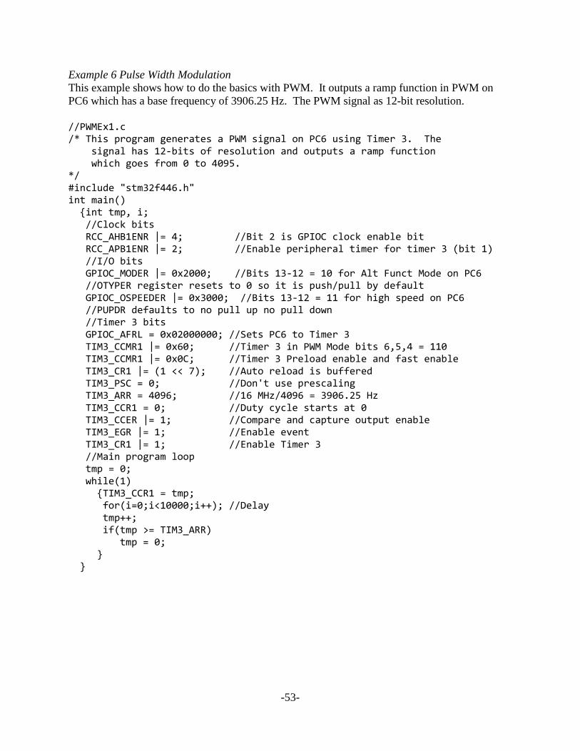
-53-
Example 6 Pulse Width Modulation This example shows how to do the basics with PWM. It outputs a ramp function in PWM on PC6 which has a base frequency of 3906.25 Hz. The PWM signal as 12-bit resolution. //PWMEx1.c /* This program generates a PWM signal on PC6 using Timer 3. The signal has 12-bits of resolution and outputs a ramp function which goes from 0 to 4095. */ #include "stm32f446.h" int main() {int tmp, i; //Clock bits RCC_AHB1ENR |= 4; //Bit 2 is GPIOC clock enable bit RCC_APB1ENR |= 2; //Enable peripheral timer for timer 3 (bit 1) //I/O bits GPIOC_MODER |= 0x2000; //Bits 13-12 = 10 for Alt Funct Mode on PC6 //OTYPER register resets to 0 so it is push/pull by default GPIOC_OSPEEDER |= 0x3000; //Bits 13-12 = 11 for high speed on PC6 //PUPDR defaults to no pull up no pull down //Timer 3 bits GPIOC_AFRL = 0x02000000; //Sets PC6 to Timer 3 TIM3_CCMR1 |= 0x60; //Timer 3 in PWM Mode bits 6,5,4 = 110 TIM3_CCMR1 |= 0x0C; //Timer 3 Preload enable and fast enable TIM3_CR1 |= (1 << 7); //Auto reload is buffered TIM3_PSC = 0; //Don't use prescaling TIM3_ARR = 4096; //16 MHz/4096 = 3906.25 Hz TIM3_CCR1 = 0; //Duty cycle starts at 0 TIM3_CCER |= 1; //Compare and capture output enable TIM3_EGR |= 1; //Enable event TIM3_CR1 |= 1; //Enable Timer 3 //Main program loop tmp = 0; while(1) {TIM3_CCR1 = tmp; for(i=0;i<10000;i++); //Delay tmp++; if(tmp >= TIM3_ARR) tmp = 0; } }
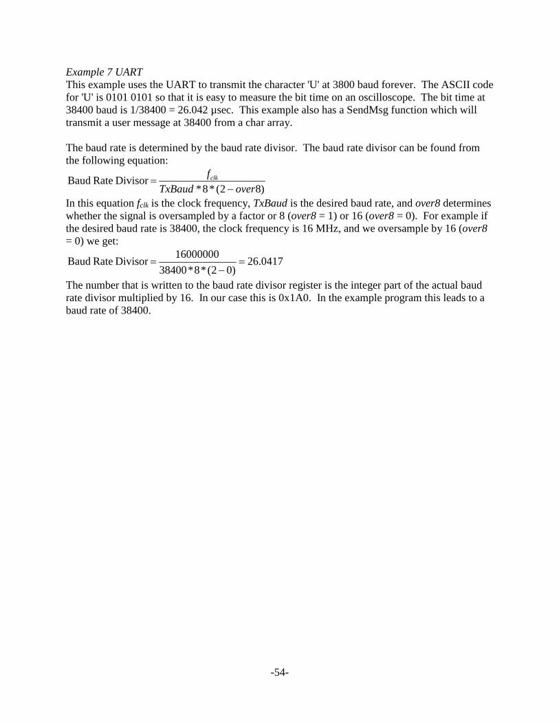
-54-
Example 7 UART This example uses the UART to transmit the character 'U' at 3800 baud forever. The ASCII code for 'U' is 0101 0101 so that it is easy to measure the bit time on an oscilloscope. The bit time at 38400 baud is 1/38400 = 26.042 µsec. This example also has a SendMsg function which will transmit a user message at 38400 from a char array. The baud rate is determined by the baud rate divisor. The baud rate divisor can be found from the following equation:
)82(*8* Divisor Rate Baud
overTxBaudfclk
−=
In this equation fclk is the clock frequency, TxBaud is the desired baud rate, and over8 determines whether the signal is oversampled by a factor or 8 (over8 = 1) or 16 (over8 = 0). For example if the desired baud rate is 38400, the clock frequency is 16 MHz, and we oversample by 16 (over8 = 0) we get:
0417.26)02(*8*38400
16000000 Divisor Rate Baud =−
=
The number that is written to the baud rate divisor register is the integer part of the actual baud rate divisor multiplied by 16. In our case this is 0x1A0. In the example program this leads to a baud rate of 38400.

-55-
//UARTEx1.c /* Transmits the character 'U' at 38400 baud on USART6 PC6 forever. */ #include "stm32f446.h" void ConfigureUART(unsigned int baudDivisor); void UARTPutChar(char ch); void SendMsg(const char msg[]); int main() { //Clock bits RCC_AHB1ENR |= 4; //Bit 3 is GPIOC clock enable bit //RCC_APB1ENR |= (1 << 4); //Enable peripheral timer for timer 6 RCC_APB2ENR |= (1 << 5); //Enable USART6 clock //UART PIN Bits GPIOC_AFRL = 0x88000000; //Alternate Func PC 6-7 to USART6 GPIOC_MODER |= 0x0A000; //Bits 15-12 = 1010 for Alt Func on PC6, PC7 //OTYPER register resets to 0 so it is push/pull by default GPIOC_OSPEEDER |= 0x3000; //Bits 7-6 = 11 for high speed on PC6 //PUPDR defaults to no pull up no pull down //USART1 bits GPIOA_MODER |= 0x40000; //Bits 18-19 are 01 for digital output on PA9 GPIOA_OSPEEDER |= 0xC0000; //Bits 18-19 are 11 for high speed on PA9 //PA10 is input by default ConfigureUART(0x1A0); while(1) UARTPutChar('U'); } // void ConfigureUART(unsigned int baudDivisor) {USART6_CR1 = 0; //Disable during set up. Wd len = 8, Parity = off USART6_BRR = baudDivisor; //Set up baud rate USART6_CR2 = 0; //1 stop bit USART6_CR1 = 0x200C; USART6_CR3 = 0; //Disable interrupts and DMA } // void UARTPutChar(char ch) {//Wait for empty flag while((USART6_SR & 0x80) == 0); USART6_DR = ch; } // void SendMsg(const char msg[]) {int i = 0; while(msg[i] != 0) {UARTPutChar(msg[i]); i++; } }
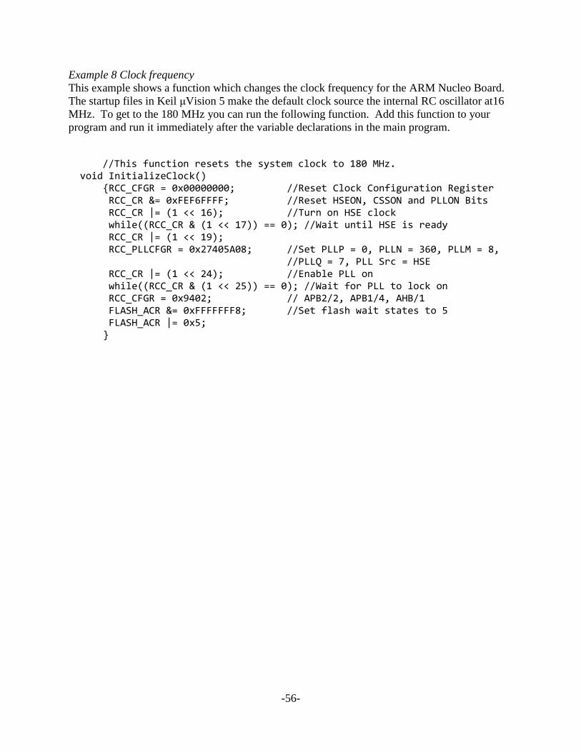
-56-
Example 8 Clock frequency This example shows a function which changes the clock frequency for the ARM Nucleo Board. The startup files in Keil μVision 5 make the default clock source the internal RC oscillator at16 MHz. To get to the 180 MHz you can run the following function. Add this function to your program and run it immediately after the variable declarations in the main program. //This function resets the system clock to 180 MHz. void InitializeClock() {RCC_CFGR = 0x00000000; //Reset Clock Configuration Register RCC_CR &= 0xFEF6FFFF; //Reset HSEON, CSSON and PLLON Bits RCC_CR |= (1 << 16); //Turn on HSE clock while((RCC_CR & (1 << 17)) == 0); //Wait until HSE is ready RCC_CR |= (1 << 19); RCC_PLLCFGR = 0x27405A08; //Set PLLP = 0, PLLN = 360, PLLM = 8, //PLLQ = 7, PLL Src = HSE RCC_CR |= (1 << 24); //Enable PLL on while((RCC_CR & (1 << 25)) == 0); //Wait for PLL to lock on RCC_CFGR = 0x9402; // APB2/2, APB1/4, AHB/1 FLASH_ACR &= 0xFFFFFFF8; //Set flash wait states to 5 FLASH_ACR |= 0x5; }
-57-
References
1. STM32F446xx Reference Manual RM0390. http://www.st.com/content/ccc/resource/technical/document/reference_manual/4d/ed/bc/89/b5/70/40/dc/DM00135183.pdf/files/DM00135183.pdf/jcr:content/translations/en.DM00135183.pdf 2. STM32F4 Programming Manual PM0214 http://www.st.com/content/ccc/resource/technical/document/programming_manual/6c/3a/cb/e7/e4/ea/44/9b/DM00046982.pdf/files/DM00046982.pdf/jcr:content/translations/en.DM00046982.pdf 3. Nucleo Board User's Manual UM1724 http://www.st.com/content/ccc/resource/technical/document/user_manual/98/2e/fa/4b/e0/82/43/b7/DM00105823.pdf/files/DM00105823.pdf/jcr:content/translations/en.DM00105823.pdf 4. Stallings, William, Computer Organization and Architecture, Prentice-Hall, 2016 5. STM32F446RE Data sheet http://www.st.com/content/ccc/resource/technical/document/datasheet/65/cb/75/50/53/d6/48/24/DM00141306.pdf/files/DM00141306.pdf/jcr:content/translations/en.DM00141306.pdf 6. Architectural Features of the Cortex M4 https://eda360insider.wordpress.com/2011/09/22/ingenious-architectural-features-allow-st-micro-to-extract-maximum-performance-from-new-microcontroller-family-based-on-arm-cortex-m4-cost-less-than-6-bucks-in-1000s/ 7. ARM Cortex M4 Technical Reference Manual http://infocenter.arm.com/help/topic/com.arm.doc.100166_0001_00_en/arm_cortexm4_processor_trm_100166_0001_00_en.pdf 8. Yiu, Joseph, The Definitive Guide to ARM Cortex M3 and Cortex M4 Processors, Third Edition, Elsevier, 2014. 9. ARM Compiler toolchain Assembler Reference, ARM DUI 0489C Copyright © 2010-2011 ARM. ID080411 http://infocenter.arm.com/help/topic/com.arm.doc.dui0489c/DUI0489C_arm_assembler_reference.pdf