stochastic-based computing with emerging spin-based device
TRANSCRIPT

University of Central Florida University of Central Florida
STARS STARS
Electronic Theses and Dissertations, 2004-2019
2016
Stochastic-Based Computing with Emerging Spin-Based Device Stochastic-Based Computing with Emerging Spin-Based Device
Technologies Technologies
Yu Bai University of Central Florida
Part of the Electrical and Computer Engineering Commons
Find similar works at: https://stars.library.ucf.edu/etd
University of Central Florida Libraries http://library.ucf.edu
This Doctoral Dissertation (Open Access) is brought to you for free and open access by STARS. It has been accepted
for inclusion in Electronic Theses and Dissertations, 2004-2019 by an authorized administrator of STARS. For more
information, please contact [email protected].
STARS Citation STARS Citation Bai, Yu, "Stochastic-Based Computing with Emerging Spin-Based Device Technologies" (2016). Electronic Theses and Dissertations, 2004-2019. 5424. https://stars.library.ucf.edu/etd/5424

STOCHASTIC-BASED COMPUTING WITH EMERGING SPIN-BASED DEVICETECHNOLOGIES
by
YU BAIM.S. University of Texas-Pan America, 2011
B.S. National Aviation University, 2008
A dissertation submitted in partial fulfilment of the requirementsfor the degree of Doctor of Philosophy
in the Department of Electrical Engineering and Computer Sciencein the College of Engineering and Computer Science
at the University of Central FloridaOrlando, Florida
Summer Term2016
Major Professor: Mingjie Lin

c© 2016Yu Bai
ii

ABSTRACT
In this dissertation, analog and emerging device physics is explored to provide a technology plat-
form to design new bio-inspired system and novel architecture. With CMOS approaching the
nano-scaling, their physics limits in feature size. Therefore, their physical device characteristics
will pose severe challenges to constructing robust digital circuitry. Unlike transistor defects due to
fabrication imperfection, quantum-related switching uncertainties will seriously increase their sus-
ceptibility to noise, thus rendering the traditional thinking and logic design techniques inadequate.
Therefore, the trend of current research objectives is to create a non-Boolean high-level compu-
tational model and map it directly to the unique operational properties of new, power efficient,
nanoscale devices.
The focus of this research is based on two-fold: 1) Investigation of the physical hysteresis switching
behaviors of domain wall device. We analyze phenomenon of domain wall device and identify hys-
teresis behavior with current range. We proposed the Domain-Wall-Motion-based (DWM) NCL
circuit that achieves approximately 30x and 8x improvements in energy efficiency and chip layout
area, respectively, over its equivalent CMOS design, while maintaining similar delay performance
for a one bit full adder. 2) Investigation of the physical stochastic switching behaviors of Mag-
netic Tunnel Junction (MTJ) device. With analyzing of stochastic switching behaviors of MTJ, we
proposed an innovative stochastic-based architecture for implementing artificial neural network
(S-ANN) with both magnetic tunneling junction (MTJ) and domain wall motion (DWM) devices,
which enables efficient computing at an ultra-low voltage. For a well-known pattern recognition
task, our mixed-model HSPICE simulation results have shown that a 34-neuron S-ANN imple-
mentation, when compared with its deterministic-based ANN counterparts implemented with dig-
ital and analog CMOS circuits, achieves more than 1.5 ∼ 2 orders of magnitude lower energy
consumption and 2 ∼ 2.5 orders of magnitude less hidden layer chip area.
iii

ACKNOWLEDGMENTS
I would like to first sincerely thank my wife and parents for their endless love, support, and en-
couragement. Secondly, I would like to thank my Ph.D. research advisor, Professor Mingjie Lin,
for his patient guidance, encouragement, and support during my studies and research. I am truly
fortunate to have him as an advisor, and any of the research in this dissertation would not have
been possible without him.
I would also like to thank Prof. Ronald F. DeMara, Prof. Jun Wang, Prof. Yier Jin, and Prof.
Yajie Dong for serving on the advisory committee and providing me with valuable comments and
suggestions to improve my research.
iv
TABLE OF CONTENTS
LIST OF FIGURES . . . . . . . . . . . . . . . . . . . . . . . . . . . . . . . . . . . . . . ix
LIST OF TABLES . . . . . . . . . . . . . . . . . . . . . . . . . . . . . . . . . . . . . . .xviii
CHAPTER 1: INTRODUCTION . . . . . . . . . . . . . . . . . . . . . . . . . . . . . . 1
CHAPTER 2: BASIC PRINCIPLES OF SPINTRONICS DEVICE . . . . . . . . . . . . . 5
Introduction . . . . . . . . . . . . . . . . . . . . . . . . . . . . . . . . . . . . . . . . . 5
Two Terminal Magnetic Tunnel Junction . . . . . . . . . . . . . . . . . . . . . . . . . . 5
Domain Wall Device . . . . . . . . . . . . . . . . . . . . . . . . . . . . . . . . . . . . 7
Ferromagnetic Spin Orbit Torque Device . . . . . . . . . . . . . . . . . . . . . . . . . . 10
CHAPTER 3: ULTRA-ROBUST NULL CONVENTION LOGIC CIRCUIT WITH EMERG-
ING DOMAIN WALL DEVICES . . . . . . . . . . . . . . . . . . . . . . . 16
Introduction . . . . . . . . . . . . . . . . . . . . . . . . . . . . . . . . . . . . . . . . . 16
NCL Concept and Circuit Design . . . . . . . . . . . . . . . . . . . . . . . . . . . . . . 18
Why All Spin Torque Null Convention Logic . . . . . . . . . . . . . . . . . . . . . . . 20
Proposed All Spin Torque Null Convention Logic . . . . . . . . . . . . . . . . . . . . . 22
v

Transformation From Boolean NCL to Spin Torque NCL . . . . . . . . . . . . . . . . . 24
Proposed Asynchronous Circuit Design Through Magnetic Domain Wall NCL Gate . . . 32
The Performance Analysis and Discussion . . . . . . . . . . . . . . . . . . . . . . . . . 37
Large Scale Application of Proposed NCL Architecture . . . . . . . . . . . . . . . . . . 40
Memristor error analysis . . . . . . . . . . . . . . . . . . . . . . . . . . . . . . . . . . 43
Domain wall error analysis . . . . . . . . . . . . . . . . . . . . . . . . . . . . . . . . . 45
Conclusion . . . . . . . . . . . . . . . . . . . . . . . . . . . . . . . . . . . . . . . . . 45
CHAPTER 4: DESIGN OF STOCHASTIC ARTIFICIAL NEURAL NETWORK THROUGH
EMERGING DEVICES . . . . . . . . . . . . . . . . . . . . . . . . . . . . 47
Introduction . . . . . . . . . . . . . . . . . . . . . . . . . . . . . . . . . . . . . . . . . 47
Prior Work on ANN Hardware Implementation . . . . . . . . . . . . . . . . . . . . . . 50
Why Stochastic-based ANN? . . . . . . . . . . . . . . . . . . . . . . . . . . . . . . . . 52
Stochastic-Based Artificial Neural Network . . . . . . . . . . . . . . . . . . . . . . . . 54
Stochastic Switching of MTJ and DWM Devices . . . . . . . . . . . . . . . . . . . . . 56
Stochastic-Based Synapse with STT Device . . . . . . . . . . . . . . . . . . . . . . . . 59
Stochastic-based Soft-limiting Neuron . . . . . . . . . . . . . . . . . . . . . . . . . . . 66
Hardware Implementation of S-ANN . . . . . . . . . . . . . . . . . . . . . . . . . . . . 69
vi

S-ANN for Pattern Recognition:
Results and Performance . . . . . . . . . . . . . . . . . . . . . . . . . . . . . . . 71
Analytical Error Study . . . . . . . . . . . . . . . . . . . . . . . . . . . . . . . . . . . 78
Conclusion . . . . . . . . . . . . . . . . . . . . . . . . . . . . . . . . . . . . . . . . . 80
CHAPTER 5: SPIN-TRANSFER-TORQUE-DRIVEN AND NEURON-BASED FPGA AR-
CHITECTURE WITH EMERGING DEVICES . . . . . . . . . . . . . . . 81
Introduction . . . . . . . . . . . . . . . . . . . . . . . . . . . . . . . . . . . . . . . . . 81
Architecture Overview of SN-FPGA . . . . . . . . . . . . . . . . . . . . . . . . . . . . 85
MIMO-LUT: Idea and Methodology . . . . . . . . . . . . . . . . . . . . . . . . . . . . 86
Algebraically Reinterpreting LUT . . . . . . . . . . . . . . . . . . . . . . . . . . . . . 88
MIMO-LUT with Artificial Neural Network . . . . . . . . . . . . . . . . . . . . . . . . 90
MIMO-LUT: Circuit Implementation . . . . . . . . . . . . . . . . . . . . . . . . . . . . 92
Spin-Transfer-Torque-based Artificial Neural Network . . . . . . . . . . . . . . . . . . 92
All Spin Neural Synapse . . . . . . . . . . . . . . . . . . . . . . . . . . . . . . . . . . 94
All Spin Neuron . . . . . . . . . . . . . . . . . . . . . . . . . . . . . . . . . . . . . . . 98
Final Piece: Flip-Flops . . . . . . . . . . . . . . . . . . . . . . . . . . . . . . . . . . . 101
4:2 Encoder Implemented with Spin-Based LUT . . . . . . . . . . . . . . . . . . . . . . 103
Performance Analysis and Comparison . . . . . . . . . . . . . . . . . . . . . . . . . . . 105
vii

Conclusion . . . . . . . . . . . . . . . . . . . . . . . . . . . . . . . . . . . . . . . . . 112
CHAPTER 6: CONCLUSION . . . . . . . . . . . . . . . . . . . . . . . . . . . . . . . . 114
LIST OF REFERENCES . . . . . . . . . . . . . . . . . . . . . . . . . . . . . . . . . . . 116
viii

LIST OF FIGURES
Figure 1.1: (a). Exponential increase in power leakage of CMOS device. (b). Tempo-
ral degradation of performance of CMOS device [48]. . . . . . . . . . . . 1
Figure 1.2: (a). CMOS device switching energy. (b). Spintronics device switching
energy. . . . . . . . . . . . . . . . . . . . . . . . . . . . . . . . . . . . . 2
Figure 2.1: Simplified Magnetic Tunnel Junction (MTJ) structure . . . . . . . . . . . . 6
Figure 2.2: (a) Structure of an MTJ device[117]. (b) Our SPICE simulation results
of random signal generation. (c) Experimental and analytical results of
switching probability vs. the pulse duration at different voltages [106, 39,
83]. . . . . . . . . . . . . . . . . . . . . . . . . . . . . . . . . . . . . . . 7
Figure 2.3: Schematic illustration of domain wall motion device. (a) Simplistic con-
ceptual view. (b) More realistic Three-terminal DWM cell structure. (b)
Equivalent circuital view. . . . . . . . . . . . . . . . . . . . . . . . . . . . 8
Figure 2.4: (a) Simulation of domain wall moving by current injection in terminal T1,
the domain wall is moving to right by the spin polarized electrons. (b)
Compact model presents good agreement with micromagnetic simulation
for DW motion speed V as a function of current density jp [117]. (c). A
non-zero current inject to DW motion and obtains results in a hysteresis in
the DW switching characteristics [35, 64]. . . . . . . . . . . . . . . . . . . 9
ix

Figure 2.5: The physical phenomena of SHE assisted domain wall device. The domain
wall is moving in PMA nanowires according to flow of in-plane injec-
tion current through HM layer. The SOT coupling is generated and makes
stabilization of chiral Neel domain wall through DMI. According to this
model, a transverse spin current is generated by in-plane injection current.
The top and down view is shown in Fig. 2.5. . . . . . . . . . . . . . . . . 11
Figure 2.6: Schematic spin neuron device with spin torque layer. (a) Three-terminal
DWM cell structure. (b) DW speed with and without SHE assist. (c) DW
switch characteristics. The hysteresis characteristics depends on critical
current Ic of DW moving. . . . . . . . . . . . . . . . . . . . . . . . . . . 13
Figure 2.7: Mumax3 simulation of DW motion according to injected current of 25µA
flowing through the HM layer in 0.3ns. The given FM layer is 100nm in
length with ferromagnet thickness 0.6nm. . . . . . . . . . . . . . . . . . . 14
Figure 3.1: NCL overall scheme: input wavefronts are controlled by local handshak-
ing and completion detection signals. (a) Traditional NCL pipeline. (b)
Symbol and structure of threshold gate TH23. (c) Implementation of logic
function Z = X ⊕ Y . (d) Two-bit register and completion detector. . . . . 18
Figure 3.2: (a). Layout of single domain wall with 2 access transistor. (b). Layout of
two bit domain wall with 3 access transistor. . . . . . . . . . . . . . . . . 21
Figure 3.3: (a) TH23 static NCL gates. (b) TH23 DWL NCL gate. . . . . . . . . . . . 22
Figure 3.4: Simulation of proposed TH44 gate through domain wall logic device. . . . 26
x

Figure 3.5: (a) CMOS NCL THXOR gate (b) CMOS NCL THand0 gate (c) CMOS
NCL TH24comp gate (d) Spin-torque-transfer DW device based NCL THXOR
gate architecture (e) Spin-torque-transfer DW device based NCL THand0
gate architecture (f) Spin-torque-transfer DW device based NCL TH24comp
gate architecture (g) Simulation of Spin-torque-transfer DW device based
NCL THXOR gate architecture (h) Simulation of Spin-torque-transfer DW
device based NCL THand0 gate architecture (i) Simulation of Spin-torque-
transfer DW device based NCL TH24comp gate architecture . . . . . . . . 31
Figure 3.6: (a) Dual rail spin torque NCL architecture with reading scheme. (b) Sim-
ulation of NPN transistor with different supplied voltage Vcc. The input
current is generated from DW sensing current and amplified through NPN
transistor. . . . . . . . . . . . . . . . . . . . . . . . . . . . . . . . . . . . 32
Figure 3.7: (a). DWL duail rail NCL implementation, the two dual rail bits can be
implemented through two domain wall device which is separated by shared
terminals. (b). The equivalence analog circuit of proposed DWL duail rail
architecture in NULL case. (c). The equivalence analog circuit of proposed
DWL duail rail architecture in DATA 1 case . (d).The equivalence analog
circuit of proposed DWL duail rail architecture in DATA0 case. (e). The
DWL dual rail 4-phase communication protocol. (f). DWL asynchronous
QDI pipeline architecture, the input is controlled by local handshaking and
completion detection signal (ACK). . . . . . . . . . . . . . . . . . . . . . 36
Figure 3.8: (a). DWL duail rail NCL architecture of one bit full adder. (b). CMOS
duail rail NCL architecture of one bit full adder. . . . . . . . . . . . . . . . 36
Figure 3.9: Simulation of proposed DWL NCL full adder. . . . . . . . . . . . . . . . . 37
xi

Figure 3.10: (a). Delay measurement of different selected TH gate. (b). Energy mea-
surement of different selected TH gate. (c). Area measurement of different
selected TH gate. . . . . . . . . . . . . . . . . . . . . . . . . . . . . . . 38
Figure 3.11: (a). Delay measurement of NCL full adder with increasing bits. (b). En-
ergy measurement in log scale of NCL full adder with increasing bits.(c).
Area measurement in log scale of NCL full adder with increasing bits. . . 39
Figure 3.12: IEEE single precision floating point co-processor architecture [119]. . . . . 41
Figure 3.13: CAD flow of DWNCL simulation framework . . . . . . . . . . . . . . . . 41
Figure 3.14: (a). Memristor refresh architecture, the refresh signal is controlled by in-
puts of DW reset signal and acknowledge signal from next stage. (b). The
waveform of control signal in R/W control module. (c). The memristor
drift simulation of different input current with time increasing. (d). The
memristor drift simulation of different pulse duration current with input
current increasing. . . . . . . . . . . . . . . . . . . . . . . . . . . . . . . 43
Figure 4.1: Structure of an artificial neuron. It consists of three computation blocks.
The weighted sum of all inputs are passed to its output through a transfer
function. Four most common transfer functions are shown on right side of
Fig. 4.1. . . . . . . . . . . . . . . . . . . . . . . . . . . . . . . . . . . . . 48
Figure 4.2: Taxonomy of current ANN designs. Con: CMOS Technology; Em: Emerg-
ing Device Technology. . . . . . . . . . . . . . . . . . . . . . . . . . . . 50
xii

Figure 4.3: (a) MTJ device resistance histogram distribution of two statesRP andRAP
under σ/µ = 5%, 10%, and 25% of device resistance (b) Comparison of
weight variation on memristor based method and MTJ stochastic based
method . . . . . . . . . . . . . . . . . . . . . . . . . . . . . . . . . . . . 52
Figure 4.4: Architecture of proposed stochastic neuron . . . . . . . . . . . . . . . . . 55
Figure 4.5: (a) Spin-torque-transfer DW device structure (b) Micro-magnetic simu-
lation of free layer DW motion when injected current density is 1.5 ×
1013A/m2 . . . . . . . . . . . . . . . . . . . . . . . . . . . . . . . . . . 57
Figure 4.6: Circuit design of random bit stream generation. (a) Configuration mode.
(b) Operation mode. Devices in gray area are active for each mode. Red
curves depict signal directions. (c) HSPICE simulation of MTJ stochas-
tic switching in 3 different devices which are programmed with different
probability values. . . . . . . . . . . . . . . . . . . . . . . . . . . . . . . 59
Figure 4.7: (a) Simulation of NPN transistor with different supplied voltages Vcc, where
the input current is generated from a DW sensing current and amplified
through a NPN transistor (b) Simulation of a NPN transistor with different
parameters β . . . . . . . . . . . . . . . . . . . . . . . . . . . . . . . . . 61
Figure 4.8: (a) The equivalent DW position used for generating corresponding proba-
bility through MTJ device (b) The equivalent writing current used to inject
into DW device for generating corresponding probability through MTJ de-
vice . . . . . . . . . . . . . . . . . . . . . . . . . . . . . . . . . . . . . . 62
Figure 4.9: Depiction of weighting operation of a synapse. . . . . . . . . . . . . . . . 62
xiii

Figure 4.10: Simulation results of proposed new stochastic weighted topology (a). Input
bit stream of stochastic neuron (b). MTJ bit stream according to writing
current (c) Output bit stream . . . . . . . . . . . . . . . . . . . . . . . . . 63
Figure 4.11: Random number generation scheme of proposed architecture [46, 21]. . . . 64
Figure 4.12: HSPICE simulation of proposed architecture with writing and resetting
operation. . . . . . . . . . . . . . . . . . . . . . . . . . . . . . . . . . . . 65
Figure 4.13: (a). The transfer function of ANN neuron (b). Architecture of proposed
stochastic-based linear transfer function neuron. . . . . . . . . . . . . . . . 66
Figure 4.14: SPICE simulation of DW1 device receiving sum of input current pulse.
The 3 inputs current pulse with probability 0.3, 0.3, 0.6 is summed through
connecting in parallel. Different magnitude of current pulse leads to dif-
ferent DW speed. . . . . . . . . . . . . . . . . . . . . . . . . . . . . . . . 67
Figure 4.15: (a) mumax3 simulation of DW1 position and corresponding DW2 position
(b) mumax3 simulation of DW1 position and corresponding DW2 voltage
output (c) mumax3 simulation of transfer function with different DW layers. 69
Figure 4.16: Overall Architecture of S-ANN. . . . . . . . . . . . . . . . . . . . . . . . 70
Figure 4.17: CAD flow of S-ANN simulation framework . . . . . . . . . . . . . . . . . 71
Figure 4.18: (a) Architecture of a feed-forward ANN for hand written recognition tasks
(b) Output neuron voltage distribution, output neuron O1 has higher volt-
age than other output neurons when input pattern is A. (c) Normalized in-
put pattern and output neuron, each block (i, j) indicates jth winner output
neuron of ith input pattern. . . . . . . . . . . . . . . . . . . . . . . . . . 72
xiv

Figure 4.19: (a) Energy for different single neuron implementations. (b) Hidden layer
area based on different transfer functions. . . . . . . . . . . . . . . . . . . 73
Figure 4.20: (a) Input hand written image of A-Z alphabets (b) Input hand written im-
age of ”ADJUSTMENT IS LIFE” (c) Input hand written image of ”LIFE
IS TOO COMPLICATED IN THE MORNING” (d) The comparison of
number of pattern recognitions with two different methods for input image
from (a) under increasing device variations (e) The comparison of number
of pattern recognitions with two different methods for input image from
(b) under increasing device variations (f) The comparison of number of
pattern recognitions with two different methods for input image from (c)
under increasing device variations . . . . . . . . . . . . . . . . . . . . . . 75
Figure 4.21: (a) The MSE simulation of stochastic bit stream with increasing of bit flip
error rate both in analytical and simulation method. (b) The MSE simu-
lation of stochastic bit stream with different probability both in analytical
and simulation method [19]. . . . . . . . . . . . . . . . . . . . . . . . . . 77
Figure 4.22: Simulation of theoretical and simulated results. . . . . . . . . . . . . . . . 78
Figure 4.23: Random bit stream error with different bit length. . . . . . . . . . . . . . . 78
Figure 5.1: (a) Cross-section of a MTJ-CMOS hybrid chip. (b) Monolithically stacked
3D-FPGA [73]. . . . . . . . . . . . . . . . . . . . . . . . . . . . . . . . 81
Figure 5.2: (a) 2-D Island-style FPGA architecture. (b) SN-FPGA architecture with
hybrid Spin-CMOS devices. . . . . . . . . . . . . . . . . . . . . . . . . . 85
xv

Figure 5.3: (a) Logic diagram of a 4:2 encoder. (b) Truth table. (c) Encoded inputs
and outputs. (d) Logic curve interpretation. . . . . . . . . . . . . . . . . . 89
Figure 5.4: Theoretical analysis of hardware usage of conventional (FPGA) method
and neural network method. . . . . . . . . . . . . . . . . . . . . . . . . . 91
Figure 5.5: Structure of proposed ANN. The synapse, neuron and axon are imple-
mented through all spin device. . . . . . . . . . . . . . . . . . . . . . . . 94
Figure 5.6: (a) Architecture of proposed synapse. (b) The equivalent circuit of pro-
posed synapse. The two reading currents flowing through two opposite
devices and weighted by device conductance. The conductance is used
to encode synaptic weight and program by DW position through writing
current. . . . . . . . . . . . . . . . . . . . . . . . . . . . . . . . . . . . . 95
Figure 5.7: Simulation results of proposed differential SHE domain wall architecture.
The difference of device conductance cause different combinations of out-
put reading current. . . . . . . . . . . . . . . . . . . . . . . . . . . . . . . 97
Figure 5.8: (a). Linear transfer function (b). Architecture of proposed adaptive soft
limit transfer function neuron. . . . . . . . . . . . . . . . . . . . . . . . . 98
Figure 5.9: (a) mumax3 simulation of DW1 position and corresponding DW2 position
(b) mumax3 simulation of DW1 position and corresponding DW2 voltage
output (c) mumax3 simulation of adaptive DW soft limit neuron transfer
function . . . . . . . . . . . . . . . . . . . . . . . . . . . . . . . . . . . . 99
xvi

Figure 5.10: (a) Proposed analog flip flop architecture with SHE domain wall device
and CMOS control logic. (b) Proposed flip flop operation time diagram.
(c) Spice simulation of proposed analog flip flop according to time diagram
Fig. 5.10. . . . . . . . . . . . . . . . . . . . . . . . . . . . . . . . . . . . 102
Figure 5.11: Simulation results of proposed truth table approximation method. The C17
truth table is learned by proposed artificial neural network. Since the learn-
ing process has different learning errors. In this paper, we select the best
learning results. The random input number inputs to artificial neural net-
work and procedure correct output. . . . . . . . . . . . . . . . . . . . . . 104
Figure 5.12: Customized CAD flow for SN-FPGA. . . . . . . . . . . . . . . . . . . . . 105
Figure 5.13: ABC synthesis results of four different benchmark circuit with different
LUT size and output bits. The usage of multi-output bits will decrease the
number of nodes dramatically. . . . . . . . . . . . . . . . . . . . . . . . . 106
Figure 5.14: The area comparison of different FPGA architecture[24, 27, 75] . . . . . . 109
Figure 5.15: Delay comparisons between different FPGA architectures[24, 27, 75] . . . 110
Figure 5.16: Power comparison of different FPGA architecture[24, 27, 76] . . . . . . . 111
xvii

LIST OF TABLES
Table 2.1: Device parameter used in simulation . . . . . . . . . . . . . . . . . . . . . 14
Table 3.1: One and two inputs mapping results of proposed Algorithm1 for 27 foun-
dational NCL functions . . . . . . . . . . . . . . . . . . . . . . . . . . . . 28
Table 3.2: Two and three inputs mapping results of proposed Algorithm1 for 27 foun-
dational NCL functions . . . . . . . . . . . . . . . . . . . . . . . . . . . . 29
Table 3.3: Four and five inputs mapping results of proposed Algorithm1 for 27 foun-
dational NCL functions . . . . . . . . . . . . . . . . . . . . . . . . . . . . 30
Table 3.4: Device simulation used in simulation of TH44 gate . . . . . . . . . . . . . 32
Table 3.5: Read current values for four states of proposed dual rail NCL architecture . 35
Table 3.6: Comparison of different design implementation for 32 bit IEEE single-
precision floating point co-processor [119]. . . . . . . . . . . . . . . . . . 42
Table 4.1: Domain wall device parameters. . . . . . . . . . . . . . . . . . . . . . . . 58
Table 4.2: MTJ device parameter. . . . . . . . . . . . . . . . . . . . . . . . . . . . . 65
Table 4.3: Number of neurons with different transfer functions . . . . . . . . . . . . . 72
Table 5.1: Comparison of 2D and 3D direct link interconnect . . . . . . . . . . . . . 108
xviii

CHAPTER 1: INTRODUCTION
Although the research based on semiconductor has enjoyed for decades, the power performance,
reliability and consumption of very large scale integration (VLSI) circuits are facing a large chal-
lenge. On the performance part, the CMOS suffers from large leakage power consumption, slow
switch speed, large size. These phenomena are more serious with CMOS down to nano-scale. On
the reliability part, as nano-scale field-effect devices quickly approach their physical limits in fea-
ture size, their stochastic device characteristics will pose severe challenges to constructing robust
digital circuitry, shown in Fig. 1.1 [48].
In order to overcome these issues, there is a number of post-CMOS technology researches have
been proposed [10]. It is obvious that the future IC will be composed of an amalgam of such emerg-
ing technologies. The spintronics device is one of the promising devices, where the computation
is based on the spin polarization of electrons.
Technology (m)
Lea
kag
e P
ow
er
(% o
f T
ota
l)
0%
10%
20%
30%
40%
50%
1.5 0.7 0.35 0.18 0.09 0.05
Tech. generation
Fai
lure
pro
bab
ilit
y
TimeDefects
Life time
degradation
(a) (b)
Figure 1.1: (a). Exponential increase in power leakage of CMOS device. (b). Temporal degrada-tion of performance of CMOS device [48].
1

MOSGate
Magnetic
Dissipated energy Dissipated energy
(a) (b)
Figure 1.2: (a). CMOS device switching energy. (b). Spintronics device switching energy.
Compared with CMOS, the spintronics device has a less switch energy. In Fig. 1.2, the comparison
of switching energy with two different devices is measured. In Fig. 1.2 (a), the dissipated energy of
MOS device is calculated by using given parameters, N ≈ 10000 and x = 40. The approximated
dissipated energy per switch is 1e−15J/switch. On the contrary, in Fig. 1.2 (b), the magnetic
displacement energy of spintronic device is obtained according to the equivalent collective entity,
N = 10 and x = 40. Therefore, the equivalent dissipated energy is 1e−19J/switch with 7 years
lifetime. In conclusion, the spintronic device has a less switch energy than MOSFET (0.1aJ <<
1fJ) theoretically.
In general, for the applications of spintronic device, the digital states are represented by the orien-
tation of magnetization in a ferromagnetic material with uniaxial anisotropy in spintronic devices.
However, such spintronic devices are not drop in replacement for CMOS because of special device
physical characteristics and variations. Compared with other approaches, which is trying to mini-
mize spintronic device special physical characteristics and variations, we intend to unitize device
physical characteristics to achieve native, robust and high performance computing.
In this dissertation, we propose three approaches based on our approach. The first approach uses
emerging spintronic devices, this approach proposes a Domain-Wall-Motion-based NCL circuit
design methodology that achieves approximately 30x and 8x improvements in energy efficiency
2
and chip layout area, respectively, over its equivalent CMOS design, while maintaining similar de-
lay performance for a 32-bit full adder. These advantages are made possible, mostly by exploiting
the domain wall motion physics to natively realize the hysteresis critically needed in NCL. More
Interestingly, this design choice achieves ultra-high robustness by allowing spintronic device pa-
rameters to vary within a predetermined range while still achieving correct operations. The second
approach describes an innovative FPGA architecture attempting to exploit the physical phenom-
ena newly found in emerging spintronic devices for bio-inspired reconfigurable computing. While
many recent studies have investigated using Spin Transfer Torque Memory (STTM) devices to
replace configuration memory in FPGAs, our study, for the first time, attempts to use the quantum-
induced approximation property exhibited by spintronic devices directly for reconfiguration and
logic computation. Specifically, the SN-FPGA was designed from scratch for high performance,
routability, and ease-of-use. It supports variable granularity multiple-input-multiple-output logic
blocks (MIMOLB), which has been purposely designed to conform with the standard K-LUT inter-
face. As such, no major modifications need be made in the standard VPR placement/routing CAD
flow. In the third approach, we propose an innovative stochastic-based architecture for implement-
ing artificial neural network (S-ANN) with both magnetic tunneling junction (MTJ) and domain
wall motion (DWM) devices, which enables efficient computing at an ultra-low voltage. For a
well-known pattern recognition task, our mixed-model HSPICE simulation results have shown that
a 34-neuron S-ANN implementation, when compared with its deterministic-based ANN counter-
parts implemented with digital and analog CMOS circuits, achieves more than 1.5 to 2 orders of
magnitude lower energy consumption and 2 to 2.5 orders of magnitude less hidden layer chip area.
S-ANN architecture achieves such a remarkable performance gain by leveraging two key ideas.
First, because all neural signals are encoded as random bit streams, the standard weighed-sum
synapses can be accomplished by stochastic bit writing and reading procedure. Second, we de-
signed and implemented a novel multiple-phase pumping circuit structure to effectively realize the
soft-limiting neural transfer function that are essential to improve the overall ANN capability and
3

reduce its network complexity.
This dissertation is organized as follows: The basics of spintronic devices are reviewed in Chap-
ter 2. By using hysteresis physical characteristics of Domain Wall Device (DWM), the robust
extra-low power DWM based NCL circuits are proposed in Chapter 3. In Chapter ??, we proposed
stochastic artificial neural network according to stochastic switching physical behavior of Mag-
netic Tunnel Junction (MTJ). In Chapter 5, we proposed bio-inspired reconfigurable architecture
based on physical phenomena newly found in spintronics device. In Chapter 6, we summarize and
concludes this dissertation.
4

CHAPTER 2: BASIC PRINCIPLES OF SPINTRONICS DEVICE
Introduction
This chapter describes basic principles of spinitronics devices. Firstly, we introduce the two ter-
minal Magnetic Tunnel Junction (MTJ). Secondly, the three terminal DWM and MTJ devices are
described. The detailed information of these spintronic devices is presented. The design parame-
ters and impact on the application performance, density, and reliability are discussed. Furthermore,
the explanation of the underlying physics involved with emerging device enables complex compu-
tation native mapping of the single spintronic device is presented.
Two Terminal Magnetic Tunnel Junction
The Magnetic Tunnel Junction (MTJ) is two terminal spintronic device. It composed of two fer-
romagnetic layers, free-layer (FL) and pinned-layer (PL), which are separated by a thin tunneling
barrier (AlO or MgO). The pinned layer has fixed spin magnetization as reference layer. The mag-
netization of the free layer can be switched by effecting of external factors such as magnetic field
or spin polarized current 2.1. This bi-stable magnetization direction of the free layer is used to
store binary information, which is either parallel (P) or anti-parallel (AP) to the fixed layer. Since
the two states of binary information are separated by energy barrier, the system does not require
a constant supply of power, called non-volatile device. In Fig. 2.1, the resistance difference is
read out by applying a small read voltage (current). To write the binary information into the MTJ,
a larger voltage is applied and generated writing current through the MTJ. The writing current
direction determines the value of the data being written.
5

e e
ee
ee
Electrical
current
ee
ee
Electrical
current
AP P
P AP
Figure 2.1: Simplified Magnetic Tunnel Junction (MTJ) structure
Numerous studies have shown that emerging spintronic devices can exhibit complex switching
behaviors due to the shifting of their intrinsic magnetic moment (spin) of electrons. For example, in
magnetic tunneling junctions (MTJs) (depicted in Fig. 5.1 (a)) [120]. The switching characteristic
of their spin-torque switching is highly stochastic and exhibits a well-defined probability as shown
in Fig. 5.1(b). Several recent studies have discovered that MTJ’s switching probability, Psw, mainly
depends on its intrinsic switching current and a thermal stability parameter (∆), where the ∆ =
Eu/kBT , Eu, kB, and T are uni-axial magnetic anisotropy energy, Boltzmann’s constant, and
temperature, respectively. In fact, if assuming the initial state of MTJ is parallel and one bit current
information is stored in the MTJ, a write current signal Iw applied during time t can exhibit a
switching probability defined by Psw = 1− exp(−t/τp), where τp is the switching time constant.
According to [113], its switching probability Psw can be controlled by changing the applied pulse
width and amplitude [46] and can be concisely formulated as Psw(I) = 1− exp(− tτp
exp(−∆(1−
6

I/Ic0))), where Ic0 is the critical switching current at 0 K. Therefore, by controlling the critical
current Ic and the duration of the applied pulse current τp, one can accurately predict the switching
probability of a given MTJ device. In 5.1(c), we have plotted some of our experimental and
analytical results of switching probability vs. the pulse duration for different voltages [106, 83].
(a) (b) (c)
Figure 2.2: (a) Structure of an MTJ device[117]. (b) Our SPICE simulation results of randomsignal generation. (c) Experimental and analytical results of switching probability vs. the pulseduration at different voltages [106, 39, 83].
Domain Wall Device
The basic concept of the DW-motion device is that the stored information is associated with the
DW position in a magnetic wire. As shown in Figure. 4.5(a), through controlling the position
of the domain wall (DW), a current-induced magnetic Domain Wall (DW) motion device with a
three-terminal structure can potentially enable interesting memory and logic functions. Both ends
of the magnetic wire have their magnetization fixed in the anti-parallel direction relative to each
other. The bidirectional current applied into the wire drags the DW back and forth, thus switching
the stored information. As such, many recent studies have explored to implement novel integrated
circuits with DWM devices, although mainly focused on Boolean-based logic circuits and used
DWM devices as high-performance logic switches. For example, the DW motion depicted in
Figure. 4.5(a) has been proposed to replace high-speed working memories in integrated circuits
7

such as static random access memories (SRAMs), which are now facing the scaling limit.
T1 T2
T3
Writing current
Reading current
DW
Output
(a) (b) (c)
Figure 2.3: Schematic illustration of domain wall motion device. (a) Simplistic conceptual view.(b) More realistic Three-terminal DWM cell structure. (b) Equivalent circuital view.
Furthermore, since the DW-motion devices, like other spintronic devices, require no power supply
to retain information and can be integrated in the back-end-of-line process, their implementation
into integrated circuits with logic-in-memory architecture and power gating techniques allows a
drastic reduction of data transfer delay and power consumption originating from charge-discharge
in the interconnection and leakage current in standby mode, which are also urgent issues concern-
ing recent electronics development. More practically, as shown in Figure. 4.5(b), a MTJ device is
laid on the top of DW with a fixed polarity magnetic used to read the resistance. The moving of
domain wall is affected by magnitude, direction and duration of injection current. The DW device
has two terminals (T1, T2) separated by non-magnetic region called domain wall (DW) D2, shown
in Fig. 4.5(b). The thin nano-magnetic domain with size of 3 × 20 × 100nm3 is connecting two
anti-parallel nano-magnetic domain terminals T1 and T2. Usually, the terminal T1 is receiving
input signal, wheras, terminal T2 is connected to ground. When the current is injecting in terminal
T1, the spin polarity of domain D1 is written parallel to T1. Therefore, the domain wall can move
through magnetic nano strip by the current injection, which leads to switching of the spin polarity
in DW strip at specific location [36, 43, 38]. In Fig. 4.5 (a), the D2 is indicating domain wall area
8
and moving to right by spin polarized electron from T1.
0.0 ns
0.1 ns
0.2 ns
0.3 ns
0.4 ns
0.5 ns
(a) (b) (c)
Figure 2.4: (a) Simulation of domain wall moving by current injection in terminal T1, the do-main wall is moving to right by the spin polarized electrons. (b) Compact model presents goodagreement with micromagnetic simulation for DW motion speed V as a function of current densityjp [117]. (c). A non-zero current inject to DW motion and obtains results in a hysteresis in the DWswitching characteristics [35, 64].
To illustrate and validate such behavior, we have conducted a domain wall moving simulation
with the standard Mumax3 software. Our obtained results, presented in Figure. 2.4(a), clearly
show the domain wall moving with different velocity by injecting different magnitudes of current
(1.5 × 10¹³A/m2 ) into the terminal T1. This simulation utilizes the device parameters: damping
coefficient α = 0.02, uniaxial anisotropy constant Ku = 5.9× 10⁵J/m3, saturation magnetization
Ms = 6× 10⁵A/m, exchange stiffness Aex = 1× 10¹¹, and polarization P = 1 [43]. The terminal
T3 is used to read the position of domain wall according to MTJ resistant. The resistant model
of MTJ is based on supplied voltage, tunnelling oxide thickness(tox), and angle of magnetization
between free layer and pinned layer. The resistant model of the proposed domain wall device
is described in [36, 40] with R = AB·x+C
, where A = RAAP · RAP · RADW , B = (RAAP −
RAP )RADW · W , and C = RAP · RADW · W · L + (RAAP · RAP − 0.5RAP · RADW −
0.5RAAP · RADW )W · LDW . According to these modelling equations, given the length of free
layer (100nm), width of free layer W , DW position x (middle point), all MTJ resistances, RAAP ,
RADW , and RAP can be readily computed. Therefore, the output voltage can be computed as a
9

rational function of DW positions (0 < x < 100 nm). Finally, Figure. 2.4(c) exhibits a hysteresis
phenomenon found in the DW switching characteristics. The Figure. 2.4 (c) shows the critical
current simulation for DW motion speed V as a function of current density j.
Ferromagnetic Spin Orbit Torque Device
In Fig. 2.5, the Spin Hall Effect (SHE) assists domain wall device is shown. Comparing with
the regular domain device, the SHE domain wall exerts spin orbit torque (SOT) to replace Ferro-
Magnet (FM) and receive a charge current through a Heavy Metal (HM) underlayer. Recently,
more papers [30, 79, 31, 91, 92] focus on research of current flowing through HM in FM-HM
heterostructure, because it becomes a promising mechanism to achieve deterministic domain wall
displacement. The Fig. 2.5 shows physical phenomena for domain wall motion in magnetic het-
erostructures with Perpendicular Magnetic Anisotropy (PMA). The writing current is in-plane
flowing through a heavy metal underlayer. The dynamic magnetization of proposed system is based
on regular FM magnetization dynamics model which is described by solving Landau-Lifshitz-
Gilbert (LLG) equation with additional information of Spin Orbit Torque (SOT) generated by spin
hall effect at the FM-HM interface [79, 99].
d(m)
dt= −γ(m×Heff ) + α(m× d(m)
dt) + β(m× mP × m) (2.1)
where m is the unit vector of FM magnetization at each grid point of simulation tools, γ = 2µBµ0
is the gyromagnetic ratio of the electron, β = θJ2µ0etMs
( is Plancks constant, J is input charge
current density, θ is spin hall angle, µ0 is the permeability of vacuum, e is the electronic charge, t is
FL thickness and Ms is saturation magnetization) α is Gilbert’s damping ratio, Heff is the effective
magnetic field, and P is direction of input spin current [79].
10

x
yz
Up DW
Down DW
x
yz
Figure 2.5: The physical phenomena of SHE assisted domain wall device. The domain wallis moving in PMA nanowires according to flow of in-plane injection current through HM layer.The SOT coupling is generated and makes stabilization of chiral Neel domain wall through DMI.According to this model, a transverse spin current is generated by in-plane injection current. Thetop and down view is shown in Fig. 2.5.
The effective magnetic field Heff is including the field due to Dzyaloshinskii-Moriya (DMI) [79]
by
HDMI = − 2D
µ0Ms
[∂mz
∂xx+
∂mz
∂yy − (
∂mx
∂x+∂my
∂y)z] (2.2)
where D is the effective DMI constant and determines the strength of the DMI field in multilayer
structure. The different sign of D gives different direction of chirality, positive sign implies right
hand chirality and negative sign implies left hand chirality. The boundary condition is given at the
edges,∂m
∂n=
D
2Am× (n× z) (2.3)
where A is the exchange correlation constant and n is the unit vector based on surface of the FM.
The estimated current density is based on an assumption of current is mainly passing through the
FM-HM layers [79].
According to given physical phenomena, the three terminal device used to construct our all spin
11

FPGA architecture is proposed. The Fig. 2.6 (a) shows spin obit torque neuron with three terminals
based on the magnetic DW strip. The device has three magnetic domains d1, d2 and d3 associated
with a magnetic tunnel junction (MTJ) with fixed magnetization on the top. The free domain d2
has free spin polarity which can be written in parallel or anti-parallel to the two fixed magnetic
domain d1 and d3 through different direction of applied current at heavy metal layer. Therefore,
the spin polarity at free domain d2 can sense direction (spin polarity is up if current is injecting
to d1 and spin polarity is down if the current is going out from d1 and amplitude (high current
amplitude pushes d2 moving with large distance, otherwise moving with small distance). The
minimum altitude of injected current has requirement to flip the state of domain wall d2. This
requirement phenomenon is called domain wall hysteresis, shown in Fig. 2.6 (c). The value of
minimum requirement of injected current depends on critical current density for magnetic domain
motion passing through free magnetic domain d2. Thus, with help of SHE, the current density of
approximately v 107A/cm2 can produce more than 200m/s DW velocity, which is twice faster
than regular DW structure with 60m/s DW velocity. The effective magnetic field of SHE assists
architecture can be expressed as, HSHE = K(σ × m), where σ is a current dependent vector by
σ = j × z, where j is the current vector and z is the direction perpendicular to the magnetization
plane, m denotes the magnetization of magnetic domains. Notably, since σ is a vector, it can be
in-plane or out of plane two directions. K is defined as quality of material parameter, which is
proportional to the effectiveness of the spin hall angle θH . Therefore, a given 100 nm long free
layer with cross section area of 20 × 2nm2 can be passed through the whole length distance with
less than 10µA in 0.5ns, shown in Fig. 2.6 (b). The non-zero current threshold of DW device
is resulted in a small hysteresis in the spin neuron physical characteristics, shown in Fig. 2.6 (c).
There is research trends to reduce the threshold hysteresis to make the step response of DW device.
In order to simulate the SHE assist domain wall device, the bottom-up simulation is simulated in
Fig. 2.7. The simulation model considers device physics of the SOT in FM. The device parame-
12
ters are obtained from previous experiments of magnetometric Ta(3nm), Pt(3nm),CoFe(0.6nm),
MgO(1.8nm), and Ta(2nm) nano device [30, 79], shown in Table. 2.1.
GNDHM-layer
Domain wall Free Domain
MTJ
(a) (b) (c)
Figure 2.6: Schematic spin neuron device with spin torque layer. (a) Three-terminal DWM cellstructure. (b) DW speed with and without SHE assist. (c) DW switch characteristics. The hystere-sis characteristics depends on critical current Ic of DW moving.
The simulation results are shown in Fig. 2.7 by using Mumax3 simulation interface, a GPU based
micro-magnetic simulation tool [105]. The results show the DW DMI stabilized motion in the
device according to injected current apply on HM with 0.3ns duration. According to the speed
plot in Fig.2.6 (b), given free layer with size of 120nm× 20nm, the injected current of 25µA will
displace the domain wall with 30nm in a duration of 0.3nm.
The variation of the device is also considered in many research papers [35, 41, 116, 74]. The
resistance of the device depends upon the domain wall position, which is described through Non-
Equilibrium Green’s function (NEGF) transportation framework. This framework is calibrated
with experimental results and presented in [92, 41, 116, 35]. In this case, the regular NEGF trans-
portation framework is modified due to parallel connection of three domains, because FM with
domain wall separates two fixed oppositely polarized magnetized domains. These three domains
are considered parallel, anti-parallel and perpendicular DW to the pinned layer magnetization. Fur-
thermore, the resistance range of the device is also varied by physical characteristics, such as oxide
thickness tMgO and relative angle θ.
13

40 60Length of X (nm)
Len
gth
of
Y (
nm
)
1 20 80 100
20
10
1
40 60Length of X (nm)
Len
gth
of
Y (
nm
)
1 20 80 100
20
10
1
40 60Length of X (nm)
Len
gth
of
Y (
nm
)
1 20 80 100
20
10
1
Figure 2.7: Mumax3 simulation of DW motion according to injected current of 25µA flowingthrough the HM layer in 0.3ns. The given FM layer is 100nm in length with ferromagnet thickness0.6nm.
Table 2.1: Device parameter used in simulation
Symbol Description Valueα Gilbert damping coefficient 0.3
Ku2 Perpendicular magnetic 0.48× 10⁶J/m3
anisotropy constantD Effective DMI constant −1.2× 10⁻³J/m2
-torque anisotropy constantMs Saturation magnetization 700KA/m
ρ Resistivity of Pt 200Ω/nm
A Exchanges correlation constant 1.1× 10⁻¹¹J/m
θ Spin hall angle 0.07DW width 7.6nm
FM thickness 0.6nmHeavy metal thickness 3nm
Grid size 4× 1× 0.6nm3
14

The variation of device resistance ∆R is a summation of variation of device resistance due to oxide
thickness RtMgOand relative angle θ, which is between magnetization of FM and the pinned layer.
The equation of variation of device resistance ∆R is shown by following equations,
RtMgO∝ (ea0tMgO+b0 +
c∑m=1
((−1)m−1V 2mreade
amtMgO+bm)−d (2.4)
R(θ) = ((1
RP
)(cos(θ
2))2 +
1
RAP
(sin(θ
2))2)−1 (2.5)
where RP and RAP represents resistance at parallel (θ = 0) and anti-parallel (θ = π) state
respectively. The report of calibrating results of experimental data provides fitting parameters
am, bm, c, d.
15

CHAPTER 3: ULTRA-ROBUST NULL CONVENTION LOGIC CIRCUIT
WITH EMERGING DOMAIN WALL DEVICES
Introduction
Delay-insensitive asynchronous circuit possesses many attractive properties, such as low PVT de-
vice’s susceptibility, high energy efficiency, high robustness, great module reusability due to its
clockless nature, and the much-coveted correct-by-construction property, i.e., timing analysis is
not required for its correct operation [7]. Among the many architectural variations of asynchronous
circuits, NULL Convention Logic (NCL) is one of the most promising candidates. In fact, many
prior studies, including real chip fabrications, have shown that NCL can be effectively designed
and implemented with standard-cell based methodology [71, 56, 86].
Unfortunately, NCL circuits have some notable shortcomings, despite many significant advantages.
First, the correct operation of a NCL circuit critically depends on the use of hysteresis, which
requires the support of complicated control mechanism. Second, its use of dual-rail logic signalling
based on 1-hot delay-insensitive code needs two wires per bit in NCL, thus approximately doubling
its transistor usage relative to traditional CMOS circuits. Finally, the NCL circuit design is largely
incompatible with the existing commercial EDA tools. As a result, fewer people are trained in this
style compared to synchronous design.
Clearly, given its high hardware overhead, NCL is justifiably hard to adopt without innovations
in circuit design. Fortunately, emerging spintronic device’s technology may offer at least two
precious opportunities to revive the NCL circuit design.
• One essential requirement of NCL’s correct operation is to keep delay insensitivity with hys-
16

teresis, which is significantly expensive to implement with conventional CMOS circuits. In-
terestingly, some emerging spintronic-based devices naturally exhibit certain physical prop-
erty similar to the hysteresis in nature. Therefore, it is quite plausible to devise innovative
circuit design to natively exploit these physics behavior without complicated control mech-
anism.
• Spintronic devices, such as magnetic tunnel junctions (MTJ’s), spin-valves, and domain-wall
magnets (DWM), use a spin transfer torque, instead of a charge, as the medium of informa-
tion processing, therefore offering not only ultra-low critical current (e.g., ≤ 100 µ A at 65
nm), simple switching scheme, and ultra-fast-speed, but also many fascinating probabilistic-
related physical properties. All these can potentially enable new NCL design methodologies
in order to circumvent the reliability issues caused by the large device variations widely
found in spintronic devices.
In this paper, we propose a new asynchronous NCL circuit topology based on magnetic domain
wall logic. Our major contributions include:
1. In conventional CMOS-based circuit design, complicated and costly control modules have to
be added in order to support the hysteresis critically needed for the correct NCL operations.
In this study, we instead exploit the inherent hysteresis switching property possessed by the
domain-wall-motion devices. This significantly reduces the circuit design complexity of our
spintronic-based NCL circuits.
2. Leveraging emerging device technology for high performance, even for NCL circuit de-
sign, is not a new idea. However, most existing studies focus on using spintronic devices
as high-performance switching devices, therefore following almost identical circuit design
methodologies as with CMOS. We instead deviate from this common approach. As a result,
17

the correct operation of our spintronic based NCL circuits only requires the device param-
eters to be in a predetermined range, thus being ultra-tolerant to the high spintronic device
variations.
NCL Concept and Circuit Design
(a)
A
z
B
C
B C C
A B
B C C
A B A B C
Hold0Reset
Hold1Set
!"#$
NCL
Logic %"&'
Reg
("&'
! !
!"&')"&'
! NCL
Logic %"
Reg
("
! !
!")"
! NCL
Logic %"#'
Reg
("#'
! !
!"#')"#'
!
*+,-.*",-. *+,
*", *+,/.*",/.
Stage 0123 Stage 01 Stage 0143
2
(b)
25'
267
2
57
26'
87
8'
2
2
2
!
!97
!9'
!:'
1
1
!
2
)97
)9'
):'
Ki
Ko
(c)
N bits NCL
Registers
Completion
Registers
Figure 3.1: NCL overall scheme: input wavefronts are controlled by local handshaking and com-pletion detection signals. (a) Traditional NCL pipeline. (b) Symbol and structure of threshold gateTH23. (c) Implementation of logic function Z = X ⊕ Y . (d) Two-bit register and completiondetector.
NCL circuit typically consists of multiple stages, each of which contains at least two registers, one
at the input and one at the output, and can be finely pipelined by inserting additional registers. As
18
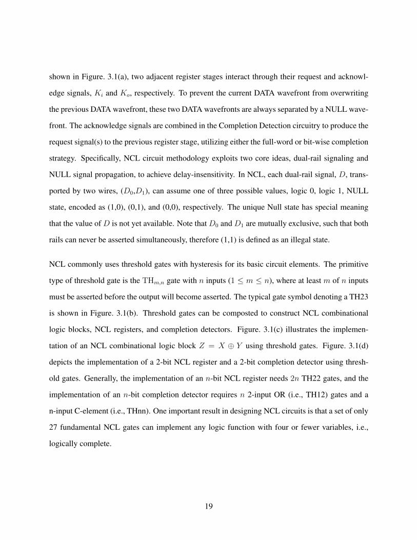
shown in Figure. 3.1(a), two adjacent register stages interact through their request and acknowl-
edge signals, Ki and Ko, respectively. To prevent the current DATA wavefront from overwriting
the previous DATA wavefront, these two DATA wavefronts are always separated by a NULL wave-
front. The acknowledge signals are combined in the Completion Detection circuitry to produce the
request signal(s) to the previous register stage, utilizing either the full-word or bit-wise completion
strategy. Specifically, NCL circuit methodology exploits two core ideas, dual-rail signaling and
NULL signal propagation, to achieve delay-insensitivity. In NCL, each dual-rail signal, D, trans-
ported by two wires, (D0,D1), can assume one of three possible values, logic 0, logic 1, NULL
state, encoded as (1,0), (0,1), and (0,0), respectively. The unique Null state has special meaning
that the value of D is not yet available. Note that D0 and D1 are mutually exclusive, such that both
rails can never be asserted simultaneously, therefore (1,1) is defined as an illegal state.
NCL commonly uses threshold gates with hysteresis for its basic circuit elements. The primitive
type of threshold gate is the THm,n gate with n inputs (1 ≤ m ≤ n), where at least m of n inputs
must be asserted before the output will become asserted. The typical gate symbol denoting a TH23
is shown in Figure. 3.1(b). Threshold gates can be composted to construct NCL combinational
logic blocks, NCL registers, and completion detectors. Figure. 3.1(c) illustrates the implemen-
tation of an NCL combinational logic block Z = X ⊕ Y using threshold gates. Figure. 3.1(d)
depicts the implementation of a 2-bit NCL register and a 2-bit completion detector using thresh-
old gates. Generally, the implementation of an n-bit NCL register needs 2n TH22 gates, and the
implementation of an n-bit completion detector requires n 2-input OR (i.e., TH12) gates and a
n-input C-element (i.e., THnn). One important result in designing NCL circuits is that a set of only
27 fundamental NCL gates can implement any logic function with four or fewer variables, i.e.,
logically complete.
19

Why All Spin Torque Null Convention Logic
Among the types of NCL, the static NCL gate implementation provide a good solution with faster
and more reliable operation. The conventional static NCL gate is shown in Fig. 3.3 (b). The
typical static NCL gate comprised of 4 transistor networks: SET, RESET, HOLD0, HOLD1. The
active and hold function is implemented in CMOS. From given TH gate functionality, the SET and
HOLD1 function of NCL static gate with n inputs can be expressed as:
HOLD1 = I1 + I2 + · · ·+ In
Z = SET + (Z− ×HOLD1)
(3.1)
where the Z− is the previous output value of static NCL gate and Z is current output value. The
given the RESET function of NCL static gate with n inputs can be expressed as:
Z′= RESET + (Z−
′ ×HOLD0) (3.2)
where the Z ′ is complement of Z, and Z−′ is complement of the previous output value of static
NCL gate. In Fig. 3.1 (b), the TH23 static NCL gate is given. The function of four CMOS networks
is given by:
SET = AB
HOLD1 = A+B
RESET = A′B′
HOLD0 = A′+B
′
(3.3)
However, this delay insensitive NCL gate needs the extra transistors to build HOLD0 and HOLD1
that makes the circuit area inefficient. The hardware cost of NCL circuit is usually approximately
20

1.5 to 2 times larger than conventional synchronous CMOS circuit. For example, in paper of [119],
a number of four stage pipeline 32-bits IEEE single-precision floating-point co-processors are im-
plemented both in synchronous CMOS circuit and asynchronous NCL circuit. The given designs
are using the 1.2V IBM 8RF-LM 130nm CMOS process transistor, which is used to performing
addition, subtraction, and multiplication. The synchronous CMOS circuit consumes 104571 tran-
sistors which is around 1.5 times less than asynchronous NCL circuit consumption, which needs
158059 transistors. The domain wall device devices are considered as replacement of the CMOS
transistor. They have extra-low switch energy, fast switch time, however, their device physics limits
applications of spin torque devices, such as hysteresis switching behaviour. The hysteresis switch-
ing behaviour describes domain wall device transfer characteristics, shown in Fig 4.5 (c). The
domain wall is moving if the input current is larger than positive critical current Ic or negative crit-
ical current−Ic. According to the physics of device, the domain wall with size of 3×20×100nm3
has a critical current density J1c,i = 5.2 × 10¹²A/m2 and J1
c,i = −5.2 × 10¹²A/m2. Therefore,
direct mapping hysteresis requirement of NCL to hysteresis of domain wall device can avoid using
of HOLD state logic function. Furthermore, the special 3D architecture of domain wall device and
memristor can reduce hardware area cost dramatically. The layout of domain devices with control
transistor is shown in Fig. 3.2. From the Fig. 3.2, the two bit domain wall device associated with
access transistor achieves 2X higher area density compare with the single domain wall device.
d1 d2
16λ
10λ
(a)
d1 d2
16λ
10λ
(b)
BL
SL
BL
SL
Figure 3.2: (a). Layout of single domain wall with 2 access transistor. (b). Layout of two bitdomain wall with 3 access transistor.
21

Therefore, we realize that replacement of CMOS NCL with emerging devices though physical
characteristics of emerging devices can achieve approximately 30x and 8x improvements in energy
efficiency and chip layout area.
Proposed All Spin Torque Null Convention Logic
(b)
A
z
B
C
B C C
A B
B C C
A B A B C
(a)
Hold0Reset
Hold1Set
Figure 3.3: (a) TH23 static NCL gates. (b) TH23 DWL NCL gate.
In Fig. 3.3, the proposed all spin torque convention logic architecture is presented. It is obviously
to see that large numbers of the transistor are used to keep delay-insensitive performance in con-
ventional static NCL gate, shown in Fig. 3.3. On the contrast, in Fig. 3.3 (b), the DWL NCL
gate only takes several components, whose size are smaller than a single transistor. So that, our
proposed domain DWL NCL gate which is employing domain wall device with hysteresis char-
acter to achieve delay intensive performance has small area than the conventional method. In our
method, domain wall NCL gate employs memristors whose conductance can be precisely modu-
lated by charge or flux through it can be used to implement DWL NCL. The weighted current can
be generated through different programmed memristor by constants Vdd, Vddmi,jd
. The sum of analog
22

current is obtained through connecting in parallel of input based on Kirchhoff’s Current Law with
I-V resistor, which is implemented by domain wall device. The Fig. 5.2 (a) shows architecture of
proposed DWL NCL gate. The inputs binary are represented by V1, · · ·Vn with Vdd is 1 and GND
is 0, receptively. The sum of the input current depends on the number of inputs is equal to 1. So
that, the larger number of input is 1, the larger sum of the input current is obtained to inject to
domain wall logic device. The hysteresis of NCL logic can be also implemented by domain wall
device through critical current and NULL module memristor.
In Fig. 5.2 (c), the waveform of proposed DWL NCL is shown. In steady domain, the difference
of sum of writing current and NULL current is roundly equal or less critical current, therefore, the
domain wall is not moving. When sum of input current is increasing with more number of the
input binary bit is 1, the difference of sum of writing current and null current is roundly more than
critical current, therefore, domain wall is moving by constant velocity, shown in DATA domain.
For the sensing of DW position, we use separated read and write path for reliable issue. The
constants supplied voltage is given at Vpa and Vpb and needed access transistor for sensing opera-
tion. The different clock signals are also needed to control different sensing of NCL gates. These
techniques are required delay element for different NCL gate layer. For example, if a TH23 gate
receives output from a TH44 gate, the sensing clock of TH44 is active at 1ns delay after data arrives
at TH44. The sensing clock of TH23 at 1ns delay after TH44 sensing clock. The same scheme of
C-element asynchronous circuit is proposed by Zianbetov [121]. According to domain wall posi-
tion, the reference is in 2.5KΩ and given largest sensing margin between Vpa and Vpb is v 350mV .
Therefore, we set Vpa and Vpb as 50mV and −50mV in order to keep a good sensing margin. At
the NULL domain, the inputs are all 0, therefore, the difference of sum of writing current and null
current is roundly more than resetting critical current. The domain wall is moving back to initial
position and ready to receive next calculation.
23

Transformation From Boolean NCL to Spin Torque NCL
In the previous section, the architecture of memristor with domain wall logic is proposed to gen-
erating different combination of weights and threshold from NCL boolean logic. Therefore, the
transformation of NCL boolean logic to DWL NCL circuit has to be considered. The algorithm of
generating different inputs memristance and NULL module memristance is proposed in Algorithm
1. With helping of Algorithm 1, The weights and threshold of boolean NCL function are mapped
to DWL device associated with memrisitance and critical current value. Before we introduce the
algorithm, some default definitions and values have to be declared, which is shown in step 1 − 8
in Algorithm 1. The given boolean NCL netlist G is input to the algorithm. The index of i, j indi-
cates different NCL gates and different input of individual NCL gate. Given Vdd is used to generate
different weighted current through memristor. Ti and wi,j are written by the function of Thres(G)
and Weigh(G), which is used to read the logic threshold and weight of individual NCL gate from
given boolean NCL netlist. The calculated memristance of input mi,j and NULL module Mi are
the output of Algorithm 1, which is constrained in range ofmmin andmmax. The value ofmmin and
mmax is obtained from memristor device, in our case, range is from 100Ω to < 38000Ω. The two
domain wall device critical current densities are used to achieve hysteresis of NCL. The domain
wall device critical current density Jc, i1 and J2c,i for each NCL gate is given by measurement of
DW device [43]. The domain wall device critical current density J2c,i = 6.2×10¹²A/m2 will cause
domain wall moving with 20m/s velocity. On another side, current density J1c,i = 5.2×10¹²A/m2
will cause domain wall moving with 0m/s velocity. The critical current I1c,i and I2
c,i are calculated
by injection area and critical current density. In order to explain the algorithm clearly, we consider
two the boolean NCL gates TH23W2 and TH44 with function of f = A + BC, f = ABCD as
example, respectively. For boolean NCL function f = A + BC, three inputs weights are (2,1,1)
with threshold is 2. Since the weights of each input is different with each other, therefore, the al-
gorithm from step 19− 27 are used. By given those conditions, the three input and NULL module
24

memristance values are calculated for function f = A + BC as follows, the sequent of memris-
tance A, B, C is m1,1,m1,2,m1,3.
Case 1: Hysteresis-set 1:
The sum of input current is smaller than threshold and not making domain wall moving, therefore,
Vddm1,2− Vdd
M1< I1
c,1 and Vddm1,3− Vdd
M1< I1
c,1 are both true.
Case 2: Set 1:
The sum of input current is larger than threshold value make domain wall moving, therefore,
2 · Vddm1,2− Vdd
M1> I2
c,1 and Vddm1,1− Vdd
M1> I2
c,1 are both true.
Case 3: Hysteresis-set NULL:
The sum of input current is larger than negative threshold and not making domain wall moving
back, therefore, Vddm1,2− Vdd
M1> −I1
c,1 , and Vddm1,1− Vdd
M1> −I1
c,1 are both true.
Case 4: NULL:
The sum of input current is zero and making domain wall moving back to initial position, there-
fore, −VddM1
< −I2c,1 is true.
The possible memristance of 3 different inputs and Null module are given by equation above.
with Vdd is equal to 0.3V The memrsiatnce of input A is mi,A = 608Ω, memrsiatnce of input
B is mi,B = 1209, memrsiatnce of input C is m1,C = 1209Ω, memrsiatnce of Null module is
Mi = 1209Ω, receptively. For the TH44 gate f = ABCD, the method is similar with above, the
memrsiatnce of input A is mi,A = 2418Ω, memrsiatnce of input B is mi,B = 2418Ω, memrsiatnce
of input C is mi,C = 2418Ω, memrsiatnce of input D is mi,D = 2418Ω, memrsiatnce of Null
module is Mi = 1209Ω.
The algorithm is applying to 27 typical TH gate truth tables, in order to verify results. This algo-
rithm shows that the TH gate can be classified into 5 different groups according to its threshold.
The parameter of domain wall device is based on paper [43].
25

0 10 20 30 400
10
(a) Input A
Cu
rren
t (µ
A)
0000 0001 0011 0111 1111 0111 0011 0001 0000
0 10 20 30 400.00
0.50
(b) Input B
Cu
rren
t (µ
A)
0000 0001 0011 0111 1111 0111 0011 0001 0000
0 10 20 30 400.00
0.50
(c) Input C
Cu
rren
t (µ
A)
0000 0001 0011 0111 1111 0111 0011 0001 0000
0 10 20 30 400.00
0.50
(d) Input D
Cu
rren
t (µ
A)
0000 0001 0011 0111 1111 0111 0011 0001 0000
0 10 20 30 400
10
20
(f) DW position
Po
siti
on
(n
m)
0000 0001 0011 0111 1111 0111 0011 0001 0000
0 10 20 30 40 0.0
30.0
(g) DW sensing current
Cu
rren
t (µ
A)
0000 0001 0011 0111 1111 0111 0011 0001 0000
Figure 3.4: Simulation of proposed TH44 gate through domain wall logic device.
According to the configuration of this DW device, current density 6.2 × 10¹²A/m2 will cause
domain wall moving with 20m/s velocity, on the contract, current density 5.2 × 10¹²A/m2 will
cause domain wall moving with 0m/s velocity. The results of mapping Algorithm1 is shown in
Table 3.1, Table 3.2, Table 3.3.
According to the results from Table 3.3, we take NCL TH44 gate for example. The DW simulation
is done by software mumax3 with parameters, shown in Table. 3.4. When the sum of input current
which is less or equal to critical current may not cause any movement of the DW.
26

Algorithm 1: Calculating Stochastic weight and threshold algorithmInput : G-Boolean NCL netlistOutput: N -DWL NCL netlist
1 Vdd ← 0.3V
2 S ← 40nm2 // injection area of domain wall
3 Ti ← Thres(G) // read threshold of each node
4 wi,j ←Weigh(G) // read weight of each node
5 mmin ← 100Ω // set minimal memristance
6 mmax ← 38000Ω // set minimal memristance
7 Ic1i ← S · 5.2× 10¹²A/m2 // set critical current density for DW velocity=0
8 Ic2i ← S · 6.2× 10¹²A/m2 // set critical current density for DW velocity=20m/s
9 for i = 1 : N do10 if wi,j = wi,1, · · · ,= wi,ni then11 minimize(mi,j=1:n) // find the minimal memritance of input j=1:n
12 subject to :
13 Ti · Vddmi,j
− VddMi
> Ic2i // set 1
14 (Ti − wi,j) · Vddmi,j
− VddMi
< Ic1i // hysteresis
15 −VddMi
< −Ic2i // null
16Vddmi,j
− VddMi
> −Ic1i // hysteresis
17 mmin < mi,j ,Mi < mmax // device constraint
18 else19 wmin ← findmin(wi,j) // find the minimal boolean weight of input j=1:n
20 mi,j=1:n ← mwmin ·wi,j
wmin// calculate memristance of each input
21 minimize(mwmin ) // find the minimal memritance of input j=1:n
22 subject to :
23 Ti · Vddmwmin
− VddMi
> Ic2i // set 1
24 (Ti − wmin) · Vddmwmin
− VddMi
< Ic1i // hysteresis
25 −VddMi
< −Ic2i // null
26Vdd
mwmin− Vdd
Mi> −Ic1i // hysteresis
27 mmin < mi,j ,Mi < mmax // device constraint
At the time of 4 inputs are high, the sum of current is larger than critical current and move domain
right to terminal T2. Therefore, the different combinations of inputs can make domain wall moving
or stepping. The simulation of TH44 gate is shown in Fig. 3.4. The number of inputs is increasing
sequentially to test hysteresis. Before the four inputs are all ones, the different combinations of
input are shown in Fig. 3.4, A = 0, B = 0, C = 0, D = 0, A = 0, B = 0, C = 0, D = 1,
A = 0, B = 0, C = 1, D = 1, , A = 0, B = 1, C = 1, D = 1. At those cases, domain wall is
stepped since the sum of input current and NULL module current are not larger than critical current.
While the four inputs are all active, the sum of the input current and NULL module current is larger
than critical current and making domain wall moving. After the domain wall moves to a specific
position at time duration of all input currents are ones, the active input number is decreasing.
27
Table 3.1: One and two inputs mapping results of proposed Algorithm1 for 27 foundational NCLfunctions
NCL gate Boolean function Weight: Memristance Range(Ω)Threshold
TH12 A+B (1,1:1) mi,A,mi,B ∈ [100,Mi/2];Mi ∈ [100, 1209]
TH13 A+B+C (1,1,1:1) mi,A,mi,B,mi,C ∈ [100,Mi/2];Mi ∈ [100, 1209]
TH14 A+B+C+D (1,1,1:1) mi,A,mi,B,mi,C,mi,D ∈ [100,Mi/2];Mi ∈ [100, 1209]
TH22 AB (1,1:2) mi,A,mi,B,Mi ∈ [100, 1209]TH23 AB+AC+BC (1,1,1:2) mi,A,mi,B,mi,C,Mi ∈ [100, 1209]
TH23W2 A+BC (2,1,1:2) mi,A ∈ [100,Mi/2];mi,B,mi,C,Mi ∈ [100, 1209]
TH24 AB+AC+AD (1,1,1,1:2) mi,A,mi,B,mi,C ∈ [100, 1209]+BC+BD+CD mi,D,Mi ∈ [100, 1209]
TH24W2 A+BC (2,1,1,1:2) mi,A ∈ [100,Mi/2];+BD+CD mi,B,mi,C,mi,D,Mi ∈ [100, 1209]
TH24W22 A+B+CD (2,2,1,1:2) mi,A,mi,B ∈ [100,Mi/2];mi,C,mi,D,Mi ∈ [100, 1209]
At those cases, the domain wall is not moving back to initial position, since an inverse current is
not larger than resetting critical current, the domain wall is still stepped at its current position. At
the time of all inputs are zeros, the sum of the input currents and Null module current is larger than
resetting critical current, and pushing domain wall back to its original position. The simulation
is shown in Fig. 3.4. From the simulation, the hysteresis of NCL logic is implemented through
domain wall hysteresis by using different memristance.
Among the 27 NCL gates, there are 3 special NCL function (TH24comp, THand0, THxor0), which
are not threshold gate [87]. In order to implement these NCL gates, we decompose them to sub
NCL gate. The Fig. 3.5 (a) (b) (c) show architecture of spin-torque-transfer DW device based NCL
(TH24comp, THand0, THxor0) gate.
28

Table 3.2: Two and three inputs mapping results of proposed Algorithm1 for 27 foundational NCLfunctions
NCL gate Boolean function Weight: Memristance Range(Ω)Threshold
TH33 ABC (1,1,1:3) mi,A,mi,B,mi,C ∈ [100, (2/3) ·Mi];Mi ∈ [100, 1209]
TH33W2 AB+AC (2,1,1:3) mi,A ∈ [100, (3/4) ·Mi];mi,B,mi,C ∈ [100, (3/2) ·Mi];
Mi ∈ [100, 1209]TH34 ABC+ABD (1,1,1,1:3) mi,A,mi,B,mi,C,mi,D ∈ [100, (3/2) ·Mi];
+ACD+BCD Mi ∈ [100, 1209]TH34W2 AB+AC (2,1,1,1:3) mi,A ∈ [100, (3/4) ·Mi];
+AD+BCD mi,B,mi,C,mi,D ∈ [100, (3/2) ·Mi]+AD+BCD Mi ∈ [100, 1209]
TH34W3 A+BCD (3,1,1,1:3) mi,A ∈ [100,Mi/2]mi,B,mi,C,mi,D ∈ [100, (3/2) ·Mi]
Mi ∈ [100, 1209]TH34W22 AB+AC (2,2,1,1:3) mi,A,mi,B ∈ [100, (2/3) ·Mi]
+AD+BC+BD mi,C,mi,D ∈ [100, (3/2) ·Mi]; Mi ∈ [100, 1209]
TH34W32 A+BC+BD (3,2,1,1:3) mi,A ∈ [100,Mi/2]; mi,B ∈ [100, (2/3) ·Mi]mi,C,mi,D ∈ [100, (3/2) ·Mi]
Mi ∈ [100, 1209]
The proposed architecture is based on the decomposition of NCL function set. For example, the
NCL gate THxor0 can be decomposed to two layers architecture that consists of 2 TH22 gates
and 1 TH21 gate, shown in Fig. 3.5 (d). The NCL gate THand0 can be decomposed to two layers
architecture that consists of 3 TH22 gates and 1 TH21 gate, shown in Fig. 3.5 (e). The NCL gate
TH24comp can be decomposed to two layers architecture that consists of 2 TH21 gates and 1
TH22 gate, shown in shown in Fig. 3.5 (f). The simulations of different proposed NCL gate are
simulated in Fig. 3.5 (g) (h) (i), respectively. The active input number is increasing sequentially.
For THxor0 gate, at the time of inputs of C and D are active, the DW device for input C and D is
shifting because input current is higher than critical current of DW device.
29

Table 3.3: Four and five inputs mapping results of proposed Algorithm1 for 27 foundational NCLfunctions
NCL gate Boolean function Weight: Memristance Range(Ω)Threshold
TH44 ABCD (1,1,1,1:4) mi,A,mi,B,mi,C,mi,D =∈ [100, 2 ·Mi]Mi ∈ [100, 1209]
TH44W2 ABC+ABD (2,1,1,1:4) mi,A,Mi ∈ [100, 1209]+ACD mi,B,mi,C,mi,D ∈ [100, 2 ·Mi]
TH44W3 AB+AC+AD (3,1,1,1,4) mi,A ∈ [100, (2/3) ·Mi]mi,B,mi,C,mi,D ∈ [100, 2 ·Mi]
Mi ∈ [100, 1209]TH44W22 AB+ACD (2,2,1,1:4) mi,A,mi,B,Mi ∈ [100, 1209]
+BCD mi,C,mi,D ∈ [100, 2 ·Mi]TH44W322 AB+AC (3,2,2,1:4) mi,A ∈ [100, (2/3) ·Mi]
+AD+BC mi,B,mi,C,Mi ∈ [100, 1209]mi,D ∈ [100, 2 ·Mi]
TH54W22 ABC+ABD (2,2,1,1:5) mi,A,mi,B ∈ [100, (5/4) ·Mi]mi,C,mi,D ∈ [100, (5/2) ·Mi]
Mi ∈ [100, 1209]TH54W32 AB+ACD (3,2,1,1:5) mi,A ∈ [100, (5/4) ·Mi]
mi,B ∈ [100, (5/4) ·Mi]mi,C,mi,D ∈ [100, (5/2) ·Mi]
Mi ∈ [100, 1209]TH54W322 AB+AC (3,2,2,1:5) mi,A ∈ [100, (5/6) ·Mi];
+BCD mi,B,mi,C ∈ [100, (5/4) ·Mi]mi,D ∈ [100, (5/2) ·Mi]
Mi ∈ [100, 1209]
Sequentially, the sum of injection current from AB and CD to DW device on the second layer
is higher than second DW critical current. Therefore, second layer DW device is shifting and
producing a high voltage output. Since sensing currents of both DW device are set to 30µA to
keep a good amount of sensing margin, the current inject to the second layer DW device is very
small to achieve TH gate operation with hysteresis.
30

2
1
2
A
B
CD
F
F=AB+CD
1
2
1
A
B
CD
F
F=AC+BC+AD+BD
2
1
2
A
B
C
D
F
F=AB+BC+AD
2
(a) (b) (c)
(g)
(e) (f)(d)
(h) (i)
Figure 3.5: (a) CMOS NCL THXOR gate (b) CMOS NCL THand0 gate (c) CMOS NCLTH24comp gate (d) Spin-torque-transfer DW device based NCL THXOR gate architecture (e)Spin-torque-transfer DW device based NCL THand0 gate architecture (f) Spin-torque-transferDW device based NCL TH24comp gate architecture (g) Simulation of Spin-torque-transfer DWdevice based NCL THXOR gate architecture (h) Simulation of Spin-torque-transfer DW devicebased NCL THand0 gate architecture (i) Simulation of Spin-torque-transfer DW device based NCLTH24comp gate architecture
31
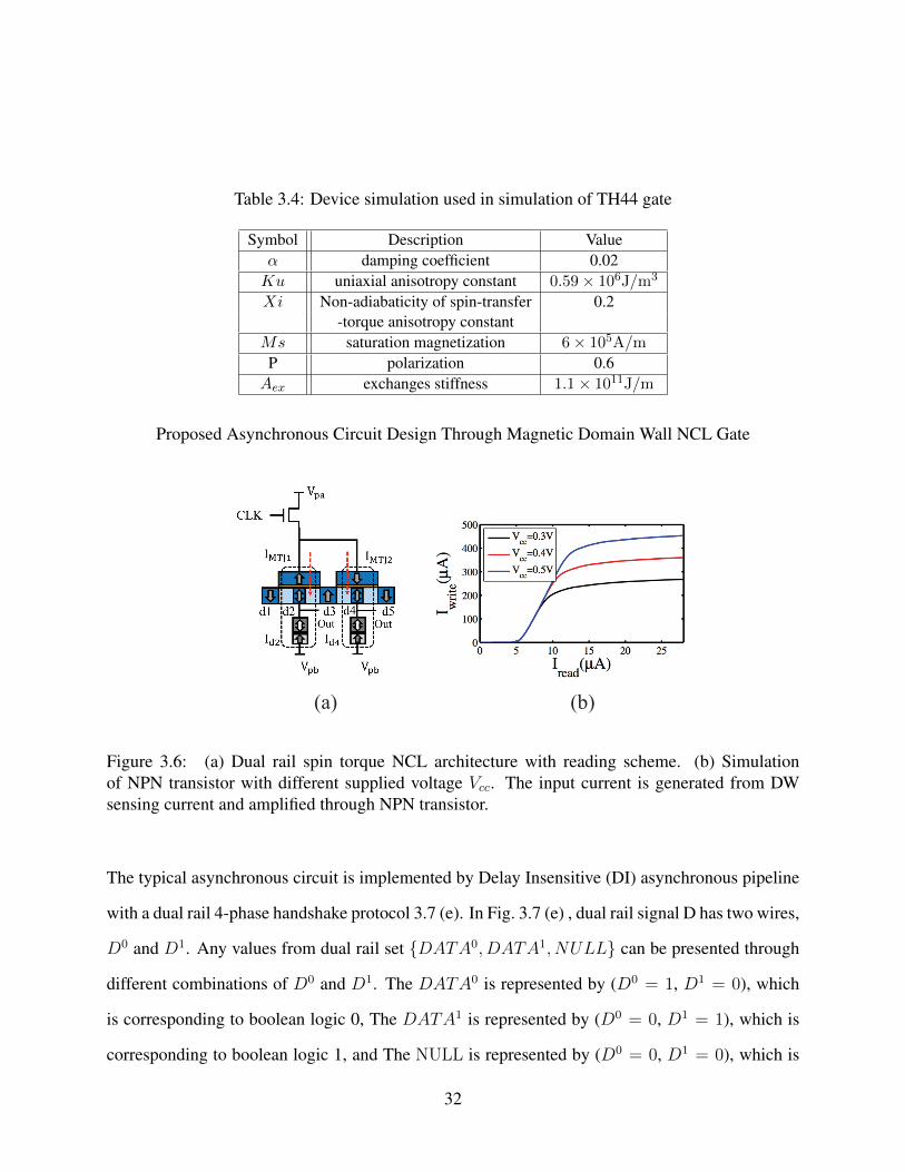
Table 3.4: Device simulation used in simulation of TH44 gate
Symbol Description Valueα damping coefficient 0.02Ku uniaxial anisotropy constant 0.59× 10⁶J/m3
Xi Non-adiabaticity of spin-transfer 0.2-torque anisotropy constant
Ms saturation magnetization 6× 10⁵A/m
P polarization 0.6Aex exchanges stiffness 1.1× 10¹¹J/m
Proposed Asynchronous Circuit Design Through Magnetic Domain Wall NCL Gate
(a) (b)
Figure 3.6: (a) Dual rail spin torque NCL architecture with reading scheme. (b) Simulationof NPN transistor with different supplied voltage Vcc. The input current is generated from DWsensing current and amplified through NPN transistor.
The typical asynchronous circuit is implemented by Delay Insensitive (DI) asynchronous pipeline
with a dual rail 4-phase handshake protocol 3.7 (e). In Fig. 3.7 (e) , dual rail signal D has two wires,
D0 and D1. Any values from dual rail set DATA0, DATA1, NULL can be presented through
different combinations of D0 and D1. The DATA0 is represented by (D0 = 1, D1 = 0), which
is corresponding to boolean logic 0, The DATA1 is represented by (D0 = 0, D1 = 1), which is
corresponding to boolean logic 1, and The NULL is represented by (D0 = 0, D1 = 0), which is
32

corresponding to an empty set. Although the two rails are efficiently implemented delay intensive,
the extra logic cost is the main drawback of dual rail NCL system. The dual rail NCL system
contains at least two DI registers, one at both input and output side 3.7 (f). The multi-pipelined
NCL system can be implemented by inserting additional DI registers. Two adjacent registers are
connected through their request and acknowledge signals, named Ki and Ko, respectively. The
purpose of using these signal is preventing DATA signal not overwriting, and always separated by
NULL signal. The acknowledge signals are used in completion detection module to generate re-
quest signals to previous stage. Since the dual rail set is implemented by separate logic, the double
usage of hardware causes area usage inefficient. The Fig. 3.7 (a) shows proposed architecture of
DWL dual rail NCL. The two adjacent domain wall devices with same resistance in are connected
with shared terminal, which is injected by NULL module current. The two other terminals are
injected by the different current sum of inputs combinations. Usually, one side is injected by the
current sum of D0, another side is injected by the current sum of D1. The resistance of vertical
write current path for left Rl and Rr right side domain wall are same and given by [42]. In order to
explain operation of proposed DWL dual rail NCL architecture, the equivalence analog circuits of
proposed DWL dual rail architecture is shown in Fig. 3.7 (b), (c), (d). In Fig. 3.7 (b), the NULL
case happens at two input combinations. When the inputs are all zero, V 0sum = 0 and V 1
sum = 0,
Vnull is larger, thus, the two currents with opposite direction are created. If we set current direction
from NULL to input terminal is positive direction, the combinations of sum of input current and
NULL module current is smaller than negative critical current, therefore, moving back to initial
positions. In Fig. 3.7 (c), the input vector V 00 · V 0
n has smaller voltage than NULL module supplied
voltage Vnull, therefore, the domain wall device for input Vsum0 is not moving. On another side,
the input vector V 10 · V 1
n has higher voltage than NULL module supplied voltage Vnull, therefore,
the domain wall device for input Vsum1 is moving. In Fig. 3.7 (d), the input vector V 00 · V 0
n has
higher voltage than NULL module supplied voltage Vnull, therefore, the domain wall device for
input Vsum0 is moving. On another side, the input vector V 10 · V 1
n has smaller voltage than NULL
33

module supplied voltage Vnull, therefore, the domain wall device for input Vsum1 is not moving.
For reading domain wall position of proposed architecture, it is more critical since two device wall
device is connecting together. Therefore, the proposed architecture has 4 different level of reading.
The Fig. 3.6 (a) shows dual rail spin torque NCL architecture with reading scheme. In Fig. 3.6 (a),
series of domain d1 to d5 are associated with two fixed magnets MTJ on top. As mentioned earlier,
the two free domains d2 and d4 can be written to parallel and anti-parallel to MTJ magnetization in
order to store ‘0‘ or ′1′. The separated read-write operation and path can make higher oxide thick-
ness in the architecture, which is creating high TMR and larger reading margins [96]. Although the
paper of Sharad [96] proposed new device structure for similar multi-domain wall architecture, in
order to distinguish two the two resistance states of two domain wall devices, our method choose
a vertical reading path and npn-transistor to achieve accuracy reading operation without making
the different effective area of two domain wall. Read disturb margin is defined as the difference
of reading current passing through the different domain wall region during reading operation. The
Table. 3.5 shows read current values for four states of proposed dual rail NCL architecture. The
peak values of transient read current with a thickness of free layer tox = 1.6nm and pulse duration
of 0.5ns. Here Im1 and Im2 denote the currents passing through two MTJs, the parallel MTJ state
produce higher current and the anti-parallel MTJ state produce lower current. The Id2 and Id4 rep-
resents current passing through two free domains d2 and d4 respectively. In Table3.5, two levels
of reading current will produce during the reading operation. The NPN transistor transmits these
current to next stage. There are two purposes of NPN transistor. The first one is amplifying since
the domain wall reading current is very small and less than 30µA to keep accuracy reading margin.
The second reason is threshing, the reading current of anti-parallel state will not produce current
to next stage, because of NPN transistor threshold, shown in Fig.3.6. If both of domain wall states
are anti-parallel, the zero current of Id2 and Id4 are generated to representing NULL state of NCL
logic. The two parallel domain wall states are invalid according to NCL dual rail encoding.
34

Table 3.5: Read current values for four states of proposed dual rail NCL architecture
Current
Domain WallState d2 : P
d4 : APd2 : APd4 : P
d2 : Pd4 : P
d2 : APd4 : AP
Im1(µA) 15.8 4.1 16.7 invalidIm2(µA) 3.2 15.7 14.4 invalidId2(µA) 16.3 4.6 1.4 invalidId4(µA) 3.9 14.9 0.9 invalid
In order to exam proposed DWL dual rail logic, one bit NCL full adder is implemented. In Fig. 3.8
(b), the one bit full adder employs double TH23 and TH34W2 gate to implement DATA0 and
DATA1. The schematic of one bit full adder is shown in Fig. 3.8 (b), where X and Y are input
addends and C is carry input. The optimized circuit is obtained through TCR method [100], and
the carry out is given byC0o = X0Y 0+C0X0+C0Y 0, C1
o = X1Y 1+C1X1+C1Y 1, S0 = X0Co1 +
C1oY
0 + C1oC
0 + X0Y 0C0, and S1 = X1Co0 + C0
oY1 + C0
oC1 + X1Y 1C1. Therefore, the one bit
full adder can be implemented through four TH NCL gates, TH34W2 and TH23 gates. Although,
the paper [100] try to reduce transistor size by TCR optimization, the area and power consumption
are still drawbacks of widely used asynchronous circuits system. The Fig. 3.8 (a) shows proposed
DWL-NCL implementation of one bit full adder. The two TH23 NCL gates are implemented by
two domain wall device connected through share terminal and similarly to TH34W2 gate. The
operation of DWL for dual rail architecture is as same as previous proposed single static DWL
NCL gate. However, the mapping algorithm has a little bit changes, since the Null module current
should be calculated through two different input combinations. The simulation is implemented as
same parameter set up with previous TH44 gate and shown in Fig. 3.9. The simulation has several
different input combinations to generate the accuracy results.
35

LogicREG REG
ACK
(a)
ACK
Logic 1 Logic 0Null
Output: 00 (NULL) Output: 01 (DATA=1) Output: 10 (DATA=0)
(b) (c) (d)
(e)
(f)
… …
… …
Figure 3.7: (a). DWL duail rail NCL implementation, the two dual rail bits can be implementedthrough two domain wall device which is separated by shared terminals. (b). The equivalenceanalog circuit of proposed DWL duail rail architecture in NULL case. (c). The equivalence analogcircuit of proposed DWL duail rail architecture in DATA 1 case . (d).The equivalence analogcircuit of proposed DWL duail rail architecture in DATA0 case. (e). The DWL dual rail 4-phasecommunication protocol. (f). DWL asynchronous QDI pipeline architecture, the input is controlledby local handshaking and completion detection signal (ACK).
(a) (b)
Figure 3.8: (a). DWL duail rail NCL architecture of one bit full adder. (b). CMOS duail rail NCLarchitecture of one bit full adder.
36

0.0 0.5 1.0 1.5 2.0 2.5 3.0 3.5 4.0 4.50.0
2.0
4.0
(a) Input A0
Curr
ent (µ
A)
0 0 0 0 0 1 0 0 0
0.0 0.5 1.0 1.5 2.0 2.5 3.0 3.5 4.0 4.50.0
2.0
4.0
(b) Input A1
Curr
ent (µ
A)
0 1 0 1 0 0 0 1 0
0.0 0.5 1.0 1.5 2.0 2.5 3.0 3.5 4.0 4.50.0
2.0
4.0
(c) Input B0
Curr
ent (µ
A)
0 0 0 1 0 0 0 0 0
0.0 0.5 1.0 1.5 2.0 2.5 3.0 3.5 4.0 4.50.0
2.0
4.0
(d) Input B1
Curr
ent (µ
A)
0 1 0 0 0 1 0 1 0
0.0 0.5 1.0 1.5 2.0 2.5 3.0 3.5 4.0 4.50.0
2.0
4.0
(f) Input Cin0
Curr
ent (µ
A)
0 1 0 1 0 0 0 0 0
0.0 0.5 1.0 1.5 2.0 2.5 3.0 3.5 4.0 4.50.0
2.0
4.0
(g) Input Cin1
Curr
ent (µ
A)
0 0 0 0 0 1 0 1 0
0.0 0.5 1.0 1.5 2.0 2.5 3.0 3.5 4.0 4.5
20
(h) DW Sout,0
Positio
n (
nm
)
0 1 0 0 0 1 0 0 0
0.0 0.5 1.0 1.5 2.0 2.5 3.0 3.5 4.0 4.5
20
(i) DW Sout,1
Positio
n (
nm
)
0 0 0 1 0 0 0 1 0
0.0 0.5 1.0 1.5 2.0 2.5 3.0 3.5 4.0 4.5
20
(j) DW Cout,0
Positio
n (
nm
)
0 0 0 1 0 0 0 0 0
0.0 0.5 1.0 1.5 2.0 2.5 3.0 3.5 4.0 4.5
20
(k) DW Cout,1
Positio
n (
nm
)
0 1 0 0 0 1 0 1 0
Figure 3.9: Simulation of proposed DWL NCL full adder.
The Performance Analysis and Discussion
In this section, we compare performance of proposed design at gate and system level. In gate
level, we simulate proposed TH44 NCL gate. For proposed TH44 NCL gate architecture, the
MTJ resistant is calculated by length of free layer (100nm), width of free layer W, DW position
x (middle point), RAAP , RADW , and RAP are MTJ resistant area product for anti-parallel, DW,
37
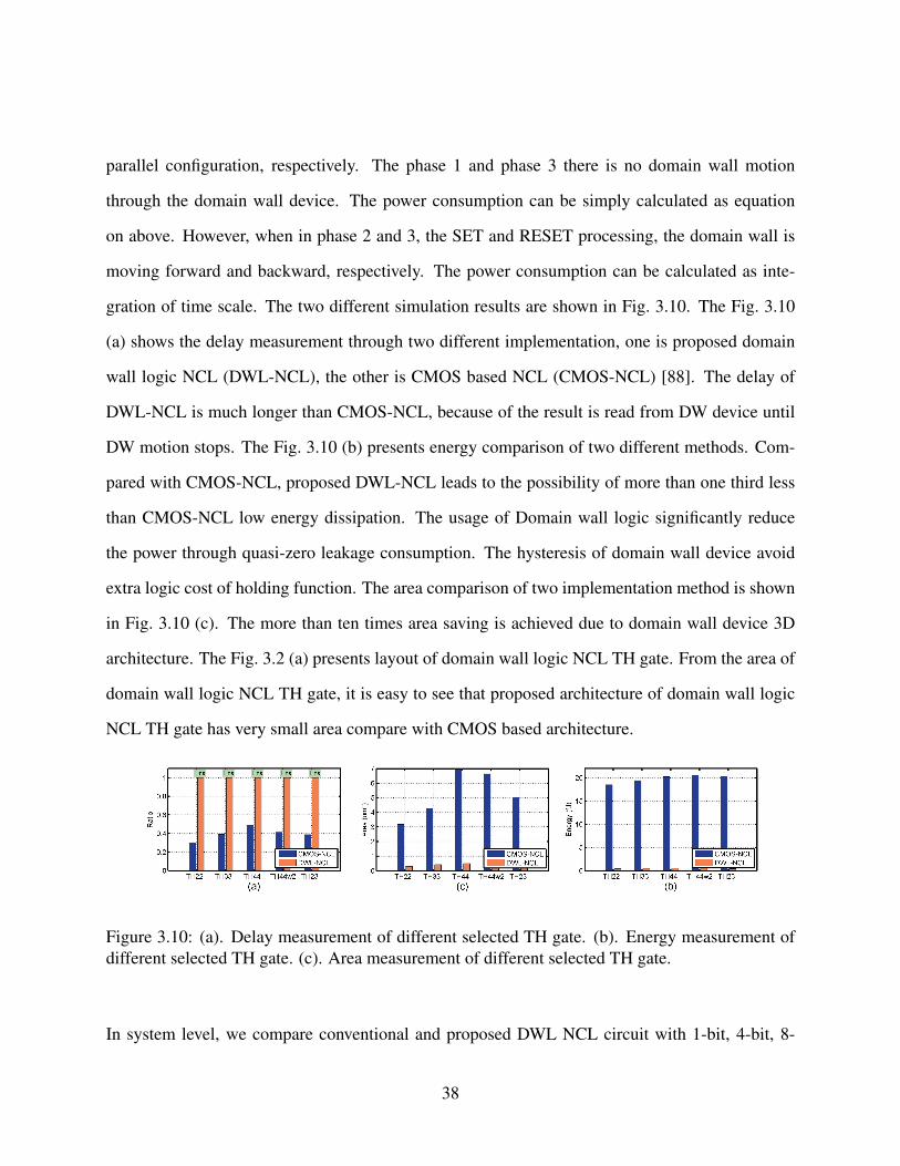
parallel configuration, respectively. The phase 1 and phase 3 there is no domain wall motion
through the domain wall device. The power consumption can be simply calculated as equation
on above. However, when in phase 2 and 3, the SET and RESET processing, the domain wall is
moving forward and backward, respectively. The power consumption can be calculated as inte-
gration of time scale. The two different simulation results are shown in Fig. 3.10. The Fig. 3.10
(a) shows the delay measurement through two different implementation, one is proposed domain
wall logic NCL (DWL-NCL), the other is CMOS based NCL (CMOS-NCL) [88]. The delay of
DWL-NCL is much longer than CMOS-NCL, because of the result is read from DW device until
DW motion stops. The Fig. 3.10 (b) presents energy comparison of two different methods. Com-
pared with CMOS-NCL, proposed DWL-NCL leads to the possibility of more than one third less
than CMOS-NCL low energy dissipation. The usage of Domain wall logic significantly reduce
the power through quasi-zero leakage consumption. The hysteresis of domain wall device avoid
extra logic cost of holding function. The area comparison of two implementation method is shown
in Fig. 3.10 (c). The more than ten times area saving is achieved due to domain wall device 3D
architecture. The Fig. 3.2 (a) presents layout of domain wall logic NCL TH gate. From the area of
domain wall logic NCL TH gate, it is easy to see that proposed architecture of domain wall logic
NCL TH gate has very small area compare with CMOS based architecture.
Figure 3.10: (a). Delay measurement of different selected TH gate. (b). Energy measurement ofdifferent selected TH gate. (c). Area measurement of different selected TH gate.
In system level, we compare conventional and proposed DWL NCL circuit with 1-bit, 4-bit, 8-
38

bit, 16-bit, 32-bit full adder. The conventional NCL full adder is followed architecture shown in
Fig.3.8 (b). The circuit is implemented and simulated using IBM SOI1250 45nm CMOS process
standard cell library. The simulation is using nominal power supply voltage of 0.92V , temperature
27C, and capacitive load of 10fF. The proposed DWL is using the parameter in Table. 3.4. In
Fig.3.11 (a) we analysis the delay of two different implementation. The proposed DWL has more
delay than CMOS adder, since the velocity of DW moving is around 20m/s. Our programming
algorithm may improve the delay performance through adjusting device threshold to create larger
writing current, which is making high velocity. In our case, we use Jc2i = 6.2×10¹²A/m2 which is
making DW moving with 20m/s. Since the full adder is fully pipelining with bit increasing, delay
of full adder is not changing with bit increasing. In Fig.3.11 (b), we compare energy consumption
of two different implementation. Our proposed circuit is running under very low operation current,
only few µW for memristors, 0.15µW for sensing unit and few µW fro DW device. The Fig.3.11
(b) shows power saving in log scale. The proposed DWL full adder achieve 20X times energy
saving for 32bit fulladder. In Fig.3.11 (c), the area comparison between CMOS NCL and DWL
NCL full adder. By using 3D structure of proposed dual rail DWL NCL full adder, the area of
proposed full adder is significantly decreasing. Comparing of CMOS NCL full adder, the DWL
NCL full adder achieve 8X times area saving.
Figure 3.11: (a). Delay measurement of NCL full adder with increasing bits. (b). Energy mea-surement in log scale of NCL full adder with increasing bits.(c). Area measurement in log scale ofNCL full adder with increasing bits.
39

Large Scale Application of Proposed NCL Architecture
To compare the proposed architecture with other conventional architecture, a number of four
stages pipelined 32 bit IEEE single-precision floating point co-processor is implemented. The
co-processor consists of several blocks to perform addition, subtraction, and multiplication, shown
in Fig. 3.12. The conventional CMOS-based NCL design is implemented by 1.2V IBM 8RF-LM
130nm CMOS process. The simulation of conventional method is simulated at transistor level
by using Cadence’s UltraSim simulator. The VerilogA library is created through 25 sets of ran-
domly selected floating-point numbers for each add/sub and multiply operation. To validate our
proposed architecture and circuit design method, we implemented same application application
design. Besides verifying its application accuracy, we also quantitatively measure and compare its
performance metrics, such as energy consumption, chip area, and performance, with its counterpart
implemented with the 1.2V IBM 8RF-LM 130nm CMOS process. Before presenting our simula-
tion results, we first present the overall CAD flow of our mixed-model simulations in Fig. 4.17.
There are four essential design steps depicted with gray boxes. For the cognitive application itself,
we take advantage of both the logic synthesis tool and the technology mapping capability of the
Cadence tool chain. Specifically, we start with building a rich cell library of synapses with 27
different NCL gates. Subsequently, these design results will be read by the Cadence Spectre tool,
which creates a SPICE circuit library. Such library will then be used to evaluate the performance
of our DWNCL at gate and system level.
Table. 3.6 shows performance results of different implementation of 32 bit IEEE single-precision
floating point co-processor. The delay of asynchronous designs is calculated by average DATA+NULL
processing time. For synchronous design, we calculated by maximum speed operating clock. In the
Table. 3.6, the results of conventional NCL implementation using Low-Vt and High-Vt transistor
are presented. Number of these designs is highest among all designs listed in Table. 3.6.
40
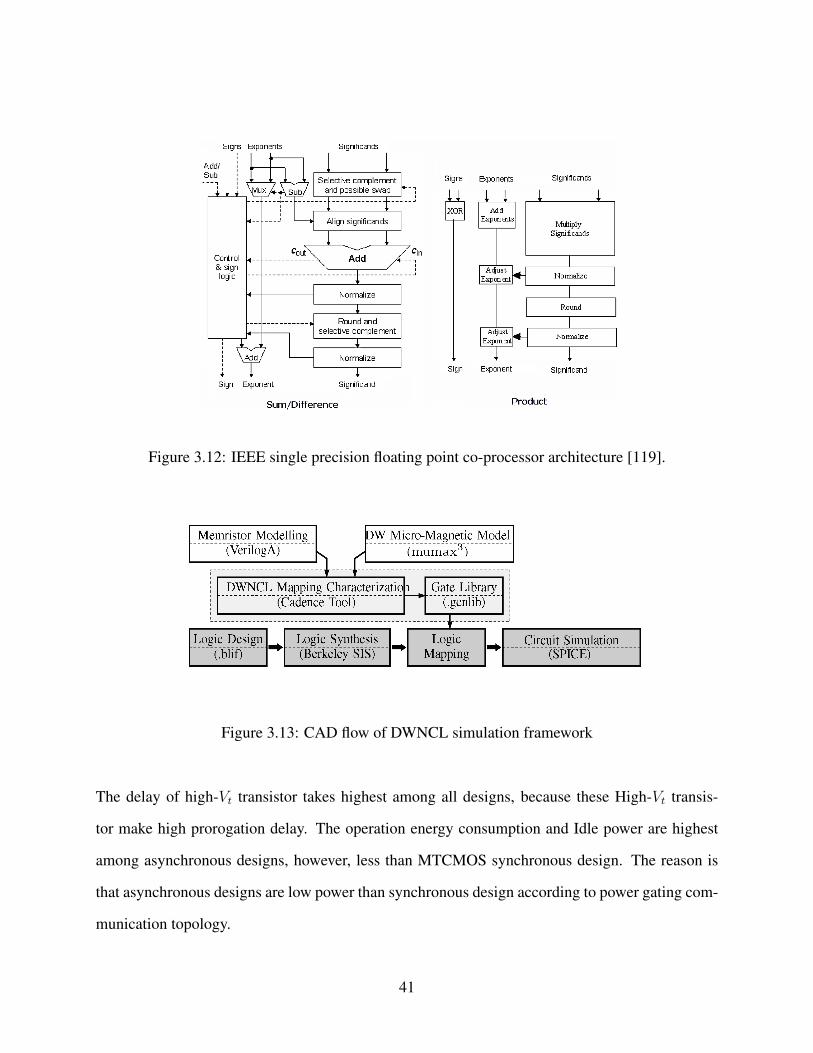
Figure 3.12: IEEE single precision floating point co-processor architecture [119].
Figure 3.13: CAD flow of DWNCL simulation framework
The delay of high-Vt transistor takes highest among all designs, because these High-Vt transis-
tor make high prorogation delay. The operation energy consumption and Idle power are highest
among asynchronous designs, however, less than MTCMOS synchronous design. The reason is
that asynchronous designs are low power than synchronous design according to power gating com-
munication topology.
41

Design Type #Delay Operation Energy Idle Power
Transistors(ns) (pJ) (nW)
Add/Sub. Multi. Add/Sub. Multi. Add/Sub. Multi.NCL Low-Vt 158059 14.1 14.4 27.4 23.7 12300 12300NCL High-Vt 158059 32.7 33.4 28.5 25.1 208 208
MTCMOS 104571 10 13.9 124.3 124.7 156000 132000Synchronous
SMTNCL1 SECII 119244 10.7 15.4 14.6 26 121.1 121.1SECII
DWNCL 18801 34.77 35.14 0.876 1.03 11.254 12.22
Table 3.6: Comparison of different design implementation for 32 bit IEEE single-precision floatingpoint co-processor [119].
For MTCMOS synchronous design, although it takes less number of transistor compare to most of
asynchronous designs, operation energy consumption and idle power are highest in the Table. 3.6,
because MTCMOS design only sleep after a preset number of inputs [104]. Among asynchronous
designs, SMTNCL1 SECII design has less transistor number, delay, and power consumption, be-
cause of new sleep mode. The proposed sleeping completion logic implemented with the C/L
can reduce area, energy, and leakage power [101]. Compare to all asynchronous and synchronous
design, our proposed DWNCL design has two orders less transistor number, 10X less operation
energy and idle power, however, 3X more delay. The using of memristor and DW device makes
less number of transistors, which are majority part of area consumption compare to memristor
and DW device size. The DATA process takes two parts of energy consumption, programming
and sensing. An average of ∼ 40µA current flows through memristors. Therefore, programming
energy is calculated to be ∼ 0.5fJ for 1ns writing time. The sensing energy is calculated to be
∼ 2.5fJ for 1ns reading current. For NULL process, the resetting energy is occurred. In our
proposed architecture, an ∼ 50µA current is used to shift DW device in 1ns, which is leading to
∼ 0.75fJ resetting energy.
42

Memristor error analysis
(a) (b)
(c) (d)
Figure 3.14: (a). Memristor refresh architecture, the refresh signal is controlled by inputs of DWreset signal and acknowledge signal from next stage. (b). The waveform of control signal inR/W control module. (c). The memristor drift simulation of different input current with timeincreasing. (d). The memristor drift simulation of different pulse duration current with inputcurrent increasing.
The write procedure accuracy is depend on some of analog components, such as random off-
set comparator, DAC, and current source. The paper of Fan [36] has been proposed analysis of
memristor writing. The more accuracy would entail higher design complexity for these blocks
and lower write speed. The reading accuracy is very important aspect to be considered. When
the memristor has been programmed through writing current, the ions drift for any electric field
across the device and so the memristance changes over time. The analytical model of memristor
43

drift has been validated by linear and non-linear drift velocity model and experiments are tested
in fabricated memristors [108]. The changes of this drift may either from Ron to Roff or Roff to
Ron, depend on the polarity of applied voltage. There are two parameters effect on memristance
changes due to drift model, applied voltage and time. In this paper, we use the memristor droft
model from paper of [67] and simulating different effect of memristance by increasing of supplied
voltage and time. The real device measurement is also repeated from previous research work [60].
From the Fig. 3.14 (c), with time increasing, the resistance of memristor is changing due to drift
model and the bigger supplied voltage will cause larger changes of resistance. For the Fig. 3.14
(d), with the voltage increasing, resistance of memristor is changing due to drift model and the
longer pulse duration will cause larger changes of resistance. In order to overcome this drift is-
sue, there are two kinds of options can be considered. One is device level options, another one is
memristance refresh. The device level options are focus on device fabrication with 36nm of thick
titanium dioxide between a 9 nm titanium electrode at the top and 12 nm titanium electrode at
bottom [111]. However, it is very difficult to fabricate and no spice model published, therefore, it
is not a candidate to considered. The memristor refresh method is refreshing memristor to correct
changes causing by memristance drift. The NCL design have the tolerance to allow memristance
drift, beyond which they are refreshed to initial memristance value. Although ideal refreshment
cycles are set to maximum, however, every NCL logic combination has different drift tolerance
to minimized circuit delay. Therefore, the number of data processed that can be applied before a
refresh is needed can be calculated. The Fig. 3.14 (a) shows architecture of proposed memristor
drift refreshment. The architecture is based on memristor R/W control module. The data counter
is inserted to R/W control module to active refresh procedure, when the number of data processed
is exceed to threshold number, which is also meaning that the memristor drift is exceed to design
requirement. The Fig. 3.14 (b) shows the waveform of different control signal in R/W control
module. The multi-pipelined NCL system can be implemented by inserting additional DI regis-
ters. Two adjacent registers are connected through their request and acknowledge signals, named
44

Ki and Ko, respectively. The purpose of using these signal is preventing DATA signal not over-
writing, and always separated by NULL signal. The acknowledge signals are used in completion
detection module to generate request signals to the previous stage. The memristance refresh mod-
ule is active, when request signal is active and threshold counter is reached setting threshold. Since
the special communication scheme of multi-pipelined NCL system, the memristor refreshment
process do not cause any delays.
Domain wall error analysis
The reliability of domain wall device is excellent. The domain wall velocity and critical current
are not sensitive to external magnetic field or temperature [44]. They also make a report of write
endurance for the Co/Ni wire with 10 years retention time at 150 and 1 × 10¹⁴ times write. In
this section, we analysis heating effect on the magnetic-metallic domain wall device. The effect of
Joule heating is simulated in paper of Fan [36]. The conclusion is that thin and shot central free
domain is the most critical portion with current drive heating. In order to reduce effect of Joule
heating effect, the larger contact area of two fixed domains and shorter free domain will be used.
Conclusion
Implemented with the CMOS device technology, many innovative logic circuit design methodolo-
gies, such as threshold logic and NCL, prove to be difficult for wide adoption due to their high
costs. Fortunately, emerging spintronic devices present ample opportunities to innovate in logic
circuit design. This work a first step towards this direction. One valuable lessor we learned from
this study is that the key to the success in using emerging devices for logic circuits is how to
natively exploit the inherent physical property of these emerging devices, instead merely treating
45

them simply as some “super” switches to replace CMOS transistors.
46

CHAPTER 4: DESIGN OF STOCHASTIC ARTIFICIAL NEURAL
NETWORK THROUGH EMERGING DEVICES
Introduction
Motivated by the amazing parallel processing capability of human brain, artificial neural net-
work (ANN) aims at achieving human-like cognitive ability while consuming ultra-low power [35,
34, 32, 33]. Although a great many of different ANN models have been explored and imple-
mented [5, 51, 22], all existing ANN architectures employ neurons as their key computational
units, which are interconnected to each other and to external stimuli through programmable con-
nections based on synapses [5, 51, 37]. Mathematically, the basic operation of individual neuron
can be succinctly abstracted as a weighted sum and a non-linear transfer function, which can be
expressed as Y = f(∑Wi · xi − T ), where Y , xi, Wi, T , and f denote the output of this neu-
ron or activation level, its ith input, its ith synapse weight, its threshold, and its neuron transfer
function, respectively. Despite of its algorithmatic simplicity, a neuron could be challenging to
implement with hardware devices because any reasonably-sized ANN consists of hundreds of neu-
rons densely interconnected through synapses. Specifically, the energy efficiency, performance,
and device density of a hardware ANN is governed by three factors: 1) the circuit design of its
neurons and synapses, 2) its underlying operating principle, 3) its device technology for hardware
implementation. Fig. 4.1 shows the overall architecture of a typical multi-layer artificial neural
network with different transfer functions. There are several notable challenges of implementing an
ANN with hardware that have motivated our study. First, although almost all ANNs share a similar
network topology of neurons, each neuron can have a quite different transfer function, which can
significantly affect the computing capability of a given ANN [82, 84, 28, 62, 70, 57].
47

×
×
×
… ∑
ResetT
Sum Transfer
function
Step
Piecewise
linear
Logistic
sigmoid
Hyperbolic
tangent
Soft limit
y
x0
1y
x0
1
y
x0
1y
x0
1
-1
Figure 4.1: Structure of an artificial neuron. It consists of three computation blocks. The weightedsum of all inputs are passed to its output through a transfer function. Four most common transferfunctions are shown on right side of Fig. 4.1.
In fact, numerous studies have shown that the hard-limiting binary neuron output levels can se-
riously hinder inter-neuron communication. In contrast, soft-limiting neuron transfer functions,
through allowing a continuous range of activation levels between “0” and “1”, can greatly improve
the neural network modeling capability as well as reduce network complexity [37]. Unfortunately,
it is extremely challenging to determine the optimal neuron transfer function for a given input
dataset and network topology. Second, almost all existing ANN hardware implementations are
completely based on deterministic digital or analog operations. However, while being precise and
stable, such operating principles are fundamentally not very tolerant to device variations. Such in-
tolerance poses severe challenges to exploiting emerging device technologies, such as spin-torque-
transfer technology, which are known to possess high device variations. Finally, most prior works
implement ANN neurons and synapses using CMOS, thus typically consuming large numbers of
transistors and high power consumption. However, to fully exploit emerging device technologies
in order to successfully build powerful, yet energy-efficient cognitive computing hardware based
on ANN, novel methodologies of circuit and architecture design have to be developed.
48

Spintronic devices have been considered as an excellent alternative technology to implement brain-
inspired computing architectures because they often operate at ultra-low supply voltage and enjoy
ultra-high device density. However, these emerging devices often exhibit strong stochastic switch-
ing behaviors and suffer from large variations in both electrical characteristics and device relia-
bility. Therefore, how to efficiently leverage the unique device properties of emerging spintronic
devices to facilitate brain-inspired computing tasks becomes an both intriguing and important re-
search challenge. In this paper, we present a stochastic-based soft-limiting artificial neural network
(S-ANN) implemented with the emerging spin-transfer-torque device technology. The S-ANN ar-
chitecture has two innovative features.
• First, we do not attempt to implement the optimal neuron transfer function, but rather pro-
pose an energy-efficient multi-stage pumping circuit with spin-torque-based devices that
implements a continuous non-linear soft-limiting transfer function. Such a signal trans-
formation permits interesting hardware realizations of synapse weighted sum and soft-limit
transfer function.
• Second, our S-ANN is completely stochastic-based, i.e., all signals traversing across its net-
work are just random signals with the signal values encoded as their probability density
functions. Such an stochastic-based computing model has shown to be significantly more
robust than the conventional deterministic model.
Our mix-mode device and circuit level simulation results have shown that, compared with other
digital/analog CMOS-based neural network architecture, our proposed S-ANN can achieve more
than 1.5 orders of magnitude lower energy and 2.5 orders of magnitudes less hidden layer area.
The rest of this paper is organized as follows. In section 4, we investigate prior works on ANN
hardware implementations. Section 4 presents our motivations of adopting stochastic-based method-
49

ology to implement ANN. Section 4 describes theory of stochastic based ANN. Section 4 explains
stochastic switching of MTJ and DWM devices. In Section 4 and 4, we describe in detail the circuit
design of stochastic-based synapse and neuron with spin-torque-transfer (STT) devices, respec-
tively. Section 4 assembles all components and presents the overall architecture of our stochastic-
based artificial neural network (S-ANN). In section 5, we choose an English sentence recognition
as our benchmark application to quantify the performance and energy efficiency of our S-ANN
and compare them with other ANNs with similar capability but implemented with other device
technologies. In section 4, the analytical error study is proposed. Finally, Section 5 concludes this
paper.
Prior Work on ANN Hardware Implementation
Artificial Neural Network
Deterministic Stochastic
Hard limit Soft limit
Con. Em. Em.Con. Con. Em. Con.
Hard limit Soft limit
R. Gadea[6]
E. Ordonez[7]
S. Kung[8]
P. Ienne[9]
A. Ber.[10]
J. Dobes[11]
I.E. Ebong[12]
J. Starzyk[13]
I. Bayr. [14]
C. Alippi. [15]
R. Dlugosz[16]
D. Fan[4]
M. Kolasa[17]
M. Belli[18]
Windecker[19]
G. Palma[20] J. Yuan[21]
T. Kosel[22]
B. Brown[23]
This Work
H. Li[24]
Em.
Figure 4.2: Taxonomy of current ANN designs. Con: CMOS Technology; Em: Emerging DeviceTechnology.
Since its conceptual inception, ANN has attracted significant attention from both academia and
industry. In this paper, we focus mainly on the hardware implementation research of ANN. In
order to provide a high-level perspective of our work, Fig. 4.2 presents one possible taxonomy
50

of some existing hardware implementations of ANN. If categorized by their underlying operating
principles, the majority of ANN hardware implementations follow either deterministic model or
stochastic model. In the deterministic domain, both neuron signals and their operations are deter-
ministic. With digital circuits with CMOS, an ANN implementation normally uses a hard-limit
transfer function, also called step function, because of its binary output states. Possible draw-
backs of digital ANN implementations include large hardware cost (such as multiplication) and
slow operation speed [47, 84, 66, 54, 9]. Therefore, there are surging research works [26, 28, 103]
that explore emerging devices to implement synapse and hard limit transfer functions for a digi-
tal ANN. In addition, soft-limiting transfer function, which has continuous output states, has also
been investigated with conventional CMOS and emerging device technologies [37, 6, 3, 25, 62].
Among them, the most relevant work to ours is a nonlinear soft-limiting neuron that exploits spin
transfer torque [37]. Specifically, this work leverages newly emerging devices such as the Spin
Transfer Torque (STT) device and Domain Wall Motion (DWM) magnetic strip that can efficiently
implement a soft limiting non-linear neural transfer function to achieve more than two orders mag-
nitude lower energy consumption. However, due to the physical nature of STT and DWM devices,
the design in [37] is quite restricted in its transfer function form and synapse range, compared
with its CMOS counterpart. Very recently, a great many researchers started to recognize that
stochastic-based neurons may significantly enhance the capability and stability of a neural net-
works [8, 110, 85, 57, 63, 14, 70]. Although with very encouraging successes, these works have
two potential limitations. First, most of them involved CMOS random number generators to imple-
ment stochastic neurons and synapses [23], thus requiring a large transistor count and high power
consumption. Second, most traditional CMOS-based TRNGs suffer from physical noise, such as
telegraph noise, thermal noise, and oscillator jitter, therefore, extensive post-processing is required
which causes significant performance, power and area overhead.
51

Why Stochastic-based ANN?
There are three main motivations for implementing stochastic-based ANN with emerging devices,
such as STT and DWM technologies. First, suffering from relatively large device variations.
emerging spintronic devices currently can not be simply used as a reliable high-performance alter-
native to replace CMOS device technology. Instead, exploiting their inherent stochastic switching
properties can potentially be quite promising. Second, stochastically computing ANN can enable
much simpler logic operations instead of expensive multiplications and additions typically used in
deterministic ANN. For example, deterministic multiplications can be replaced with simple AND
operations of random samples [82]. Third, computing under stochastic domain has been shown
to be much more robust than deterministic one. In the following, we elaborate on each of these
motivations with more details.
(a) (b)
Figure 4.3: (a) MTJ device resistance histogram distribution of two states RP and RAP underσ/µ = 5%, 10%, and 25% of device resistance (b) Comparison of weight variation on memristorbased method and MTJ stochastic based method
Firstly, almost all emerging devices exhibit strong nonidealities in their device characteristics [60,
13, 115]. In particular, device variations in emerging devices are quite severe [60, 13, 115]. For
example, Rajendran [89] has shown that given constant memristance may drift from 120.47 MΩ
52

to 41.92 MΩ after mere 100 seconds. All these device nonidealities pose fundamental obstacles to
adopting the conventional deterministic logic design methodology. We now use memristor-based
neural network as an illustrative example to demonstrate the negative impact of device variations
if implemented with deterministic principle. Numerous studies have exploited adjustable memris-
tances to implement weighted synapse [89, 37], Unfortunately, not only device variation can lin-
early change the synapse weight, but also memristance drift can significantly change the synapse
weight even when a constant voltage is applied. We now quantitatively demonstrate the negative
impact of device variations on the targeted synapse weights. Let σ/µ of resistance in percentage
to quantify the device variation, where σ and µ denote the variance and mean value of resistance
values. We have performed detailed device-level SPICE simulations with the standard deviations
(σ/µ) of MTJ resistance set at 5%, 10%, and 25%, respectively shown in Fig. 4.3 (a). If using
the conventional deterministic-based synapse design, Fig. 4.3(b) has shown an almost linearly in-
crease of synapse weight variations. In contrast, our stochastic-based method generates random
bit streams through MTJ stochastic switching. Even there is a noticeable memristance change, the
property of its stochastic switching will not change much, therefore still generating mostly cor-
rect random bit sequence that closely approximates its target synapse weight. In fact, for a wide
range of device variations, our stochastic-based synapse suffers much less weight variances than
its deterministic counterpart, as clearly shown in Fig. 4.3 (d). This discrepancy can be intuitively
explained by Fig. 4.3 (a). When the distributions of RP and RAP overlaps, a completely incor-
rect synapse weight will occur. On the other hand, such an overlap will only cause errors with a
small portion of all random bits generated and its bit error probability only depends on the size of
overlapped area.
Secondly, in the majority of ANN topologies, connection strength between neurons is governed
by individual neural interconnection’s probability to conduct neural signals, also called neuron
activation levels of output. Intuitively, only allowing binary output levels (ON or OFF), modelled
53

by a hard-limiting activation step function, may seriously hamper the communication capability
between neurons [37], consequently degradating the computing power of a given ANN. In contrast,
soft limiting neuron can have any output activation levels in a continuous range between 0 and
1. Thus, this soft limiting neuron allows more information to be communicated across neurons.
The requirements of transfer function have been explored in [37]. Unfortunately, implementing
soft-limiting neurons often incurs much more hardware usage than implementing soft-limiting
ones. Several researchers have investigated how to realize the soft-limiting activation function
with emerging devices, but encounter serious challenges. For example, deterministic synapse can
only have a very limited input-output signal range. In addition, the soft-limiting function form
itself is quite inflexible. In contrast, with stochastic-based design, we can prove that an energy-
efficient multi-stage pumping circuit with spin-torque based devices can implement a wide range
of different continuous non-linear soft-limiting transfer functions.
Thirdly, compared with other digital and analog stochastic-based neural networks, our proposed
stochastic-based synapses are based on nondeterministic behavior of MTJ switching. This true
stochastic switching behavior achieves higher quality of randomness without incurring any ran-
dom bit efficiency loss [21]. Since various stochastic computing schemes are based on true ran-
domness and zero dependency, our proposed stochastic-based neural networks may achieve better
performance than conventional stochastic-based neural networks based on pseudo-randomness.
Stochastic-Based Artificial Neural Network
Our stochastic-based Artificial Neural Network (S-ANN) architecture exploits multiple streams of
carefully controlled random bits instead of weighted sum operation used in a conventional ANN,
before performing transfer function.
54

×
×
×
… ∑
T
Sum Transfer
function
0 0 1 1 0 0
x
y
0
1
Synapse Neuron
Figure 4.4: Architecture of proposed stochastic neuron
Mathematically, we define our proposed stochastic-based neuron function as the following equa-
tion,
Y = f(∑
Xi ⊕Wi − PTi) (4.1)
where Y is the neuron output bit stream, Xi and Wi denote the ith input bit stream and its corre-
sponding synapse weighting random bit stream, respectively. In addition, PTi denotes threshold in
stochastic bit stream and f is stochastic neuron transfer function. Note that within our stochastic
framework, the original weighted summing operation in ANN is replaced with the KLC current law
in our proposed circuit. The Fig. 4.4 shows the architecture of proposed stochastic-based neural
network.
In our proposed method, the stochastic piecewise linear function is given by,
f(v) =
1 if v ≥ Ti
Pi−1 if Ti−1 < v < Ti
· · · · · · · · ·
P1 if T1 < v < T2
0 if v < T1
(4.2)
55
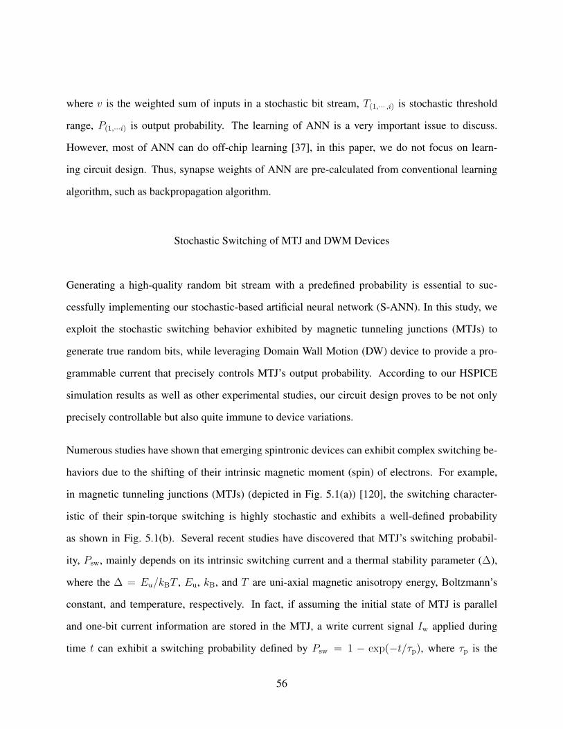
where v is the weighted sum of inputs in a stochastic bit stream, T(1,··· ,i) is stochastic threshold
range, P(1,···i) is output probability. The learning of ANN is a very important issue to discuss.
However, most of ANN can do off-chip learning [37], in this paper, we do not focus on learn-
ing circuit design. Thus, synapse weights of ANN are pre-calculated from conventional learning
algorithm, such as backpropagation algorithm.
Stochastic Switching of MTJ and DWM Devices
Generating a high-quality random bit stream with a predefined probability is essential to suc-
cessfully implementing our stochastic-based artificial neural network (S-ANN). In this study, we
exploit the stochastic switching behavior exhibited by magnetic tunneling junctions (MTJs) to
generate true random bits, while leveraging Domain Wall Motion (DW) device to provide a pro-
grammable current that precisely controls MTJ’s output probability. According to our HSPICE
simulation results as well as other experimental studies, our circuit design proves to be not only
precisely controllable but also quite immune to device variations.
Numerous studies have shown that emerging spintronic devices can exhibit complex switching be-
haviors due to the shifting of their intrinsic magnetic moment (spin) of electrons. For example,
in magnetic tunneling junctions (MTJs) (depicted in Fig. 5.1(a)) [120], the switching character-
istic of their spin-torque switching is highly stochastic and exhibits a well-defined probability
as shown in Fig. 5.1(b). Several recent studies have discovered that MTJ’s switching probabil-
ity, Psw, mainly depends on its intrinsic switching current and a thermal stability parameter (∆),
where the ∆ = Eu/kBT , Eu, kB, and T are uni-axial magnetic anisotropy energy, Boltzmann’s
constant, and temperature, respectively. In fact, if assuming the initial state of MTJ is parallel
and one-bit current information are stored in the MTJ, a write current signal Iw applied during
time t can exhibit a switching probability defined by Psw = 1 − exp(−t/τp), where τp is the
56

switching time constant. According to the paper [113], its switching probability Psw can be con-
trolled by changing the applied pulse width and amplitude [46] and can be concisely formulated
as Psw(I) = 1− exp(− tτp
exp(−∆(1− I/Ic0))), where Ic0 is the critical switching current at 0 K.
Therefore, by controlling the critical current Ic and the duration of applied pulse current τp, one
can accurately predict the switching probability of a given MTJ device. In 5.1(c), we have plotted
some of our experimental and analytical results of switching probability vs. the pulse duration for
different voltages [106, 83].
I
D1 D2
T1 T2
T30.0 ns
0.1 ns
0.2 ns
0.3 ns
0.4 ns
0.5 ns
(a) (b)
Figure 4.5: (a) Spin-torque-transfer DW device structure (b) Micro-magnetic simulation of freelayer DW motion when injected current density is 1.5× 10¹³A/m2
To generate random bits with different probabilities, we have to provide a specific writing current
to the MTJ device. In this work, we control the magnitude of writing current by using a fix voltage
supply across a DWM device that acts a programmable resistance. A DWM device typically has
two terminals, whose resistance can be precisely controlled by injecting a current density that
moves its domain wall. In Fig. 4.5(a), the DW device has two terminals (T1, T2) separated by
the non-magnetic region called domain wall (DW) D2 [37]. The thin nano-magnetic domain with
size of 3× 20× 100 nm3 is connecting two anti-parallel nano-magnetic domain terminals T1 and
T2. Usually, the terminal T1 receives an input signal, whereas, terminal T2 is grounded. Since
the domain wall moves in the direction of spin-polarized electrons, spin polarity of domain D1 is
57

written parallel to T1. Therefore, the domain wall can move through magnetic nano strip by the
current injection, which leads to switching of the spin polarity in DW strip at a specific location [37,
43, 38]. In Fig. 4.5(a), the area between D1 and D2 is indicating domain wall area and moving to
right by spin-polarized electron from T1. The moving of domain wall is affected by the magnitude,
direction, and duration of an injection current. Fig. 4.5(b) presents the simulation results of a
typical DWM device with the widely used mumax3 software. For the same time duration, the
magnitude of the injected current will determine the moving velocity of the domain wall, which
in turn changes the resistance across this DWM device. In Fig. 4.5(b), the position of this domain
wall position at different time is simulated, where 0.5 ns injected current with magnitude 1.5 ×
1013A/m2 is applied to terminal T1. The device parameters adopted in this simulation are shown in
Table 4.1: Domain wall device parameters.
Parameter Name Valueα Damping coefficient 0.02
Ku Uniaxial anisotropy constant 5.9× 10⁵J/m3
Ms Saturation magnetization 6× 10⁵A/mAex Exchange stiffness 1× 10¹¹J/mP Polarization 0.6
Table. 4.1. Our simulation results match very well with the results presented by Fukami [43] with a
critical current density∼ 6×10¹¹A/m2 and a moving velocity∼ 60m/s in a 20nm wide DW strip.
In our design, terminal T3 is used to read the position of the domain wall. The resistance model
of MTJ is based on supplying voltage, tunneling oxide thickness(tox), and angle of magnetization
between the free layer and pinned layer. The resistance model of a typical domain wall device is
described in [37, 40]. The equation is shown in as follows
R =A
B · x+ C(4.3)
where A = RAAP ·RAP ·RADW, B = (RAAP −RAP)RADW ·W , C = RAP ·RADW ·W ·L+
58

(RAAP · RAP − 0.5RAP · RADW − 0.5RAAP · RADW)W · LDW. In the equation on above, the
MTJ resistant is calculated by length of free layer (100nm), width of the free layer W, DW position
x (middle point), RAAP, RADW, and RAP are MTJ resistant area product for anti-parallel, DW,
parallel configuration, respectively. Thus, the output voltage can be computed as a rational function
of DW positions (0 < x < 100nm).
Stochastic-Based Synapse with STT Device
(a)
(b)
I
I
Input
Input
(c)
Figure 4.6: Circuit design of random bit stream generation. (a) Configuration mode. (b) Operationmode. Devices in gray area are active for each mode. Red curves depict signal directions. (c)HSPICE simulation of MTJ stochastic switching in 3 different devices which are programmedwith different probability values.
Fig. 4.6 presents our design of a reconfigurable random sample generator with one MTJ device and
one DWM device. Our key idea is to exploit the stochastic switching behavior of an MTJ device at
different input currents under a fixed pulse duration. Compared with the conventional LFSR-based
random number generation, such an MTJ-based methodology can provide not only true random-
ness but also ultra-fast generation speed. In its configuration mode (Fig. 4.6(a)), depending on
the precomputed stochastic weights, the domain wall device is configured with its resistance set
59

in order to produce the required writing current to MTJ. Paper [21] also shows the possibility to
mimic delay of generating random bit streams. With its proposed conditional perturbation scheme,
our random number generator can produce a bit rate 2.7 times faster and consume switch energy 6
times lower than conventional MTJ-based random number generator method. To evaluate this cir-
cuit design, we have performed detailed mixed-mode HSPICE circuit simulations using the model
of MTJ devices in Cadence from [117]. All specific device parameters are shown in Table. 4.2. To
illustrate, in Fig. 4.6(c), we plotted the HSPICE simulation results of three different MTJ devices
with different programmed probability, which illustrates that MTJ devices can indeed generate
specify stochastic bit streams with different programming currents and that the outputs of different
MTJ devices with the same programming current are fully independent.
The probability of spin-torque switching model Psw(I) according to the current I is given by
Psw(I) = 1− exp(−τp exp(−∆(1− I/Ic0))), (4.4)
where I is applied current, τp is the pulse width normalized by the attempt time. However, Chan-
thbouala [17] et. al. have shown that, for a given DWM device, a vertical current may also shift
its DW position with a current density higher than its critical value. This phenomenon is called the
effect of out-of-plane or out-of-field, which should be avoided in a reliable circuit design. In [37],
through extensive micro-magnetic simulations with various vertical current injections, the authors
have shown that the vertical critical density required to de-pin a DW is around 5 × 10¹⁰A/m2.
Therefore, the maximum vertical sensing current is 30µA without causing the effect of out-of-
plane [17]. In our proposed design, the maximum vertical sensing current of our DW devices can
only produce a very small writing current to MTJ device, while the required writing current for
switching probability changing from 0 to 1 is around 190µA ∼ 257µA. To overcome this issue,
we employ a Negative-Positive-Negative (NPN) transistor to amplify a small input current into
60

a larger output current. As shown in Fig. 4.6, our results have shown that an input small sensing
current to NPN base terminal can be effectively boosted into a larger current at Emitter with a 0.5V
supplied voltage Vcc at Collector.
(a) (b)
Figure 4.7: (a) Simulation of NPN transistor with different supplied voltages Vcc, where the in-put current is generated from a DW sensing current and amplified through a NPN transistor (b)Simulation of a NPN transistor with different parameters β
.
As shown in Fig. 4.7(a), we have simulated an NPN transistor at different supplied voltages Vcc
with SPICE software tools. Specifically, we have chosen an 2N3019 silicon NPN transistor from
Semicoa semiconductors with its Collector-Emitter Voltage VCEO, Collector-Base Voltage VCBO,
and Emitter-Base Voltage VEBO to be 80V, 140V, and 7V, respectively. In Fig. 4.7 (b), the SPICE
simulation of a NPN transistor with different β values has been performed, where the parameter
β of most standard NPN transistors can be found in their manufactures data sheets but generally
range between 50 and 200. In its operation mode (Fig. 4.6(b)), depending on the applied logic
input, a “0” or “1” value is first written into the right MTJ. Subsequently, a stochastic reading
current will be used to perform a read operation on this MTJ device. The logic output values
of this MTJ device, i.e., the random samples, are completely determined by both the logic value
stored and its probability of successful reading, which in turn is determined by the magnitude of
its reading current I . Note that, by controlling the reading current I and fixing Ic0, ∆, and τp, we
can match a specific weight with a predefined probability value. Finally, the magnitude of reading
61

current I is determined by the reading voltage that is controlled by the resistance of the domain
wall device. Fig. 4.8(a) and (b) show its corresponding DW device position and its injected current
density for generating different probabilities.
(a) (b)
Figure 4.8: (a) The equivalent DW position used for generating corresponding probability throughMTJ device (b) The equivalent writing current used to inject into DW device for generating corre-sponding probability through MTJ device
0 1 110
(a)
0 1 0 1 0
1 1 0 1 0 1 01 1 0
1 1 0 0 1 000 0
(b)
(c)
0
Input
MTJ write
Weighted output
Figure 4.9: Depiction of weighting operation of a synapse.
To perform the weighting operations towards inputs, we propose a new stochastic-based weighting
circuit that is functionality equivalent to a real number multiplier. We assume all inputs are encoded
with random bit streams that carry information. Fig. 4.9 shows the basic idea of proposed synapse
62

0 100 200 300 400 500 600 700 8000
0.5
1
1.5
Number of samples(a)
Vo
ltag
e (V
)
0 100 200 300 400 500 600 700 8000
50
100
Number of samples(b)
Cu
rren
t (µ
A)
0 100 200 300 400 500 600 700 8000
50
100
Number of samples(c)
Cu
rren
t (µ
A)
Figure 4.10: Simulation results of proposed new stochastic weighted topology (a). Input bit streamof stochastic neuron (b). MTJ bit stream according to writing current (c) Output bit stream
to implement weighted input.
As an example, in Fig. 4.9(a), the input bit stream has 0.5 probability is shown. The bit stream
with 0.6 probability in Fig. 4.9(b) is generated by an MTJ device with constant writing current.
The weighted output is obtained by a joint event, that is the input is 1 while MTJ device is 1.
To implement topology in our proposed architecture, we connect input bit stream to the switch
transistor with sensing voltage Vc to DW device. The NMOS transistor turns ON at time of in-
put is 1 and leads to writing current pass through MTJ device. The supplied writing current has
a unique probability to switch MTJ device. Thus, the output bit stream is generated depends on
input probability and MTJ switching probability. This joint event can be realized by multiplica-
tion between two probability in the stochastic domain. Therefore, the weighted input is obtained
through two probability multiplication. In Fig. 4.10, the input bit stream shown in Fig. 4.10(a) is
63
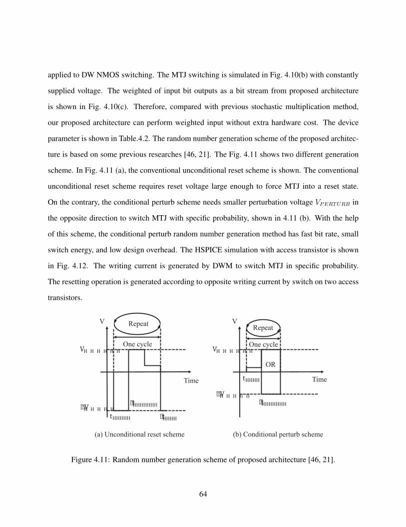
applied to DW NMOS switching. The MTJ switching is simulated in Fig. 4.10(b) with constantly
supplied voltage. The weighted of input bit outputs as a bit stream from proposed architecture
is shown in Fig. 4.10(c). Therefore, compared with previous stochastic multiplication method,
our proposed architecture can perform weighted input without extra hardware cost. The device
parameter is shown in Table.4.2. The random number generation scheme of the proposed architec-
ture is based on some previous researches [46, 21]. The Fig. 4.11 shows two different generation
scheme. In Fig. 4.11 (a), the conventional unconditional reset scheme is shown. The conventional
unconditional reset scheme requires reset voltage large enough to force MTJ into a reset state.
On the contrary, the conditional perturb scheme needs smaller perturbation voltage VPERTURB in
the opposite direction to switch MTJ with specific probability, shown in 4.11 (b). With the help
of this scheme, the conditional perturb random number generation method has fast bit rate, small
switch energy, and low design overhead. The HSPICE simulation with access transistor is shown
in Fig. 4.12. The writing current is generated by DWM to switch MTJ in specific probability.
The resetting operation is generated according to opposite writing current by switch on two access
transistors.
Time
V Repeat
One cycle
Time
VRepeat
One cycle
OR
(a) Unconditional reset scheme (b) Conditional perturb scheme
Figure 4.11: Random number generation scheme of proposed architecture [46, 21].
64

0 10 20 30 40 50 60 70 80 900
0.5
Time (ns)
VS
1 (
mV
)
0 10 20 30 40 50 60 70 80 900
0.5
Time (ns)
VS
2 (
mV
)
0 10 20 30 40 50 60 70 80 90−1
−0.5
0
0.5
Time (ns)
I MT
J (µ
A)
0 10 20 30 40 50 60 70 80 90−1
0
1
Mx
Time (ns)
0 10 20 30 40 50 60 70 80 90−1
0
1
My
Time (ns)
0 10 20 30 40 50 60 70 80 90−1
0
1
Mz
Time (ns)
Figure 4.12: HSPICE simulation of proposed architecture with writing and resetting operation.
Table 4.2: MTJ device parameter.
Parameter Name ValueId0 - 0.1nAn - 2
Ic0s Critical current 50µARP Resistance (P) 1kΩ
RAP Resistance (AP) 2kΩE/kBT - 60trelax Relaxation time 50ps
t Attempt time 1ns
65

Stochastic-based Soft-limiting Neuron
x
y
0 th1 th2
H
0
(a) (b)
Figure 4.13: (a). The transfer function of ANN neuron (b). Architecture of proposed stochastic-based linear transfer function neuron.
The key computing elements in an ANN are neurons interconnected with synapses, each of which
transforms its input signal through a neural transfer function. In this section, we describe our pro-
posed circuit implementation of a soft-limiting neuron with multiple Domain Wall Motion (DWM)
devices. Conceptually, the functionality of a neuron consists of two parts: summing weighted input
signals and applying a transfer function. Following our stochastic-based design principle, i.e., all
neural signals are encoded as a random bit stream, the summation of all weighted inputs can be
readily implemented through Kirchhoff’s Voltage Law by aggregating all input random bits streams
directly. Particularly, we connect in parallel all input current sources Ii to the current load (DWM
devices). To accurately implement a soft-limiting piecewise-linear transfer function in Fig. 5.8(a),
we developed a multiple-phase pumping circuit depicted in Fig. 5.8(a). Specifically, the general
form of a neuron transfer function can be defined with three key parameters: th1, th2, and H . th1
and th2 denote the starting point and ending point of linear neural signal transformation, while
∆ = Hth1−th2
denote the slope of signal change.
66

We now describe the working mechanism of our multiple-phase pumping circuit. As the input
signal increases, the domain wall of DW1 becomes more likely to move. When the first time Vin
exceeds the threshold voltage of DW1, its domain wall starts to move, which subsequently starts
to drive its next DW stage. As Vin further increases, more DWM devices will move their domain
wall. Finally, the last DWn will start to move its domain wall. Overall, it should be clear that DW1
and DWn determine th1 and th2, respectively, while the middle stages will determine ∆ = Hth1−th2
.
0 10 200
50
Time(ns)
Curr
ent
(µA
)
P=0.3
0 10 200
50
Time(ns)
Curr
ent
(µA
)
P=0.3
0 10 200
50
Time(ns)
Curr
ent
(µA
)
P=0.6
0 10 200
50
Time(ns)
Curr
ent
(µA
)
Sum
0 10 200
50
100
Time(ns)
DW
posi
tion (
nm
)
DW
Figure 4.14: SPICE simulation of DW1 device receiving sum of input current pulse. The 3 inputscurrent pulse with probability 0.3, 0.3, 0.6 is summed through connecting in parallel. Differentmagnitude of current pulse leads to different DW speed.
DW1 depicted in Fig. 5.8 receives the sum of weighted input currents, with the domain wall po-
67

sition of DW1 depending on the magnitude and the number of the high current pulse. Fig. 4.14
presents the SPICE simulation results of a DW1 device receiving the sum of input current pulses.
To further illustrate the effectiveness of our multiple-stage pumping circuits in 5.8(b), we first sim-
ulate a two-layer stochastic-based soft-limiting linear neuron depicted in Fig. 5.9. In Fig. 5.9(a),
the relationship between the positions of DW1 and DWn is presented. With more current pulses
inject into DW1, the position of DW1 is shifting and decreasing this DW device’s vertical resis-
tance. As mentioned in the previous section, in order to keep good sensing margins, the maximum
vertical sensing current should be 30µA. Therefore, the injection current is below the critical cur-
rent of DW2 device and shifting DW2 device, when the moving position of DW1 is small and kept
in high resistance range. Therefore, the lower threshold th1 is implemented by the critical current
of DW1. On another side, th2 is obtained by the max sensing current and the length of DW device.
In Fig. 5.9(b), the corresponding voltage output of DW2 is shown. In our simulation, we examined
4 different magnitudes of writing current at DW1. Different magnitudes of writing current at DW1
lead to a variety of DW1 positions. The high magnitude of applied current leads to the high DW
speed, while a low magnitude of applied currents leads to the low DW speed. In our simulation,
we have considered 4 different magnitudes of writing currents at DW1 which is leading 13 to 5
positions of DW1. This number of DW positions has two impacts on our transfer function, the
number of outputs and its variation. For example, if DW1 has 13 positions, DW2 can output 13
different voltages. If DW1 has 5 positions, DW2 can output 5 different voltages. However, there
is a trade-off between the number of positions and variation. Since the DW device has a stochastic
switching probability, more DW positions may cause larger variations.
Furthermore, adding more DW layers can match with different slopes of transfer functions. In
Fig. 5.9(c), we present different transfer functions with different layer numbers L. The multi-stage
pumping architecture of our stochastic-based neuron can increase the DW velocity of the next
layer. For example, a 3-stage neuron consists of 3 DW device chained together.
68

(c)(b)(a)
Figure 4.15: (a) mumax3 simulation of DW1 position and corresponding DW2 position (b)mumax3 simulation of DW1 position and corresponding DW2 voltage output (c) mumax3 sim-ulation of transfer function with different DW layers.
Because each DW device reads its out through its vertical sensing current, the horizontal DW
resistance is fixed by device width and length. In our simulation, we chose the horizontal DW
resistance Rw to be 294.5Ω [43]. Therefore, the final DW layer can receive a higher-magnitude
current from the second layer DW device. Thus, with the DW layer number L increasing, the slope
of its transfer function is increased.
Hardware Implementation of S-ANN
Fig. 4.16 depicts the overall circuit architecture of a typical S-ANN. It consists input, output, and
hidden layers, each of which is implemented with MTJ and DWM devices that operate according
to our stochastic-based computing principle. At its input layer, the proposed spin-transfer-torque
random number generator generates an input bit stream with a unique probability. For a fully
connected neural network, an input xi connects to all nodes in the hidden layer consisting of
multiple synapses and neurons in parallel. Specifically, let xi denote the input bit stream at the ith
input at a jth node.
69

Output
I
Input
. . .. . .
. . .
Output
. . .
. . .
Input Layer Output LayerHidden Layer
Figure 4.16: Overall Architecture of S-ANN.
When xi arrives, a corresponding synapse will receive this input bit stream and generate another bit
stream according to the input and synapse weight probability. For example, by giving the input bit
stream xi with 0.5 probability and programmed weight resistance corresponding to 0.6 weighted
probability, thus, the weighted output bit stream has 0.3 probability. The Fig. 4.16 shows the archi-
tecture of proposed synapse, which is also described in the previous section. The input bit stream is
applied to NMOS switch to control writing MTJ. The output bit stream is generating with probabil-
ity of Pxi ·PWi,j, where Pxi and PWi,j
denote the probability of input bit stream and the probability
of synapse weight, respectively. Subsequently, all input bit streams are summed through Kirch-
hoff’s Voltage Law (KVL) and then fed to the DWM-based soft-limiting transfer function, which
converts its input information into a specific voltage at output layer. One interesting observation of
our S-ANN is that, while in a real biological model, the inter-neuron communication runs through
axons, in our proposed S-ANN architecture, neurons transmit random bit streams between them,
which is quite similar to spike neural network.
70
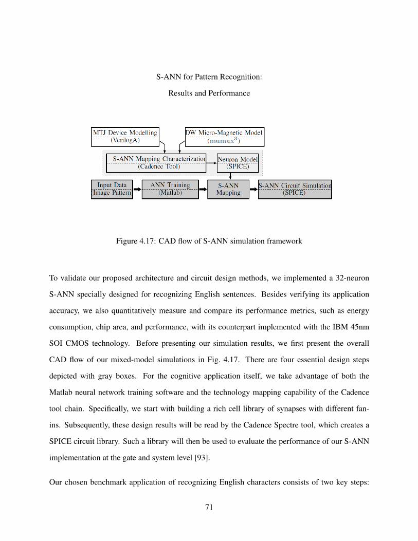
S-ANN for Pattern Recognition:
Results and Performance
Figure 4.17: CAD flow of S-ANN simulation framework
To validate our proposed architecture and circuit design methods, we implemented a 32-neuron
S-ANN specially designed for recognizing English sentences. Besides verifying its application
accuracy, we also quantitatively measure and compare its performance metrics, such as energy
consumption, chip area, and performance, with its counterpart implemented with the IBM 45nm
SOI CMOS technology. Before presenting our simulation results, we first present the overall
CAD flow of our mixed-model simulations in Fig. 4.17. There are four essential design steps
depicted with gray boxes. For the cognitive application itself, we take advantage of both the
Matlab neural network training software and the technology mapping capability of the Cadence
tool chain. Specifically, we start with building a rich cell library of synapses with different fan-
ins. Subsequently, these design results will be read by the Cadence Spectre tool, which creates a
SPICE circuit library. Such a library will then be used to evaluate the performance of our S-ANN
implementation at the gate and system level [93].
Our chosen benchmark application of recognizing English characters consists of two key steps:
71

edge extraction and pattern matching. The topology, synapse weights, and neural transfer functions
of our S-ANN are designed and trained off-line with standard software. In addition, edge extraction
is also pre-calculated. A training set of 1000 images, each of which has 108 feature vectors, is
used to pre-calculate and train our feed-forward S-ANN that contains one hidden layer and one
output layer depicted in Fig. 4.18 (a). After the training process, predetermined input voltages are
applied to each stochastic-based synapse (discussed in Section 4) of this S-CNN. Various weighted
stochastic bit streams are then generated according to these input voltages to accomplish the task
of probabilistically computing weighted sums. Next, all resulting combined random bit streams
are fed into the stochastic-based soft-limiting neurons discussed in Section 4.
(a) (b) (c)
Figure 4.18: (a) Architecture of a feed-forward ANN for hand written recognition tasks (b) Outputneuron voltage distribution, output neuron O1 has higher voltage than other output neurons wheninput pattern is A. (c) Normalized input pattern and output neuron, each block (i, j) indicates jth
winner output neuron of ith input pattern.
Table 4.3: Number of neurons with different transfer functions
Transfer Function Hard-limiting Soft-limitingStep Sigmoid STT-SNN [37] Proposed
# of hidden neuron 24 4 5 8# of output neuron 26 26 26 26
Our simulation results are shown in Fig. 4.18 (b) and (c). In Fig. 4.18(b), the output voltage
indicates the output neuron probability obtained by a DWM device. When the input character is
“A”, the output neuron O1 has a higher voltage than others, therefore indicating output neuron O1
72

to be the winner. Fig. 4.18(c) presents the quality of results achieved by our S-CNN. Each block
of this figure indicates how active output class jth is when an input target class belongs to the ith
alphabet. Our Spice simulations have also suggested that the voltage difference of a winner neuron
and other output neurons can be adjusted according to DWM device reading voltage supplies.
Table 4.3 lists a different number of neurons in MATLAB neural networking training software by
using different transfer functions with the same benchmark and recognition accuracy. It clearly
shows that a hard-limiting ANN requires more hidden neurons than other soft-limiting transfer
function methods. This is because soft-limiting transfer functions have much more modelling
capability with continuous outputs when compared with hard-limiting ones. One strength of our S-
ANN architecture is its capability of flexibly and accurately implementing any given soft-limiting
neural transfer function. More details can be found in Section 4.
(a) (b)
Figure 4.19: (a) Energy for different single neuron implementations. (b) Hidden layer area basedon different transfer functions.
Both energy consumption and chip area are measured for our stochastic-based ANN. The energy
consumption of an S-ANN can be divided into three parts: programming, sensing, and resetting.
For programming part, lateral currents of 30µA on average are injected into DWM devices for
different weights with resistances around 200Ω. Therefore,each synapse’s programming energy
is calculated to be approximately 0.4fJ with clock cycle period being 1ns. For the sensing part,
73

the multiple MTJ reading and writing process are accounted. Our measured energy consumption
for sensing matches well with the reported results of [21] for a MTJ-based true random number
generator. Specifically, for generating 8 bits random numbers, the total energy consumption of
sensing part measures to be about 24fJ. For the resetting part, roughly 0.75fJ in energy is consumed
using a 50µA current, We now compare our S-ANN circuit implementation with other recent
analog, digital, and emerging device neurons in [97, 94, 37, 90] in terms of energy consumption.
In Fig 4.19, the minimal energy consumption design is from Sharad [97]. Although this step
transfer function design has higher hidden neuron area than soft-limiting, each neuron employs
new techniques, such as spin-orbit coupling to increase DW speed, small sensing current, leading
to a very small energy consumption. The soft-limiting spin torque ANN is proposed by Fan et.
al. [37]. The energy saving benefit of the soft-limiting transfer function and low power spin torque
device are both described in [37]. As depicted in 4.19, our proposed S-ANN design consumes
slightly more energy than the two designs aforementioned, because stochastic computation needs
multiple clock cycles to compute. However, comparing with analog and digital implementation
method, our S-ANN implementation has 1.5 orders of magnitudes smaller energy consumption.
As shown in Fig. 4.19(b), our proposed soft-limiting ANN also leads to a reduced number of hid-
den neurons. Moreover, our stochastic-based soft-limiting ANN is very compact due to 3D layout.
Because DWM devices and MTJ devices are in nanometer scale, when taking into consideration
of their 3D structures, their impacts on the total chip area are quite minor when compared with
MOSFET transistors [61]. Specifically, numerous previous synapse designs based on memristor
crossbar consume about 150µm2 area with the size of each memristor is around 4F 2 [114]. In fact,
the distance of two memristors in the crossbar needs to be about 300nm [60]. Similarly, in order
to avoid coupling, the distance between two MTJ devices is quite similar with memristors [65],
requiring approximately 300nm. Our benchmark application needs 64 input nodes. Therefore, a
full-connected neural network, each node in its hidden layer requires 64 synapses and one neuron,
74

with total 8 nodes, while its output layer contains 26 nodes, each of which contains 5 synapses and
1 neuron. Although our piecewise linear soft-limiting transfer function does need more synapses
and neurons than sigmoid soft-limiting transfer functions, our proposed S-ANN still leads to ap-
proximately 2x lower hidden layer area than the hard-limiting step functions.
(a) (b) (c)
Figure 4.20: (a) Input hand written image of A-Z alphabets (b) Input hand written image of ”AD-JUSTMENT IS LIFE” (c) Input hand written image of ”LIFE IS TOO COMPLICATED IN THEMORNING” (d) The comparison of number of pattern recognitions with two different methods forinput image from (a) under increasing device variations (e) The comparison of number of patternrecognitions with two different methods for input image from (b) under increasing device varia-tions (f) The comparison of number of pattern recognitions with two different methods for inputimage from (c) under increasing device variations
Most existing studies on implementing neural networks with emerging device technologies follow
the conventional design methodology of digital or analog circuits for deterministic computing. As
such, the stochastic switching behavior and their susceptibility to noise of emerging devices have
posed significant design and implementation challenges. In contrast, our proposed stochastic-
based soft-limiting ANN are highly tolerant to device variations. Instead of combating with their
inherent stochastic switching behaviors, our S-CNN directly exploits them for efficient computing.
Fig. 4.20 compares the number of recognized patterns between a state-of-the-art STT-SNN [37]
and our S-ANN implemented with MTJ and DWM devices with increasing device variations and
different input images. Fig. 4.20(a)(b)(c) demonstrate the different input images for training and
detection, while Fig. 4.20 (d)(e)(f) compare the results of pattern recognitions given different in-
75

put images with 26, 16, 32 patterns, respectively. Not surprisingly, as shown in Fig. 4.20(d)(e)(f),
the number of recognized patterns consistently decrease with the increase of device variations.
However, the STT-SNN implementation suffers from a clearly more precipitous drop in its quality
of results. This is likely because the device variation of memristor conductance has a significant
negative impact on the performance of deterministic synapses. On the other hand, the perfor-
mance degradation of our S-ANN implementation is much slower largely due to the robustness
of its stochastic design, which comes from two major sources: 1) random bit generation through
stochastic switching is much more reliable for MTJ devices, and 2) when information is encoded
with random bit streams, complicated operations can be converted into much simpler operations
that are typically not only cheaper to implement but also much more error-resilient.
In the following, we provide an intuitive explanation of the robustness of our proposed S-ANN
implementation. In our S-ANN network, each signal X is represented as a stochastic bit stream
with its expected value E[X] = pX . As in a conventional deterministic-based neural network, the
value of signal X in our S-ANN will also be distorted with errors manifested by flip errors of its
random bit stream. Let e denote the bit error vector with an expected value pe, the stochastic signal
X thus becomes X∗ = X⊕
e. Mathematically, the expected value of the signal X with its bit
flipping errors can be defined as
pX∗ = E[X] = pX + pe(1− 2px) (4.5)
With the standard definition of mean square error (MSE), the difference between the estimated
value pX∗ and the exact value pX can be written as
EX∗ = E[(pX∗ − pX)2] (4.6)
In our S-ANN, we assume the estimated value pX∗ to be the average of n independent random
76

samples of X∗, which is equal to pX∗ = 1/n∑n
i=1 = X∗i . Therefore, the expected value of X∗
can be written asEX∗ = E[(p2
X∗ − p2X − 2pX pX∗)]
= (pX∗ − pX)2 +pX∗(1− pX∗)
n.
(4.7)
Combing Equation (6) and (8) leads to
EX∗ = p2e(1− 2pX)2 +
1
n[pX(1− pX)
+pe(1− pe(1− 4pX(1− pX)))]
(4.8)
This clearly shows that the MSE error of X depends on both bit stream probability pX and bit flip
error rate pe. With the increasing of a bit stream size n, EX∗ monotonically decreases. Given a
sufficiently large n, EX∗ quickly converges. Also, Equation (9) also reveals that the bit stream
probability of pX = 1/2 has better error resilience. Guided with the above analysis, we have
conducted extensive Monte Carlo simulations with 32 as the bit switch.
0 0.05 0.1 0.15 0.2 0.250.005
0.01
0.015
0.02
Bit Flip Error Rate
Mea
n−
Sq
uar
e E
rro
r
Analytical
Simulation
0 0.2 0.4 0.6 0.8 10
0.005
0.01
0.015
Probability of Input px
Mea
n−
Sq
uar
e E
rro
r
Analytical
Simulation
Figure 4.21: (a) The MSE simulation of stochastic bit stream with increasing of bit flip error rateboth in analytical and simulation method. (b) The MSE simulation of stochastic bit stream withdifferent probability both in analytical and simulation method [19].
Fig. 4.21 presents our simulation results and clearly shows that our stochastic method possesses
inherent error resilience. As such, device or circuit errors have much less effect on the expected
77

value of a stochastic bit stream. Specifically, even a portion of a stochastic bit stream (n bits in
size) are flipped, their negative effect to the overall expected value will be reduced by n times.
More importantly, such an error will be significantly diminished as n increases. Furthermore, bit
flipping in a digital circuit tend to be symmetrical, i.e., equal numbers of 0− to−1s or 1− to−0s.
As a result, a large portion of bit flipping within a given random bit stream will naturally cancel
out, thus posing negligible error on the overall X value [19].
Analytical Error Study
200 210 220 230 240 2500
0.2
0.4
0.6
0.8
1
Switching current(uA)
Sw
itch
ing
pro
ba
bili
ty
Simulated result
Theoretical result
Figure 4.22: Simulation of theoreticaland simulated results.
0.020.02
0.02
0.020.02
0.02
0.04
0.0
40.04
0.0
6
0.0
6
0.06
0.0
8
0.0
8
0.1
0.1
0.1
2
0.1
20.1
4
L
Pro
ba
bili
ty
0 100 200 300 400 5000
0.2
0.4
0.6
0.8
1
Figure 4.23: Random bit stream errorwith different bit length.
To further validate our proposed S-ANN design methodology, we now quantitatively consider
various error components in our proposed architecture. MTJ Random Number Generation Error
( em) forms the first error component of our stochastic synapse circuit. Mitigating MTJ device
variations have been the main focus of many kinds of research. Fortunately, our method utilizes
MTJ’s probabilistic switching behavior to build up the stochastic computing scheme, therefore
quite insensitive to its device variations. As discussed in Section 4, a MTJ’s switching probability
Psw mainly depends on critical current Ic0 and thermal stability parameter σ, therefore the variation
of these two parameters need to be considered. Because the switching probability of a MTJ can be
78

defined as Psw(I) = 1− exp(−τp exp(−∆(1− I/Ic0))), the l2 norm least square error of a given
switching probability can be written as as em =∫ n
0|Psw − Pmeasure|2dIn, where the Pmeasure is the
measured probability of switching. Using the above error model to analyze the impact of variation
of electrical parameter on MTJ device, as shown in Fig. 4.22, the matching between the model
simulation and theoretical results is very high. The paper of [20] proposed a similar architecture
of true random number generator fabricated on the chip. The results experimentally demonstrate
true random number generator based on the stochastic switching behavior of MTJ device. The true
random number generator based on the stochastic switching behavior of MTJ device enhance the
reliability, speed and power consumption to generate a true bit stream.
The random bit fluctuation error (er) is due to the bit flips in a stream. In this paper, since the
number of ones in the bit stream will be used to compute the value of stochastic ANN, the error of
bit fluctuations will affect the stochastic ANN. The bit stream Bi with i = 1, 2, · · · , n has L length
bit stream. The number of ones in a bit stream is converted to a deterministic value T through the
integrated circuit. Because T = 1L
∑Li=0Bi, the expected value is Te. However, due to the random
fluctuation error, the exact output T value is different from the excepted value Te. The random
fluctuation er can therefore be written as er = |T − Te| ≈√
Te(1−Te)L
. In this paper, the expected
value Te is calculated from the measurements of the output bit stream. The relationship between
different probability and different length of random samples is shown in Fig. 4.23.
Finally, we consider the error due to DW integration. The DW integration determines the number
of ones in a given bit stream. According to the experimental work reported in [45], the reliability
of a typical domain wall device is excellent. For example, a Co/Ni wire can achieve a 10-year
retention time at 150 degrees and 1 × 10¹⁴ times write. In addition, the experiments in [45] have
also shown that the domain wall velocity and critical current are not sensitive to external magnetic
field or temperature.
79

Conclusion
Emerging device technologies excel in their energy efficiency and performance when compared
with the conventional CMOS technology in performing cognitive computing tasks. However, they
are known to suffer from large device variations and mediocre device reliability. This study is
our attempt of investigating innovative circuit designs and operating principles to directly exploit
emerging devices’ stochastic switching behaviors for implementing robust and stochastic-based
artificial neural network (S-ANN). In the future, we plan to continue exploring other neuromor-
phic computing architectures by leveraging unique electrical characteristics of emerging device
technologies.
80

CHAPTER 5: SPIN-TRANSFER-TORQUE-DRIVEN AND
NEURON-BASED FPGA ARCHITECTURE WITH EMERGING
DEVICES
Introduction
bbbaaa
Figure 5.1: (a) Cross-section of a MTJ-CMOS hybrid chip. (b) Monolithically stacked 3D-FPGA [73].
Emerging spintronic devices, such as spin-valves and domain-wall magnets (DWM), have rekin-
dled significant research interests in novel circuit and architecture design methodologies [98, 58].
Sharply deviating from CMOS device technology, spintronic devices use electron spin, instead
of charge, as the medium of information processing, therefore offering not only ultra-low critical
current (e.g., ≤ 100 µA at 65 nm), simple switching scheme, and non-volatile, but also many fas-
cinating probabilistic-related physical properties [107, 83]. In particular, as shown in Fig. 5.1(a),
Magnetic Tunnel Junctions (MTJ), the cornerstone of spintronic devices can be densely embedded
into CMOS logic circuits and fabricated with an extremely small footprint on top of the metal
layers and occupy almost “zero” chip area. Therefore, a hybrid MTJ-CMOS chip is considered by
many as a potentially powerful solution that brings non-volatility, instant on/off, and low standby
81

power to today’s IC technology.
Given the prominent role of FPGA in IC technology, it is natural to investigate how to exploit
emerging device technologies to improve the performance of modern FPGA, which, since its in-
ception, has always been at the forefront of IC technology innovation. In fact, studies on exploit-
ing emerging switching devices have recently surged. For example, newly developed memris-
tor devices have been investigated to replace SRAM as the storage of elements in CMOS-based
FPGA [18]. More recently, the nano crossbar architecture has been touted [24, 29]. as an even
more superior alternative to the conventional non-volatile phase-change memory due to its high
density and lower power consumption [81]. Another conceptually appealing approach to directly
applying MTJ-CMOS devices is to stack the programming overhead of an FPGA on top of the
logic blocks and interconnect layers that would be implemented in a state-of-the-art CMOS tech-
nology. This approach resembles the monolithically stacked 3D-FPGA architecture, as depicted
in Fig. 5.1(b), which achieves significant performance benefits [73, 72]. Despite achieving quite
encouraging performance improvements, the vast majority of these studies have focused on us-
ing spintronic devices as storage elements and configuration memory bits, therefore sharing the
same trait: no fundamental modification to the standard LUT-based FPGA architecture design and
circuit implementation.
Another motivation for studying how to leverage emerging device technologies to implement FP-
GAs is due to the fact that, although its technology, including hardware design and implementation,
logic synthesis, and technology mapping has been studied extensively over the past two decades,
progress within the last few years has slowed considerably in spite of significant advances in de-
vice technology. In fact, modern FPGA architecture strikingly resembles that of tens years ago.
Specifically, today’s FPGAs still consist of the same SRAM-based programmable logic and rout-
ing fabrics. We believe that both neuromorphic-based computing principle and emerging device
technology provide an important opportunity to innovate in FPGA technology. In fact, several re-
82

search works have been performed to design and implement bio-inspired computation systems in
hardware domain with emerging devices [35, 52, 102, 32, 16]. Among them, studies [102, 16] pro-
posed a realization of biologically inspired reconfigurable hardware through the memristor cross-
bar architecture. Although achieved quite promising results in robustness and power-delay product,
these designs all suffer from large writing energy of memristor and variation of crossbar architec-
ture. Most importantly, all these new FPGA architectures require significant modifications to the
current FPGA CAD design flow, which proves to a serious impediment to their wide adoption in
reconfigurable computing systems.
In this paper, we focus on developing a new Spin-transfer-torque-driven and Neuron-based FPGA
(SN-FPGA) architecture by leveraging the stochastic properties of emerging spintronic devices.
The SN-FPGA centers around the idea of implementing a flexible Multiple-Input-Multiple-Output
Logic Block (MIMO-LB) through constructing a light-weight artificial neural network with emerg-
ing devices. Our main objective is to develop an architecture that maximizes the application spec-
trum for both data-path and control-path applications without compromising performance and area
efficiency, while fully exploiting the performance benefits entailed by the emerging devices. In
addition, both the granularity and the input-output numbers of the new logic blocks can be dy-
namically configured on a per-mapping basis at configuration time. More specifically, our major
contributions include:
• We proposed a new curve-based method to reinterpret and redefine Boolean logic func-
tions, therefore can efficiently implement MIMO-LB without noticeable hardware usage
overheads through constructing an artificial neural network (ANN) with emerging spintronic
devices. Furthermore, based on some recent discoveries in neural computing [53], we math-
ematically proved that a feedforward neural network consisting of two hidden layers can
accurately realize a K-input-L-output LUT with only 2√
(L+ 2)2K hidden neurons. Note
83

that for a K-input-1-output LUT structure, our new Neuron-based LUT structure consumes
the same order-of-magnitude hardware as the conventional SRAM-based LUT. However,
our new LUT design consumes ≈ Ø(√L) times less hardware than the SRAM-based LUT
structure for multiple output LUT, which can be quite significant for large output values (L).
(See Section 5 for more detailed discussions). This property enables the hardware-efficient
implementation of large-fan-out logic blocks, which can potentially improve the overall per-
formance of a placed and routed circuit design.
• ANN circuit design with emerging devices, such as MTJ, is a centerpiece of this research. In
the past, due to its excessive hardware cost, ANN has not been considered as a viable circuit
solution for performing a Boolean logic function. in this paper, we developed various circuit
design techniques to natively exploits the physical behavior of the emerging spintronic de-
vices, therefore bypassing the excessive hardware overhead of Boolean-based methodology.
Specifically, we have developed new circuit implementation of synapse through heavy metal
layer associated with domain wall strips to imitate positive and negative synapse behavior.
Compared with memristor bridge synapse [59] and spintronic crossbar synapse [92], our
proposed all spin synapse is more efficient, because of less number device and high device
utilization. Furthermore, we proposed a novel multi-stage neuron architecture capable of
accurately realizing a diverse set of transfer functions. This flexibility proves to be essen-
tial in achieving much higher computing performance for different target applications, and
significantly simplifying its learning process.
The rest of our paper is organized as follows. In Section 5, we briefly overview the overall architec-
ture of the SN-FPGA. We then illustrate in Sections 5 and 5 how an MIMO-LB can be constructed
with spintronic devices. In particular, We review the newly discovered stochastic switching be-
havior of Magnetic Tunneling Junctions (MTJ), one of the most important emerging devices, and
discuss the circuit design of a typical MIMO-LB. Before presenting the performance comparison
84

results of three performance metrics (hardware usage, delay, and energy consumption) between
the SN-FPGA architecture and three other island-style baseline FPGAs in Section 5, we detail
each necessary module for logic synthesis, placement, and routing of a typical SN-FPGA device.
Finally in Section 5, we summarize our findings and comment on several open research problems
related to the SPGA architecture.
Architecture Overview of SN-FPGA
(a) (b)
Figure 5.2: (a) 2-D Island-style FPGA architecture. (b) SN-FPGA architecture with hybrid Spin-CMOS devices.
At a high level, the overall architecture of an SN-FPGA resembles that of the conventional well-
structured island style FPGA as shown in Fig. 5.2(a), in which an array of logic blocks (called Con-
figurable Logic Block, CLB, or Logic Array Block, LAB, depending on vendor) are surrounded by
pre-fabricated programmable routing channels and I/O pads. However, the SN-FPGA architecture
depicted in Fig. 5.2(b) differs from the existing norm in at least two aspects. First, in the traditional
CMOS-based FPGA technology, all configurable bits are implemented with memory devices such
85

as 6-T SRAM or anti-fuses. In the SN-FPGA, we do not use binary bits to “define” our target
logic function. Instead, we use the spin-based magnetization to configure the logic blocks. Sec-
ond, the functionality of the memory-based LUT hinges on the concept of K-map and is based on
the Boolean algebra. In a sharp contrast, our neuron-based LUT uses a new curve-based method
to reinterpret and redefine Boolean logic functions, therefore can efficiently implement a logic
block with a configurable number of logic inputs and outputs without negatively causing excessive
hardware overheads. Finally, given the 3D “nature” of the Spin-CMOS hybrid device technol-
ogy, we can redesign the interconnect architecture of the SN-FPGA. Specifically, the LB inputs
and outputs connect first to local segments These segments can then be programmable connected
to segments in neighboring routing blocks and/or to interconnect segments in a routing channels
via programmable buffers and muxes with buffered outputs. The interconnect segments can be
directly connected to form longer segments using programmable buffers without going through
routing blocks (we shall refer to such interconnects as bypass interconnects). In this paper, we opt
to focus on the first two design considerations due to space limitation.
MIMO-LUT: Idea and Methodology
The most common type of programmable logic element used in an FPGA is called a K-LUT,
i.e., a K-input one-output lookup table (LUT), capable of implementing any K-input one-output
Boolean function. Conceptually, a K-LUT can be looked as a hardware version of Karnaugh map
that encodes a complete truth table representing a K-input logic function. There are two strongly
correlated challenges of designing logically-efficient LUT structure.
• The first major challenge in FPGA architecture design is to determine the granularity of
logic blocks in an FPGA. All prominent FPGAs [1, 112] today have fixed and uniform logic
granularity for each logic block. From the architecture point of view, coarse-grain blocks
86

have much less stress on the placement and routing but often result in long internal logic
delays and under-utilization for designs in small size, whereas fine-grain logic blocks can
achieve shorter internal delay but often requires an excessive amount of routing resource in
order to successfully route a circuit. From the application point of view, data-path functions,
in particular arithmetic functions, often operate on coarser arguments than control-path logic
and are usually realized by fine-grain logic elements, while the implementation of control-
path logic mostly benefits from coarser granularity. A rather interesting question is whether
the logic blocks in an FPGA should be heterogeneous or homogeneous in size.
• The second challenge is to determine the optimal number of output bits. Numerous studies
have found that multiple-output logic block can significantly reduce the overall chip area
for FPGA synthesis. For example, researchers have developed a new re-synthesis algorithm
by considering multi-output functions and re-timing that incorporate recent improvements
to SAT-based Boolean matching. Their experimental results have shown that, with the in-
clusion of multi-output logic block, the total FPGA chip area can be reduced by up to 16%
when compared with the conventional single-output LUT-based FPGA architecture. Re-
cently, researchers have exploited the ability of PCM (Phase-Change Memory) to exist in
multiple intermediate states to store 2 bits per cell and develop a new Look Up Table (LUT)
architecture, which can emulate multi-output LUTs. Without even modifying the dominant
interconnect delay, they have found that their new multi-output logic block can achieve sig-
nificant improvements in logic density and performance with area improvements of over
40% for all LUT sizes and delay improvements of 7% to 13% on an average for LUTs of
size 10 to 6. All these studies have shown the significant performance benefits that can be
gained by enabling multiple-input-multiple-output logic blocks.
In the following, we take a quite different approach to reinterpreting the functionality of a LUT.
First, instead of treating it as a tabulated logic definition, we reformulate it as an algebraically
87

continuous function with discretely encoded inputs and outputs. We then proceed with discussing
how to implement or realize the aforementioned algebraic curve with a small-sized artificial neural
network (ANN). All these treatments will lay out a solid foundation for the new circuit implemen-
tation of a multiple-input-multiple-output LUT (MIMO-LUT) with emerging spintronic devices.
We have two objectives in designing our neuron-based LUT structure. First, our new LUT design
should be flexible in its granularity, namely, the number of inputs and number of outputs can be
readily configured to fit with the need of target circuits. Second, such flexibility of MIMO-LUTs
should not incur excessive hardware overheads. We now first present the key idea behind our
neuron-based MIMO-LUT and then discuss in detail how its circuit is implemented with emerging
MTJ devices.
Algebraically Reinterpreting LUT
To illustrate how we interpret the standard Boolean K-map in a different angle, we use a 4:2
encoder shown in Fig. 5.3(a) as an example, which can be represented as a truth-table listed in
Fig. 5.3(b). If we encode its binary input and output bits as decimal numbers, we obtain a single-
input-single-output function as in Fig. 5.3(c). Furthermore, such a functional one-to-one map-
ping can be plotted as a simple algebraic curve shown in Fig. 5.3(d). For example, as shown in
Fig. 5.3(a), when (D3, D2, D1, D0)=(0, 1, 0, 0), the output (Q1, Q0)=(1, 0), which can be com-
puted either by looking up the K-map in Fig. 5.3(b), or by evaluating the curve at the point (4, 2).
Conventionally, SRAM-based LUT design has been a dominating solution for modern FPGA de-
vices. However, such a conventional Look-Up Table (LUT), although logically universal, incurs
approximately O(2N ) of hardware cost for a N -input-1-output logic function due to the number of
required reconfiguration memory bits, which can be quite hardware-expensive. Moreover, SRAM-
based LUT makes implementing multiple-output also quite inefficient.
88

Figure 5.3: (a) Logic diagram of a 4:2 encoder. (b) Truth table. (c) Encoded inputs and outputs.(d) Logic curve interpretation.
In fact, the hardware cost increases almost linearly with the number of output bits. Note that
both representations in Fig. 5.3(a) and (b) are logically equivalent, albeit in totally different forms.
Moreover, any givenm-input and n-output logic function, with a properly chosen encoding scheme,
can be transformed into a well-defined algebraic curve. Therefore, we can recast the problem of
a logic circuit design into building hardware structure that performs functional evaluation by in-
terpolating algebraic curves. Unfortunately, although the artificial neural network is known to be
capable of approximating any form of complex algebraic function constant, directly performing
all these constituting operations are quite expensive in CMOS digital hardware. Fortunately, we
exploit the physical behavior of spin-torque-transfer devices, therefore completely bypassing the
aforementioned performance bottlenecks.
89

MIMO-LUT with Artificial Neural Network
ANN has been a subject of active research for decades due to the ability of human-like cognitive
computing and potential of the ultra-low power consumption [34, 32, 33]. The initial adaptive
systems of the ANN were motivated by the parallel processing capabilities of real brains, how-
ever, architectures of ANN only have little in common with real biological structures. Therefore,
a variety of ANN models has been studied and proposed [51]. The key computational units of
ANN are the neurons, which are connecting to each other and to external stimuli through pro-
grammable connections based on synapses [5, 37]. The basic operation of ANN is based weight
sum and non-linear transfer function which is expressed as Y = f(∑Wi · xi− T ), where Y is the
output of neuron or activation level, xi indicates ith input, Wi is corresponding synapse weight, T
denotes threshold and f is neuron transfer function. Fig. 4.1 shows multi-layer artificial neural net-
work with different transfer functions. Each neuron node in ANN consists of three mathematical
function blocks, weighted input, summation, and comparison.
Given our new algebraic interpretation of LUT, we propose to leverage the method of functional
approximation with artificial neural network in order to redesign the LUT circuitry. Our central
idea is to use an artificial neural network (ANN) to realize a well-defined multiple-input-multiple-
output (MIMO) function that in turn fulfills the functionality of an MIMO-LUT. To implement a
K-input-L-output LUT, we use a well-structured two-hidden-layer feedforward networks (TLFNs)
to learn all 2K distinct samples that define a K-input LUT. If using the same illustrative example
in Fig. 5.3, where K = 4 and L = 2, we propose to use an ANN with 4 input neurons and 2
output neurons as well as 16 hidden nodes to realize the functionality of a 4-input-2-output LUT.
Therefore, there are 24 training samples, each of which corresponds to a unique 4-bit input vector
for the target 4-bit encoder.
To validate the above approach, two important questions have to be answered. First, what should
90

be the topology of our proposed artificial neural network (ANN) and how many neurons are nec-
essary? Second, given sufficient training samples, what will the approximation error for a given
ANN? Fortunately, Huang [53] proposed a constructive method to prove that two hidden layer
feedforward with 2√
(L+ 2)2K hidden neurons can learn any 2K distinct samples with any ar-
bitrarily small error, where K and L are the number of input and output neurons, respectively.
Specifically, the authors of [53] have rigorously proved in a constructive way that TLFNs with
L1 =√
(L+ 2)2K + 2√
2K/(L+ 2) neurons and L2 = L√
2K/(L+ 2) neurons in the first and
second hidden layers, respectively, can learn 2K distinctive samples (xi,yi) with any arbitrarily
small error, where xi ∈ RK and yi ∈ RL, respectively.
0 2 4 6 8 100
5
Input Bits
Num
ber
of
SR
AM
Neu
ron n
odes
( X
1000)
S(O=1)
N(O=1)
S(O=2)
N(O=2)
S(O=3)
N(O=3)
S(O=4)
N(O=4)
S(O=5)
N(O=5)
O=1 O=2 O=3 O=4 O=50
400
SRAM
Neuron
Figure 5.4: Theoretical analysis of hardware usage of conventional (FPGA) method and neuralnetwork method.
To quantitatively compare the hardware usage of our proposed neuron-based LUT against the
conventional SRAM-based LUT, we showed in Fig. 5.4 the hardware usage of these two methods
for a given truth table.
In Fig. 5.4, we test hardware usage which is represented as a number of SRAM and hidden layer
nodes for traditional and neural network truth table implementations. For conventional method,
especially FPGA implementation, the number of SRAM cell to implement the given truth table
91

is increasing exponentially with input bit increasing and growing several times with output bit
increasing. On opposite side, neural network can learn the truth table with a small number of
hidden nodes. The increasing of input and output bit may increase the number of hidden nodes
slightly. While input bit number is small, especially less than 4, conventional method consumes
less number of SRAM cell compare with the number of hidden nodes of a neural network used to
learn given truth table. That is because neural network needs the minimum number of hidden nodes
which do not decrease with the number of input bit The subplot in Fig. 5.4 shows details of the
conventional method and neural network method at input bit is equal to 6. The trends of increasing
SRAM number of the conventional method is increasing drastically with output bit increasing.
On the contrary, hidden nodes neural network is increasing moderately. Therefore, at theoretical
analysis.
MIMO-LUT: Circuit Implementation
Spin-Transfer-Torque-based Artificial Neural Network
In ANN architecture, each neuron will receive multiple synaptic inputs and generates a correspond-
ing output that is delivered through axon. The basic operation of each neuron can be represented
by a simple weighted summation and consequently a transfer function. The main contribution of
this research is to construct a typical ANN using only spin torque devices. Specifically, our pro-
posed circuit architecture directly utilizes the physical characteristics of spin torque phenomenon
in order to achieve highly efficient neural operations. In particular, we use the programmable Spin
Orbit Torque (SOT) to emulate the functionality of a synapse. Our circuit is also operated in a cur-
rent mode, with the weighted summation current being generated through different SOT resistance
with the same applied voltage. One unique feature of our proposed circuit design is that it can
92

implement both positive and negative currents via positive and negative supplied voltage, which
effectively implements both positive and negative synaptic weights. In the literature of ANN, such
dual polarity of synaptic weights have been proven to be capable of significantly reducing the
overall training time of a given ANN.
In addition, we also proposed a multi-layer SOT neuron circuit that can implement a wide variety
of adjustable transfer functions that generate correct voltage outputs to the next stage via axon
NPN transistors. In particular, each of our proposed SOT neurons has two operation states, write
and read. During the write state, the synapse will generate unique input current to the specific
neuron, which then weighted-sum its applied voltage. During the read stage, this neuron transmits
its output current to the next stage through an axon NPN transistor. The current supplied by the
DW synapse is passing through the neuron. Since our proposed neuron circuit is constructed with
DWM devices, its neuron resistance is also considered to be in the path of the resultant synaptic
current. As such, the net synaptic current to this neuron is given by equation[92],
I =
∑iGiVi
1 + γ, (5.1)
where γ = Rneuron
∑iGi. Because the neuron resistanceRneuron is typically quite small compared
with the term 1∑iGi especially when γ 1, the voltage drop across our spin-based neuron struc-
tures can be safely neglected. Finally, the required supplied voltage on our proposed spin-based
synapses is determined by considering the necessary critical current for the domain wall displace-
ment between the two extreme edges of the free layer of our neuron. Therefore, there is a clear
trade-off between the slope of a linear transfer function and the net synaptic current. Fig. 5.5 de-
picts the overall circuit design of a typical SHE-based ANN according to our design. We clearly
marked three function blocks: synapses, neurons, and axons. In the following two sections, we
detail all circuit design techniques associated with our SHE-based neural synapses and neurons.
93

…
……
Axon
Neuron
Out
Synapses
Figure 5.5: Structure of proposed ANN. The synapse, neuron and axon are implemented throughall spin device.
All Spin Neural Synapse
The larger the slope linear transfer function needs more layer domain wall devices, which is also
causing larger γ. The higher input voltage may cause higher synaptic resistance and lower value
of γ.
In an ANN, synapse is the key computing element to perform weighted functions of incoming
neural signals, corresponding to the junctions between individual neurons in a biological system
that transfer neural signals from a transmitting neuron to a receiving neuron. For the SHE-based
synapse depicted in Fig. 5.6, we apply a constant applied voltage on its reading path. As shown
in Fig. 5.6(a), each of our proposed synapses consists of two DWM devices connected in series.
When two different supply voltages with constant magnitudes are applied, two reading currents in
opposite directions will be generated.
94

Write GND
(a) (b)
Figure 5.6: (a) Architecture of proposed synapse. (b) The equivalent circuit of proposed synapse.The two reading currents flowing through two opposite devices and weighted by device conduc-tance. The conductance is used to encode synaptic weight and program by DW position throughwriting current.
To understand their operations, we have also drawn the equivalent circuit of this reading operation
in Fig. 5.6(b). On each of these two devices, the fixed voltage applied at its read terminal and
GND terminal create a closed loop in the circuit, thus producing a reading current Is+ due to
the resistance of the DWM device caused by the state combination of a parallel, an anti-parallel
domain, and a free layer domain. In Fig. 5.6(b), an MTJ device shows its different states of
these domains with different arrows. Because the free layer domain has magnetization along its
horizontal axis, the heavy metal layer will add a constant resistance in its reading path. Fortunately,
the value of this resistance is negligible compared with the tunneling oxide resistance, thus has no
notable effect on the correct operation of our DWM-based synapse.
Analytically, the device conductance of a free layer can be defined as GP,max and GAP,max, where
the magnetization of a free layer is either parallel and anti-parallel to pinned layer. Therefore, the
95

total device conductance is given by,
GS+ = GP,max(x
L) +GAP,max(
1− xL
) +GDW , (5.2)
where GGW is the conductance of the domain wall region and L is length of whole device. If the
supplied voltage is a constant, the GGW , GP,max and GAP,max are all constants. From the above
equation, GS+ has a linear relationship with the domain wall position x. Thus, the device GS+
can be programmed by the DW position through a predetermined injected current at heavy metal.
The weighted current is generated by a constant voltage Vread and device conductance (encodes
as synaptic weights), IS+ = GS+ · VS+. In the reading operation, the hysteresis phenomenon,
the physical characteristics of DW depinning, can make the spintronic synapses read appropri-
ately without any domain wall motion. The Tunneling Magnetoresistance Ratio (TMR) value can
determine the ratio of synaptic weight which is encoded by its device conductance.
In [55], studies have shown that approximately 600% TMR values have been achieved through
lab fabrications, with . More than 1000% TMR values to be expected in about ten years [50].
In artificial neural networks (ANNs), negative weights are very important to describe an opposite
relationship between the two neurons. There are two common methods to implement negative
synaptic weight by emerging devices, memristor crossbar architecture [35] and memristor bridge
synapse [59]. However, for reconfigurable computing platform, these methods will cause a large
cost of power supplies and hardware. In this paper, we proposed a differential synapse imple-
mented with SHE-based domain wall motion (DWM) devices, which can readily generate either
positive or negative synaptic weights without an extra large cost of power supplies and hardware.
In Fig. 5.6(b), the combined reading current depends on the weighted readings from two opposite
device In a writing operation, the same writing current is injected in HM layers on two devices.
Thus, the positive and negative effective magnetic fields HSHE are created on up and down de-
96

vices, respectively. The effective magnetic fields HSHE working on DW region can be observed
as perpendicular to the plane of the magnetic. The same altitude and duration of injection current
make DW moving with the same velocity on both devices. According to the device model, the
down device conductance is given by,
GS− = GP,max(1− xL
) +GAP,max(x
L) +GDW (5.3)
By given two device conductances GS− and GS+ on above, the currents IS+ and IS− passing
through up and down SHE domain wall are generated by constant voltage VS+ and VS−. According
to Kirchhoff’s Current Law (KCL), the output current flowing through the load is the sum of
the two input currents. Therefore, the positive or negative synaptic weight is encoded by the
difference of two device conductance, shown in Fig. 5.6 (b). If up device has larger conductance
than down device, the synaptic weight is positive. Otherwise, it is negative. The Fig. 5.7 shows
simulation results of a different combination of up and down device conductance. Therefore, the
weighted output current can be generated through the specific combination of programmed device
conductance.
−1 0 1−35
0
35
IA
IB
Normalized ∆G
Outp
ut
curr
ent
( µ
A)
Ilow
Ihigh
Ilow
Ihigh
Figure 5.7: Simulation results of proposed differential SHE domain wall architecture. The differ-ence of device conductance cause different combinations of output reading current.
97

All Spin Neuron
x
y
0 th1 th2
H
0
(a) (b)
Figure 5.8: (a). Linear transfer function (b). Architecture of proposed adaptive soft limit transferfunction neuron.
Given a set input signals weighted by various synapses, a neuron in an ANN computes its out-
put value through a transfer function. In this section, we describe our proposed neuron circuit
architecture implemented with SHE-based DWM devices. In this paper, each fan-out branch of an
individual neuron consists of two computational blocks: current summation and current transfer
function. Specifically, the summation of all incoming weighted inputs is accomplished through
the Kirchhoff’s current Law. In our design, we simply connect in parallel all input current sources
Ii to the current load (DW device). In addition, the soft-limiting piecewise non-linear transfer
function, in our circuit design, is implemented by a group of DWM devices as shown in Fig. 5.8.
In particular, the DW1 in Fig. 5.8 receives the sum of weighted input currents injected into this
DWM device, which causes the position of domain wall to shift according to the magnitude of this
current sum. This operation has been validated through SPICE simulation that incorporates the
newly developed device model of a DWM device.
98
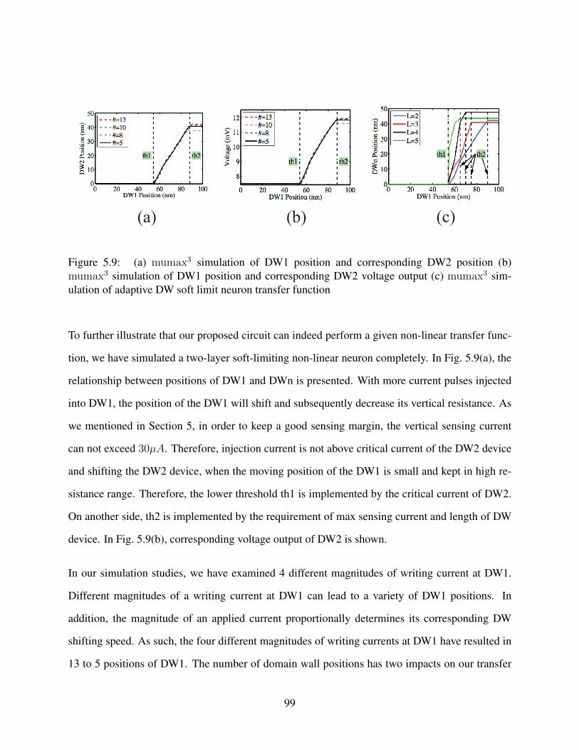
(c)(b)(a)
Figure 5.9: (a) mumax3 simulation of DW1 position and corresponding DW2 position (b)mumax3 simulation of DW1 position and corresponding DW2 voltage output (c) mumax3 sim-ulation of adaptive DW soft limit neuron transfer function
To further illustrate that our proposed circuit can indeed perform a given non-linear transfer func-
tion, we have simulated a two-layer soft-limiting non-linear neuron completely. In Fig. 5.9(a), the
relationship between positions of DW1 and DWn is presented. With more current pulses injected
into DW1, the position of the DW1 will shift and subsequently decrease its vertical resistance. As
we mentioned in Section 5, in order to keep a good sensing margin, the vertical sensing current
can not exceed 30µA. Therefore, injection current is not above critical current of the DW2 device
and shifting the DW2 device, when the moving position of the DW1 is small and kept in high re-
sistance range. Therefore, the lower threshold th1 is implemented by the critical current of DW2.
On another side, th2 is implemented by the requirement of max sensing current and length of DW
device. In Fig. 5.9(b), corresponding voltage output of DW2 is shown.
In our simulation studies, we have examined 4 different magnitudes of writing current at DW1.
Different magnitudes of a writing current at DW1 can lead to a variety of DW1 positions. In
addition, the magnitude of an applied current proportionally determines its corresponding DW
shifting speed. As such, the four different magnitudes of writing currents at DW1 have resulted in
13 to 5 positions of DW1. The number of domain wall positions has two impacts on our transfer
99

function: number of outputs and variation. For example, if DW1 has 13 positions, DW2 can output
13 different voltages. If DW1 has 5 positions, DW2 can output 5 different voltages. However,
there is a trade-off between the number of positions and its result variation. Since DW device
has a stochastic switching probability, more DW position may cause larger variation in its final
results. To implement more diverse transfer functions, we developed a multi-stage spin-based
neuron circuit by adding more DW layers. In Fig. 5.9(c), we plotted our simulation results of
different transfer functions realized by different layer numbers L.
The multi-layer architecture of our proposed neuron can significantly increase the DW velocity
for the next layer. For example, a 3-layer DWM-based neuron consists of three DWM devices
chained in series. Because each DWM device reads out its domain wall position or vertical re-
sistance though sensing its vertical current, the horizontal DW resistance is fixed by device width
and length. In our simulation, we chose the default value of horizontal DW resistance Rw to be
294.5Ω [43]. As such, the final DW layer can potentially receive a higher magnitude current from
the second layer DW device. Consequently, with the increasing number of DW layers L, the slope
of their resulting transfer function increases.
There has been some prior works, such as [77, 78, 4], that have utilized analog or digital mixed-
signal circuits to implement adaptive neuron transfer functions. However, to the best of our knowl-
edge, our proposed circuit architecture for a spin-based neuron is the first design that achieves
an adaptive soft-limiting non-linear transfer function. With CMOS-based circuit design, existing
neuron circuits often consume large power and layout size, while in the contrast, our proposed
adaptive non-linear soft-limiting neurons constructed with DWM devices can operate under very
low supplied voltage and small chip size because of 3D nature of the devices. Unfortunately,
our multi-stage circuit design for a soft-limiting non-linear transfer function does add extra signal
delay when compared with a single layer spin torque neuron. However, in the applications we
considered, such performance degradation is well justified given the enormous performance gain
100

in other aspects. For example, previous studies have shown that adaptive transfer functions can af-
ford a neural network the ability to adapt to an unknown and changing environment. Additionally,
various works [77, 78, 4] have also proven that adjustable transfer functions make on-chip learning
much more efficient as well as make a neural network more immune to high noises.
Finally, we have also considered the reliability issues associated with DWM devices in our circuit
design. One likely concern of our proposed DWM-based neuron design is its retention time after a
long period of intensive computations. Fortunately, Fukami’s recent paper has reported a 10-year
retention time at 150oC and 1014 times write endurance for Co/Ni wire, which is quite sufficient
for our targeted applications. Additionally, heating effect of DWM devices may also cause con-
cern. However, according to the analysis in [95], although the heating effect may affect the device
reliability of DWM devices, its negative impact can be effectively mitigated through appropriate
structural optimizations.
Final Piece: Flip-Flops
In conventional FPGA architecture, flip-flops are widely used as latches in configurable logic
blocks (CLBs). Recently, many research works have investigated new flip-flop architectures with
emerging devices in order to reduce hardware area and power consumption. So far, most published
circuit designs require both CMOS devices and emerging devices [109, 49, 118], and have used
MTJ devices merely as storage bits. In other words, all control logic in these proposed flip-flop
has still been implemented with the traditional CMOS devices, which, we believe, has not fully
unleashed the computing potential of emerging devices, such as MTJs. Furthermore maybe more
importantly, because our ANN circuit operates in a current mode, the conventional flip-flop de-
sign based on Boolean logic can not be used directly. In this paper, we instead propose an analog
Flip-Flop by leveraging the physical characteristics of a SHE-based DWM device.
101

DM
U
XHM-layer
T1 T2
(a)
(b)
(c)
Figure 5.10: (a) Proposed analog flip flop architecture with SHE domain wall device and CMOScontrol logic. (b) Proposed flip flop operation time diagram. (c) Spice simulation of proposedanalog flip flop according to time diagram Fig. 5.10.
102

As shown in Fig. 5.10(a), the proposed SHE DW flip-flop contains two parts, SHE DW device
and control logic. The output information from neural output node is encoded as SHE DW device
conductance through writing current at HM-layer. The Fig. 5.10 (b) shows the time diagram of
proposed flip flop. At the first Set1 domain, both of D and clock are high and turning flip-flop on
a set state. According to proposed analog flip-flop design scheme, the SHE DW device needs to
reset to original DW position before receiving a new input current D. Therefore, the large voltage
VH apply on HM-layer and generating large resetting current temperately. After short resetting
duration, the voltage applied on HM-layer switches from VH to VL for receiving new input current
D. The writing current D is larger than summation of current passing through terminal T2 and DW
critical current Ic and pushing DW moving to store input D. At the reset domain, while the input D
is low and clock is high, reset state of the flip-flop is active. The Vclk selects VL applied at terminal
T2. Since the terminal T1 connect to low input current D, the current at T2 is larger than the
summation of current T1 and DW critical current. Consequently, DW is resetting to the original
position. The Set2 and Set3 domain describe the case of two set states happened consequently. The
current D can be stored in flip-flop successful in Set3 domain, because of resetting pulse applied
before receiving the input D. The Fig. 5.10 (c) shows spice simulation results to approve proposed
architecture. The different altitude of current is encoded as DW conductance through different DW
position.
4:2 Encoder Implemented with Spin-Based LUT
To further validate our circuit design, we have performed a mixed-mode device simulation of
a 5-input-2-output MIMO-LUT design discussed in previous sections. We chose the standard
C17 benchmark circuit as our test case. The truth table of C17 benchmark circuit is obtained by
simulation results of an FPGA design.
103

3 25 26 21 17 14 19 20 28 11 8 100
0.5
1
1.5
Input neuron
Ou
tpu
t n
euro
n 11
10
10
10 10
01
1111 11 11 11
00
threhold
Figure 5.11: Simulation results of proposed truth table approximation method. The C17 truth tableis learned by proposed artificial neural network. Since the learning process has different learningerrors. In this paper, we select the best learning results. The random input number inputs toartificial neural network and procedure correct output.
We then use all inputs in this obtained truth table to train our 5-input-2-output artificial neural
network with two hidden layers and 18 hidden neurons. In Fig. 5.11, our simulation results of
this neural network that implements the C17 truth table are plotted. Note that the input values
of our neural network are generated randomly, shown in x-axes of Fig. 5.11. The corresponding
output distribution is calculated and plotted in y-axes of Fig. 5.11. A linear transfer function with
A threshold is used as the transfer function. Our simulations have shown a 100% accuracy for the
Boolean outputs of the targeted C17 circuit benchmark.
104

Logic Optimization and
Technology Mapping (ABC)
Mapped Netlist
Timing driven Packing
(T-VPACK)
Placement and Routing
(VPR)
DW Micro
Magnetic Model
( )
Circuit Netlist
BC-Netlist
Generator
BC-Netlist
Power Estimation
(fpgaEVA_LP2)
Area Delay
Circuit Model
(SPICE)
Gate
Mapping
(.genlib)
Power
Figure 5.12: Customized CAD flow for SN-FPGA.
Performance Analysis and Comparison
To validate the performance benefits of our proposed SN-FPGA architecture, we not only have
modified the standard LUT-based FPGA CAD flow [12] but also added several mixed-mode sim-
ulation modules in order to accurately model the circuit behavior of SN-FPGA. In Fig.5.12, we
have shown all necessary building blocks of our CAD flow with the input as a benchmark circuit.
45nm CMOS was chosen as the reference technology node and was modelled with the Berkeley
105

Predictive Technology Model (BPTM) [15] for both devices and interconnects. As in [72], we as-
sume an island-style FPGA as the baseline architecture, referred to henceforth as baseline FPGA,
for our performance comparison. It comprises a 2D array of Logic Blocks (LBs) interconnected
via programmable routing. We assume each LB comprises four logic slices, each consisting of
two 4-input Lookup Tables (LUTs), two Flip-Flops (FFs), and programming overhead. The rout-
ing fabric comprises horizontal and vertical routing channels each having sets of Single, Double,
HEX-3, and HEX-6 interconnect segments. We classify the interconnects into two groups, short,
which includes Single and Double FPGA tile width interconnects, and long, which includes HEX-
3 and HEX-6 interconnects. The segments can be connected to the inputs and outputs of the LBs
via connection boxes and to each other via switch boxes. We assume the MUX-based switch box
design described in [68]. Similar to conventional FPGA device, there is a trade-off between the
approximation capacity and the learning speed of a neural network. The larger hidden neuron
number ensure larger truth table to approximate, however, lower learning speed.
LUT Size K=4 LUT Size K=5 LUT Size K=60
2000
4000
6000
8000
10000
12000
14000
16000
18000
# o
f N
odes
O=1
O=2
O=3
O=4
O=1
O=2
O=3
O=4
O=1
O=2
O=3
O=4
alu4
apex4
clma
frisc
Figure 5.13: ABC synthesis results of four different benchmark circuit with different LUT size andoutput bits. The usage of multi-output bits will decrease the number of nodes dramatically.
106

Our proposed SN-FPGA architecture utilizes a standard 45nm CMOS technology node and SHE
domain wall devices. For the proposed architecture, we choose four benchmark circuits to first
determine the input number m and output number n for each all spin neural network logic block.
The logic synthesis and technology mapping for a given benchmark was conducted with a modified
version of the ABC tool based on computing the full covering with (k, l)-cuts. As shown in
Fig. 5.13, with the output number of all spin neural network logic block increasing, for all four
benchmarks, the total number of all spin neural network logic block will decrease significantly.
Not surprisingly, when we increase the input numbers, the total number of all spin neural network
logic block also decreases. These results are also used in performance measurement.
To accurately measure the chip area of all FPGA architectures we compared, we adopted two
different methodologies. For the 2D island-style FPGA, we used the area modelling method at
the transistor level, which was first developed in [11, 2]. The based FPGA is first decomposed
into components including SRAM based LUTs, flip-flops, intracluster muxes, intercluster routing
muxes and switches. The chip area of each of these components is then estimated by counting the
total number of minimum-width transistors used. For the SN-FPGA implemented with the hybrid
MTJ-CMOS technology, we have to account for its “3D effect”. Fortunately, one of VPR’s advan-
tages is its flexibility. It supports different FPGA architecture explorations. The new architecture
can be easily refined in VPR’s architecture file. In order to evaluate our chip area, we enhanced the
existing 2D FPGA architecture with 3D related options to make a new 3D FPGA architecture. The
area parameters of a single artificial neural network block are defined based on the sizes of DWM
devices reported in [35, 92].
Compared with ASIC, the conventional FPGA has sacrificed performance for programmability. In
fact, the routing structure of a conventional FPGA consumes the majority (sometimes more than
80%) of hardware resource [24]. In our proposed SN-FPGA architecture, besides the saving of
reconfigurable logic blocks, the usage of multiple-input-multiple-output spin-based neural network
107
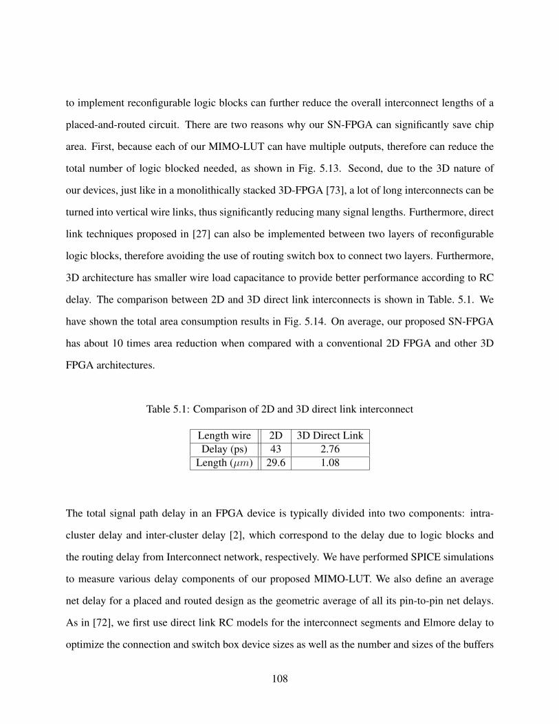
to implement reconfigurable logic blocks can further reduce the overall interconnect lengths of a
placed-and-routed circuit. There are two reasons why our SN-FPGA can significantly save chip
area. First, because each of our MIMO-LUT can have multiple outputs, therefore can reduce the
total number of logic blocked needed, as shown in Fig. 5.13. Second, due to the 3D nature of
our devices, just like in a monolithically stacked 3D-FPGA [73], a lot of long interconnects can be
turned into vertical wire links, thus significantly reducing many signal lengths. Furthermore, direct
link techniques proposed in [27] can also be implemented between two layers of reconfigurable
logic blocks, therefore avoiding the use of routing switch box to connect two layers. Furthermore,
3D architecture has smaller wire load capacitance to provide better performance according to RC
delay. The comparison between 2D and 3D direct link interconnects is shown in Table. 5.1. We
have shown the total area consumption results in Fig. 5.14. On average, our proposed SN-FPGA
has about 10 times area reduction when compared with a conventional 2D FPGA and other 3D
FPGA architectures.
Table 5.1: Comparison of 2D and 3D direct link interconnect
Length wire 2D 3D Direct LinkDelay (ps) 43 2.76
Length (µm) 29.6 1.08
The total signal path delay in an FPGA device is typically divided into two components: intra-
cluster delay and inter-cluster delay [2], which correspond to the delay due to logic blocks and
the routing delay from Interconnect network, respectively. We have performed SPICE simulations
to measure various delay components of our proposed MIMO-LUT. We also define an average
net delay for a placed and routed design as the geometric average of all its pin-to-pin net delays.
As in [72], we first use direct link RC models for the interconnect segments and Elmore delay to
optimize the connection and switch box device sizes as well as the number and sizes of the buffers
108

for the HEX-3 and HEX-6 segments for a given FPGA array size in each technology node.
alu4 apex2 apex4 clma diffeq elliptic ex1010 ex5p frisc misex3 pdc s2981
10
100
1000
Are
a (1
04µ
m2)
CMOS
3DCMOS
3D rFPGA
SNFPGA
Figure 5.14: The area comparison of different FPGA architecture[24, 27, 75]
We then use this modified version of the VPR delay calculation function to compute net delays.
The net delay calculation results are then used in the 3D architecture file in VPR generation. The
parameters we changed in the architecture file include: the max limit of number of 3D interconnect
in a tile, a number of wires are connected to vertical, and resistance and capacitance value of 3D
interconnect.
In conventional FPGA architecture, the total critical path delay is defined as the delay according
to logic cluster combined with the routing delay. The paper [2] claimed that increasing LUT size
or number of LUTs in a cluster decreases the critical path delay. For example, while conventional
FPGA has 1 LUT size and 2 LUTs in a cluster, the average delay of 28 ISCAS-85 benchmark
circuits are 45ns. For LUT size is 7 and 2 LUTs in a cluster architecture, the critical delay is
just 14ns. On another side, the proposed all spin artificial neural network based FPGA has highly
parallel architecture. The 3 layer artificial neural network can approximate any truth tables by
adding parallel input, hidden, and output nodes parallelly. As shown in the previous section, larger
current to SHE-assist neuron can increase the switching speed.
109

alu4 apex2 apex4 clma diffeq elliptic ex1010 ex5p frisc misex3 pdc s2980
5
10
15
Del
ay (
ns)
CMOS
3DCMOS
3D rFPGA
SNFPGA
Figure 5.15: Delay comparisons between different FPGA architectures[24, 27, 75]
DW velocities of more than 400 m/s have been demonstrated in the literature[80], hence, for a 40
nm long free domain, more than 1 GHz processing speed may be achievable. In this paper the SHE
has been explored for bringing a large reduction in DW current thresholds[42]. Such a phenomena
can be exploited to improve the resolution of scaled domain wall devices. In Fig. 5.15, the delay
comparison results between different FPGA architectures are shown. In general, our proposed SN-
FPGA has much less delay than CMOS conventional FPGA design. To compare with others 3D
emerging FPGA architectures, we have two different results. For some of the complex benchmark
circuits, our proposed SN-FPGA has smaller delay than both 2D and 3D FPGA architecture. This
is because of the larger reduction in the number of used reconfigurable logic blocks. However, for
some really simple benchmark circuits, our proposed architecture actually has worse performance
because of the delay of spin torque devices. Without a large reduction in the number of nodes, the
delay performance of an SN-FPGA could be worse than others 3D emerging FPGA architectures.
When quantifying the energy consumption of an SN-FPGA device, its static power consumption
can be neglected due to the spin torque device characteristics[35]. In fact, the power consumption
of a SN-FPGA device is typically dominated by all active spin-based neurons, which has two
110

components: switching and reading. The switching energy is due to its writing current flows
through the DWM-based neurons. This energy is equal to the product of the combined current
passing through all spin synapses and the neuron switch time. In our case, the average input current
is around 50µA, which is equivalent to input voltage level of 50mV. Therefore, the average energy
consumption of each spin-based neuron is about 2.5fJ. If we consider on-chip supply distribution
schemes, the minimum input voltage is required for noise consideration. However, if we increase
writing current to 100mV, the switching energy of neuron is still small and limited to 5fJ. The
second part energy consumption is caused by the read operation in spin-based neurons. For a
supply voltage of 0.8V, this energy consumption would evaluate to be 0.48fJ. In conclusion, the
total energy dissipation of spin neuron for average switch speed by input current 50µA would be
3fJ.
alu4 apex2 apex4 clma diffeq elliptic ex1010 ex5p frisc misex3 pdc s2980
80
160
Pow
er (
mW
)
CMOS
3DCMOS
3D rFPGA
SNFPGA
Figure 5.16: Power comparison of different FPGA architecture[24, 27, 76]
The power comparison results between different FPGA architectures are shown in Fig. 5.16. we
have compared the performance of our proposed SN-FPGA against three other FPGA architectures
using the 45nm CMOS technology node and the Perpentidular Magnetic Anistrophy (PMA) MTJ
Compact model [106]. The first FPGA is a typical 2D island-style architecture implemented with
45 nm CMOS technology. The second architecture is based on the work in [76], where a nano
111

crossbar architecture is used to replace the conventional NVFM for high density and lower power
consumption. The third FPGA is a 3D rFPGA first presented in [76] that utilizes high-density
resistive memory (RRAM) to build FPGA components. Different from the existing CMOS-nano
hybrid circuits that use crossbars, the proposed rFPGA structures consist of mainly 1T1R structures
(1 CMOS transistor is integrated with a two-terminal resistive nanojunction) that can be fabricated
using a CMOS-compatible process. Our software tool chain is mostly based on the well-know
VPR package from the University of Toronto and a modified version of ABC from UC Berkeley.
In particular, our power analysis is carried out through the power evaluator, fpgaEvaLP2 [69].
Not surprisingly, the conventional FPGA based in the 45nm device technology consumes the high-
est power mainly because of the routing interconnects and programmable switches. Secondly, the
relatively low utilization rate (∼ 12%) of FPGA logic fabric significantly reduces its efficiency.
Our proposed SN-FPGA achieves the highest energy efficiency. There are several contributing
factors. First, emerging devices can be constructed in a 3D metallic structure, therefore drastically
reducing the energy dissipation of all interconnects. Second, emerging devices can be operated
with ultra-low currents for reading and writing procedure (few µAs). Moreover, static power dissi-
pation almost vanishes due to its non-volatile character. Third, small MIMO neural network blocks
can result in very high energy and area efficiency by reducing routing resource.
Conclusion
With the spintronic device technology surging into the mainstream, how to rethink and redesign
the existing FPGA architecture is a fascinating yet challenging research problem. This paper is a
first step towards capitalizing on the spintronic device technology natively for direct logic compu-
tations. Our Spin-based Neural Field Programmable Gate Array (SN-FPGA) architecture deviates
from the conventional FPGA architecture by directly utilizing the stochastic switching behavior
112

of emerging device technology for Boolean logic computing, while going beyond simply utilizing
spintronic devices as an alternative memory technology.
113

CHAPTER 6: CONCLUSION
In this dissertation, the beyond von-neumann, bio-inspired non-boolean computing schemes are
proposed. In recent decades, the increasing demand for high performance hardware with fast
speed, large-capacity, energy efficient computing platforms is being widely investigated. Spin-
tronic device is considering as a promising device for this purpose. With the spintronic device
technology surging into the mainstream, how to rethink and redesign the existing computing ar-
chitecture is a fascinating yet challenging research problem. Directly replacement of CMOS with
spintronic device does not maximise the benefits. This paper is a first step towards capitalizing on
the spintronic device technology natively non-traditional computing technologies.
In order to achieve natievly non-traditional computing technologies, we presented three computing
paradigms based on spintronic device.
Using emerging spintronic devices, we propose a Domain-Wall-Motion-based NCL circuit de-
sign methodology that achieves approximately 30x and 8x improvements in energy efficiency and
chip layout area, respectively, over its equivalent CMOS design, while maintaining a similar de-
lay performance for a 32-bit full adder. These advantages are made possible mostly by exploiting
the domain wall motion physics to natively realize the hysteresis critically needed in NCL. More
Interestingly, this design choice achieves ultra-high robustness by allowing spintronic device pa-
rameters to vary within a predetermined range while still achieving correct operations.
Next, we propose an innovative stochastic-based computing architecture to implement low-power
and robust artificial neural network (S-ANN) with both magnetic tunneling junction (MTJ) and do-
main wall motion (DWM) devices. Our mixed model HSPICE simulation results have shown that,
for a well known pattern recognition task, a 34-neuron S-ANN implementation achieves more than
1.5 orders of magnitude lower energy consumption and 2.5 orders of magnitude less hidden layer
114

chip area, when compared with its deterministic-based ANN counterparts implemented with digi-
tal and analog CMOS circuits. We believe that our S-ANN architecture achieves such a remarkable
performance gain by leveraging two key ideas. First, because all neural signals are encoded as ran-
dom bit streams, the standard weighed-sum synapses can be accomplished by stochastic bit writing
and reading procedure. Second, we designed and implemented a novel multiple-phase pumping
circuit structure to effectively realize the soft-limiting neural transfer function that is essential to
improve the overall ANN capability and reduce its network complexity.
Finally, we describe Spin Torque based Neural Field Programmable Gate Array (SNFPGA), an
innovative architecture attempting to exploit the stochastic switching behavior newly found in
emerging spintronic devices for reconfigurable computing. While many recent studies have inves-
tigated using Spin Transfer Torque Memory (STTM) devices to replace configuration memory in
FPGAs, our study, for the first time, attempts to use the quantum-induced approximation property
exhibited by spintronic devices directly for reconfiguration and logic computation. Specifically,
the SNFPGA was designed from scratch for high performance, routability, and ease-of-use. It sup-
ports variable-granularity multiple-input-multiple-output (MIMO) logic blocks and variable-length
bypassing interconnects with a symmetrical structure. Due to its unconventional architectural fea-
tures, the SNFPGA requires several major modifications to be made in the standard VPR place-
ment/routing CAD flow, which include a new technology mapping algorithm based on computing
(k, l)-cut, a new placement algorithm, and a modified delay-based routing procedure. Previous
studies have shown that simply replacing reconfiguration memory bits with spintronic devices, the
conventional 2D island-style FPGA architecture can achieve approximately 10x area savings, 1.5x
speedup and 3x power savings for the 12 benchmark circuits over an island-style baseline FPGA
with spintronic configuration bits.
115

LIST OF REFERENCES
[1] Actel, Inc. Automotive ProASIC3 flash family FPGAs datasheet, March 2007.
[2] E. Ahmed and J. Rose. The effect of lut and cluster size on deep-submicron FPGA perfor-
mance and density. Very Large Scale Integration (VLSI) Systems, IEEE Transactions on,
12(3):288–298, March 2004.
[3] C. Alippi. Selecting accurate, robust, and minimal feedforward neural networks. Circuits
and Systems I: Fundamental Theory and Applications, IEEE Transactions on, 49(12):1799–
1810, Dec 2002.
[4] Andrew R Barron. Universal approximation bounds for superpositions of a sigmoidal func-
tion. Information Theory, IEEE Transactions on, 39(3):930–945, 1993.
[5] IA Basheer and M Hajmeer. Artificial neural networks: fundamentals, computing, design,
and application. Journal of microbiological methods, 43(1):3–31, 2000.
[6] Ismet Bayraktaroglu, Arif Selcuk Ogrenci, Gunhan Dundar, Sina Balkır, and Ethem Al-
paydın. Annsys: an analog neural network synthesis system. Neural Networks, 12(2):325–
338, 1999.
[7] Peter A. Beerel, Recep O. Ozdag, and Marcos Ferretti. A Designer’s Guide to Asynchronous
VLSI. Cambridge University Press, New York, NY, USA, 1st edition, 2010.
[8] M.R Belli, M Conti, P Crippa, and C Turchetti. Artificial neural networks as approximators
of stochastic processes. Neural Networks, 12(45):647 – 658, 1999.
[9] A. Bermak and D. Martinez. A compact 3d vlsi classifier using bagging threshold network
ensembles. Neural Networks, IEEE Transactions on, 14(5):1097–1109, Sept 2003.
116
[10] K. Bernstein, R. K. Cavin, W. Porod, A. Seabaugh, and J. Welser. Device and architecture
outlook for beyond cmos switches. Proceedings of the IEEE, 98(12):2169–2184, Dec 2010.
[11] Vaughn Betz and Jonathan Rose. FPGA routing architecture: segmentation and buffering to
optimize speed and density. In Proceedings of the 1999 ACM/SIGDA Seventh International
Symposium on Field-Programmable Gate Arrays, pages 59 – 68, 1999.
[12] Vaughn Betz, Jonathan Rose, and Alexander Marquardt, editors. Architecture and CAD for
Deep-Submicron FPGAs. Kluwer Academic Publishers, Norwell, MA, USA, 1999.
[13] Julien Borghetti, Gregory S Snider, Philip J Kuekes, J Joshua Yang, Duncan R Stewart,
and R Stanley Williams. memristiveswitches enable statefullogic operations via material
implication. Nature, 464(7290):873–876, 2010.
[14] Bradley D Brown and Howard C Card. Stochastic neural computation. ii. soft competitive
learning. Computers, IEEE Transactions on, 50(9):906–920, 2001.
[15] Y. Cao, T. Sato, M. Orshansky, D. Sylvester, and C. Hu. New paradigm of predictive mos-
fet and interconnect modeling for early circuit simulation. In Custom Integrated Circuits
Conference, 2000. CICC. Proceedings of the IEEE 2000, pages 201–204, 2000.
[16] D. Chabi, W. Zhao, D. Querlioz, and J. O. Klein. Robust neural logic block (nlb) based
on memristor crossbar array. In Nanoscale Architectures (NANOARCH), 2011 IEEE/ACM
International Symposium on, pages 137–143, June 2011.
[17] A Chanthbouala, R Matsumoto, J Grollier, V Cros, A Anane, A Fert, AV Khvalkovskiy,
KA Zvezdin, K Nishimura, Y Nagamine, et al. Vertical-current-induced domain-wall mo-
tion in mgo-based magnetic tunnel junctions with low current densities. Nature Physics,
7(8):626–630, 2011.
117

[18] An Chen. Accessibility of nano-crossbar arrays of resistive switching devices. In Nanotech-
nology (IEEE-NANO), 2011 11th IEEE Conference on, pages 1767–1771, Aug 2011.
[19] Te-Hsuan Chen, Armin Alaghi, and John P Hayes. Behavior of stochastic circuits under
severe error conditions. it-Information Technology, 56(4):182–191, 2014.
[20] Won Ho Choi, Yang Lv, Jongyeon Kim, A. Deshpande, Gyuseong Kang, Jian-Ping Wang,
and C. H. Kim. A magnetic tunnel junction based true random number generator with
conditional perturb and real-time output probability tracking. In 2014 IEEE International
Electron Devices Meeting, pages 12.5.1–12.5.4, Dec 2014.
[21] Won Ho Choi, L.V. Yang, Jongyeon Kim, A. Deshpande, Gyuseong Kang, Jian-Ping Wang,
and C.H. Kim. A magnetic tunnel junction based true random number generator with con-
ditional perturb and real-time output probability tracking. In Electron Devices Meeting
(IEDM), 2014 IEEE International, pages 12.5.1–12.5.4, Dec 2014.
[22] L.O. Chua and L. Yang. Cellular neural networks: theory. Circuits and Systems, IEEE
Transactions on, 35(10):1257–1272, Oct 1988.
[23] Sungwoo Chun, Seung-Beck Lee, Masahiko Hara, Wanjun Park, and Song-Ju Kim. High-
density physical random number generator using spin signals in multidomain ferromagnetic
layer. Advances in Condensed Matter Physics, 2015, 2015.
[24] J. Cong and Bingjun Xiao. mrfpga: A novel fpga architecture with memristor-based recon-
figuration. In 2011 IEEE/ACM International Symposium on Nanoscale Architectures, pages
1–8, June 2011.
[25] R. Dlugosz, T. Talaska, and W. Pedrycz. Current-mode analog adaptive mechanism for ultra-
low-power neural networks. Circuits and Systems II: Express Briefs, IEEE Transactions on,
58(1):31–35, Jan 2011.
118

[26] J. Dobes, L. Pospisil, and A. Yadav. Precise characterization of memristive systems by
cooperative artificial neural networks. In Soft Computing and Intelligent Systems (SCIS)
and 13th International Symposium on Advanced Intelligent Systems (ISIS), 2012 Joint 6th
International Conference on, pages 2130–2133, Nov 2012.
[27] Chen Dong, Chen Chen, Subhasish Mitra, and Deming Chen. Architecture and performance
evaluation of 3d cmos-nem fpga. In Proceedings of the System Level Interconnect Prediction
Workshop, SLIP ’11, pages 2:1–2:8, Piscataway, NJ, USA, 2011. IEEE Press.
[28] Idongesit E Ebong and Pinaki Mazumder. Cmos and memristor-based neural network design
for position detection. Proceedings of the IEEE, 100(6):2050–2060, 2012.
[29] I.E. Ebong and P. Mazumder. Self-controlled writing and erasing in a memristor crossbar
memory. Nanotechnology, IEEE Transactions on, 10(6):1454–1463, Nov 2011.
[30] Satoru Emori, Uwe Bauer, Sung-Min Ahn, Eduardo Martinez, and Geoffrey SD Beach.
Current-driven dynamics of chiral ferromagnetic domain walls. Nature materials,
12(7):611–616, 2013.
[31] Satoru Emori, Eduardo Martinez, Kyung-Jin Lee, Hyun-Woo Lee, Uwe Bauer, Sung-Min
Ahn, Parnika Agrawal, David C Bono, and Geoffrey SD Beach. Spin hall torque magne-
tometry of dzyaloshinskii domain walls. Physical Review B, 90(18):184427, 2014.
[32] Deliang Fan. Boolean and brain-inspired computing using spin-transfer torque devices.
PhD thesis, PURDUE UNIVERSITY, 2015.
[33] Deliang Fan, Supriyo Maji, Karthik Yogendra, Mrigank Sharad, and Kaushik Roy.
Injection-locked spin hall-induced coupled-oscillators for energy efficient associative com-
puting. Nanotechnology, IEEE Transactions on, 14(6):1083–1093, 2015.
119

[34] Deliang Fan, Mrigank Sharad, and Kaushik Roy. Design and synthesis of ultralow energy
spin-memristor threshold logic. Nanotechnology, IEEE Transactions on, 13(3):574–583,
2014.
[35] Deliang Fan, Mrigank Sharad, Abhronil Sengupta, and Kaushik Roy. Hierarchical temporal
memory based on spin-neurons and resistive memory for energy-efficient brain-inspired
computing. arXiv preprint arXiv:1402.2902, 2014.
[36] Deliang Fan, Yong Shim, Anand Raghunathan, and Kaushik Roy. STT-SNN: A spin-
transfer-torque based soft-limiting non-linear neuron for low-power artificial neural net-
works. CoRR, abs/1412.8648, 2014.
[37] Deliang Fan, Yong Shim, Anand Raghunathan, and Kaushik Roy. Stt-snn: A spin-transfer-
torque based soft-limiting non-linear neuron for low-power artificial neural networks. arXiv
preprint arXiv:1412.8648, 2014.
[38] Michael Feigenson, James W. Reiner, and Lior Klein. Efficient current-induced domain-
wall displacement in srruo3. Phys. Rev. Lett., 98:247204, Jun 2007.
[39] Xuanyao Fong, Mei-Chin Chen, and K. Roy. Generating true random numbers using on-
chip complementary polarizer spin-transfer torque magnetic tunnel junctions. In Device
Research Conference (DRC), 2014 72nd Annual, pages 103–104, June 2014.
[40] Xuanyao Fong, S.K. Gupta, N.N. Mojumder, S.H. Choday, C. Augustine, and K. Roy.
Knack: A hybrid spin-charge mixed-mode simulator for evaluating different genres of spin-
transfer torque mram bit-cells. In Simulation of Semiconductor Processes and Devices (SIS-
PAD), 2011 International Conference on, pages 51–54, Sept 2011.
[41] Xuanyao Fong, Sumeet K Gupta, Niladri N Mojumder, Sri Harsha Choday, Charles Augus-
tine, and Kaushik Roy. Knack: A hybrid spin-charge mixed-mode simulator for evaluating
120

different genres of spin-transfer torque mram bit-cells. In Simulation of Semiconductor
Processes and Devices (SISPAD), 2011 International Conference on, pages 51–54. IEEE,
2011.
[42] S. Fukami, Y. Nakatani, T. Suzuki, K. Nagahara, N. Ohshima, and N. Ishiwata. Relation
between critical current of domain wall motion and wire dimension in perpendicularly mag-
netized co/ni nanowires. Applied Physics Letters, 95(23):–, 2009.
[43] S. Fukami, M. Yamanouchi, K.-J. Kim, T. Suzuki, N. Sakimura, D. Chiba, S. Ikeda, T. Sug-
ibayashi, N. Kasai, T. Ono, and H. Ohno. 20-nm magnetic domain wall motion memory with
ultralow-power operation. In Electron Devices Meeting (IEDM), 2013 IEEE International,
pages 3.5.1–3.5.4, Dec 2013.
[44] S. Fukami, M. Yamanouchi, T. Koyama, K. Ueda, Y. Yoshimura, K.-J. Kim, D. Chiba,
H. Honjo, N. Sakimura, R. Nebashi, Y. Kato, Y. Tsuji, A. Morioka, K. Kinoshita, S. Miura,
T. Suzuki, H. Tanigawa, S. Ikeda, T. Sugibayashi, N. Kasai, T. Ono, and H. Ohno. High-
speed and reliable domain wall motion device: Material design for embedded memory and
logic application. In VLSI Technology (VLSIT), 2012 Symposium on, pages 61–62, June
2012.
[45] S. Fukami, M. Yamanouchi, T. Koyama, K. Ueda, Y. Yoshimura, K.-J. Kim, D. Chiba,
H. Honjo, N. Sakimura, R. Nebashi, Y. Kato, Y. Tsuji, A. Morioka, K. Kinoshita, S. Miura,
T. Suzuki, H. Tanigawa, S. Ikeda, T. Sugibayashi, N. Kasai, T. Ono, and H. Ohno. High-
speed and reliable domain wall motion device: Material design for embedded memory and
logic application. In VLSI Technology (VLSIT), 2012 Symposium on, pages 61–62, June
2012.
121

[46] Akio Fukushima, Takayuki Seki, Kay Yakushiji, Hitoshi Kubota, Hiroshi Imamura, Shinji
Yuasa, and Koji Ando. Spin dice: A scalable truly random number generator based on
spintronics. Applied Physics Express, 7(8):083001, 2014.
[47] Rafael Gadea, Joaquın Cerda, Franciso Ballester, and Antonio Mocholı. Artificial neu-
ral network implementation on a single fpga of a pipelined on-line backpropagation. In
Proceedings of the 13th International Symposium on System Synthesis, ISSS ’00, pages
225–230, Washington, DC, USA, 2000. IEEE Computer Society.
[48] AS Grove. Changing vectors of moore?s law. In Keynote speech, International Electron
Devices Meeting, 2002.
[49] Michael Hall, Albrecht Jander, Roger D Chamberlain, and Pallavi Dhagat. Globally clocked
magnetic logic circuits. 2009.
[50] A. Hirohata, H. Sukegawa, H. Yanagihara, I. uti, T. Seki, S. Mizukami, and R. Swaminathan.
Roadmap for emerging materials for spintronic device applications. IEEE Transactions on
Magnetics, 51(10):1–11, Oct 2015.
[51] John J Hopfield. Artificial neural networks. Circuits and Devices Magazine, IEEE, 4(5):3–
10, 1988.
[52] Miao Hu, Yu Wang, Qinru Qiu, Yiran Chen, and Hai Li. The stochastic modeling of tio2
memristor and its usage in neuromorphic system design. In Design Automation Conference
(ASP-DAC), 2014 19th Asia and South Pacific, pages 831–836, Jan 2014.
[53] Guang-Bin Huang. Learning capability and storage capacity of two-hidden-layer feedfor-
ward networks. IEEE Transactions on Neural Networks, 14(2):274–281, Mar 2003.
[54] Paolo Ienne. Digital hardware architectures for neural networks. Speedup Journal, 1(9),
1995.
122

[55] S Ikeda, J Hayakawa, Y Ashizawa, YM Lee, K Miura, H Hasegawa, M Tsunoda, F Mat-
sukura, and H Ohno. Tunnel magnetoresistance of 604% at 300 k by suppression of ta
diffusion in cofeb/mgo/cofeb pseudo-spin-valves annealed at high temperature. Applied
Physics Letters, 93(8):2508, 2008.
[56] Cheoljoo Jeong and S.M. Nowick. Optimal technology mapping and cell merger for asyn-
chronous threshold networks. In Asynchronous Circuits and Systems, 2006. 12th IEEE
International Symposium on, pages 10 pp.–137, March 2006.
[57] Yuan Ji, Feng Ran, Cong Ma, and D.J. Lilja. A hardware implementation of a radial ba-
sis function neural network using stochastic logic. In Design, Automation Test in Europe
Conference Exhibition (DATE), 2015, pages 880–883, March 2015.
[58] Sung Hyun Jo, Ting Chang, Idongesit Ebong, Bhavitavya B. Bhadviya, Pinaki Mazumder,
and Wei Lu. Nanoscale memristor device as synapse in neuromorphic systems. Nano
Letters, 10(4):1297–1301, 2010. PMID: 20192230.
[59] H. Kim, M. P. Sah, C. Yang, T. Roska, and L. O. Chua. Memristor bridge synapses. Pro-
ceedings of the IEEE, 100(6):2061–2070, June 2012.
[60] Kuk-Hwan Kim, Siddharth Gaba, Dana Wheeler, Jose M Cruz-Albrecht, Tahir Hussain,
Narayan Srinivasa, and Wei Lu. A functional hybrid memristor crossbar-array/cmos system
for data storage and neuromorphic applications. Nano letters, 12(1):389–395, 2011.
[61] Yusung Kim, Xuanyao Fong, Kon-Woo Kwon, Mei-Chin Chen, and K. Roy. Multilevel
spin-orbit torque mrams. Electron Devices, IEEE Transactions on, 62(2):561–568, Feb
2015.
[62] M. Kolasa and R. Dlugosz. An advanced software model for optimization of self-organizing
neural networks oriented on implementation in hardware. In Mixed Design of Integrated
123
Circuits Systems (MIXDES), 2015 22nd International Conference, pages 266–271, June
2015.
[63] T. Kosel, P. Jeavons, and J. Shawe-Taylor. Emergent activation functions from a stochastic
bit-stream neuron. Electronics Letters, 30(4):331–333, Feb 1994.
[64] Tomohiro Koyama, Kohei Ueda, K-J Kim, Yoko Yoshimura, Daichi Chiba, Keisuke Ya-
mada, J-P Jamet, Alexandra Mougin, Andre Thiaville, Shigemi Mizukami, et al. Current-
induced magnetic domain wall motion below intrinsic threshold triggered by walker break-
down. Nature nanotechnology, 7(10):635–639, 2012.
[65] Mohamad T Krounbi, S Watts, D Apalkov, X Tangm K Moonm V Nikitin, A Ong, and
E Chen. Status and challenges for non-volatile spin-transfer torque ram (stt-ram). In Inter-
national Symposium on Advanced Gate Stack Technology Albany, 2010.
[66] S.Y. Kung. Digital Neural Networks. Information and system sciences series. Prentice Hall,
1993.
[67] S. Kvatinsky, K. Talisveyberg, D. Fliter, A. Kolodny, U.C. Weiser, and E.G. Friedman.
Models of memristors for spice simulations. In Electrical Electronics Engineers in Israel
(IEEEI), 2012 IEEE 27th Convention of, pages 1–5, Nov 2012.
[68] Guy Lemieux and David Lewis. Circuit design of routing switches. In Proceedings of the
2002 ACM/SIGDA Tenth International Symposium on Field-Programmable Gate Arrays,
pages 19 – 28, 2002.
[69] Fei Li, Yan Lin, Lei He, Deming Chen, and J. Cong. Power modeling and characteristics of
field programmable gate arrays. Computer-Aided Design of Integrated Circuits and Systems,
IEEE Transactions on, 24(11):1712–1724, Nov 2005.
124

[70] Hui Li, Da Zhang, and S.Y. Foo. A stochastic digital implementation of a neural net-
work controller for small wind turbine systems. Power Electronics, IEEE Transactions
on, 21(5):1502–1507, Sept 2006.
[71] Michiel Ligthart, Karl Fant, Ross Smith, Alexander Taubin, and Alex Kondratyev. Asyn-
chronous design using commercial hdl synthesis tools. In Proceedings of the 6th Interna-
tional Symposium on Advanced Research in Asynchronous Circuits and Systems, ASYNC
’00, pages 114–, Washington, DC, USA, 2000. IEEE Computer Society.
[72] Mingjie Lin and Abbas El Gamal. A routing fabric for monolithically stacked 3D-FPGA.
In Proceedings of the 2007 ACM/SIGDA 15th International Symposium on Field Pro-
grammable Gate Arrays, FPGA ’07, pages 3–12, New York, NY, USA, 2007. ACM.
[73] Mingjie Lin, Abbas El Gamal, Yi-Chang Lu, and Simon Wong. Performance benefits of
monolithically stacked 3D-FPGA. In Proceedings of the 2006 ACM/SIGDA Tenth Interna-
tional Symposium on Field-Programmable Gate Arrays, pages 113 – 122, 2006.
[74] YiChing Lin, SH Kang, YJ Wang, K Lee, X Zhu, WC Chen, X Li, WN Hsu, YC Kao,
MT Liu, et al. 45nm low power cmos logic compatible embedded stt mram utilizing a
reverse-connection 1t/1mtj cell. In Electron Devices Meeting (IEDM), 2009 IEEE Interna-
tional, pages 1–4. IEEE, 2009.
[75] Ming Liu and Wei Wang. rfga: Cmos-nano hybrid fpga using rram components. In 2008
IEEE International Symposium on Nanoscale Architectures, pages 93–98, June 2008.
[76] Ming Liu and Wei Wang. rFGA: Cmos-nano hybrid FPGA using RRAM components. 2013
IEEE/ACM International Symposium on Nanoscale Architectures (NANOARCH), 0:93–98,
2008.
125

[77] Chun Lu and Bingxue Shi. Circuit design of an adjustable neuron activation function and
its derivative. Electronics Letters, 36(6):553–555, Mar 2000.
[78] M. Martincigh and A. Abramo. A new architecture for digital stochastic pulse-mode neurons
based on the voting circuit. IEEE Transactions on Neural Networks, 16(6):1685–1693, Nov
2005.
[79] Eduardo Martinez, Satoru Emori, Noel Perez, Luis Torres, and Geoffrey SD Beach. Current-
driven dynamics of dzyaloshinskii domain walls in the presence of in-plane fields: Full
micromagnetic and one-dimensional analysis. Journal of Applied Physics, 115(21):213909,
2014.
[80] Peter J Metaxas, Joao Sampaio, Andre Chanthbouala, Rie Matsumoto, Abdelmadjid Anane,
Albert Fert, Konstantin A Zvezdin, Kay Yakushiji, Hitoshi Kubota, Akio Fukushima, et al.
High domain wall velocities via spin transfer torque using vertical current injection. Scien-
tific reports, 3, 2013.
[81] T. Nandha Kumar, H.A.F. Almurib, and F. Lombardi. On the operational features and per-
formance of a memristor-based cell for a lut of an fpga. In Nanotechnology (IEEE-NANO),
2013 13th IEEE Conference on, pages 71–76, Aug 2013.
[82] N. Nedjah and L. de Macedo Mourelle. Stochastic reconfigurable hardware for neural net-
works. In Digital System Design, 2003. Proceedings. Euromicro Symposium on, pages
438–442, Sept 2003.
[83] N. Onizawa, D. Katagiri, W.J. Gross, and T. Hanyu. Analog-to-stochastic converter us-
ing magnetic-tunnel junction devices. In Nanoscale Architectures (NANOARCH), 2014
IEEE/ACM International Symposium on, pages 59–64, July 2014.
126
[84] Ernesto Ordonez Cardenas and Rene de J. Romero-Troncoso. Mlp neural network and on-
line backpropagation learning implementation in a low-cost fpga. In Proceedings of the 18th
ACM Great Lakes Symposium on VLSI, GLSVLSI ’08, pages 333–338, 2008.
[85] G. Palma, M. Suri, D. Querlioz, E. Vianello, and B. De Salvo. Stochastic neuron design
using conductive bridge ram. In Nanoscale Architectures (NANOARCH), 2013 IEEE/ACM
International Symposium on, pages 95–100, July 2013.
[86] F.A. Parsan, W.K. Al-Assadi, and S.C. Smith. Gate mapping automation for asynchronous
null convention logic circuits. Very Large Scale Integration (VLSI) Systems, IEEE Transac-
tions on, 22(1):99–112, Jan 2014.
[87] Farhad A. Parsan and Scott C. Smith. Cmos implementation of static threshold gates with
hysteresis: A new approach. In VLSI and System-on-Chip, 2012 (VLSI-SoC), IEEE/IFIP
20th International Conference on, pages 41–45, Oct 2012.
[88] Farhad A Parsan and Scott C Smith. Cmos implementation of threshold gates with hystere-
sis. In IFIP/IEEE International Conference on Very Large Scale Integration-System on a
Chip, pages 196–216. Springer, 2012.
[89] J. Rajendran, H. Manem, R. Karri, and G.S. Rose. An energy-efficient memristive threshold
logic circuit. Computers, IEEE Transactions on, 61(4):474–487, April 2012.
[90] S.G. Ramasubramanian, R. Venkatesan, M. Sharad, K. Roy, and A. Raghunathan. Spindle:
Spintronic deep learning engine for large-scale neuromorphic computing. In Low Power
Electronics and Design (ISLPED), 2014 IEEE/ACM International Symposium on, pages
15–20, Aug 2014.
[91] Kwang-Su Ryu, See-Hun Yang, Luc Thomas, and Stuart SP Parkin. Chiral spin torque
arising from proximity-induced magnetization. Nature communications, 5, 2014.
127

[92] Abhronil Sengupta, Yong Shim, and Kaushik Roy. Simulation studies of an all-spin artificial
neural network: Emulating neural and synaptic functionalities through domain wall motion
in ferromagnets. CoRR, abs/1510.00459, 2015.
[93] E.M. Sentovich, K.J. Singh, L. Lavagno, C. Moon, R. Murgai, A. Saldanha, H. Savoj, P.R.
Stephan, Robert K. Brayton, and Alberto L. Sangiovanni-Vincentelli. Sis: A system for
sequential circuit synthesis. Technical Report UCB/ERL M92/41, EECS Department, Uni-
versity of California, Berkeley, 1992.
[94] M. Sharad, C. Augustine, G. Panagopoulos, and K. Roy. Spin-based neuron model with
domain-wall magnets as synapse. Nanotechnology, IEEE Transactions on, 11(4):843–853,
July 2012.
[95] M. Sharad, Deliang Fan, K. Aitken, and K. Roy. Energy-efficient non-boolean computing
with spin neurons and resistive memory. Nanotechnology, IEEE Transactions on, 13(1):23–
34, Jan 2014.
[96] M. Sharad, R. Venkatesan, A. Raghunathan, and K. Roy. Domain-wall shift based multi-
level mram for high-speed, high-density and energy-efficient caches. In Device Research
Conference (DRC), 2013 71st Annual, pages 99–100, June 2013.
[97] Mrigank Sharad, Deliang Fan, and Kaushik Roy. Spin-neurons: A possible path to energy-
efficient neuromorphic computers. Journal of Applied Physics, 114(23):234906, 2013.
[98] Sangho Shin, Kyungmin Kim, and S.-M.S. Kang. Memristor applications for programmable
analog ics. Nanotechnology, IEEE Transactions on, 10(2):266–274, March 2011.
[99] John C Slonczewski. Conductance and exchange coupling of two ferromagnets separated
by a tunneling barrier. Physical Review B, 39(10):6995, 1989.
128

[100] S.C. Smith, R.F. DeMara, J.S. Yuan, D Ferguson, and D. Lamb. Optimization of NULL
convention self-timed circuits. Integration, the VLSI Journal, 37(3):135 – 165, 2004.
[101] Scott C Smith and Jia Di. Designing asynchronous circuits using null convention logic (ncl).
Synthesis Lectures on Digital Circuits and Systems, 4(1):1–96, 2009.
[102] Mike Soltiz, Dhireesha Kudithipudi, Cory Merkel, Garrett S. Rose, and Robinson E. Pino.
Memristor-based neural logic blocks for nonlinearly separable functions. IEEE Trans. Com-
put., 62(8):1597–1606, August 2013.
[103] J.A. Starzyk and Basawaraj. Memristor crossbar architecture for synchronous neural net-
works. Circuits and Systems I: Regular Papers, IEEE Transactions on, 61(8):2390–2401,
Aug 2014.
[104] R. Thian. Multi-Threshold Cmos Circuit Design Methodology from 2d To 3d. BiblioBazaar,
2011.
[105] Arne Vansteenkiste and Ben Van de Wiele. Mumax: a new high-performance micromag-
netic simulation tool. Journal of Magnetism and Magnetic Materials, 323(21):2585–2591,
2011.
[106] A.F. Vincent, J. Larroque, N. Locatelli, N. Ben Romdhane, O. Bichler, C. Gamrat,
Wei Sheng Zhao, J.-O. Klein, S. Galdin-Retailleau, and D. Querlioz. Spin-transfer torque
magnetic memory as a stochastic memristive synapse for neuromorphic systems. Biomedi-
cal Circuits and Systems, IEEE Transactions on, 9(2):166–174, April 2015.
[107] Peiyuan Wang, Wei Zhang, R. Joshi, R. Kanj, and Yiran Chen. A thermal and process
variation aware mtj switching model and its applications in soft error analysis. In Computer-
Aided Design (ICCAD), 2012 IEEE/ACM International Conference on, pages 720–727, Nov
2012.
129

[108] R. Williams. How we found the missing memristor. Spectrum, IEEE, 45(12):28–35, Dec
2008.
[109] Thomas Windbacher, Joydeep Ghosh, Alexander Makarov, Viktor Sverdlov, and Siegfried
Selberherr. Modelling of multipurpose spintronic devices. International Journal of Nan-
otechnology, 12(3-4):313–331, 2015.
[110] R.C. Windecker. Stochastic artificial neural networks and random walks. In Neural Net-
works (IJCNN), The 2011 International Joint Conference on, pages 1134–1140, July 2011.
[111] Qiangfei Xia, Warren Robinett, Michael W. Cumbie, Neel Banerjee, Thomas J. Cardinali,
J. Joshua Yang, Wei Wu, Xuema Li, William M. Tong, Dmitri B. Strukov, Gregory S. Snider,
Gilberto Medeiros-Ribeiro, and R. Stanley Williams. Memristorcmos hybrid integrated
circuits for reconfigurable logic. Nano Letters, 9(10):3640–3645, 2009. PMID: 19722537.
[112] Xilinx. Virtex-II Pro / Virtex-II Pro X complete data sheet (all four modules), March 2007.
[113] Kojiro Yagami, A.A. Tulapurkar, A. Fukushima, and Y. Suzuki. Inspection of intrinsic
critical currents for spin-transfer magnetization switching. Magnetics, IEEE Transactions
on, 41(10):2615–2617, Oct 2005.
[114] Chris Yakopcic, Tarek M Taha, and Raqibul Hasan. Hybrid crossbar architecture for a
memristor based memory. In Aerospace and Electronics Conference, NAECON 2014-IEEE
National, pages 237–242. IEEE, 2014.
[115] Shimeng Yu, Ximeng Guan, and H.-S.P. Wong. On the stochastic nature of resistive switch-
ing in metal oxide rram: Physical modeling, monte carlo simulation, and experimental char-
acterization. In Electron Devices Meeting (IEDM), 2011 IEEE International, pages 17.3.1–
17.3.4, Dec 2011.
130

[116] Shinji Yuasa, Taro Nagahama, Akio Fukushima, Yoshishige Suzuki, and Koji Ando. Giant
room-temperature magnetoresistance in single-crystal fe/mgo/fe magnetic tunnel junctions.
Nature materials, 3(12):868–871, 2004.
[117] Yue Zhang, Weisheng Zhao, Y. Lakys, J.-O. Klein, Joo-Von Kim, D. Ravelosona, and
C. Chappert. Compact modeling of perpendicular-anisotropy cofeb/mgo magnetic tunnel
junctions. Electron Devices, IEEE Transactions on, 59(3):819–826, March 2012.
[118] Weisheng Zhao, Lionel Torres, Yoann Guillemenet, Luıs Vitorio Cargnini, Yahya Lakys,
Jacques-Olivier Klein, Dafine Ravelosona, Gilles Sassatelli, and Claude Chappert. Design
of mram based logic circuits and its applications. In Proceedings of the 21st edition of the
great lakes symposium on Great lakes symposium on VLSI, pages 431–436. ACM, 2011.
[119] Liang Zhou, Ravi Parameswaran, Farhad A Parsan, Scott C Smith, and Jia Di. Multi-
threshold null convention logic (mtncl): An ultra-low power asynchronous circuit design
methodology. Journal of Low Power Electronics and Applications, 5(2):81–100, 2015.
[120] Jian-Gang (Jimmy) Zhu and Chando Park. Magnetic tunnel junctions. Materials Today,
9(11):36 – 45, 2006.
[121] E. Zianbetov, E. Beigne, and G. Di Pendina. Non-volatility for ultra-low power asyn-
chronous circuits in hybrid cmos/magnetic technology. In Asynchronous Circuits and Sys-
tems (ASYNC), 2015 21st IEEE International Symposium on, pages 139–146, May 2015.
131