strain induced mobility modulation in single-layer mos2 · e-mail: [email protected],...
TRANSCRIPT

This content has been downloaded from IOPscience. Please scroll down to see the full text.
Download details:
IP Address: 128.131.68.58
This content was downloaded on 12/10/2015 at 19:32
Please note that terms and conditions apply.
Strain induced mobility modulation in single-layer MoS2
View the table of contents for this issue, or go to the journal homepage for more
2015 J. Phys. D: Appl. Phys. 48 375104
(http://iopscience.iop.org/0022-3727/48/37/375104)
Home Search Collections Journals About Contact us My IOPscience
1 © 2015 IOP Publishing Ltd Printed in the UK
I. Introduction
Since the successful experimental isolation of graphene in 2004 [1], ultra-thin two-dimensional structures are being widely studied as potential building blocks for future elec-tronic devices. Graphene exhibits some remarkable elec-tronic properties [2–4], however, the absence of a bandgap has so far precluded its exploitation in electronic applications [5, 6]. Several strategies have been proposed to open a gap, but a band gap larger than 400 meV remains a challenge [5, 7–9]. Other two-dimensional materials with non-zero band gap show promising electronic, optical, and mechanical prop-erties and are considered as potential candidates for future electronic applications [10]. Having a two dimensional structure similar to graphene, transition metal dichalcogen-ides of the form MX2, where M denotes a transition metal and ∈ { }X S, Se, Te , have recently attracted the attention of the scientific community [11, 12]. These materials form lay-ered structures, where layers of covalently bonded X–M–X
groups are held together by Van der Waals interactions [13]. Because of weak inter-layer van der Waals bonds in their lay-ered structure, single to few-layers of these materials can be obtained by mechanical or chemical exfoliation techniques [11, 14, 15].
Out of the transition metal dichalcogenide family, MoS2 is of particular interest [12, 16–18]. A single MoS2 layer is composed of one atomic layer of molybdenum sandwiched between two atomic layers of sulfur and has a total thickness of 0.65 nm (see figure 1). Both theoretical and experimental studies indicate a strong dependency of the band structures on the number of layers [19, 20]. Bulk MoS2 is a semiconductor with an indirect bandgap of 1.2 eV and a carrier mobility in the range of 50–200 cm2(Vs)−1 at room temperature [21]. The bandgap increases as the number of layers is reduced [19, 22]. For a single MoS2 layer a direct bandgap of 1.8–1.9 eV has been reported [12, 17, 21], which makes it suitable for various electronic applications [23]. Recently, field effect transistors based on single-layer MoS2 with an Ion/Ioff ratio as
Journal of Physics D: Applied Physics
Strain induced mobility modulation in single-layer MoS2
Manouchehr Hosseini1, Mohammad Elahi1, Mahdi Pourfath1,2 and David Esseni3
1 School of Electrical and Computer Engineering, University of Tehran, PO Box 14395-515 Tehran, Iran2 Institute for Microelectronics, TU Wien, Gusshausstrasse 27–29/E360, 1040 Vienna, Austria3 DIEGM, Via delle Scienze 206, 33100 Udine, Italy
E-mail: [email protected], [email protected] and [email protected]
Received 17 March 2015Accepted for publication 21 July 2015Published 21 August 2015
AbstractIn this paper the effect of biaxial and uniaxial strain on the mobility of single-layer MoS2 for temperatures T > 100 K is investigated. Scattering from intrinsic phonon modes, remote phonon and charged impurities are considered along with static screening. Ab initio simulations are utilized to investigate the strain induced effects on the electronic bandstructure and the linearized Boltzmann transport equation is used to evaluate the low-field mobility under various strain conditions. The results indicate that the mobility increases with tensile biaxial and tensile uniaxial strain along the armchair direction. Under compressive strain, however, the mobility exhibits a non-monotonic behavior when the strain magnitude is varied. In particular, with a relatively small compressive strain of 1% the mobility is reduced by about a factor of two compared to the unstrained condition, but with a larger compressive strain the mobility partly recovers such a degradation.
Keywords: molybdenum disulphide, mobility, strain engineering, inter-valley scattering
(Some figures may appear in colour only in the online journal)
M Hosseini et al
Strain induced mobility modulation in single-layer MoS2
Printed in the UK
375104
JPAPBE
© 2015 IOP Publishing Ltd
2015
48
J. Phys. D: Appl. Phys.
JPD
0022-3727
10.1088/0022-3727/48/37/375104
Papers
37
Journal of Physics D: Applied Physics
IOP
0022-3727/15/375104+11$33.00
doi:10.1088/0022-3727/48/37/375104J. Phys. D: Appl. Phys. 48 (2015) 375104 (11pp)
M Hosseini et al
2
high as ∼108 and a sub-threshold swing of ∼70 mV/decade have been reported [24–27]. The near ideal sub-threshold swing is due to the strong suppression of short channel effects in low-dimensional materials and excellent electrostatic con-trol of the gate over the channel [28]. Moreover possible applications to hetero-junction inter-layer tunneling FETs have also been proposed and theoretically investigated [29]. Room temperature mobility of n-type single-layer MoS2 has been reported to be in the range of 0.5–3 cm2 (Vs)−1 and can be increased to about 200 cm2 (Vs)−1 with the use of high-κ dielectrics [25].
The effects of strain on the electronic bandstructure of single-layer MoS2 have been studied in several works [30, 31]. It has been shown that the application of compressive and tensile biaxial strain results in an indirect band gap in single-layer MoS2 [32–34]. Even though the low-field mobility is one of the most important transport properties for a large number of physical systems and electronic devices, a comprehensive study of strain effects on the mobility of single-layer MoS2 has not been reported yet. In the present work, the effects of biaxial and uniaxial strain on the bandstructure and low-field mobility of single-layer MoS2 is investigated. We employed ab initio simulations for calculating the electronic band-structure parameters for single-layer MoS2 in the presence of strain. Thereafter, we utilized the linearized Boltzmann transport equation (BTE) that evaluates the low-field mobility without introducing any a priori [35, 36].
In section II some details about the ab initio calculations of the electronic bandstructure in the presence of strain are dis-cussed. The formulation of various scattering rates is described in section III. In section IV, the approach for mobility calcula-tion with anisotropic bandstructure and scattering processes is introduced. The effects of different scattering processes on the mobility in the presence of biaxial and uniaxial strain are pre-sented in section V. Finally, concluding remarks are presented in section VI.
II. Bandstructure
We carry out first-principle simulations based on the density-functional theory (DFT) along with the local density approxi-mation (LDA) as implemented in the SIESTA code [37–39] to investigate the relevant electronic properties of a single-layer MoS2 under strain. While DFT-LDA, in general, under-estimates band gaps, the resulting dispersion of individual
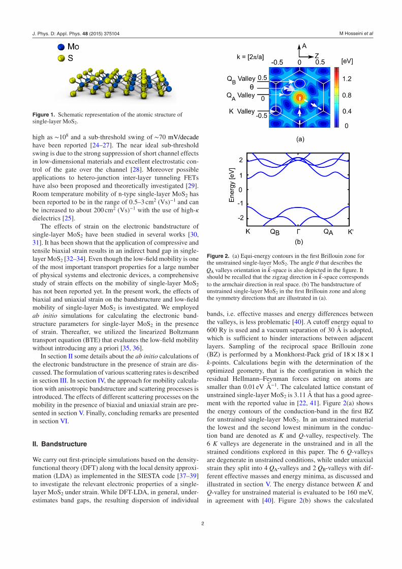
bands, i.e. effective masses and energy differences between the valleys, is less problematic [40]. A cutoff energy equal to 600 Ry is used and a vacuum separation of 30 Å is adopted, which is sufficient to hinder interactions between adjacent layers. Sampling of the reciprocal space Brillouin zone (BZ) is performed by a Monkhorst-Pack grid of × ×18 18 1 k-points. Calculations begin with the determination of the optimized geometry, that is the configuration in which the residual Hellmann–Feynman forces acting on atoms are smaller than 0.01 eV Å−1. The calculated lattice constant of unstrained single-layer MoS2 is 3.11 Å that has a good agree-ment with the reported value in [22, 41]. Figure 2(a) shows the energy contours of the conduction-band in the first BZ for unstrained single-layer MoS2. In an unstrained material the lowest and the second lowest minimum in the conduc-tion band are denoted as K and Q-valley, respectively. The 6 K valleys are degenerate in the unstrained and in all the strained conditions explored in this paper. The 6 Q-valleys are degenerate in unstrained conditions, while under uniaxial strain they split into 4 QA-valleys and 2 QB-valleys with dif-ferent effective masses and energy minima, as discussed and illustrated in section V. The energy distance between K and Q-valley for unstrained material is evaluated to be 160 meV, in agreement with [40]. Figure 2(b) shows the calculated
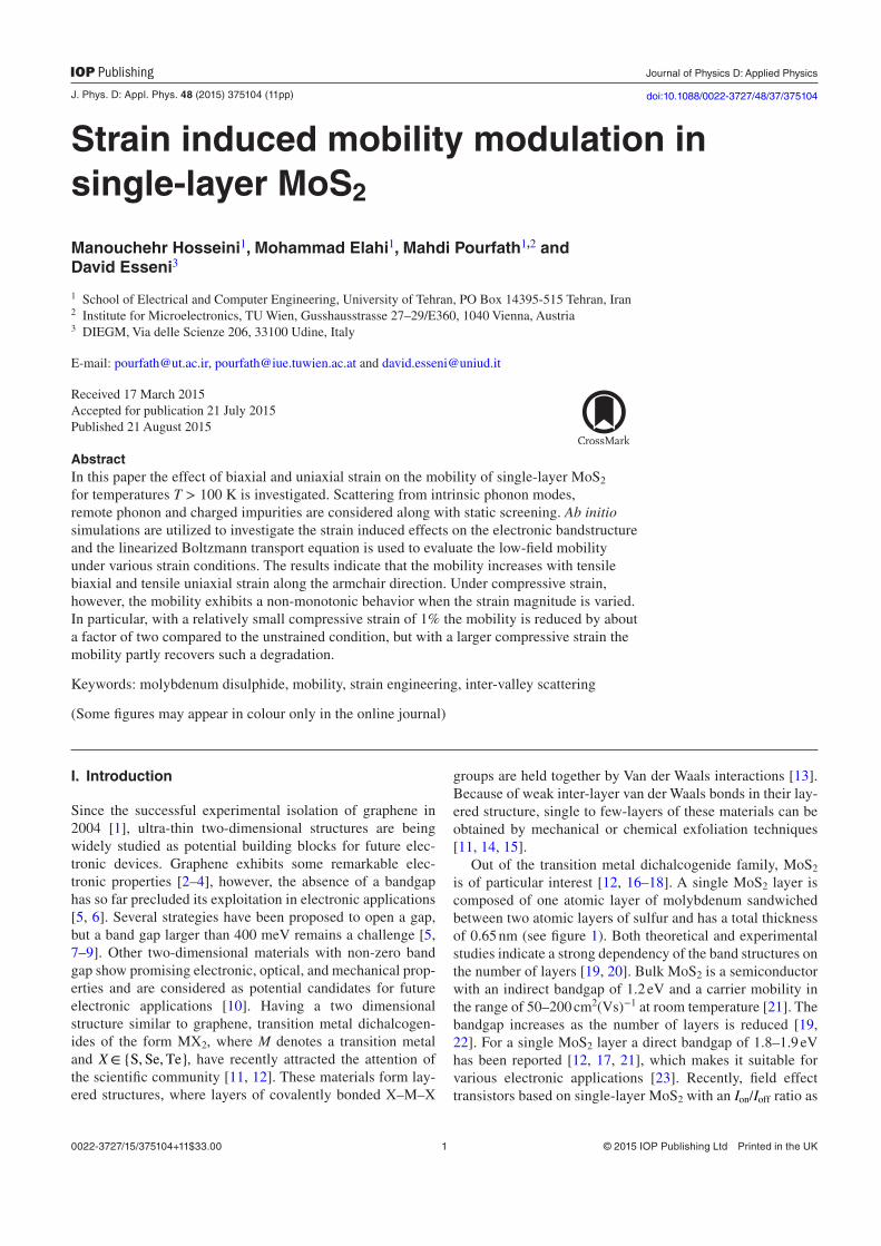
Figure 1. Schematic representation of the atomic structure of single-layer MoS2.
Figure 2. (a) Equi-energy contours in the first Brillouin zone for the unstrained single-layer MoS2. The angle θ that describes the QA valleys orientation in
→k-space is also depicted in the figure. It
should be recalled that the zigzag direction in →k-space corresponds
to the armchair direction in real space. (b) The bandstructure of unstrained single-layer MoS2 in the first Brillouin zone and along the symmetry directions that are illustrated in (a).
J. Phys. D: Appl. Phys. 48 (2015) 375104
M Hosseini et al
3
DFT-LDA band structure and depicts a direct band gap of 1.92 eV at the K-point which is very close to the experimen-tally measured value of 1.85 eV [17].
III. Scattering rates
In this section the formulation of scattering with intrinsic phonon, charged impurities, remote phonon, and the screening effects are presented.
III.A. Scattering with MoS2 phonon modes
Scattering rates due to intrinsic phonons (including acoustic, optical and polar-optical phonons), to remote phonons and to charged impurities are taken into account. Piezoelectric cou-pling to the acoustic phonons is only important at low tem-peratures and is neglected in this work [42]. If the surrounding dielectric provides a large energy barrier for confining elec-trons in the MoS2 layer, the envelope function of mobile elec-
trons can be approximated as χΨ ( ) = ( ) ( )→ → → →r z z k r S, exp i . /k with χ π( ) = ( ) ( )z a z a2/ sin / [43], where S is the area nor-malization factor,
→k is the in-plane two-dimensional wave
vector, a is the thickness of single-layer MoS2 and →r is the in-plane position vector. The scattering rates for the acoustic and optical phonon are discussed first.
Using Fermi’s golden rule the scattering rate from an ini-tial state
→k in valley v to the final state ′
→k in valley w can be
written as
π δ ω( ) =ℏ
∣ ( )∣ [ ( ) − ( ) ∓ ℏ ( )]′ ′ ′→ → → → → →
S k k M k k E k E k q,2
, ,v w v w w v, , 2
(1)
where ∣ ( )∣′→ →
M k k,v w, is the matrix element for the mentioned transition and ωℏ ( )q is the phonon energy that may depend
on = ∣ − ∣′→ →
q k k . The intra-valley transitions (v = w) assisted by acoustic phonons can be approximated as elastic and the rate is given by
πρ
δ( ) =ℏ
[ ( ) − ( )]′ ′→ → → →
S k kk TD
S vE k E k,
2,
sac
B ac2
2 (2)
where kB is the Boltzmann constant, T is the absolute tem-perature, Dac is the acoustic the deformation potential, ρ = × −3.1 10 7 [gr cm−2] is the mass density and vs is the sound velocity of single-layer MoS2. On the other hand, the rate of inelastic phonon scattering, including intra and inter-valley optical phonons, and inter-valley acoustic phonons, can be expressed as
⎡⎣⎢
⎤⎦⎥
πω ρ
δ
ω
( ) =( )
+ ∓ [ ( ) − ( )
∓ ℏ ( )]
′ ′→ → → →
S k kD
Sn E k E k
q
,1
2
1
2
,
v wv w
w vac/op
, ac/op, 2
ac/opop
ac/op (3)
where Dv wac/op, is the acoustic/optical deformation potential
for a transition between valleys v and w, ωℏ ( )qac/op is the phonon energy, and nop is the phonon occupation (upper and
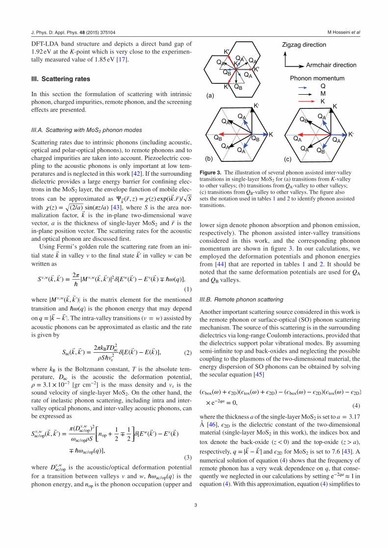
lower sign denote phonon absorption and phonon emission, respectively). The phonon assisted inter-valley transitions considered in this work, and the corresponding phonon momentum are shown in figure 3. In our calculations, we employed the deformation potentials and phonon energies from [44] that are reported in tables 1 and 2. It should be noted that the same deformation potentials are used for QA and QB valleys.
III.B. Remote phonon scattering
Another important scattering source considered in this work is the remote phonon or surface-optical (SO) phonon scattering mechanism. The source of this scattering is in the surrounding dielectrics via long-range Coulomb interactions, provided that the dielectrics support polar vibrational modes. By assuming semi-infinite top and back-oxides and neglecting the possible coupling to the plasmons of the two-dimensional material, the energy dispersion of SO phonons can be obtained by solving the secular equation [45]
ϵ ω ϵ ϵ ω ϵ ϵ ω ϵ ϵ ω ϵ( ( ) + )( ( ) + ) − ( ( ) − )( ( ) − )
× =−e 0,qa
box 2D tox 2D box 2D tox 2D
2
(4)
where the thickness a of the single-layer MoS2 is set to a = 3.17 Å [46], ϵ2D is the dielectric constant of the two-dimensional material (single-layer MoS2 in this work), the indices box and
tox denote the back-oxide (z < 0) and the top-oxide (z > a),
respectively, = ∣ − ∣′→ →
q k k and ϵ2D for MoS2 is set to 7.6 [43]. A numerical solution of equation (4) shows that the frequency of remote phonon has a very weak dependence on q, that conse-quently we neglected in our calculations by setting ≈−e 1qa2 in equation (4). With this approximation, equation (4) simplifies to
Figure 3. The illustration of several phonon assisted inter-valley transitions in single-layer MoS2 for (a) transitions from K-valley to other valleys; (b) transitions from QA-valley to other valleys; (c) transitions from QB-valley to other valleys. The figure also sets the notation used in tables 1 and 2 to identify phonon assisted transitions.
J. Phys. D: Appl. Phys. 48 (2015) 375104

M Hosseini et al
4
ϵ ω ϵ ω( ) + ( ) = 0box tox , that we solved by using the single polar phonon expression for the ϵ ω( )ox in each oxide:
ϵ ω ϵ ϵ ϵω ω
( ) = + −−
∞∞
1 /,ox
0
2TO2 (5)
where ϵ∞ and ϵ0 are the high and low frequency dielectric con-stants, respectively, and ωTO is the frequency of the polar phonon in the oxide. We could provide analytical solution for equation
(5) and express ωso,box as: ( )ω = − + − ( )B B AC A4 / 2so,box2 2
and for ωso,tox as ( )ω = − − − ( )B B AC A4 / 2so,tox2 2 , where
ϵ ϵ= ( + )∞ ∞A tox box , ϵ ϵ ω ϵ ϵ= −( + ) × − ( + ) ×∞ ∞B tox0
box TO,tox2
box0
tox
ωTO,box2 and ϵ ϵ ω ω= ( + ) × ×C tox
0box0
TO,tox2
TO,box2 . Table 3
reports the parameters of dielectric materials that are studied in this work and indicates the corresponding calculated SO phonon frequencies. The scattering matrix element of remote phonon can be written as [45]:
Table 1. Deformation potentials for inelastic phonon assisted transitions in single-layer MoS2.
Phonon momentum
Electron transition
Deformation potential
Γ →K K =D 4.5ac eV
Γ →K K = ×D 5.8 10op8 eV cm−1
K →K K ′ = ×D 1.4 10ac8 eV cm−1
K →K K ′ = ×D 2.0 10op8 eV cm−1
Q →K Q = ×D 9.3 10ac7 eV cm−1
Q →K Q = ×D 1.9 10op8 eV cm−1
M →K Q = ×D 4.4 10ac8 eV cm−1
M →K Q = ×D 5.6 10op8 eV cm−1
Γ →Q Q =D 2.8ac eV
Γ →Q Q = ×D 7.1 10op8 eV cm−1
Q →Q Q = ×D 2.1 10ac8 eV cm−1
Q →Q Q = ×D 4.8 10op8 eV cm−1
M →Q Q = ×D 2.0 10ac8 eV cm−1
M →Q Q = ×D 4.0 10op8 eV cm−1
K →Q Q = ×D 4.8 10ac8 eV cm−1
K →Q Q = ×D 6.5 10op8 eV cm−1
Q →Q K or ′K = ×D 1.5 10ac8 eV cm−1
Q →Q K or ′K = ×D 2.4 10op8 eV cm−1
M →Q K or ′K = ×D 4.4 10ac8 eV cm−1
M →Q K or ′K = ×D 6.6 10op8 eV cm−1
Note: All parameters are taken from [44].
Table 2. The phonon energy for intra-valley and inter-valley transitions at the K, M, and Q points of single-layer MoS2 as reported in [44].
Phonon mode Γ K M Q
Acoustic [meV] 0 26.1 24.2 20.7Optical [meV] 49.5 46.8 47.5 48.1
Note: As discussed in [44], the energy values for acoustic (optical) phonon modes are the average of phonon energies of transverse and longitudinal (transverse, longitudinal and homo-polar) modes.
⎛
⎝⎜⎜
⎞
⎠⎟⎟
ωϵ ϵ ω ϵ ϵ ω
( ) =
ℏ+ ( )
−+ ( )
′
∞
→ →M k k
Sq
,
2
1 1,
so,tox
so,tox
tox box so,tox tox0
box so,tox
(6)
⎛
⎝⎜⎜
⎞
⎠⎟⎟
ωϵ ϵ ω ϵ ϵ ω
( ) =
ℏ+ ( )
−+ ( )
′
∞
→ →M k k
Sq
,
2
1 1,
so,box
so,box
box tox so,box box0
tox so,box
(7)
scattering with SO phonon mode is inelastic and we consider only intra-valley transitions. The corresponding transition rate is
⎡⎣⎢
⎤⎦⎥
π δ
ω
( ) =ℏ
∣ ( )∣ + ∓ [ ( ) − ( )
∓ ℏ ]
′ ′ ′→ → → → → →S k k M k k n E k E k,
2,
1
2
1
2
,
so so2
so
so (8)
where nso and ωℏ so are the SO phonon occupation number and energy, respectively.
III.C. Scattering with coulomb centers
To investigate the effect of the dielectric environment on the scattering of carriers from charged impurities located inside the single-layer MoS2, we assume that the charged impuri-ties are located in the center of the single-layer MoS2 thick-ness, that is at z = a/2. The Fourier transform of the scattering potential due to a charged impurity located at ( ) = ( )→r z a, 0, /2 can be written as [47]
ϕϵ
( ) = [ + + ]− ∣ − ∣ −q zq
C D,e
2e e e ,q z a qz qz
2
2D
/2 (9)
where e is the elementary charge, and C and D can be written as
ϵ ϵ ϵ ϵ ϵ ϵ ϵ ϵ ϵ ϵ ϵ ϵϵ ϵ ϵ ϵ ϵ ϵ ϵ ϵ
=( − )( − ) + ( + )( − ) − ( − )( + )
( + )( + ) − ( − )( − )
−C
e e
e,
qa aq
aq
2D box0
2D tox0 /2
2D box0
2D tox0 /2
box0
2D tox0
2D
2D box0
2D tox0 2
2D box0
2D tox0
(10)
J. Phys. D: Appl. Phys. 48 (2015) 375104

M Hosseini et al
5
and
ϵ ϵϵ ϵ
=( − )[ + ]
+
−D
C e.
qabox0
2D/2
box0
2D (11)
Using equation (9), the χ( )z form χ π( ) = ( ) ( )z a z a2/ sin / and assuming intra-valley transitions for scattering with charged impurities, the transition matrix elements take the form
⎛⎝⎜
⎞⎠⎟
⎡⎣⎢
⎤⎦⎥
⎛⎝⎜
⎞⎠⎟
ϵ π
ϵ π
( ) = −+ ( )
× ( − )+ ( − )−
+ ++ ( )
′( )
− −
→ →M k k
e
qa q
q
q a
C D
e
qa q
q
q a
,1
2 /
2e 1
21 e e
1
2 /,
qa qa qa
cb0
2
2D2 2
/2
2
2D2 2
(12)
where = ∣ − ∣′→ →
q k k . Equation (12) expresses the matrix element for a Coulomb center located in ( ) = ( )→r z a, 0, /2 and does not account for the screening produced by the free carriers in MoS2; such a screening effect is introduced according to the dielectric matrix approach discussed in section III.D. The overall matrix element produced by a set of Coulomb cen-ters randomly distributed at positions ( )→r a, /2 is known to be affected by the statistical properties of the distribution and, in particular, by a possible correlation between the position of Coulomb centers. In this paper we do not address these difficulties and simply write the overall matrix element as ∣ ( )∣ = [ ∣ ( )∣ ]′ ′( )→ → → →M k k N M k k S, , /cb
2D cb
0 2 , where ND is the impu-rity density per unit area and ( )Mcb
0 is given by equation (12). Scattering charged impurities is treated as elastic and the rate is therefore given by
π δ( ) =ℏ
∣ ( )∣ ( ( ) − ( ))′ ′ ′→ → → → → →S k k M k k E k E k,
2, .cb cb
2 (13)
III.D. Screening
The effect of static screening produced by the electrons in the MoS2 conduction band is described by using the dielectric function approach [47], so that the screened matrix element
( )′→ →
M k k,wscr of the valley w is obtained by solving the linear
problem:
∑ ϵ( ) = ( ) ( )M q q M q ,v
w
v w w,scr (14)
where Mv(q) are the unscreened matrix element. As can be seen in figure 2(a), there are three different valleys in strained single-layer MoS2 (K, QA and QB valleys), hence v,
∈ { }w K Q Q, ,A B . In equation (14), ϵv w, is the dielectric matrix which is introduced as:
ϵ δϵ ϵ
( ) = −( + )
Π ( ) ( )qe
qq F q ,v w
v ww v w,
,
2
2D box
, (15)
where δv w, is the Kronecker symbol (1 if v = w, otherwise zero), Π ( )qw and Fv,w(q) are the polarization factor and unit-less screening form factor, respectively [47]. In the case at study the dielectric matrix can be analytically inverted to eval-uate screened matrix elements as:
⎛
⎝⎜
⎞
⎠⎟ϵ ϵ
ϵ( ) =
− ∑ ( ) ( ) + ∑ ( ) ( )
− ∑ ( )≠ ≠
M q
q M q q M q
q
1
2.v w v
v w v
w v
v w w
w
v wscr
, ,
, (16)
The static dielectric function approach described above has been directly used for the scattering due to charged impurities, while the situation is admittedly more complicated for phonon scattering. For the inelastic, inter-valley phonon transitions described in tables 1 and 2 the relatively large phonon wave-vector (see also figure 3) and the non-null phonon energies suggest that it is safe to leave these transitions unscreened, because the dynamic descreening and the large phonon wave-vectors make the screening very ineffective. Arguments con-cerning screening for intra-valley acoustic phonons are more subtle and controversial and a thorough discussion for inver-sion layer systems can be found in [48]. We here decided to leave also intra-valley acoustic phonons unscreened, which is the choice employed in essentially all the studies concerning transport in inversion layers that the authors are aware of. The screening of the SO phonon scattering is also a delicate sub-ject, because the polar phonon modes of the high-κ dielectrics can couple with the collective excitations of the electrons in the MoS2 layer and thus produce coupled phonon-plasmon modes [45, 48], whose treatment is further complicated by the possible occurrence of Landau damping [45, 48, 49]. In this paper we do not attempt a full treatment of the coupled phonon-plasmon modes [45, 48], but instead show in in sec-tion V results for the two extreme cases of either unscreened SO phonons or SO phonons screened according to the static dielectric function. We can anticipate that while the inclu-sion of static screening in SO phonons implies a significant mobility enhancement compared to the unscreened case, the
Table 3. Parameters for the top-oxide dielectric materials taken from (a) [52] and (b) [53] and corresponding calculated SO phonon frequencies ωℏ so,tox and ωℏ so,box.
Material ( )SiO2a BN(b) AlN(a) ( )Al O2 3
a ( )HfO2a ( )ZrO2
a
ϵtox0 3.9 5.09 9.14 12.53 23 24
ϵ∞tox 2.5 4.1 4.8 3.2 5.03 4
ωTO,tox [meV] 55.6 93.07 81.4 48.18 12.4 16.67ωso,tox [meV] (Evaluated in this work) 69.4 100.5 104.3 83.9 21.3 30.5ωso,box [meV] (Evaluated in this work) 69.4 60.1 58.0 54.2 61.1 62.9
Note: In all of the cases back-oxide is assumed to be SiO2.
J. Phys. D: Appl. Phys. 48 (2015) 375104
M Hosseini et al
6
mobility dependence on the strain and on the dielectric con-stant of the high-κ dielectrics is not significantly affected by the treatment of screening for SO phonons.
IV. Mobility calculation
Acoustic, optical, polar-optical, remote phonon, and charged impurity scatterings are considered for the calculation of low-field mobility. As it will be discussed in the next section, the bandstructure for QA and QB valleys is not isotropic and the mobility shows direction-dependence, hence we calculated mobility by solving numerically the linearized Boltzmann transport equation (BTE) according to the approach described in [35], which does not introduce any simplifying assump-tion in the BTE solution. In particular, mobility has been cal-culated along the armchair and zigzag directions and strain has been also studied for the uniaxial configuration along either armchair or zigzag direction, as well as for the biaxial configuration.
In order to describe in more detail the mobility calcula-tion procedure, we first recall that the longitudinal direction of QA-valley is neither the armchair nor the zigzag direc-tion, and figure 2(a) shows that θ is the angle describing the valley orientation with respect to the zigzag direction in k-space (i.l. armchair direction in real space). Let us
now consider first the case of the mobility μ( )vA of valley v
along the armchair direction, that can be written by defini-tion as μ =( ) ( )J F/v v
A A A, where ( )J vA is the current component in
the armchair direction for the valley v induced by the elec-tric field FA along armchair direction. The current ( )J v
A can be expressed as θ θ= ( ) + ( )( ) ( ) ( )J J Jcos sinv
lv
v tv
vA in terms of the current components ( )Jl
v , ( )Jtv along, respectively, the longitu-
dinal and transverse direction of the valley v. By denoting the longitudinal (Fl) and transverse component (Ft) of the elec-tric field as θ= ( )F F cosl vA and θ= ( )F F sint vA , the currents
( )Jlv and ( )Jt
v in turn can be written as μ μ= +( ) ( ) ( )J F Flv
llv
l ltv
t and μ μ= +( ) ( ) ( )J F Ft
vltv
l ttv
t, where μll, μtt and μlt are the entries of the two by two mobility matrix in the valley coordinate system [47]. Consequently we finally obtain:
μ μ θ μ θ μ θ θ= = ( ) + ( ) + ( ) ( )( )( )
( ) ( ) ( )J
Fcos sin 2 sin cos .v
v
llv
v ttv
v ltv
v vAA
A
2 2
(17)
By following a similar procedure, the mobility μ( )vZ of the
valley v along the zigzag direction can be written as:
μ μ θ μ θ μ θ θ= = ( )+ ( )− ( ) ( )( )( )
( ) ( ) ( )J
Fsin cos 2 sin cos .v
v
llv
v ttv
v ltv
v vZZ
Z
2 2
(18)For the circular and elliptical bands employed in our
calculations (see figure 4(g)), μ( )ltv is zero for symmetry rea-
sons [47]. After calculating the mobility for each valley, the overall mobilities μA and μZ are obtained as the average of the mobility in the different valleys weighted by the corre-sponding electron density.
Equations (17) and (18) allow us to calculate the mobility
μ( )vA and μ( )v
Z from the longitudinal μllv and the transverse
mobility μttv of the valley v which are the mobilities obtained
from the linearized BTE when the electric field is either in the longitudinal or in the transverse direction of the valley v. As already said, the μll
v and μttv have been obtained by using the
approach of [35], whose derivation for the case at study in this work can be summarized as follows. The out of equilibrium occupation function ( )
→f kv for the valley v in the presence of a
field Fx is written as
( ) = ( ( )) − ( )→ → →
f k f E k eF g k ,v vx
v0 (19)
where f 0(E) is the equilibrium Fermi–Dirac distribution function, ∈ { }x l t, is either the longitudinal or the transverse direction of the valley and = ( )
→k k k,l t is the wavevector in
the valley coordinate system. Equation (19) is a definition of ( )
→g kv , which is the unknown function of the linearized BTE problem. For a two-dimensional system the linearized BTE can be written as [35]
⎛
⎝⎜⎜
⎞
⎠⎟⎟∫
∫
∑
∑
πδ ω
πδ ω
( )ℏ
Γ ( ) [ ( ) − ( ) ∓ ℏ ]
−ℏ
Λ ( ) ( ) [ ( ) − ( ) ∓ ℏ ]
= ( )( ( ( )))( − ( ( )))
′ ′ ′
′ ′ ′ ′
→
→
′
′
→ → → → → →
→ → → → → →
→→ →
g k k k E k E k k
k k g k E k E k k
v kf E k f E k
k T
1
2, d
1
2, d
1,
v
wk
v w w vph
w k
v w w w v
xv
v v
,
,
0 0
B
(20)
where vxv is the x component of the group velocity of valley
v and, for convenience of notation, we have introduced the quantities
⎡
⎣⎢⎢
⎤
⎦⎥⎥
⎡
⎣⎢⎢
⎤
⎦⎥⎥
Γ ( ) = ∣ ( )∣− ( ( ))− ( ( ))
Λ ( ) = ∣ ( )∣( ( ))( ( ))
′ ′′
′ ′′
⎯→ → ⎯→ →→
⎯→
⎯→ → ⎯→ →⎯→
→
k k M k kf E k
f E k
k k M k kf E k
f E k
, ,1
1
, ,
v w v ww
v
v w v wv
w
, , 2 0
0
, , 2 0
0
(21)
To numerically solve equation (20), we employed the discretization scheme introduced in [35]:
→k is discretized
according to a uniform angular step βΔ and also a uniform energy step. The discrete values kv, r, d of the wave-vector mag-nitude correspond to one of the discrete energy values and the generic discrete wave-vector β= ( Δ )
→k k d,v r d v r d, , , , is identified
by the magnitude kv, r, d and the angle βΔd (with d being a positive integer number). For each scattering mechanism, by converting the integral over
→k in an integral over the energy
and the angle β and then using the above mentioned discre-tization, equation (20) can be rewritten as:
⎡
⎣⎢⎢
⎤
⎦⎥⎥∑ ∑β
πδ β
πδ( ) Δ
ℏ− Δ
ℏ( )
=( ) ( ( ))[ − ( ( ))]
′ ′
′ ′ ′ ′
′ ′
′ ′′ ′
′ ′g k A B g k
v k f E k f E k
k T
2 2
1.
v r d
w r dv r dw r d
v r dw r d
w r dv r dw r d
w r d v r dw r d
x v r d v r d v r d
, ,
, ,, ,, ,
, ,, ,
, ,, ,, ,
, , , ,, ,
, , 0 , , 0 , ,
B
(22)
Equation (22) is a linear problem for the discretized unknown values g(kv, r, d) written in terms of the coefficients
′ ′Av r dw r d, ,, , and ′ ′Bv r d
w r d, ,, , defined as
J. Phys. D: Appl. Phys. 48 (2015) 375104
M Hosseini et al
7
⎡
⎣
⎢⎢⎢
⎤
⎦
⎥⎥⎥( )=
× ∣ ( )∣ − ( ( ))− ( ( ))( )′ ′
′ ′ ′ ′ ′ ′ ′ ′A
k M k k f E k
f E k
, 1
1,v r d
w r d w r dv w
v r d w r d
E k
k
w r d
v r d, ,, , , ,
,, , , ,
2
d
d
0 , ,
0 , ,w r d, ,
(23)
⎡
⎣⎢
⎤
⎦⎥( )=
× ∣ ( )∣ ( ( ))( ( ))( )′ ′
′ ′ ′ ′ ′ ′
′ ′B
k M k k f E k
f E k
,,v r d
w r d w r dv w
v r d w r d
E k
k
v r d
w r d, ,, , , ,
,, , , ,
2
d
d
0 , ,
0 , ,w r d, ,
(24)where the non-zero entries of the matrix representing the
linear problem are governed by the Kronecker symbols δ ′ ′v r dw r d, ,, , ,
that are defined so to enforce energy conservation [35].Equation (22) has been written for a single scattering
mechanism. In order to accommodate several scattering mechanisms in our calculations, we do not resort to an approximated treatment based on the Matthiessen rule [50], but instead follow [35] and notice that equation (22) can be
written in the concise matrix notation =( )M g G
s, where
( )M
s
is a matrix specific of the scattering mechanisms s, g is the unknown vector and G is the vector at the right hand side of equation (22) and consisting of known quantities. Hence the unknown vector g corresponding to several scattering mecha-nisms can be obtained by solving the linear problem
∑ ==
( )⎡
⎣⎢⎢
⎤
⎦⎥⎥
M g G,s
Ns
1
SC
(25)
where equation (22)–(24) will totally define the entries of the matrix
( )M
s for each scattering mechanism.
V. Results and discussions
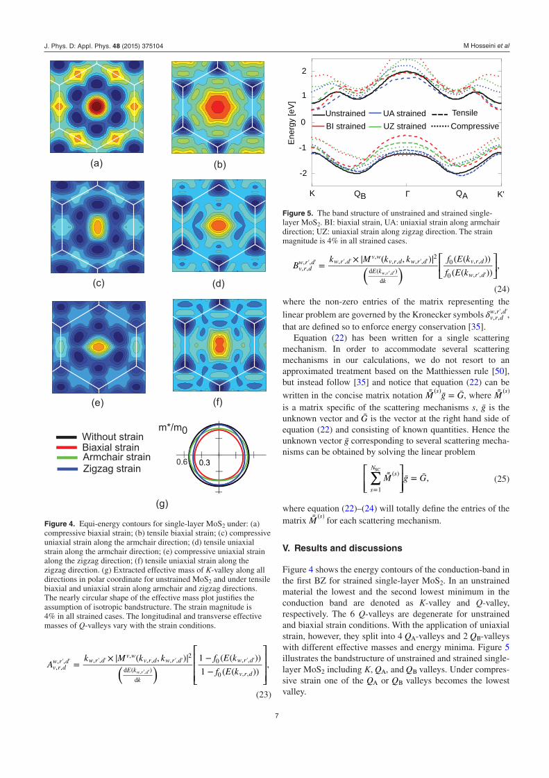
Figure 4 shows the energy contours of the conduction-band in the first BZ for strained single-layer MoS2. In an unstrained material the lowest and the second lowest minimum in the conduction band are denoted as K-valley and Q-valley, respectively. The 6 Q-valleys are degenerate for unstrained and biaxial strain conditions. With the application of uniaxial strain, however, they split into 4 QA-valleys and 2 QB-valleys with different effective masses and energy minima. Figure 5 illustrates the bandstructure of unstrained and strained single-layer MoS2 including K, QA, and QB valleys. Under compres-sive strain one of the QA or QB valleys becomes the lowest valley.
Figure 4. Equi-energy contours for single-layer MoS2 under: (a) compressive biaxial strain; (b) tensile biaxial strain; (c) compressive uniaxial strain along the armchair direction; (d) tensile uniaxial strain along the armchair direction; (e) compressive uniaxial strain along the zigzag direction; (f) tensile uniaxial strain along the zigzag direction. (g) Extracted effective mass of K-valley along all directions in polar coordinate for unstrained MoS2 and under tensile biaxial and uniaxial strain along armchair and zigzag directions. The nearly circular shape of the effective mass plot justifies the assumption of isotropic bandstructure. The strain magnitude is 4% in all strained cases. The longitudinal and transverse effective masses of Q-valleys vary with the strain conditions.
Figure 5. The band structure of unstrained and strained single-layer MoS2. BI: biaxial strain, UA: uniaxial strain along armchair direction; UZ: uniaxial strain along zigzag direction. The strain magnitude is 4% in all strained cases.
J. Phys. D: Appl. Phys. 48 (2015) 375104
M Hosseini et al
8
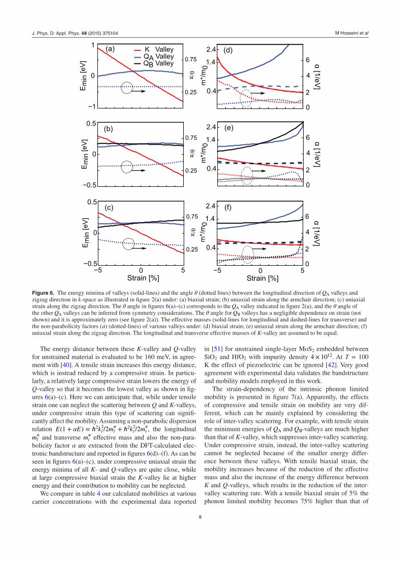
The energy distance between these K-valley and Q-valley for unstrained material is evaluated to be 160 meV, in agree-ment with [40]. A tensile strain increases this energy distance, which is instead reduced by a compressive strain. In particu-larly, a relatively large compressive strain lowers the energy of Q-valley so that it becomes the lowest valley as shown in fig-ures 6(a)–(c). Here we can anticipate that, while under tensile strain one can neglect the scattering between Q and K-valleys, under compressive strain this type of scattering can signifi-cantly affect the mobility. Assuming a non-parabolic dispersion relation α( + ) = ℏ * + ℏ *E E k m k m1 /2 /2l l t t
2 2 2 2 , the longitudinal *ml and transverse *mt effective mass and also the non-para-
bolicity factor α are extracted from the DFT-calculated elec-tronic bandstructure and reported in figures 6(d)–(f). As can be seen in figures 6(a)–(c), under compressive uniaxial strain the energy minima of all K- and Q-valleys are quite close, while at large compressive biaxial strain the K-valley lie at higher energy and their contribution to mobility can be neglected.
We compare in table 4 our calculated mobilities at various carrier concentrations with the experimental data reported
in [51] for unstrained single-layer MoS2 embedded between SiO2 and HfO2 with impurity density ×4 1012. At T = 100 K the effect of piezoelectric can be ignored [42]. Very good agreement with experimental data validates the bandstructure and mobility models employed in this work.
The strain-dependency of the intrinsic phonon limited mobility is presented in figure 7(a). Apparently, the effects of compressive and tensile strain on mobility are very dif-ferent, which can be mainly explained by considering the role of inter-valley scattering. For example, with tensile strain the minimum energies of QA and QB-valleys are much higher than that of K-valley, which suppresses inter-valley scattering. Under compressive strain, instead, the inter-valley scattering cannot be neglected because of the smaller energy differ-ence between these valleys. With tensile biaxial strain, the mobility increases because of the reduction of the effective mass and also the increase of the energy difference between K and Q-valleys, which results in the reduction of the inter-valley scattering rate. With a tensile biaxial strain of 5% the phonon limited mobility becomes 75% higher than that of
Figure 6. The energy minima of valleys (solid-lines) and the angle θ (dotted lines) between the longitudinal direction of QA valleys and zigzag direction in k-space as illustrated in figure 2(a) under: (a) biaxial strain; (b) uniaxial strain along the armchair direction; (c) uniaxial strain along the zigzag direction. The θ angle in figures 6(a)–(c) corresponds to the QA valley indicated in figure 2(a), and the θ angle of the other QA valleys can be inferred from symmetry considerations. The θ angle for QB valleys has a negligible dependence on strain (not shown) and it is approximately zero (see figure 2(a)). The effective masses (solid-lines for longitudinal and dashed-lines for transverse) and the non-parabolicity factors (α) (dotted-lines) of various valleys under: (d) biaxial strain; (e) uniaxial strain along the armchair direction; (f) uniaxial strain along the zigzag direction. The longitudinal and transverse effective masses of K-valley are assumed to be equal.
J. Phys. D: Appl. Phys. 48 (2015) 375104

M Hosseini et al
9
unstrained material. In contrast, a compressive biaxial strain of 0.8% strongly reduces the mobility due to the reduction of energy difference between K and Q-valleys (see figure 6(a)) and increased inter-valley scattering. With further increase of compressive biaxial strain, Q-valleys become the lowest ones and thus dominate the mobility. At a strain value of about 2.5% the contribution of K-valleys to mobility becomes neg-ligible and the mobility behavior is completely determined by the Q-valleys. Longitudinal and transverse effective masses of Q-valleys are not equal and are somewhat changed by strain, however, the different angular dependency of mobility along the armchair and zigzag direction tends to compensate the changes of effective masses and the overall mobility remains nearly constant at larger compressive strain values.
Under tensile uniaxial strain the mobility is hardly affected by a strain along the zigzag direction, while it increases for strain along the armchair direction. In both cases the variation of the effective mass and non-parabolicity factor with strain determine the mobility behavior. Under a compressive uniaxial strain along the armchair direction, QA becomes the lowest valley, while for a strain along the zigzag direction QB is the lowest one. These
results emphasize that the contribution of both QA and QB valley should be included for an accurate calculation of mobility. Under a compressive strain of about 1.5% the mobilities are strongly reduced, but they remain nearly constant for larger strain mag-nitudes. Moreover, we notice that for a strain along the zigzag direction, the mobility along the strain direction becomes slightly larger than the mobility in the armchair direction.
Figure 7(b) reports the mobility in the presence of intrinsic phonon and charged impurity scattering. The top and bottom oxide are assumed to be SiO2 and both carrier and impurity concentrations are 1012 cm−2. Except for a global reduc-tion of the mobility, the behavior of the mobility with strain is similar to figure 7(a) corresponding to the phonon limited mobility. The results presented in figure 7(c) correspond to the same parameters as in figure 7(b), except for a reduction of carrier concentration to 1011 cm−2. As the carrier concentra-tion decreases the effect of static screening becomes weaker and the mobility is further reduced. Figure 7(d) illustrates the mobility as a function of strain with the same parameters used in figure 7(b), expect for the top and bottom gate oxide which is Al2O3. A high-κ dielectric implies a larger dielectric screening
Table 4. The comparison of the calculated mobility (μ) in this work with the experimental data of [51] at various carrier concentrations (n).
Carrier concentration [cm−2] ×7.6 1012 ×9.6 1012 ×1.15 1013 ×1.35 1013
Calculated mobility, this work [cm2 (Vs)−1] 93 106 114 122Experimental mobility [cm2 (Vs)−1] ±96 3 ±111 3 ±128 3 ±132 3
Note: T = 100 K and the impurity density is equal to ×4 1012 cm−2.
Figure 7. (a) The phonon limited mobility of single-layer MoS2 as a function of strain with a carrier concentration n = 1012 cm−2. The mobility limited by phonon and screened charged impurity scattering with SiO2 as the gate oxide (ϵ = 3.9r ) and carrier (n) and charged impurity concentration (nimp) for: (b) = =n n 10imp
12 cm−2; (c) n = 1011 cm−2 and =n 10imp12 cm−2. (d) Same as (b), except for the top-
oxide which is Al2O3. In the legend, BI, UA, and UZ denote a biaxial strain, a uniaxial strain along the armchair direction, and a uniaxial strain along the zigzag direction respectively. The subscripts A and Z indicate the component of the mobility along the armchair or zigzag direction. For example: UZA is the mobility along the armchair direction for a uniaxial strain along zigzag direction.
J. Phys. D: Appl. Phys. 48 (2015) 375104

M Hosseini et al
10
and increases the mobility. Under this condition, with a ten-sile biaxial strain of 5% and a tensile uniaxial strain of 5% along the armchair direction the mobility increases by 53% and 43%, respectively, compared to an unstrained single-layer MoS2. For a better comparison, figure 8 shows the room tem-perature mobility versus carrier concentration and also versus the dielectric constant for the unstrained material and for 5% tensile strain in either a biaxial or a uniaxial configuration along the armchair direction with an impurity density equal to 1012 cm−2. As can be seen in figure 8(a), because of screening the mobility increases with the carrier concentration for both unstrained and strained cases. Figure 8(b) indicates that the strain induced mobility enhancement with high-κ dielectric materials is slightly larger than that with low-κ materials.
The effect of unscreened and screened remote phonon scat-tering on the mobility of unstrained and 5% biaxial strained single-layer MoS2 are compared in figure 9. Except for a global increase of mobility values. The mobility dependence on the dielectric constant κ is not significantly affected by the screening of SO phonons. As can be seen, for relatively
small κ values, mobility improves with increasing κ because of the dielectric screening of charged impurities [43]. At high κ values, however, the mobility decrease with increasing κ because the corresponding smaller SO phonon energies (see table 3) tend to increase momentum relaxation time via SO phonons. For the conditions considered in figure 9 (tempera-ture, carrier and impurity concentrations, and semi-infinite dielectrics with SiO2 as the bottom oxide), AlN appears to be the optimal top dielectric material for strained and also unstrained single-layer MoS2. Figure 10 shows the tempera-ture dependency of the mobility for unstrained and 5% biaxial strain with HfO2 as the top oxide. As expected the effect of inelastic remote phonons increases with temperature for both unstrained and strained cases. Therefore, it is expected that the optimal material as a top dielectric for temperatures above (bellow) 300 K, should have a lower(higher)-κ com-pared to AlN.
VI. Conclusion
A comprehensive theoretical study on the role of strain on the mobility of single-layer MoS2 is presented. DFT calculations
Figure 8. (a) The mobility versus carrier concentration with and without screening for the unstrained MoS2, for a tensile biaxial strain of 5%, and for a uniaxial strain of 5% along the armchair direction. =n 10imp
12 cm−2. (b) The mobility versus the relative dielectric constant for unstrained MoS2 and for strain conditions as in (a). = =n n 10imp
12 cm−2. The strain induced mobility enhancement is shown on the right-side of the y-axis.
Figure 9. The mobility accounting for intrinsic phonon and charged impurity scattering (triangle), and for either unscreened (rectangle) or screened (circle) SO phonon scattering as a function of top oxide dielectric constant for unstrained (blue line) and 5% biaxial strain (red line). Numbers 1–6 indicate the κ value corresponding to dielectric materials studied in this work (see also table 3). In particular, (1): SiO2, (2): BN, (3): AlN, (4): Al2O3, (5): HfO2, and (6): ZrO2. In all cases the back oxide is assumed to be SiO2. T = 300 K, the impurity and carrier concentrations are equal to ×4 1012 cm−2 and 1013 cm−2, respectively. These values are consistent with experimental data reported in [51].
Figure 10. The mobility with the inclusion of intrinsic phonon and charged impurity scattering (dash line) and with the inclusion of screened SO phonon (solid line) versus temperature for a SiO2/MoS2/HfO2 structure for unstrained (blue line) and 5% biaxial strain (red line). The impurity and carrier concentrations are equal to ×4 1012 cm−2 and 1013 cm−2, respectively.
J. Phys. D: Appl. Phys. 48 (2015) 375104
M Hosseini et al
11
are used to obtain the effective masses and energy minima of the contributing valleys. Thereafter, the linearized BTE is solved for evaluating the mobility, including the effect of intrinsic phonons, remote phonons, and screened charged impurities. The results indicate that, a tensile strain increases the mobility, while compressive strain reduces the mobility. Furthermore, biaxial strain and uniaxial strain along the arm-chair direction increase the mobility more effectively. The strain-dependency of the mobility of MoS2 is rather com-plicated and strongly depends on the relative positions of Q and K-valleys and the corresponding inter-valley scattering. The presented results pave the way for a possible strain engi-neering of the electronic transport in MoS2 based electron devices and the awareness of the quite critical mobility depen-dence on strain may also prove useful in the interpretation of the electron mobility experimental data in single-layer MoS2 transistors.
Acknowledgments
This work has been partly supported by Iran National Science Foundation (INSF).
References
[1] Novoselov K S, Geim A K, Morozov S, Jiang D, Zhang Y, Dubonos S, Grigorieva I and Firsov A 2004 Science 306 666–9
[2] Lin Y M, Dimitrakopoulos C, Jenkins K A, Farmer D B, Chiu H Y, Grill A and Avouris P 2010 Science 327 662
[3] Wang H W H, Nezich D, Kong J K J and Palacios T 2009 IEEE Electron Device Lett. 30 547–9
[4] Dean C et al 2010 Nat. Nanotechnol. 5 722–6 [5] Zhang Y, Tang T T, Girit C, Hao Z, Martin M C, Zettl A,
Crommie M F, Shen Y R and Wang F 2009 Nature 459 820–3 [6] Gava P, Lazzeri M, Saitta A M and Mauri F 2009 Phys. Rev. B
79 165431 [7] Son Y W, Cohen M L and Louie S G 2006 Phy. Rev. Lett.
97 216803 [8] Giovannetti G, Khomyakov P A, Brocks G, Kelly P J and van
den Brink J 2007 Phys. Rev. B 76 073103 [9] Han M Y, Özyilmaz B, Zhang Y and Kim P 2007 Phys. Rev.
Lett. 98 206805 [10] Neto A and Novoselov K 2011 Rep. Prog. Phys. 74 82501–9 [11] Novoselov K, Jiang D, Schedin F, Booth T, Khotkevich V,
Morozov S and Geim A 2005 Proc. Natl Acad. Sci. 102 10451–3
[12] Mak K F, Lee C, Hone J, Shan J and Heinz T F 2010 Phys. Rev. Lett. 105 136805
[13] Wilson J and Yoffe A 1969 Adv. Phys. 18 193–335 [14] Ayari A, Cobas E, Ogundadegbe O and Fuhrer M S 2007 J.
Appl. Phys. 101 014507 [15] Matte H R, Gomathi A, Manna A K, Late D J, Datta R,
Pati S K and Rao C 2010 Angew. Chem. Int. Ed. 122 4153–6
[16] Korn T, Heydrich S, Hirmer M, Schmutzler J and Schüller C 2011 Appl. Phys. Lett. 99 102109
[17] Splendiani A, Sun L, Zhang Y, Li T, Kim J, Chim C Y, Galli G and Wang F 2010 Nano Lett. 10 1271–5
[18] Mak K F, He K, Lee C, Lee G H, Hone J, Heinz T F and Shan J 2013 Nat. Mater. 12 207–11
[19] Kumar A and Ahluwalia P 2012 Eur. J. Phys. B 85 1–7 [20] Zhang L and Zunger A 2015 Nano Lett. 15 949–57 [21] Yun W S, Han S W, Hong S C, Kim I G and Lee J D 2012
Phys. Rev. B 85 033305 [22] Chang C H, Fan X, Lin S H and Kuo J L 2013 Phys. Rev. B
88 195420 [23] Yoon Y, Ganapathi K and Salahuddin S 2011 Nano Lett.
11 3768–73 [24] Radisavljevic B, Whitwick M B and Kis A 2011 ACS Nano
5 9934–8 [25] Radisavljevic B, Radenovic A, Brivio J, Giacometti V and
Kis A 2011 Nat. Nanotechol. 6 147–50 [26] Wang H, Yu L, Lee Y H, Shi Y, Hsu A, Chin M L, Li L J,
Dubey M, Kong J and Palacios T 2012 Nano Lett. 12 4674–80
[27] Kim S et al 2012 Nat. Commun. 3 1011 [28] Schwierz F 2010 Nat. Nanotechnol. 5 487–96 [29] Li M O, Esseni D, Snider G, Jena D and Xing H G 2014 J.
Appl. Phys. 115 074508 [30] Shi H, Pan H, Zhang Y W and Yakobson B I 2013 Phys. Rev.
B 87 155304 [31] Conley H J, Wang B, Ziegler J I, Haglund R F Jr,
Pantelides S T and Bolotin K I 2013 Nano Lett. 13 3626–30 [32] Tabatabaei S M, Noei M, Khaliji K, Pourfath M and
Fathipour M 2013 J. Appl. Phys. 113 163708 [33] Feng J, Qian X, Huang C W and Li J 2012 Nat. Photonics
6 866–72 [34] Ghorbani-Asl M, Borini S, Kuc A and Heine T 2013 Phys.
Rev. B 87 235434 [35] Paussa A and Esseni D 2013 J. Appl. Phys. 113 093702 [36] Fletcher K and Butcher P 1972 J. Phys. C: Solid State 5 212 [37] Soler J M, Artacho E, Gale J D, Garc A, Junquera J, Ordejón P
and Sánchez-Portal D 2002 J. Phys.: Condens. Matter 14 2745
[38] Han S et al 2011 Phys. Rev. B 84 045409 [39] Lebegue S and Eriksson O 2009 Phys. Rev. B 79 115409 [40] Kaasbjerg K, Thygesen K S and Jacobsen K W 2012 Phys.
Rev. B 85 115317 [41] Ataca C and Ciraci S 2011 J. Phys. Chem. C
115 13303–11 [42] Kaasbjerg K, Thygesen K S and Jauho A P 2013 Phys. Rev. B
87 235312 [43] Ma N and Jena D 2014 Phys. Rev. X 4 011043 [44] Li X, Mullen J T, Jin Z, Borysenko K M, Nardelli M B and
Kim K W 2013 Phys. Rev. B 87 115418 [45] Ong Z Y and Fischetti M V 2013 Phys. Rev. B 88 045405 [46] Yue Q, Kang J, Shao Z, Zhang X, Chang S, Wang G, Qin S
and Li J 2012 Phys. Lett. A 376 1166–70 [47] Esseni D, Palestri P and Selmi L 2011 Nanoscale MOS
Transistors (Cambridge: Cambridge University Press) [48] Fischetti M V and Laux S E 1993 Phys. Rev. B
48 2244 [49] Toniutti P, Palestri P, Esseni D, Driussi F, De Michielis M and
Selmi L 2012 J. Appl. Phys. 112 034502 [50] Esseni D and Driussi F 2011 IEEE Tran. Electron Devices
58 2415–22 [51] Radisavljevic B and Kis A 2013 Nat. Mater. 12 815–20 [52] Konar A, Fang T and Jena D 2010 Phys. Rev. B 82 115452 [53] Perebeinos V and Avouris P 2010 Phys. Rev. B 81 195442
J. Phys. D: Appl. Phys. 48 (2015) 375104