stratix device handbook, volume 1 (3 mb)
TRANSCRIPT

101 Innovation DriveSan Jose, CA 95134(408) 544-7000http://www.altera.com
Stratix Device Handbook, Volume 1
S5V1-3.4

Copyright © 2006 Altera Corporation. All rights reserved. Altera, The Programmable Solutions Company, the stylized Altera logo, specific device des-ignations, and all other words and logos that are identified as trademarks and/or service marks are, unless noted otherwise, the trademarks andservice marks of Altera Corporation in the U.S. and other countries. All other product or service names are the property of their respective holders. Al-tera products are protected under numerous U.S. and foreign patents and pending applications, maskwork rights, and copyrights. Altera warrantsperformance of its semiconductor products to current specifications in accordance with Altera's standard warranty, but reserves the right to makechanges to any products and services at any time without notice. Altera assumes no responsibility or liability arising out of the ap-plication or use of any information, product, or service described herein except as expressly agreed to in writing by AlteraCorporation. Altera customers are advised to obtain the latest version of device specifications before relying on any published in-formation and before placing orders for products or services.
ii Altera Corporation

Altera Corporation iii
Contents
Chapter Revision Dates .......................................................................... vii
About This Handbook .............................................................................. ixHow to Find Information ........................................................................................................................ ixHow to Contact Altera ............................................................................................................................. ixTypographic Conventions ........................................................................................................................ x
Section I. Stratix Device Family Data SheetRevision History ............................................................................................................................ Part I–1
Chapter 1. IntroductionIntroduction ............................................................................................................................................ 1–1Features ................................................................................................................................................... 1–2
Chapter 2. Stratix ArchitectureFunctional Description .......................................................................................................................... 2–1Logic Array Blocks ................................................................................................................................ 2–3
LAB Interconnects ............................................................................................................................ 2–4LAB Control Signals ......................................................................................................................... 2–5
Logic Elements ....................................................................................................................................... 2–6LUT Chain & Register Chain .......................................................................................................... 2–8addnsub Signal ................................................................................................................................. 2–8LE Operating Modes ........................................................................................................................ 2–8Clear & Preset Logic Control ........................................................................................................ 2–13
MultiTrack Interconnect ..................................................................................................................... 2–14TriMatrix Memory ............................................................................................................................... 2–21
Memory Modes ............................................................................................................................... 2–22Clear Signals .................................................................................................................................... 2–24Parity Bit Support ........................................................................................................................... 2–24Shift Register Support .................................................................................................................... 2–25Memory Block Size ......................................................................................................................... 2–26Independent Clock Mode .............................................................................................................. 2–44Input/Output Clock Mode ........................................................................................................... 2–46Read/Write Clock Mode ............................................................................................................... 2–49Single-Port Mode ............................................................................................................................ 2–51Multiplier Block .............................................................................................................................. 2–57Adder/Output Blocks ................................................................................................................... 2–61Modes of Operation ....................................................................................................................... 2–64

iv Altera Corporation
Contents Stratix Device Handbook, Volume 1
DSP Block Interface ........................................................................................................................ 2–70PLLs & Clock Networks ..................................................................................................................... 2–73
Global & Hierarchical Clocking ................................................................................................... 2–73Enhanced & Fast PLLs ................................................................................................................... 2–81Enhanced PLLs ............................................................................................................................... 2–87Fast PLLs ........................................................................................................................................ 2–100
I/O Structure ...................................................................................................................................... 2–104Double-Data Rate I/O Pins ......................................................................................................... 2–111External RAM Interfacing ........................................................................................................... 2–115Programmable Drive Strength ................................................................................................... 2–119Open-Drain Output ...................................................................................................................... 2–120Slew-Rate Control ........................................................................................................................ 2–120Bus Hold ........................................................................................................................................ 2–121Programmable Pull-Up Resistor ................................................................................................ 2–122Advanced I/O Standard Support .............................................................................................. 2–122Differential On-Chip Termination ............................................................................................. 2–127MultiVolt I/O Interface ............................................................................................................... 2–129
High-Speed Differential I/O Support ............................................................................................ 2–130Dedicated Circuitry ...................................................................................................................... 2–137Byte Alignment ............................................................................................................................. 2–140
Power Sequencing & Hot Socketing ............................................................................................... 2–140
Chapter 3. Configuration & TestingIEEE Std. 1149.1 (JTAG) Boundary-Scan Support ............................................................................ 3–1SignalTap II Embedded Logic Analyzer ............................................................................................ 3–5Configuration ......................................................................................................................................... 3–5
Operating Modes .............................................................................................................................. 3–5Configuring Stratix FPGAs with JRunner .................................................................................... 3–7Configuration Schemes ................................................................................................................... 3–7Partial Reconfiguration .................................................................................................................... 3–7Remote Update Configuration Modes .......................................................................................... 3–8
Stratix Automated Single Event Upset (SEU) Detection ................................................................ 3–12Custom-Built Circuitry .................................................................................................................. 3–13Software Interface ........................................................................................................................... 3–13
Temperature Sensing Diode ............................................................................................................... 3–13
Chapter 4. DC & Switching CharacteristicsOperating Conditions ........................................................................................................................... 4–1Power Consumption ........................................................................................................................... 4–17Timing Model ....................................................................................................................................... 4–19
Preliminary & Final Timing .......................................................................................................... 4–19Performance .................................................................................................................................... 4–20Internal Timing Parameters .......................................................................................................... 4–22External Timing Parameters ......................................................................................................... 4–33Stratix External I/O Timing .......................................................................................................... 4–36I/O Timing Measurement Methodology .................................................................................... 4–60External I/O Delay Parameters .................................................................................................... 4–66

Altera Corporation v
Contents Contents
Maximum Input & Output Clock Rates ...................................................................................... 4–76High-Speed I/O Specification ........................................................................................................... 4–87PLL Specifications ................................................................................................................................ 4–94DLL Specifications ............................................................................................................................. 4–102
Chapter 5. Reference & Ordering InformationSoftware .................................................................................................................................................. 5–1Device Pin-Outs ..................................................................................................................................... 5–1Ordering Information ........................................................................................................................... 5–1
Index

vi Altera Corporation
Contents Stratix Device Handbook, Volume 1

Altera Corporation vii
Chapter Revision Dates
The chapters in this book, Stratix Device Handbook, Volume 1, were revised on the following dates. Where chapters or groups of chapters are available separately, part numbers are listed.
Chapter 1. IntroductionRevised: July 2005Part number: S51001-3.2
Chapter 2. Stratix ArchitectureRevised: July 2005Part number: S51002-3.2
Chapter 3. Configuration & TestingRevised: July 2005Part number: S51003-1.3
Chapter 4. DC & Switching CharacteristicsRevised: January 2006Part number: S51004-3.4
Chapter 5. Reference & Ordering InformationRevised: September 2004Part number: S51005-2.1

viii Altera Corporation
Chapter Revision Dates Stratix Device Handbook, Volume 1

Altera Corporation ix
About This Handbook
This handbook provides comprehensive information about the Altera® Stratix family of devices.
How to Find Information
You can find more information in the following ways:
■ The Adobe Acrobat Find feature, which searches the text of a PDF document. Click the binoculars toolbar icon to open the Find dialog box.
■ Acrobat bookmarks, which serve as an additional table of contents in PDF documents.
■ Thumbnail icons, which provide miniature previews of each page, provide a link to the pages.
■ Numerous links, shown in green text, which allow you to jump to related information.
How to Contact Altera
For the most up-to-date information about Altera products, go to the Altera world-wide web site at www.altera.com. For technical support on this product, go to www.altera.com/mysupport. For additional information about Altera products, consult the sources shown below.
Information Type USA & Canada All Other Locations
Technical support www.altera.com/mysupport/ www.altera.com/mysupport/
(800) 800-EPLD (3753)(7:00 a.m. to 5:00 p.m. Pacific Time)
+1 408-544-87677:00 a.m. to 5:00 p.m. (GMT -8:00) Pacific Time
Product literature www.altera.com www.altera.com
Altera literature services [email protected] [email protected]
Non-technical customer service
(800) 767-3753 + 1 408-544-70007:00 a.m. to 5:00 p.m. (GMT -8:00) Pacific Time
FTP site ftp.altera.com ftp.altera.com

x Altera Corporation
Typographic Conventions Stratix Device Handbook, Volume 1
Typographic Conventions
This document uses the typographic conventions shown below.
Visual Cue Meaning
Bold Type with Initial Capital Letters
Command names, dialog box titles, checkbox options, and dialog box options are shown in bold, initial capital letters. Example: Save As dialog box.
bold type External timing parameters, directory names, project names, disk drive names, filenames, filename extensions, and software utility names are shown in bold type. Examples: fMAX, \qdesigns directory, d: drive, chiptrip.gdf file.
Italic Type with Initial Capital Letters
Document titles are shown in italic type with initial capital letters. Example: AN 75: High-Speed Board Designs.
Italic type Internal timing parameters and variables are shown in italic type. Examples: tPIA, n + 1.
Variable names are enclosed in angle brackets (< >) and shown in italic type. Example: <file name>, <project name>.pof file.
Initial Capital Letters Keyboard keys and menu names are shown with initial capital letters. Examples: Delete key, the Options menu.
“Subheading Title” References to sections within a document and titles of on-line help topics are shown in quotation marks. Example: “Typographic Conventions.”
Courier type Signal and port names are shown in lowercase Courier type. Examples: data1, tdi, input. Active-low signals are denoted by suffix n, e.g., resetn.
Anything that must be typed exactly as it appears is shown in Courier type. For example: c:\qdesigns\tutorial\chiptrip.gdf. Also, sections of an actual file, such as a Report File, references to parts of files (e.g., the AHDL keyword SUBDESIGN), as well as logic function names (e.g., TRI) are shown in Courier.
1., 2., 3., anda., b., c., etc.
Numbered steps are used in a list of items when the sequence of the items is important, such as the steps listed in a procedure.
■ ● • Bullets are used in a list of items when the sequence of the items is not important.
v The checkmark indicates a procedure that consists of one step only.
1 The hand points to information that requires special attention.
r The angled arrow indicates you should press the Enter key.
f The feet direct you to more information on a particular topic.

Altera Corporation Section I–1
Section I. Stratix DeviceFamily Data Sheet
This section provides the data sheet specifications for Stratix® devices. They contain feature definitions of the internal architecture, configuration and JTAG boundary-scan testing information, DC operating conditions, AC timing parameters, a reference to power consumption, and ordering information for Stratix devices.
This section contains the following chapters:
■ Chapter 1, Introduction
■ Chapter 2, Stratix Architecture
■ Chapter 3, Configuration & Testing
■ Chapter 4, DC & Switching Characteristics
■ Chapter 5, Reference & Ordering Information
Revision History The table below shows the revision history for Chapters 1 through 5.
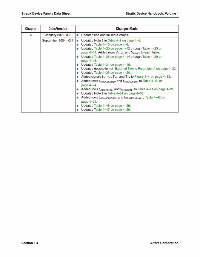
Chapter Date/Version Changes Made
1 July 2005, v3.2 ● Minor content changes.
September 2004, v3.1 ● Updated Table 1–6 on page 1–5.
April 2004, v3.0 ● Main section page numbers changed on first page.● Changed PCI-X to PCI-X 1.0 in “Features” on page 1–2.● Global change from SignalTap to SignalTap II.● The DSP blocks in “Features” on page 1–2 provide dedicated
implementation of multipliers that are now “faster than 300 MHz.”
January 2004, v2.2 ● Updated -5 speed grade device information in Table 1-6.
October 2003, v2.1 ● Add -8 speed grade device information.
July 2003, v2.0 ● Format changes throughout chapter.

Section I–2 Altera Corporation
Stratix Device Family Data Sheet Stratix Device Handbook, Volume 1
2 July 2005 v3.2 ● Added “Clear Signals” section.● Updated “Power Sequencing & Hot Socketing” section.● Format changes.
September 2004, v3.1 ● Updated fast regional clock networks description on page 2–73.● Deleted the word preliminary from the “specification for the maximum
time to relock is 100 µs” on page 2–90.● Added information about differential SSTL and HSTL outputs in
“External Clock Outputs” on page 2–92.● Updated notes in Figure 2–55 on page 2–93.● Added information about m counter to “Clock Multiplication &
Division” on page 2–101.● Updated Note 1 in Table 2–58 on page 2–101.● Updated description of “Clock Multiplication & Division” on
page 2–88.● Updated Table 2–22 on page 2–102.● Added references to AN 349 and AN 329 to “External RAM
Interfacing” on page 2–115.● Table 2–25 on page 2–116: updated the table, updated Notes 3 and
4. Notes 4, 5, and 6, are now Notes 5, 6, and 7, respectively.● Updated Table 2–26 on page 2–117.● Added information about PCI Compliance to page 2–120.● Table 2–32 on page 2–126: updated the table and deleted Note 1.● Updated reference to device pin-outs now being available on the web
on page 2–130.● Added Notes 4 and 5 to Table 2–36 on page 2–130.● Updated Note 3 in Table 2–37 on page 2–131.● Updated Note 5 in Table 2–41 on page 2–135.
April 2004, v3.0 ● Added note 3 to rows 11 and 12 in Table 2–18.● Deleted “Stratix and Stratix GX Device PLL Availability” table.● Added I/O standards row in Table 2–28 that support max and min
strength.● Row clk [1,3,8,10] was removed from Table 2–30.● Added checkmarks in Enhanced column for LVPECL, 3.3-V PCML,
LVDS, and HyperTransport technology rows in Table 2–32.● Removed the Left and Right I/O Banks row in Table 2–34.● Changed RCLK values in Figures 2–50 and 2–51.● External RAM Interfacing section replaced.
November 2003, v2.2 ● Added 672-pin BGA package information in Table 2–37.● Removed support for series and parallel on-chip termination.● Termination Technology renamed differential on-chip termination.● Updated the number of channels per PLL in Tables 2-38 through 2-
42.● Updated Figures 2–65 and 2–67.
October 2003, v2.1 ● Updated DDR I information.● Updated Table 2–22.● Added Tables 2–25, 2–29, 2–30, and 2–72.● Updated Figures 2–59, 2–65, and 2–67.● Updated the Lock Detect section.
Chapter Date/Version Changes Made

Altera Corporation Section I–3
Stratix Device Family Data Sheet
2 July 2003, v2.0 ● Added reference on page 2-73 to Figures 2-50 and 2-51 for RCLK connections.
● Updated ranges for EPLL post-scale and pre-scale dividers on page 2-85.
● Updated PLL Reconfiguration frequency from 25 to 22 MHz on page 2-87.
● New requirement to assert are set signal each PLL when it has to re-acquire lock on either a new clock after loss of lock (page 2-96).
● Updated max input frequency for CLK[1,3,8,10] from 462 to 500, Table 2-24.
● Renamed impedance matching to series termination throughout.● Updated naming convention for DQS pins on page 2-112 to match pin
tables.● Added DDR SDRAM Performance Specification on page 2-117.● Added external reference resistor values for terminator technology
(page 2-136).● Added Terminator Technology Specification on pages 2-137 and 2-
138.● Updated Tables 2-45 to 2-49 to reflect PLL cross-bank support for
high speed differential channels at full speed. ● Wire bond package performance specification for “high” speed
channels was increased to 624 Mbps from 462 Mbps throughout chapter.
3 July 2005, v1.3 ● Updated “Operating Modes” section.● Updated “Temperature Sensing Diode” section.● Updated “IEEE Std. 1149.1 (JTAG) Boundary-Scan Support” section.● Updated “Configuration” section.
January 2005, v1.2 ● Updated limits for JTAG chain of devices.
September 2004, v1.1 ● Added new section, “Stratix Automated Single Event Upset (SEU) Detection” on page 3–12.
● Updated description of “Custom-Built Circuitry” on page 3–13.
April 2003, v1.0 ● No new changes in Stratix Device Handbook v2.0.
4 January 2006, v3.4 ● Added Table 4–135.
July 2005, v3.3 ● Updated Tables 4–6 and 4–30.● Updated Tables 4–103 through 4–108.● Updated Tables 4–114 through 4–124.● Updated Table 4–129.● Added Table 4–130.
Chapter Date/Version Changes Made
Section I–4 Altera Corporation
Stratix Device Family Data Sheet Stratix Device Handbook, Volume 1
4 January 2005, 3.2 ● Updated rise and fall input values.
September 2004, v3.1 ● Updated Note 3 in Table 4–8 on page 4–4.● Updated Table 4–10 on page 4–6.● Updated Table 4–20 on page 4–12 through Table 4–23 on
page 4–13. Added rows VIL(AC) and VIH(AC) to each table.● Updated Table 4–26 on page 4–14 through Table 4–29 on
page 4–15.● Updated Table 4–31 on page 4–16.● Updated description of “External Timing Parameters” on page 4–33.● Updated Table 4–36 on page 4–20.● Added signals tOUTCO, TXZ, and TZX to Figure 4–4 on page 4–33.● Added rows tM512CLKENSU and tM512CLKENH to Table 4–40 on
page 4–24.● Added rows tM4CLKENSU and tM4CLKENH to Table 4–41 on page 4–24.● Updated Note 2 in Table 4–54 on page 4–35.● Added rows tMRAMCLKENSU and tMRAMCLKENH to Table 4–42 on
page 4–25.● Updated Table 4–46 on page 4–29.● Updated Table 4–47 on page 4–29.
Chapter Date/Version Changes Made

Altera Corporation Section I–5
Stratix Device Family Data Sheet
4 ● Table 4–48 on page 4–30: added rows tM512CLKSENSU and tM512CLKENH, and updated symbol names.
● Updated power-up current (ICCINT) required to power a Stratix device on page 4–17.
● Updated Table 4–37 on page 4–22 through Table 4–43 on page 4–27.
● Table 4–49 on page 4–31: added rows tM4KCLKENSU, tM4KCLKENH, tM4KBESU, and tM4KBEH, deleted rows tM4KRADDRASU and tM4KRADDRH, and updated symbol names.
● Table 4–50 on page 4–31: added rows tMRAMCLKENSU, tMRAMCLKENH, tMRAMBESU, and tMRAMBEH, deleted rows tMRAMADDRASU and tMRAMRADDRH, and updated symbol names.
● Table 4–52 on page 4–34: updated table, deleted “Conditions” column, and added rows tXZ and tZX.
● Table 4–52 on page 4–34: updated table, deleted “Conditions” column, and added rows tXZ and tZX.
● Table 4–53 on page 4–34: updated table and added rows tXZPLL and tZXPLL.
● Updated Note 2 in Table 4–53 on page 4–34.● Table 4–54 on page 4–35: updated table, deleted “Conditions”
column, and added rows tXZPLL and tZXPLL.● Updated Note 2 in Table 4–54 on page 4–35.● Deleted Note 2 from Table 4–55 on page 4–36 through Table 4–66 on
page 4–41.● Updated Table 4–55 on page 4–36 through Table 4–96 on
page 4–56. Added rows TXZ, TZX, TXZPLL, and TZXPLL.
● Added Note 4 to Table 4–101 on page 4–62.● Deleted Note 1 from Table 4–67 on page 4–42 through Table 4–84 on
page 4–50.● Added new section “I/O Timing Measurement Methodology” on
page 4–60.● Deleted Note 1 from Table 4–67 on page 4–42 through Table 4–84 on
page 4–50.● Deleted Note 2 from Table 4–85 on page 4–51 through Table 4–96 on
page 4–56.● Added Note 4 to Table 4–101 on page 4–62.● Table 4–102 on page 4–64: updated table and added Note 4.● Updated description of “External I/O Delay Parameters” on
page 4–66.● Added Note 1 to Table 4–109 on page 4–73 and Table 4–110 on
page 4–74.● Updated Table 4–103 on page 4–66 through Table 4–110 on
page 4–74.● Deleted Note 2 from Table 4–103 on page 4–66 through Table 4–106
on page 4–69.● Added new paragraph about output adder delays on page 4–68.● Updated Table 4–110 on page 4–74.● Added Note 1 to Table 4–111 through Table 4–113 on page 4–75.
Chapter Date/Version Changes Made
Section I–6 Altera Corporation
Stratix Device Family Data Sheet Stratix Device Handbook, Volume 1
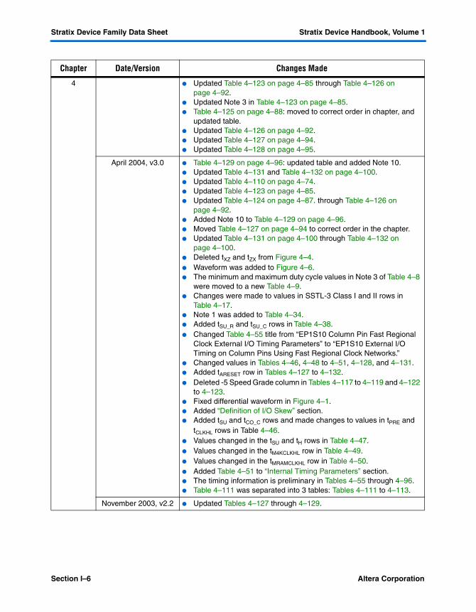
4 ● Updated Table 4–123 on page 4–85 through Table 4–126 on page 4–92.
● Updated Note 3 in Table 4–123 on page 4–85.● Table 4–125 on page 4–88: moved to correct order in chapter, and
updated table.● Updated Table 4–126 on page 4–92.● Updated Table 4–127 on page 4–94.● Updated Table 4–128 on page 4–95.
April 2004, v3.0 ● Table 4–129 on page 4–96: updated table and added Note 10.● Updated Table 4–131 and Table 4–132 on page 4–100.● Updated Table 4–110 on page 4–74.● Updated Table 4–123 on page 4–85.● Updated Table 4–124 on page 4–87. through Table 4–126 on
page 4–92.● Added Note 10 to Table 4–129 on page 4–96.● Moved Table 4–127 on page 4–94 to correct order in the chapter.● Updated Table 4–131 on page 4–100 through Table 4–132 on
page 4–100.● Deleted tXZ and tZX from Figure 4–4.● Waveform was added to Figure 4–6.● The minimum and maximum duty cycle values in Note 3 of Table 4–8
were moved to a new Table 4–9.● Changes were made to values in SSTL-3 Class I and II rows in
Table 4–17.● Note 1 was added to Table 4–34.● Added tSU_R and tSU_C rows in Table 4–38.● Changed Table 4–55 title from “EP1S10 Column Pin Fast Regional
Clock External I/O Timing Parameters” to “EP1S10 External I/O Timing on Column Pins Using Fast Regional Clock Networks.”
● Changed values in Tables 4–46, 4–48 to 4–51, 4–128, and 4–131.● Added tARESET row in Tables 4–127 to 4–132.● Deleted -5 Speed Grade column in Tables 4–117 to 4–119 and 4–122
to 4–123.● Fixed differential waveform in Figure 4–1.● Added “Definition of I/O Skew” section.● Added tSU and tCO_C rows and made changes to values in tPRE and
tCLKHL rows in Table 4–46.● Values changed in the tSU and tH rows in Table 4–47.● Values changed in the tM4KCLKHL row in Table 4–49.● Values changed in the tMRAMCLKHL row in Table 4–50.● Added Table 4–51 to “Internal Timing Parameters” section.● The timing information is preliminary in Tables 4–55 through 4–96. ● Table 4–111 was separated into 3 tables: Tables 4–111 to 4–113.
November 2003, v2.2 ● Updated Tables 4–127 through 4–129.
Chapter Date/Version Changes Made
Altera Corporation Section I–7
Stratix Device Family Data Sheet
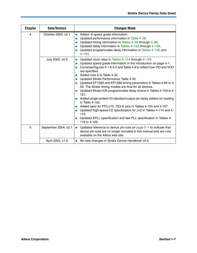
4 October 2003, v2.1 ● Added -8 speed grade information.● Updated performance information in Table 4–36.● Updated timing information in Tables 4–55 through 4–96.● Updated delay information in Tables 4–103 through 4–108.● Updated programmable delay information in Tables 4–100 and
4–103.
July 2003, v2.0 ● Updated clock rates in Tables 4–114 through 4–123.● Updated speed grade information in the introduction on page 4-1.● Corrected figures 4-1 & 4-2 and Table 4-9 to reflect how VID and VOD
are specified.● Added note 6 to Table 4-32.● Updated Stratix Performance Table 4-35.● Updated EP1S60 and EP1S80 timing parameters in Tables 4-82 to 4-
93. The Stratix timing models are final for all devices.● Updated Stratix IOE programmable delay chains in Tables 4-100 to 4-
101.● Added single-ended I/O standard output pin delay adders for loading
in Table 4-102.● Added spec for FPLL[10..7]CLK pins in Tables 4-104 and 4-107.● Updated high-speed I/O specification for J=2 in Tables 4-114 and 4-
115. ● Updated EPLL specification and fast PLL specification in Tables 4-
116 to 4-120.
5 September 2004, v2.1 ● Updated reference to device pin-outs on page 5–1 to indicate that device pin-outs are no longer included in this manual and are now available on the Altera web site.
April 2003, v1.0 ● No new changes in Stratix Device Handbook v2.0.
Chapter Date/Version Changes Made

Section I–8 Altera Corporation
Stratix Device Family Data Sheet Stratix Device Handbook, Volume 1

Altera Corporation 1–1July 2005
1. Introduction
Introduction The Stratix® family of FPGAs is based on a 1.5-V, 0.13-µm, all-layer copper SRAM process, with densities of up to 79,040 logic elements (LEs) and up to 7.5 Mbits of RAM. Stratix devices offer up to 22 digital signal processing (DSP) blocks with up to 176 (9-bit × 9-bit) embedded multipliers, optimized for DSP applications that enable efficient implementation of high-performance filters and multipliers. Stratix devices support various I/O standards and also offer a complete clock management solution with its hierarchical clock structure with up to 420-MHz performance and up to 12 phase-locked loops (PLLs).
The following shows the main sections in the Stratix Device Family Data Sheet:
Section Page
Features . . . . . . . . . . . . . . . . . . . . . . . . . . . . . . . . . . . . . . . . . . . . . 1–2
Functional Description . . . . . . . . . . . . . . . . . . . . . . . . . . . . . . . . 2–1Logic Array Blocks. . . . . . . . . . . . . . . . . . . . . . . . . . . . . . . . . . . . 2–3Logic Elements . . . . . . . . . . . . . . . . . . . . . . . . . . . . . . . . . . . . . . . 2–6MultiTrack Interconnect . . . . . . . . . . . . . . . . . . . . . . . . . . . . . . 2–14TriMatrix Memory . . . . . . . . . . . . . . . . . . . . . . . . . . . . . . . . . . . 2–21Digital Signal Processing Block . . . . . . . . . . . . . . . . . . . . . . . . 2–52PLLs & Clock Networks . . . . . . . . . . . . . . . . . . . . . . . . . . . . . . 2–73I/O Structure . . . . . . . . . . . . . . . . . . . . . . . . . . . . . . . . . . . . . . 2–104High-Speed Differential I/O Support. . . . . . . . . . . . . . . . . . 2–130Power Sequencing & Hot Socketing . . . . . . . . . . . . . . . . . . . 2–140
IEEE Std. 1149.1 (JTAG) Boundary-Scan Support. . . . . . . . . . 3–1SignalTap II Embedded Logic Analyzer . . . . . . . . . . . . . . . . . 3–5Configuration . . . . . . . . . . . . . . . . . . . . . . . . . . . . . . . . . . . . . . . . 3–5Temperature Sensing Diode. . . . . . . . . . . . . . . . . . . . . . . . . . . 3–13
Operating Conditions . . . . . . . . . . . . . . . . . . . . . . . . . . . . . . . . . 4–1Power Consumption . . . . . . . . . . . . . . . . . . . . . . . . . . . . . . . . . 4–17Timing Model . . . . . . . . . . . . . . . . . . . . . . . . . . . . . . . . . . . . . . . 4–19
Software. . . . . . . . . . . . . . . . . . . . . . . . . . . . . . . . . . . . . . . . . . . . . 5–1Device Pin-Outs . . . . . . . . . . . . . . . . . . . . . . . . . . . . . . . . . . . . . . 5–1Ordering Information . . . . . . . . . . . . . . . . . . . . . . . . . . . . . . . . . 5–1
S51001-3.2

1–2 Altera CorporationStratix Device Handbook, Volume 1 July 2005
Features
Features The Stratix family offers the following features:
■ 10,570 to 79,040 LEs; see Table 1–1■ Up to 7,427,520 RAM bits (928,440 bytes) available without reducing
logic resources■ TriMatrixTM memory consisting of three RAM block sizes to
implement true dual-port memory and first-in first-out (FIFO) buffers
■ High-speed DSP blocks provide dedicated implementation of multipliers (faster than 300 MHz), multiply-accumulate functions, and finite impulse response (FIR) filters
■ Up to 16 global clocks with 22 clocking resources per device region■ Up to 12 PLLs (four enhanced PLLs and eight fast PLLs) per device
provide spread spectrum, programmable bandwidth, clock switch-over, real-time PLL reconfiguration, and advanced multiplication and phase shifting
■ Support for numerous single-ended and differential I/O standards■ High-speed differential I/O support on up to 116 channels with up
to 80 channels optimized for 840 megabits per second (Mbps)■ Support for high-speed networking and communications bus
standards including RapidIO, UTOPIA IV, CSIX, HyperTransportTM technology, 10G Ethernet XSBI, SPI-4 Phase 2 (POS-PHY Level 4), and SFI-4
■ Differential on-chip termination support for LVDS■ Support for high-speed external memory, including zero bus
turnaround (ZBT) SRAM, quad data rate (QDR and QDRII) SRAM, double data rate (DDR) SDRAM, DDR fast cycle RAM (FCRAM), and single data rate (SDR) SDRAM
■ Support for 66-MHz PCI (64 and 32 bit) in -6 and faster speed-grade devices, support for 33-MHz PCI (64 and 32 bit) in -8 and faster speed-grade devices
■ Support for 133-MHz PCI-X 1.0 in -5 speed-grade devices■ Support for 100-MHz PCI-X 1.0 in -6 and faster speed-grade devices■ Support for 66-MHz PCI-X 1.0 in -7 speed-grade devices■ Support for multiple intellectual property megafunctions from
Altera MegaCore® functions and Altera Megafunction Partners Program (AMPPSM) megafunctions
■ Support for remote configuration updates

Altera Corporation 1–3July 2005 Stratix Device Handbook, Volume 1
Introduction
Table 1–1. Stratix Device Features — EP1S10, EP1S20, EP1S25, EP1S30
Feature EP1S10 EP1S20 EP1S25 EP1S30
LEs 10,570 18,460 25,660 32,470
M512 RAM blocks (32 × 18 bits) 94 194 224 295
M4K RAM blocks (128 × 36 bits) 60 82 138 171
M-RAM blocks (4K × 144 bits) 1 2 2 4
Total RAM bits 920,448 1,669,248 1,944,576 3,317,184
DSP blocks 6 10 10 12
Embedded multipliers (1) 48 80 80 96
PLLs 6 6 6 10
Maximum user I/O pins 426 586 706 726
Table 1–2. Stratix Device Features — EP1S40, EP1S60, EP1S80
Feature EP1S40 EP1S60 EP1S80
LEs 41,250 57,120 79,040
M512 RAM blocks (32 × 18 bits) 384 574 767
M4K RAM blocks (128 × 36 bits) 183 292 364
M-RAM blocks (4K × 144 bits) 4 6 9
Total RAM bits 3,423,744 5,215,104 7,427,520
DSP blocks 14 18 22
Embedded multipliers (1) 112 144 176
PLLs 12 12 12
Maximum user I/O pins 822 1,022 1,238
Note to Tables 1–1 and 1–2:(1) This parameter lists the total number of 9 × 9-bit multipliers for each device. For the total number of 18 × 18-bit
multipliers per device, divide the total number of 9 × 9-bit multipliers by 2. For the total number of 36 × 36-bit multipliers per device, divide the total number of 9 × 9-bit multipliers by 8.

1–4 Altera CorporationStratix Device Handbook, Volume 1 July 2005
Features
Stratix devices are available in space-saving FineLine BGA® and ball-grid array (BGA) packages (see Tables 1–3 through 1–5). All Stratix devices support vertical migration within the same package (for example, you can migrate between the EP1S10, EP1S20, and EP1S25 devices in the 672-pin BGA package). Vertical migration means that you can migrate to devices whose dedicated pins, configuration pins, and power pins are the same for a given package across device densities. For I/O pin migration across densities, you must cross-reference the available I/O pins using the device pin-outs for all planned densities of a given package type to identify which I/O pins are migrational. The Quartus® II software can automatically cross reference and place all pins except differential pins for migration when given a device migration list. You must use the pin-outs for each device to verify the differential placement migration. A future version of the Quartus II software will support differential pin migration.
Table 1–3. Stratix Package Options & I/O Pin Counts
Device 672-Pin BGA
956-Pin BGA
484-Pin FineLine
BGA
672-Pin FineLine
BGA
780-Pin FineLine
BGA
1,020-Pin FineLine
BGA
1,508-Pin FineLine
BGA
EP1S10 345 335 345 426
EP1S20 426 361 426 586
EP1S25 473 473 597 706
EP1S30 683 597 726
EP1S40 683 615 773 822
EP1S60 683 773 1,022
EP1S80 683 773 1,203
Note to Table 1–3:(1) All I/O pin counts include 20 dedicated clock input pins (clk[15..0]p, clk0n, clk2n, clk9n, and clk11n)
that can be used for data inputs.
Table 1–4. Stratix BGA Package Sizes
Dimension 672 Pin 956 Pin
Pitch (mm) 1.27 1.27
Area (mm2) 1,225 1,600
Length × width (mm × mm) 35 × 35 40 × 40

Altera Corporation 1–5July 2005 Stratix Device Handbook, Volume 1
Introduction
Stratix devices are available in up to four speed grades, -5, -6, -7, and -8, with -5 being the fastest. Table 1–6 shows Stratix device speed-grade offerings.
Table 1–5. Stratix FineLine BGA Package Sizes
Dimension 484 Pin 672 Pin 780 Pin 1,020 Pin 1,508 Pin
Pitch (mm) 1.00 1.00 1.00 1.00 1.00
Area (mm2) 529 729 841 1,089 1,600
Length × width (mm × mm)
23 × 23 27 × 27 29 × 29 33 × 33 40 × 40
Table 1–6. Stratix Device Speed Grades
Device 672-Pin BGA
956-Pin BGA
484-Pin FineLine
BGA
672-Pin FineLine
BGA
780-Pin FineLine
BGA
1,020-Pin FineLine
BGA
1,508-Pin FineLine
BGA
EP1S10 -6, -7 -5, -6, -7 -6, -7 -5, -6, -7
EP1S20 -6, -7 -5, -6, -7 -6, -7 -5, -6, -7
EP1S25 -6, -7 -6, -7, -8 -5, -6, -7 -5, -6, -7
EP1S30 -5, -6, -7 -5, -6, -7, -8 -5, -6, -7
EP1S40 -5, -6, -7 -5, -6, -7, -8 -5, -6, -7 -5, -6, -7
EP1S60 -6, -7 -5, -6, -7 -6, -7
EP1S80 -6, -7 -5, -6, -7 -5, -6, -7

1–6 Altera CorporationStratix Device Handbook, Volume 1 July 2005
Features

Altera Corporation 2–1July 2005
2. Stratix Architecture
Functional Description
Stratix® devices contain a two-dimensional row- and column-based architecture to implement custom logic. A series of column and row interconnects of varying length and speed provide signal interconnects between logic array blocks (LABs), memory block structures, and DSP blocks.
The logic array consists of LABs, with 10 logic elements (LEs) in each LAB. An LE is a small unit of logic providing efficient implementation of user logic functions. LABs are grouped into rows and columns across the device.
M512 RAM blocks are simple dual-port memory blocks with 512 bits plus parity (576 bits). These blocks provide dedicated simple dual-port or single-port memory up to 18-bits wide at up to 318 MHz. M512 blocks are grouped into columns across the device in between certain LABs.
M4K RAM blocks are true dual-port memory blocks with 4K bits plus parity (4,608 bits). These blocks provide dedicated true dual-port, simple dual-port, or single-port memory up to 36-bits wide at up to 291 MHz. These blocks are grouped into columns across the device in between certain LABs.
M-RAM blocks are true dual-port memory blocks with 512K bits plus parity (589,824 bits). These blocks provide dedicated true dual-port, simple dual-port, or single-port memory up to 144-bits wide at up to 269 MHz. Several M-RAM blocks are located individually or in pairs within the device’s logic array.
Digital signal processing (DSP) blocks can implement up to either eight full-precision 9 × 9-bit multipliers, four full-precision 18 × 18-bit multipliers, or one full-precision 36 × 36-bit multiplier with add or subtract features. These blocks also contain 18-bit input shift registers for digital signal processing applications, including FIR and infinite impulse response (IIR) filters. DSP blocks are grouped into two columns in each device.
Each Stratix device I/O pin is fed by an I/O element (IOE) located at the end of LAB rows and columns around the periphery of the device. I/O pins support numerous single-ended and differential I/O standards. Each IOE contains a bidirectional I/O buffer and six registers for registering input, output, and output-enable signals. When used with
S51002-3.2

2–2 Altera CorporationStratix Device Handbook, Volume 1 July 2005
Functional Description
dedicated clocks, these registers provide exceptional performance and interface support with external memory devices such as DDR SDRAM, FCRAM, ZBT, and QDR SRAM devices.
High-speed serial interface channels support transfers at up to 840 Mbps using LVDS, LVPECL, 3.3-V PCML, or HyperTransport technology I/O standards.
Figure 2–1 shows an overview of the Stratix device.
Figure 2–1. Stratix Block Diagram
M512 RAM Blocks for Dual-Port Memory, Shift Registers, & FIFO Buffers
DSP Blocks forMultiplication and FullImplementation of FIR Filters
M4K RAM Blocksfor True Dual-Port Memory & Other EmbeddedMemory Functions
IOEs Support DDR, PCI, GTL+, SSTL-3, SSTL-2, HSTL, LVDS, LVPECL, PCML, HyperTransport & other I/O Standards
IOEs
IOEs
IOEs
IOEs
IOEs
IOEs
IOEs
IOEs
IOEs
IOEs
IOEs
IOEs
IOEs
IOEs
IOEs
IOEs
IOEs
LABs
LABs
IOEs
LABs
LABs
LABs
LABs
LABs
LABs
LABs
LABs
LABs
LABs
LABs
LABs
LABs
LABs
LABs
LABs
LABs
IOEs
LABs
LABs
LABs
LABs
LABs
LABs
LABs
LABs
LABs
LABs
LABs
LABs
LABs
LABs
LABs
LABs LABs
LABs
IOEs IOEs
LABs
LABs LABs
LABs LABs
LABs
LABs
LABs
LABs
LABs
LABs
LABs
LABs
LABs
LABs
LABs
LABs
LABs
LABs
LABs LABs
LABs
LABs
LABs
LABs
LABs
LABs
LABs
LABs
LABs
LABs
LABs
LABs
LABs
LABs
LABs
LABs
LABs
LABs
LABs
LABs
DSPBlock
M-RAM Block
Altera Corporation 2–3July 2005 Stratix Device Handbook, Volume 1
Stratix Architecture
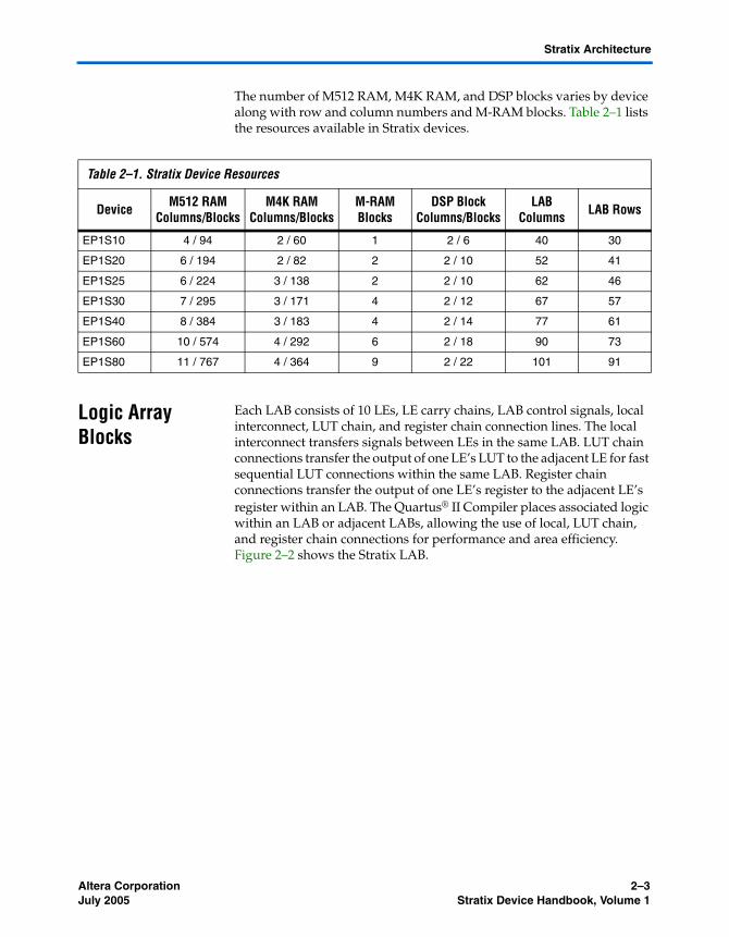
The number of M512 RAM, M4K RAM, and DSP blocks varies by device along with row and column numbers and M-RAM blocks. Table 2–1 lists the resources available in Stratix devices.
Logic Array Blocks
Each LAB consists of 10 LEs, LE carry chains, LAB control signals, local interconnect, LUT chain, and register chain connection lines. The local interconnect transfers signals between LEs in the same LAB. LUT chain connections transfer the output of one LE’s LUT to the adjacent LE for fast sequential LUT connections within the same LAB. Register chain connections transfer the output of one LE’s register to the adjacent LE’s register within an LAB. The Quartus® II Compiler places associated logic within an LAB or adjacent LABs, allowing the use of local, LUT chain, and register chain connections for performance and area efficiency. Figure 2–2 shows the Stratix LAB.
Table 2–1. Stratix Device Resources
Device M512 RAM Columns/Blocks
M4K RAM Columns/Blocks
M-RAM Blocks
DSP Block Columns/Blocks
LAB Columns LAB Rows
EP1S10 4 / 94 2 / 60 1 2 / 6 40 30
EP1S20 6 / 194 2 / 82 2 2 / 10 52 41
EP1S25 6 / 224 3 / 138 2 2 / 10 62 46
EP1S30 7 / 295 3 / 171 4 2 / 12 67 57
EP1S40 8 / 384 3 / 183 4 2 / 14 77 61
EP1S60 10 / 574 4 / 292 6 2 / 18 90 73
EP1S80 11 / 767 4 / 364 9 2 / 22 101 91

2–4 Altera CorporationStratix Device Handbook, Volume 1 July 2005
Logic Array Blocks
Figure 2–2. Stratix LAB Structure
LAB Interconnects
The LAB local interconnect can drive LEs within the same LAB. The LAB local interconnect is driven by column and row interconnects and LE outputs within the same LAB. Neighboring LABs, M512 RAM blocks, M4K RAM blocks, or DSP blocks from the left and right can also drive an LAB’s local interconnect through the direct link connection. The direct link connection feature minimizes the use of row and column interconnects, providing higher performance and flexibility. Each LE can drive 30 other LEs through fast local and direct link interconnects. Figure 2–3 shows the direct link connection.
Direct linkinterconnect fromadjacent block
Direct linkinterconnect toadjacent block
Row Interconnects ofVariable Speed & Length
Column Interconnects ofVariable Speed & Length
Three-Sided Architecture—LocalInterconnect is Driven from Either Side byColumns & LABs, & from Above by Rows
Local Interconnect LAB
Direct linkinterconnect from adjacent block
Direct linkinterconnect toadjacent block

Altera Corporation 2–5July 2005 Stratix Device Handbook, Volume 1
Stratix Architecture
Figure 2–3. Direct Link Connection
LAB Control Signals
Each LAB contains dedicated logic for driving control signals to its LEs. The control signals include two clocks, two clock enables, two asynchronous clears, synchronous clear, asynchronous preset/load, synchronous load, and add/subtract control signals. This gives a maximum of 10 control signals at a time. Although synchronous load and clear signals are generally used when implementing counters, they can also be used with other functions.
Each LAB can use two clocks and two clock enable signals. Each LAB’s clock and clock enable signals are linked. For example, any LE in a particular LAB using the labclk1 signal will also use labclkena1. If the LAB uses both the rising and falling edges of a clock, it also uses both LAB-wide clock signals. De-asserting the clock enable signal will turn off the LAB-wide clock.
Each LAB can use two asynchronous clear signals and an asynchronous load/preset signal. The asynchronous load acts as a preset when the asynchronous load data input is tied high.
LAB
Direct linkinterconnectto right
Direct link interconnect fromright LAB, TriMatrix memoryblock, DSP block, or IOE output
Direct link interconnect fromleft LAB, TriMatrix memory
block, DSP block, or IOE output
LocalInterconnect
Direct linkinterconnect
to left

2–6 Altera CorporationStratix Device Handbook, Volume 1 July 2005
Logic Elements
With the LAB-wide addnsub control signal, a single LE can implement a one-bit adder and subtractor. This saves LE resources and improves performance for logic functions such as DSP correlators and signed multipliers that alternate between addition and subtraction depending on data.
The LAB row clocks [7..0] and LAB local interconnect generate the LAB-wide control signals. The MultiTrackTM interconnect’s inherent low skew allows clock and control signal distribution in addition to data. Figure 2–4 shows the LAB control signal generation circuit.
Figure 2–4. LAB-Wide Control Signals
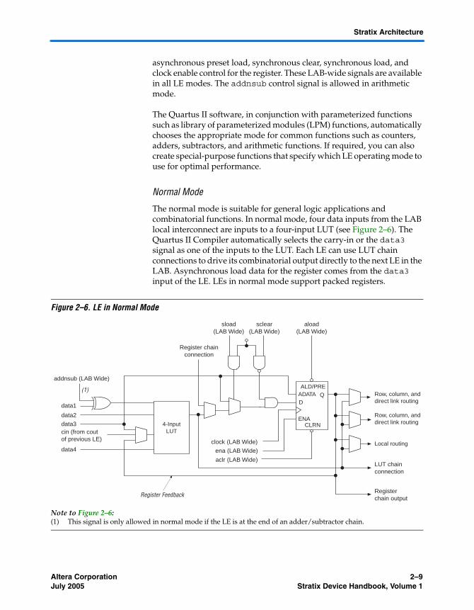
Logic Elements The smallest unit of logic in the Stratix architecture, the LE, is compact and provides advanced features with efficient logic utilization. Each LE contains a four-input LUT, which is a function generator that can implement any function of four variables. In addition, each LE contains a programmable register and carry chain with carry select capability. A single LE also supports dynamic single bit addition or subtraction mode selectable by an LAB-wide control signal. Each LE drives all types of interconnects: local, row, column, LUT chain, register chain, and direct link interconnects. See Figure 2–5.
labclkena1
labclk2labclk1
labclkena2
asyncloador labpre
syncload
DedicatedRow LABClocks
LocalInterconnect
LocalInterconnect
LocalInterconnect
LocalInterconnect
LocalInterconnect
LocalInterconnect
labclr1
labclr2
synclr
addnsub
8

Altera Corporation 2–7July 2005 Stratix Device Handbook, Volume 1
Stratix Architecture
Figure 2–5. Stratix LE
Each LE’s programmable register can be configured for D, T, JK, or SR operation. Each register has data, true asynchronous load data, clock, clock enable, clear, and asynchronous load/preset inputs. Global signals, general-purpose I/O pins, or any internal logic can drive the register’s clock and clear control signals. Either general-purpose I/O pins or internal logic can drive the clock enable, preset, asynchronous load, and asynchronous data. The asynchronous load data input comes from the data3 input of the LE. For combinatorial functions, the register is bypassed and the output of the LUT drives directly to the outputs of the LE.
Each LE has three outputs that drive the local, row, and column routing resources. The LUT or register output can drive these three outputs independently. Two LE outputs drive column or row and direct link routing connections and one drives local interconnect resources. This allows the LUT to drive one output while the register drives another output. This feature, called register packing, improves device utilization because the device can use the register and the LUT for unrelated
labclk1
labclk2
labclr2labpre/aload
Carry-In1
Carry-In0
LAB Carry-In
Clock &Clock Enable
Select
LAB Carry-Out
Carry-Out1
Carry-Out0
Look-UpTable(LUT)
CarryChain
Row, column,and direct link routing
Row, column,and direct link routing
ProgrammableRegister
PRN/ALD
CLRN
D Q
ENA
Register Bypass
PackedRegister Select
Chip-WideReset
labclkena1labclkena2
SynchronousLoad andClear Logic
LAB-wideSynchronous
LoadLAB-wide
SynchronousClear
AsynchronousClear/Preset/Load Logic
data1
data2data3
data4
LUT chainrouting to next LE
labclr1
Local Routing
Register chainoutput
ADATA
addnsub
RegisterFeedback
Register chainrouting fromprevious LE

2–8 Altera CorporationStratix Device Handbook, Volume 1 July 2005
Logic Elements
functions. Another special packing mode allows the register output to feed back into the LUT of the same LE so that the register is packed with its own fan-out LUT. This provides another mechanism for improved fitting. The LE can also drive out registered and unregistered versions of the LUT output.
LUT Chain & Register Chain
In addition to the three general routing outputs, the LEs within an LAB have LUT chain and register chain outputs. LUT chain connections allow LUTs within the same LAB to cascade together for wide input functions. Register chain outputs allow registers within the same LAB to cascade together. The register chain output allows an LAB to use LUTs for a single combinatorial function and the registers to be used for an unrelated shift register implementation. These resources speed up connections between LABs while saving local interconnect resources. See “MultiTrack Interconnect” on page 2–14 for more information on LUT chain and register chain connections.
addnsub Signal
The LE’s dynamic adder/subtractor feature saves logic resources by using one set of LEs to implement both an adder and a subtractor. This feature is controlled by the LAB-wide control signal addnsub. The addnsub signal sets the LAB to perform either A + B or A – B. The LUT computes addition, and subtraction is computed by adding the two’s complement of the intended subtractor. The LAB-wide signal converts to two’s complement by inverting the B bits within the LAB and setting carry-in = 1 to add one to the least significant bit (LSB). The LSB of an adder/subtractor must be placed in the first LE of the LAB, where the LAB-wide addnsub signal automatically sets the carry-in to 1. The Quartus II Compiler automatically places and uses the adder/subtractor feature when using adder/subtractor parameterized functions.
LE Operating Modes
The Stratix LE can operate in one of the following modes:
■ Normal mode■ Dynamic arithmetic mode
Each mode uses LE resources differently. In each mode, eight available inputs to the LE—the four data inputs from the LAB local interconnect; carry-in0 and carry-in1 from the previous LE; the LAB carry-in from the previous carry-chain LAB; and the register chain connection—are directed to different destinations to implement the desired logic function. LAB-wide signals provide clock, asynchronous clear,
Altera Corporation 2–9July 2005 Stratix Device Handbook, Volume 1
Stratix Architecture
asynchronous preset load, synchronous clear, synchronous load, and clock enable control for the register. These LAB-wide signals are available in all LE modes. The addnsub control signal is allowed in arithmetic mode.
The Quartus II software, in conjunction with parameterized functions such as library of parameterized modules (LPM) functions, automatically chooses the appropriate mode for common functions such as counters, adders, subtractors, and arithmetic functions. If required, you can also create special-purpose functions that specify which LE operating mode to use for optimal performance.
Normal Mode
The normal mode is suitable for general logic applications and combinatorial functions. In normal mode, four data inputs from the LAB local interconnect are inputs to a four-input LUT (see Figure 2–6). The Quartus II Compiler automatically selects the carry-in or the data3 signal as one of the inputs to the LUT. Each LE can use LUT chain connections to drive its combinatorial output directly to the next LE in the LAB. Asynchronous load data for the register comes from the data3 input of the LE. LEs in normal mode support packed registers.
Figure 2–6. LE in Normal Mode
Note to Figure 2–6:(1) This signal is only allowed in normal mode if the LE is at the end of an adder/subtractor chain.
data1
4-InputLUT
data2
data3cin (from coutof previous LE)
data4
addnsub (LAB Wide)
clock (LAB Wide)
ena (LAB Wide)
aclr (LAB Wide)
aload(LAB Wide)
ALD/PRE
CLRN
DQ
ENA
ADATA
sclear(LAB Wide)
sload(LAB Wide)
Register chainconnection
LUT chainconnection
Registerchain output
Row, column, anddirect link routing
Row, column, anddirect link routing
Local routing
Register Feedback
(1)

2–10 Altera CorporationStratix Device Handbook, Volume 1 July 2005
Logic Elements
Dynamic Arithmetic Mode
The dynamic arithmetic mode is ideal for implementing adders, counters, accumulators, wide parity functions, and comparators. An LE in dynamic arithmetic mode uses four 2-input LUTs configurable as a dynamic adder/subtractor. The first two 2-input LUTs compute two summations based on a possible carry-in of 1 or 0; the other two LUTs generate carry outputs for the two chains of the carry select circuitry. As shown in Figure 2–7, the LAB carry-in signal selects either the carry-in0 or carry-in1 chain. The selected chain’s logic level in turn determines which parallel sum is generated as a combinatorial or registered output. For example, when implementing an adder, the sum output is the selection of two possible calculated sums: data1 + data2 + carry-in0 or data1 + data2 + carry-in1. The other two LUTs use the data1 and data2 signals to generate two possible carry-out signals—one for a carry of 1 and the other for a carry of 0. The carry-in0 signal acts as the carry select for the carry-out0 output and carry-in1 acts as the carry select for the carry-out1 output. LEs in arithmetic mode can drive out registered and unregistered versions of the LUT output.
The dynamic arithmetic mode also offers clock enable, counter enable, synchronous up/down control, synchronous clear, synchronous load, and dynamic adder/subtractor options. The LAB local interconnect data inputs generate the counter enable and synchronous up/down control signals. The synchronous clear and synchronous load options are LAB-wide signals that affect all registers in the LAB. The Quartus II software automatically places any registers that are not used by the counter into other LABs. The addnsub LAB-wide signal controls whether the LE acts as an adder or subtractor.

Altera Corporation 2–11July 2005 Stratix Device Handbook, Volume 1
Stratix Architecture
Figure 2–7. LE in Dynamic Arithmetic Mode
Note to Figure 2–7:(1) The addnsub signal is tied to the carry input for the first LE of a carry chain only.
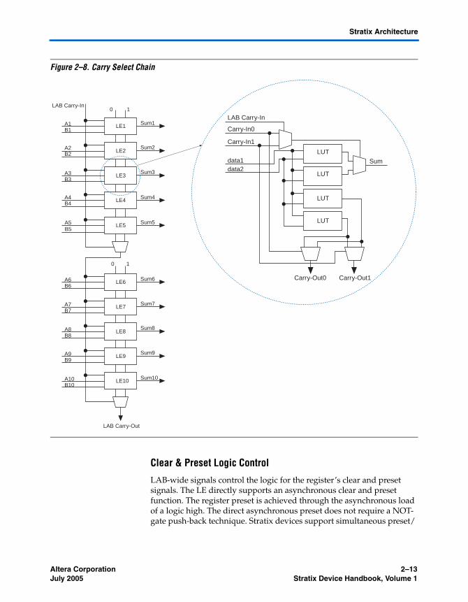
Carry-Select Chain
The carry-select chain provides a very fast carry-select function between LEs in arithmetic mode. The carry-select chain uses the redundant carry calculation to increase the speed of carry functions. The LE is configured to calculate outputs for a possible carry-in of 1 and carry-in of 0 in parallel. The carry-in0 and carry-in1 signals from a lower-order bit feed forward into the higher-order bit via the parallel carry chain and feed into both the LUT and the next portion of the carry chain. Carry-select chains can begin in any LE within an LAB.
The speed advantage of the carry-select chain is in the parallel pre-computation of carry chains. Since the LAB carry-in selects the precomputed carry chain, not every LE is in the critical path. Only the propagation delay between LAB carry-in generation (LE 5 and LE 10) are now part of the critical path. This feature allows the Stratix architecture to implement high-speed counters, adders, multipliers, parity functions, and comparators of arbitrary width.
data1 LUTdata2data3
addnsub(LAB Wide)
clock (LAB Wide)
ena (LAB Wide)
aclr (LAB Wide)
ALD/PRE
CLRN
DQ
ENA
ADATA
Register chainconnection
LUT
LUT
LUT
Carry-Out1Carry-Out0
LAB Carry-In
Carry-In0Carry-In1
(1)
sclear(LAB Wide)
sload(LAB Wide)
LUT chainconnection
Registerchain output
Row, column, anddirect link routing
Row, column, anddirect link routing
Local routing
aload(LAB Wide)
Register Feedback
2–12 Altera CorporationStratix Device Handbook, Volume 1 July 2005
Logic Elements
Figure 2–8 shows the carry-select circuitry in an LAB for a 10-bit full adder. One portion of the LUT generates the sum of two bits using the input signals and the appropriate carry-in bit; the sum is routed to the output of the LE. The register can be bypassed for simple adders or used for accumulator functions. Another portion of the LUT generates carry-out bits. An LAB-wide carry in bit selects which chain is used for the addition of given inputs. The carry-in signal for each chain, carry-in0 or carry-in1, selects the carry-out to carry forward to the carry-in signal of the next-higher-order bit. The final carry-out signal is routed to an LE, where it is fed to local, row, or column interconnects.
The Quartus II Compiler automatically creates carry chain logic during design processing, or you can create it manually during design entry. Parameterized functions such as LPM functions automatically take advantage of carry chains for the appropriate functions.
The Quartus II Compiler creates carry chains longer than 10 LEs by linking LABs together automatically. For enhanced fitting, a long carry chain runs vertically allowing fast horizontal connections to TriMatrix™ memory and DSP blocks. A carry chain can continue as far as a full column.
Altera Corporation 2–13July 2005 Stratix Device Handbook, Volume 1
Stratix Architecture
Figure 2–8. Carry Select Chain
Clear & Preset Logic Control
LAB-wide signals control the logic for the register’s clear and preset signals. The LE directly supports an asynchronous clear and preset function. The register preset is achieved through the asynchronous load of a logic high. The direct asynchronous preset does not require a NOT-gate push-back technique. Stratix devices support simultaneous preset/
LE4
LE3
LE2
LE1A1B1
A2B2
A3B3
A4B4
Sum1
Sum2
Sum3
Sum4
LE10
LE9
LE8
LE7A7B7
A8B8
A9B9
A10B10
Sum7
LE6A6B6
Sum6
LE5A5B5
Sum5
Sum8
Sum9
Sum10
0 1
0 1LAB Carry-In
LAB Carry-Out
LUT
LUT
LUT
LUT
data1
LAB Carry-In
data2
Carry-In0
Carry-In1
Carry-Out0 Carry-Out1
Sum

2–14 Altera CorporationStratix Device Handbook, Volume 1 July 2005
MultiTrack Interconnect
asynchronous load, and clear signals. An asynchronous clear signal takes precedence if both signals are asserted simultaneously. Each LAB supports up to two clears and one preset signal.
In addition to the clear and preset ports, Stratix devices provide a chip-wide reset pin (DEV_CLRn) that resets all registers in the device. An option set before compilation in the Quartus II software controls this pin. This chip-wide reset overrides all other control signals.
MultiTrack Interconnect
In the Stratix architecture, connections between LEs, TriMatrix memory, DSP blocks, and device I/O pins are provided by the MultiTrack interconnect structure with DirectDriveTM technology. The MultiTrack interconnect consists of continuous, performance-optimized routing lines of different lengths and speeds used for inter- and intra-design block connectivity. The Quartus II Compiler automatically places critical design paths on faster interconnects to improve design performance.
DirectDrive technology is a deterministic routing technology that ensures identical routing resource usage for any function regardless of placement within the device. The MultiTrack interconnect and DirectDrive technology simplify the integration stage of block-based designing by eliminating the re-optimization cycles that typically follow design changes and additions.
The MultiTrack interconnect consists of row and column interconnects that span fixed distances. A routing structure with fixed length resources for all devices allows predictable and repeatable performance when migrating through different device densities. Dedicated row interconnects route signals to and from LABs, DSP blocks, and TriMatrix memory within the same row. These row resources include:
■ Direct link interconnects between LABs and adjacent blocks.■ R4 interconnects traversing four blocks to the right or left.■ R8 interconnects traversing eight blocks to the right or left.■ R24 row interconnects for high-speed access across the length of the
device.
The direct link interconnect allows an LAB, DSP block, or TriMatrix memory block to drive into the local interconnect of its left and right neighbors and then back into itself. Only one side of a M-RAM block interfaces with direct link and row interconnects. This provides fast communication between adjacent LABs and/or blocks without using row interconnect resources.
The R4 interconnects span four LABs, three LABs and one M512 RAM block, two LABs and one M4K RAM block, or two LABs and one DSP block to the right or left of a source LAB. These resources are used for fast

Altera Corporation 2–15July 2005 Stratix Device Handbook, Volume 1
Stratix Architecture
row connections in a four-LAB region. Every LAB has its own set of R4 interconnects to drive either left or right. Figure 2–9 shows R4 interconnect connections from an LAB. R4 interconnects can drive and be driven by DSP blocks and RAM blocks and horizontal IOEs. For LAB interfacing, a primary LAB or LAB neighbor can drive a given R4 interconnect. For R4 interconnects that drive to the right, the primary LAB and right neighbor can drive on to the interconnect. For R4 interconnects that drive to the left, the primary LAB and its left neighbor can drive on to the interconnect. R4 interconnects can drive other R4 interconnects to extend the range of LABs they can drive. R4 interconnects can also drive C4 and C16 interconnects for connections from one row to another. Additionally, R4 interconnects can drive R24 interconnects.
Figure 2–9. R4 Interconnect Connections
Notes to Figure 2–9:(1) C4 interconnects can drive R4 interconnects.(2) This pattern is repeated for every LAB in the LAB row.
The R8 interconnects span eight LABs, M512 or M4K RAM blocks, or DSP blocks to the right or left from a source LAB. These resources are used for fast row connections in an eight-LAB region. Every LAB has its own set of R8 interconnects to drive either left or right. R8 interconnect connections between LABs in a row are similar to the R4 connections shown in Figure 2–9, with the exception that they connect to eight LABs to the right or left, not four. Like R4 interconnects, R8 interconnects can drive and be driven by all types of architecture blocks. R8 interconnects
PrimaryLAB (2)
R4 InterconnectDriving Left
Adjacent LAB canDrive onto AnotherLAB's R4 Interconnect
C4, C8, and C16Column Interconnects (1)
R4 InterconnectDriving Right
LABNeighbor
LABNeighbor

2–16 Altera CorporationStratix Device Handbook, Volume 1 July 2005
MultiTrack Interconnect
can drive other R8 interconnects to extend their range as well as C8 interconnects for row-to-row connections. One R8 interconnect is faster than two R4 interconnects connected together.
R24 row interconnects span 24 LABs and provide the fastest resource for long row connections between LABs, TriMatrix memory, DSP blocks, and IOEs. The R24 row interconnects can cross M-RAM blocks. R24 row interconnects drive to other row or column interconnects at every fourth LAB and do not drive directly to LAB local interconnects. R24 row interconnects drive LAB local interconnects via R4 and C4 interconnects. R24 interconnects can drive R24, R4, C16, and C4 interconnects.
The column interconnect operates similarly to the row interconnect and vertically routes signals to and from LABs, TriMatrix memory, DSP blocks, and IOEs. Each column of LABs is served by a dedicated column interconnect, which vertically routes signals to and from LABs, TriMatrix memory and DSP blocks, and horizontal IOEs. These column resources include:
■ LUT chain interconnects within an LAB■ Register chain interconnects within an LAB■ C4 interconnects traversing a distance of four blocks in up and down
direction■ C8 interconnects traversing a distance of eight blocks in up and
down direction■ C16 column interconnects for high-speed vertical routing through
the device
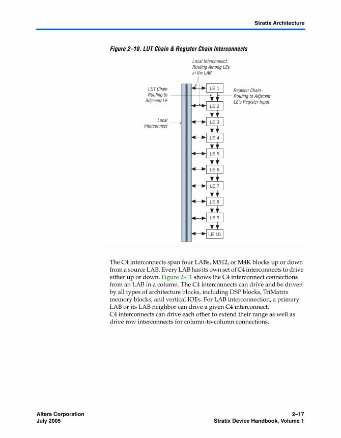
Stratix devices include an enhanced interconnect structure within LABs for routing LE output to LE input connections faster using LUT chain connections and register chain connections. The LUT chain connection allows the combinatorial output of an LE to directly drive the fast input of the LE right below it, bypassing the local interconnect. These resources can be used as a high-speed connection for wide fan-in functions from LE 1 to LE 10 in the same LAB. The register chain connection allows the register output of one LE to connect directly to the register input of the next LE in the LAB for fast shift registers. The Quartus II Compiler automatically takes advantage of these resources to improve utilization and performance. Figure 2–10 shows the LUT chain and register chain interconnects.
Altera Corporation 2–17July 2005 Stratix Device Handbook, Volume 1
Stratix Architecture
Figure 2–10. LUT Chain & Register Chain Interconnects
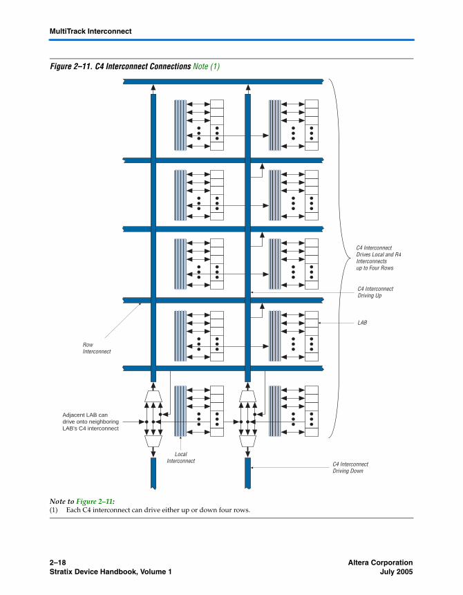
The C4 interconnects span four LABs, M512, or M4K blocks up or down from a source LAB. Every LAB has its own set of C4 interconnects to drive either up or down. Figure 2–11 shows the C4 interconnect connections from an LAB in a column. The C4 interconnects can drive and be driven by all types of architecture blocks, including DSP blocks, TriMatrix memory blocks, and vertical IOEs. For LAB interconnection, a primary LAB or its LAB neighbor can drive a given C4 interconnect. C4 interconnects can drive each other to extend their range as well as drive row interconnects for column-to-column connections.
LE 1
LE 2
LE 3
LE 4
LE 5
LE 6
LE 7
LE 8
LE 9
LE 10
LUT ChainRouting to
Adjacent LE
LocalInterconnect
Register ChainRouting to AdjacentLE's Register Input
Local InterconnectRouting Among LEsin the LAB
2–18 Altera CorporationStratix Device Handbook, Volume 1 July 2005
MultiTrack Interconnect
Figure 2–11. C4 Interconnect Connections Note (1)
Note to Figure 2–11:(1) Each C4 interconnect can drive either up or down four rows.
C4 InterconnectDrives Local and R4Interconnectsup to Four Rows
Adjacent LAB candrive onto neighboringLAB's C4 interconnect
C4 InterconnectDriving Up
C4 InterconnectDriving Down
LAB
RowInterconnect
LocalInterconnect

Altera Corporation 2–19July 2005 Stratix Device Handbook, Volume 1
Stratix Architecture
C8 interconnects span eight LABs, M512, or M4K blocks up or down from a source LAB. Every LAB has its own set of C8 interconnects to drive either up or down. C8 interconnect connections between the LABs in a column are similar to the C4 connections shown in Figure 2–11 with the exception that they connect to eight LABs above and below. The C8 interconnects can drive and be driven by all types of architecture blocks similar to C4 interconnects. C8 interconnects can drive each other to extend their range as well as R8 interconnects for column-to-column connections. C8 interconnects are faster than two C4 interconnects.
C16 column interconnects span a length of 16 LABs and provide the fastest resource for long column connections between LABs, TriMatrix memory blocks, DSP blocks, and IOEs. C16 interconnects can cross M-RAM blocks and also drive to row and column interconnects at every fourth LAB. C16 interconnects drive LAB local interconnects via C4 and R4 interconnects and do not drive LAB local interconnects directly.
All embedded blocks communicate with the logic array similar to LAB-to-LAB interfaces. Each block (i.e., TriMatrix memory and DSP blocks) connects to row and column interconnects and has local interconnect regions driven by row and column interconnects. These blocks also have direct link interconnects for fast connections to and from a neighboring LAB. All blocks are fed by the row LAB clocks, labclk[7..0].
2–20 Altera CorporationStratix Device Handbook, Volume 1 July 2005
MultiTrack Interconnect
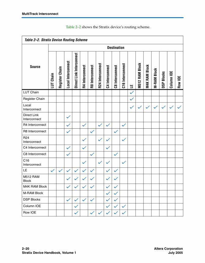
Table 2–2 shows the Stratix device’s routing scheme.
Table 2–2. Stratix Device Routing Scheme
Source
DestinationLU
T Ch
ain
Regi
ster
Cha
in
Loca
l Int
erco
nnec
t
Dire
ct L
ink
Inte
rcon
nect
R4 In
terc
onne
ct
R8 In
terc
onne
ct
R24
Inte
rcon
nect
C4 In
terc
onne
ct
C8 In
terc
onne
ct
C16
Inte
rcon
nect
LE M51
2 RA
M B
lock
M4K
RAM
Blo
ck
M-R
AM B
lock
DSP
Bloc
ks
Colu
mn
IOE
Row
IOE
LUT Chain v
Register Chain v
Local Interconnect v v v v v v v
Direct Link Interconnect v
R4 Interconnect v v v v v
R8 Interconnect v v v
R24 Interconnect v v v v
C4 Interconnect v v v
C8 Interconnect v v v
C16 Interconnect v v v v
LE v v v v v v v v
M512 RAM Block v v v v v v
M4K RAM Block v v v v v v
M-RAM Block v v
DSP Blocks v v v v v v
Column IOE v v v v
Row IOE v v v v v v

Altera Corporation 2–21July 2005 Stratix Device Handbook, Volume 1
Stratix Architecture
TriMatrix Memory
TriMatrix memory consists of three types of RAM blocks: M512, M4K, and M-RAM blocks. Although these memory blocks are different, they can all implement various types of memory with or without parity, including true dual-port, simple dual-port, and single-port RAM, ROM, and FIFO buffers. Table 2–3 shows the size and features of the different RAM blocks.
Table 2–3. TriMatrix Memory Features (Part 1 of 2)
Memory Feature M512 RAM Block (32 × 18 Bits)
M4K RAM Block (128 × 36 Bits)
M-RAM Block (4K × 144 Bits)
Maximum performance
(1) (1) (1)
True dual-port memory v v
Simple dual-port memory v v v
Single-port memory v v v
Shift register v v
ROM v v (2)
FIFO buffer v v v
Byte enable v v
Parity bits v v v
Mixed clock mode v v v
Memory initialization v v
Simple dual-port memory mixed width support
v v v
True dual-port memory mixed width support
v v
Power-up conditions Outputs cleared Outputs cleared Outputs unknown
Register clears Input and output registers
Input and output registers
Output registers
Mixed-port read-during-write
Unknown output/old data
Unknown output/old data
Unknown output

2–22 Altera CorporationStratix Device Handbook, Volume 1 July 2005
TriMatrix Memory
1 Violating the setup or hold time on the address registers could corrupt the memory contents. This applies to both read and write operations.
Memory Modes
TriMatrix memory blocks include input registers that synchronize writes and output registers to pipeline designs and improve system performance. M4K and M-RAM memory blocks offer a true dual-port mode to support any combination of two-port operations: two reads, two writes, or one read and one write at two different clock frequencies. Figure 2–12 shows true dual-port memory.
Figure 2–12. True Dual-Port Memory Configuration
Configurations 512 × 1256 × 2128 × 464 × 864 × 932 × 1632 × 18
4K × 12K × 21K × 4512 × 8512 × 9256 × 16256 × 18128 × 32128 × 36
64K × 864K × 932K × 1632K × 1816K × 3216K × 368K × 648K × 724K × 1284K × 144
Notes to Table 2–3:(1) See Table 4–36 for maximum performance information.(2) The M-RAM block does not support memory initializations. However, the
M-RAM block can emulate a ROM function using a dual-port RAM bock. The Stratix device must write to the dual-port memory once and then disable the write-enable ports afterwards.
Table 2–3. TriMatrix Memory Features (Part 2 of 2)
Memory Feature M512 RAM Block (32 × 18 Bits)
M4K RAM Block (128 × 36 Bits)
M-RAM Block (4K × 144 Bits)
dataA[ ]addressA[ ]wrenA
clockA
clockenA
qA[ ]aclrA
dataB[ ]addressB[ ]
wrenB
clockB clockenB
qB[ ]aclrB
A B
Altera Corporation 2–23July 2005 Stratix Device Handbook, Volume 1
Stratix Architecture
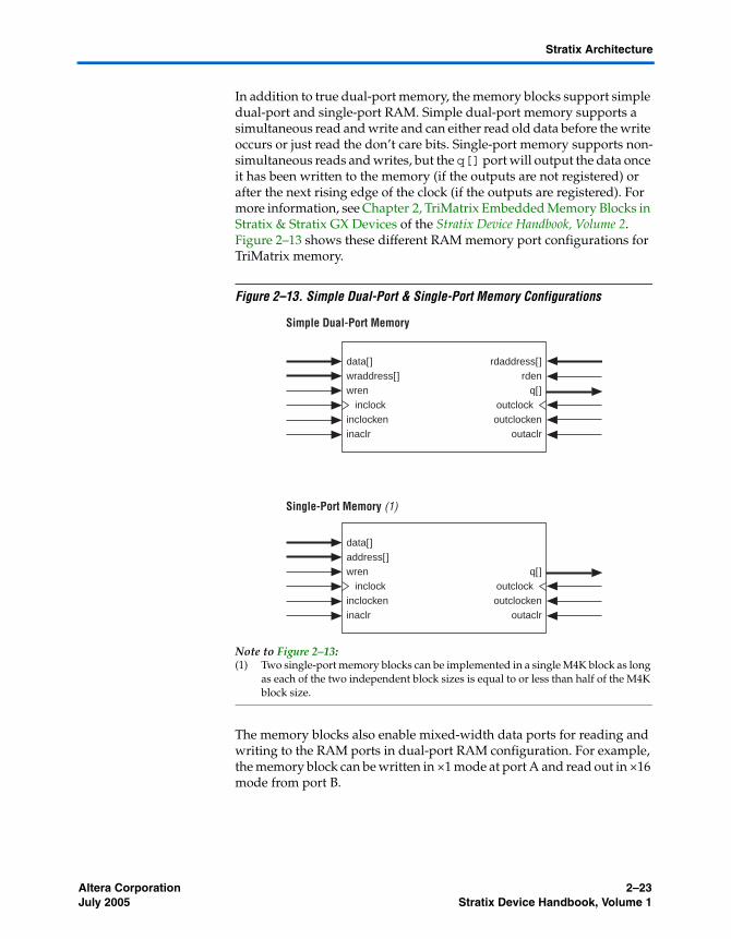
In addition to true dual-port memory, the memory blocks support simple dual-port and single-port RAM. Simple dual-port memory supports a simultaneous read and write and can either read old data before the write occurs or just read the don’t care bits. Single-port memory supports non-simultaneous reads and writes, but the q[] port will output the data once it has been written to the memory (if the outputs are not registered) or after the next rising edge of the clock (if the outputs are registered). For more information, see Chapter 2, TriMatrix Embedded Memory Blocks in Stratix & Stratix GX Devices of the Stratix Device Handbook, Volume 2. Figure 2–13 shows these different RAM memory port configurations for TriMatrix memory.
Figure 2–13. Simple Dual-Port & Single-Port Memory Configurations
Note to Figure 2–13:(1) Two single-port memory blocks can be implemented in a single M4K block as long
as each of the two independent block sizes is equal to or less than half of the M4K block size.
The memory blocks also enable mixed-width data ports for reading and writing to the RAM ports in dual-port RAM configuration. For example, the memory block can be written in ×1 mode at port A and read out in ×16 mode from port B.
data[ ]wraddress[ ]wren inclockinclockeninaclr
rdaddress[ ]rden
q[ ]outclock outclocken
outaclr
data[ ]address[ ]wren inclockinclockeninaclr
q[ ]outclock outclocken
outaclr
Single-Port Memory (1)
Simple Dual-Port Memory

2–24 Altera CorporationStratix Device Handbook, Volume 1 July 2005
TriMatrix Memory
TriMatrix memory architecture can implement pipelined RAM by registering both the input and output signals to the RAM block. All TriMatrix memory block inputs are registered providing synchronous write cycles. In synchronous operation, the memory block generates its own self-timed strobe write enable (WREN) signal derived from the global or regional clock. In contrast, a circuit using asynchronous RAM must generate the RAM WREN signal while ensuring its data and address signals meet setup and hold time specifications relative to the WREN signal. The output registers can be bypassed. Flow-through reading is possible in the simple dual-port mode of M512 and M4K RAM blocks by clocking the read enable and read address registers on the negative clock edge and bypassing the output registers.
Two single-port memory blocks can be implemented in a single M4K block as long as each of the two independent block sizes is equal to or less than half of the M4K block size.
The Quartus II software automatically implements larger memory by combining multiple TriMatrix memory blocks. For example, two 256 × 16-bit RAM blocks can be combined to form a 256 × 32-bit RAM block. Memory performance does not degrade for memory blocks using the maximum number of words available in one memory block. Logical memory blocks using less than the maximum number of words use physical blocks in parallel, eliminating any external control logic that would increase delays. To create a larger high-speed memory block, the Quartus II software automatically combines memory blocks with LE control logic.
Clear Signals
When applied to input registers, the asynchronous clear signal for the TriMatrix embedded memory immediately clears the input registers. However, the output of the memory block does not show the effects until the next clock edge. When applied to output registers, the asynchronous clear signal clears the output registers and the effects are seen immediately.
Parity Bit Support
The memory blocks support a parity bit for each byte. The parity bit, along with internal LE logic, can implement parity checking for error detection to ensure data integrity. You can also use parity-size data words to store user-specified control bits. In the M4K and M-RAM blocks, byte enables are also available for data input masking during write operations.
Altera Corporation 2–25July 2005 Stratix Device Handbook, Volume 1
Stratix Architecture
Shift Register Support
You can configure embedded memory blocks to implement shift registers for DSP applications such as pseudo-random number generators, multi-channel filtering, auto-correlation, and cross-correlation functions. These and other DSP applications require local data storage, traditionally implemented with standard flip-flops, which can quickly consume many logic cells and routing resources for large shift registers. A more efficient alternative is to use embedded memory as a shift register block, which saves logic cell and routing resources and provides a more efficient implementation with the dedicated circuitry.
The size of a w × m × n shift register is determined by the input data width (w), the length of the taps (m), and the number of taps (n). The size of a w × m × n shift register must be less than or equal to the maximum number of memory bits in the respective block: 576 bits for the M512 RAM block and 4,608 bits for the M4K RAM block. The total number of shift register outputs (number of taps n × width w) must be less than the maximum data width of the RAM block (18 for M512 blocks, 36 for M4K blocks). To create larger shift registers, the memory blocks are cascaded together.
Data is written into each address location at the falling edge of the clock and read from the address at the rising edge of the clock. The shift register mode logic automatically controls the positive and negative edge clocking to shift the data in one clock cycle. Figure 2–14 shows the TriMatrix memory block in the shift register mode.
2–26 Altera CorporationStratix Device Handbook, Volume 1 July 2005
TriMatrix Memory
Figure 2–14. Shift Register Memory Configuration
Memory Block Size
TriMatrix memory provides three different memory sizes for efficient application support. The large number of M512 blocks are ideal for designs with many shallow first-in first-out (FIFO) buffers. M4K blocks provide additional resources for channelized functions that do not require large amounts of storage. The M-RAM blocks provide a large single block of RAM ideal for data packet storage. The different-sized blocks allow Stratix devices to efficiently support variable-sized memory in designs.
The Quartus II software automatically partitions the user-defined memory into the embedded memory blocks using the most efficient size combinations. You can also manually assign the memory to a specific block size or a mixture of block sizes.
m-Bit Shift Registerw w
m-Bit Shift Register
m-Bit Shift Register
m-Bit Shift Register
w w
w w
w w
w × m × n Shift Register
n Numberof Taps

Altera Corporation 2–27July 2005 Stratix Device Handbook, Volume 1
Stratix Architecture
M512 RAM Block
The M512 RAM block is a simple dual-port memory block and is useful for implementing small FIFO buffers, DSP, and clock domain transfer applications. Each block contains 576 RAM bits (including parity bits). M512 RAM blocks can be configured in the following modes:
■ Simple dual-port RAM■ Single-port RAM■ FIFO■ ROM■ Shift register
When configured as RAM or ROM, you can use an initialization file to pre-load the memory contents.
The memory address depths and output widths can be configured as 512 × 1, 256 × 2, 128 × 4, 64 × 8 (64 × 9 bits with parity), and 32 × 16 (32 × 18 bits with parity). Mixed-width configurations are also possible, allowing different read and write widths. Table 2–4 summarizes the possible M512 RAM block configurations.
When the M512 RAM block is configured as a shift register block, a shift register of size up to 576 bits is possible.
The M512 RAM block can also be configured to support serializer and deserializer applications. By using the mixed-width support in combination with DDR I/O standards, the block can function as a SERDES to support low-speed serial I/O standards using global or regional clocks. See “I/O Structure” on page 2–104 for details on dedicated SERDES in Stratix devices.
Table 2–4. M512 RAM Block Configurations (Simple Dual-Port RAM)
Read PortWrite Port
512 × 1 256 × 2 128 × 4 64 × 8 32 × 16 64 × 9 32 × 18
512 × 1 v v v v v
256 × 2 v v v v v
128 × 4 v v v v
64 × 8 v v v
32 × 16 v v v v
64 × 9 v
32 × 18 v
2–28 Altera CorporationStratix Device Handbook, Volume 1 July 2005
TriMatrix Memory
M512 RAM blocks can have different clocks on its inputs and outputs. The wren, datain, and write address registers are all clocked together from one of the two clocks feeding the block. The read address, rden, and output registers can be clocked by either of the two clocks driving the block. This allows the RAM block to operate in read/write or input/output clock modes. Only the output register can be bypassed. The eight labclk signals or local interconnect can drive the inclock, outclock, wren, rden, inclr, and outclr signals. Because of the advanced interconnect between the LAB and M512 RAM blocks, LEs can also control the wren and rden signals and the RAM clock, clock enable, and asynchronous clear signals. Figure 2–15 shows the M512 RAM block control signal generation logic.
The RAM blocks within Stratix devices have local interconnects to allow LEs and interconnects to drive into RAM blocks. The M512 RAM block local interconnect is driven by the R4, R8, C4, C8, and direct link interconnects from adjacent LABs. The M512 RAM blocks can communicate with LABs on either the left or right side through these row interconnects or with LAB columns on the left or right side with the column interconnects. Up to 10 direct link input connections to the M512 RAM block are possible from the left adjacent LABs and another 10 possible from the right adjacent LAB. M512 RAM outputs can also connect to left and right LABs through 10 direct link interconnects. The M512 RAM block has equal opportunity for access and performance to and from LABs on either its left or right side. Figure 2–16 shows the M512 RAM block to logic array interface.

Altera Corporation 2–29July 2005 Stratix Device Handbook, Volume 1
Stratix Architecture
Figure 2–15. M512 RAM Block Control Signals
inclocken
outclockinclock
outclocken
rden
wren
DedicatedRow LABClocks
LocalInterconnect
LocalInterconnect
LocalInterconnect
LocalInterconnect
LocalInterconnect
LocalInterconnect
inclr
outclr
8
LocalInterconnect
LocalInterconnect

2–30 Altera CorporationStratix Device Handbook, Volume 1 July 2005
TriMatrix Memory
Figure 2–16. M512 RAM Block LAB Row Interface
M4K RAM Blocks
The M4K RAM block includes support for true dual-port RAM. The M4K RAM block is used to implement buffers for a wide variety of applications such as storing processor code, implementing lookup schemes, and implementing larger memory applications. Each block contains 4,608 RAM bits (including parity bits). M4K RAM blocks can be configured in the following modes:
■ True dual-port RAM■ Simple dual-port RAM■ Single-port RAM■ FIFO■ ROM■ Shift register
When configured as RAM or ROM, you can use an initialization file to pre-load the memory contents.
dataout
M512 RAMBlock
datain
Clocks
10
Direct link interconnectfrom adjacent LAB
Direct link interconnectto adjacent LAB
Direct link interconnectfrom adjacent LAB
Direct link interconnectto adjacent LAB
Small RAM Block LocalInterconnect Region
C4 and C8Interconnects R4 and R8
Interconnects
ControlSignals
address
LAB Row Clocks
2
8
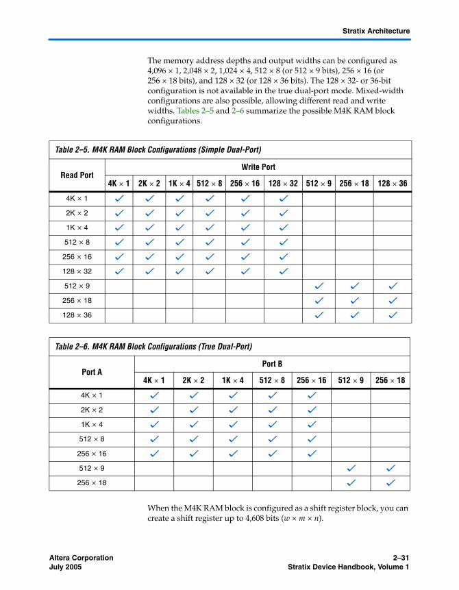
Altera Corporation 2–31July 2005 Stratix Device Handbook, Volume 1
Stratix Architecture
The memory address depths and output widths can be configured as 4,096 × 1, 2,048 × 2, 1,024 × 4, 512 × 8 (or 512 × 9 bits), 256 × 16 (or 256 × 18 bits), and 128 × 32 (or 128 × 36 bits). The 128 × 32- or 36-bit configuration is not available in the true dual-port mode. Mixed-width configurations are also possible, allowing different read and write widths. Tables 2–5 and 2–6 summarize the possible M4K RAM block configurations.
When the M4K RAM block is configured as a shift register block, you can create a shift register up to 4,608 bits (w × m × n).
Table 2–5. M4K RAM Block Configurations (Simple Dual-Port)
Read PortWrite Port
4K × 1 2K × 2 1K × 4 512 × 8 256 × 16 128 × 32 512 × 9 256 × 18 128 × 36
4K × 1 v v v v v v
2K × 2 v v v v v v
1K × 4 v v v v v v
512 × 8 v v v v v v
256 × 16 v v v v v v
128 × 32 v v v v v v
512 × 9 v v v
256 × 18 v v v
128 × 36 v v v
Table 2–6. M4K RAM Block Configurations (True Dual-Port)
Port APort B
4K × 1 2K × 2 1K × 4 512 × 8 256 × 16 512 × 9 256 × 18
4K × 1 v v v v v
2K × 2 v v v v v
1K × 4 v v v v v
512 × 8 v v v v v
256 × 16 v v v v v
512 × 9 v v
256 × 18 v v
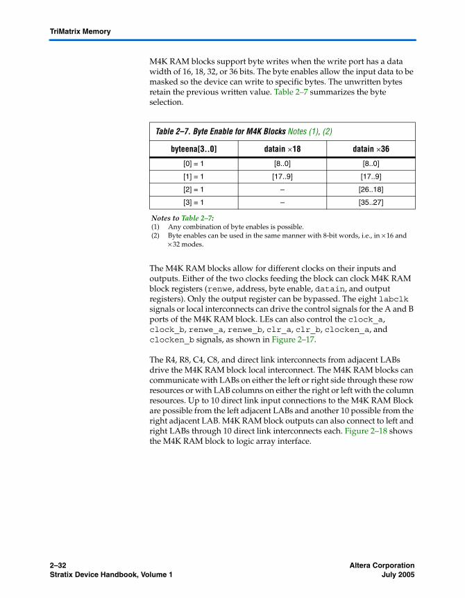
2–32 Altera CorporationStratix Device Handbook, Volume 1 July 2005
TriMatrix Memory
M4K RAM blocks support byte writes when the write port has a data width of 16, 18, 32, or 36 bits. The byte enables allow the input data to be masked so the device can write to specific bytes. The unwritten bytes retain the previous written value. Table 2–7 summarizes the byte selection.
The M4K RAM blocks allow for different clocks on their inputs and outputs. Either of the two clocks feeding the block can clock M4K RAM block registers (renwe, address, byte enable, datain, and output registers). Only the output register can be bypassed. The eight labclk signals or local interconnects can drive the control signals for the A and B ports of the M4K RAM block. LEs can also control the clock_a, clock_b, renwe_a, renwe_b, clr_a, clr_b, clocken_a, and clocken_b signals, as shown in Figure 2–17.
The R4, R8, C4, C8, and direct link interconnects from adjacent LABs drive the M4K RAM block local interconnect. The M4K RAM blocks can communicate with LABs on either the left or right side through these row resources or with LAB columns on either the right or left with the column resources. Up to 10 direct link input connections to the M4K RAM Block are possible from the left adjacent LABs and another 10 possible from the right adjacent LAB. M4K RAM block outputs can also connect to left and right LABs through 10 direct link interconnects each. Figure 2–18 shows the M4K RAM block to logic array interface.
Table 2–7. Byte Enable for M4K Blocks Notes (1), (2)
byteena[3..0] datain ×18 datain ×36
[0] = 1 [8..0] [8..0]
[1] = 1 [17..9] [17..9]
[2] = 1 – [26..18]
[3] = 1 – [35..27]
Notes to Table 2–7:(1) Any combination of byte enables is possible.(2) Byte enables can be used in the same manner with 8-bit words, i.e., in × 16 and
× 32 modes.

Altera Corporation 2–33July 2005 Stratix Device Handbook, Volume 1
Stratix Architecture
Figure 2–17. M4K RAM Block Control Signals
Figure 2–18. M4K RAM Block LAB Row Interface
clocken_a
renwe_aclock_a
alcr_a
alcr_b
renwe_b
DedicatedRow LABClocks
LocalInterconnect
LocalInterconnect
LocalInterconnect
LocalInterconnect
LocalInterconnect
clocken_b
clock_b
8
LocalInterconnect
LocalInterconnect
LocalInterconnect
LocalInterconnect
LocalInterconnect
dataout
M4K RAMBlock
datainaddress
10
Direct link interconnectfrom adjacent LAB
Direct link interconnectto adjacent LAB
Direct link interconnectfrom adjacent LAB
Direct link interconnectto adjacent LAB
M4K RAM Block LocalInterconnect Region
C4 and C8Interconnects R4 and R8
Interconnects
LAB Row Clocks
Clocks
Byte enable
ControlSignals
8
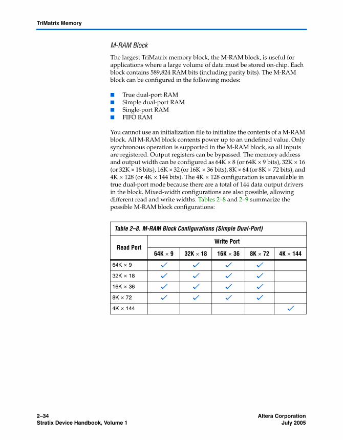
2–34 Altera CorporationStratix Device Handbook, Volume 1 July 2005
TriMatrix Memory
M-RAM Block
The largest TriMatrix memory block, the M-RAM block, is useful for applications where a large volume of data must be stored on-chip. Each block contains 589,824 RAM bits (including parity bits). The M-RAM block can be configured in the following modes:
■ True dual-port RAM■ Simple dual-port RAM■ Single-port RAM■ FIFO RAM
You cannot use an initialization file to initialize the contents of a M-RAM block. All M-RAM block contents power up to an undefined value. Only synchronous operation is supported in the M-RAM block, so all inputs are registered. Output registers can be bypassed. The memory address and output width can be configured as 64K × 8 (or 64K × 9 bits), 32K × 16 (or 32K × 18 bits), 16K × 32 (or 16K × 36 bits), 8K × 64 (or 8K × 72 bits), and 4K × 128 (or 4K × 144 bits). The 4K × 128 configuration is unavailable in true dual-port mode because there are a total of 144 data output drivers in the block. Mixed-width configurations are also possible, allowing different read and write widths. Tables 2–8 and 2–9 summarize the possible M-RAM block configurations:
Table 2–8. M-RAM Block Configurations (Simple Dual-Port)
Read PortWrite Port
64K × 9 32K × 18 16K × 36 8K × 72 4K × 144
64K × 9 v v v v
32K × 18 v v v v
16K × 36 v v v v
8K × 72 v v v v
4K × 144 v
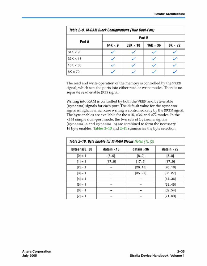
Altera Corporation 2–35July 2005 Stratix Device Handbook, Volume 1
Stratix Architecture
The read and write operation of the memory is controlled by the WREN signal, which sets the ports into either read or write modes. There is no separate read enable (RE) signal.
Writing into RAM is controlled by both the WREN and byte enable (byteena) signals for each port. The default value for the byteena signal is high, in which case writing is controlled only by the WREN signal. The byte enables are available for the ×18, ×36, and ×72 modes. In the ×144 simple dual-port mode, the two sets of byteena signals (byteena_a and byteena_b) are combined to form the necessary 16 byte enables. Tables 2–10 and 2–11 summarize the byte selection.
Table 2–9. M-RAM Block Configurations (True Dual-Port)
Port APort B
64K × 9 32K × 18 16K × 36 8K × 72
64K × 9 v v v v
32K × 18 v v v v
16K × 36 v v v v
8K × 72 v v v v
Table 2–10. Byte Enable for M-RAM Blocks Notes (1), (2)
byteena[3..0] datain ×18 datain ×36 datain ×72
[0] = 1 [8..0] [8..0] [8..0]
[1] = 1 [17..9] [17..9] [17..9]
[2] = 1 – [26..18] [26..18]
[3] = 1 – [35..27] [35..27]
[4] = 1 – – [44..36]
[5] = 1 – – [53..45]
[6] = 1 – – [62..54]
[7] = 1 – – [71..63]
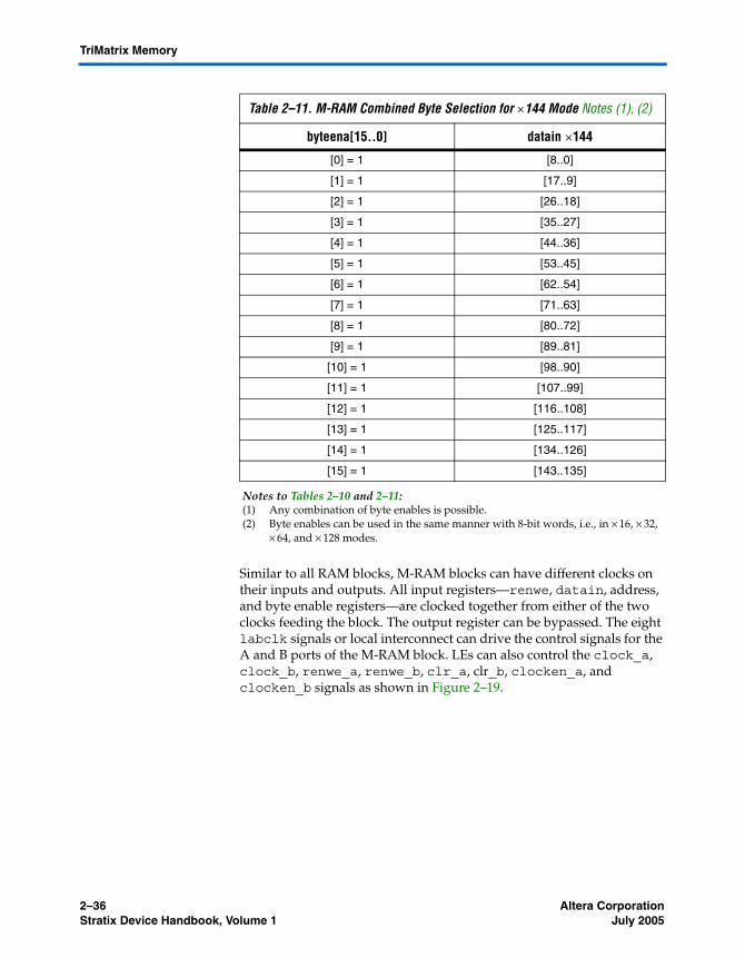
2–36 Altera CorporationStratix Device Handbook, Volume 1 July 2005
TriMatrix Memory
Similar to all RAM blocks, M-RAM blocks can have different clocks on their inputs and outputs. All input registers—renwe, datain, address, and byte enable registers—are clocked together from either of the two clocks feeding the block. The output register can be bypassed. The eight labclk signals or local interconnect can drive the control signals for the A and B ports of the M-RAM block. LEs can also control the clock_a, clock_b, renwe_a, renwe_b, clr_a, clr_b, clocken_a, and clocken_b signals as shown in Figure 2–19.
Table 2–11. M-RAM Combined Byte Selection for ×144 Mode Notes (1), (2)
byteena[15..0] datain ×144
[0] = 1 [8..0]
[1] = 1 [17..9]
[2] = 1 [26..18]
[3] = 1 [35..27]
[4] = 1 [44..36]
[5] = 1 [53..45]
[6] = 1 [62..54]
[7] = 1 [71..63]
[8] = 1 [80..72]
[9] = 1 [89..81]
[10] = 1 [98..90]
[11] = 1 [107..99]
[12] = 1 [116..108]
[13] = 1 [125..117]
[14] = 1 [134..126]
[15] = 1 [143..135]
Notes to Tables 2–10 and 2–11:(1) Any combination of byte enables is possible.(2) Byte enables can be used in the same manner with 8-bit words, i.e., in × 16, × 32,
× 64, and × 128 modes.

Altera Corporation 2–37July 2005 Stratix Device Handbook, Volume 1
Stratix Architecture
Figure 2–19. M-RAM Block Control Signals
One of the M-RAM block’s horizontal sides drive the address and control signal (clock, renwe, byteena, etc.) inputs. Typically, the horizontal side closest to the device perimeter contains the interfaces. The one exception is when two M-RAM blocks are paired next to each other. In this case, the side of the M-RAM block opposite the common side of the two blocks contains the input interface. The top and bottom sides of any M-RAM block contain data input and output interfaces to the logic array. The top side has 72 data inputs and 72 data outputs for port B, and the bottom side has another 72 data inputs and 72 data outputs for port A. Figure 2–20 shows an example floorplan for the EP1S60 device and the location of the M-RAM interfaces.
clocken_a
clock_bclock_a
clocken_b
aclr_a
aclr_b
DedicatedRow LABClocks
LocalInterconnect
LocalInterconnect
LocalInterconnect
LocalInterconnect renwe_a
renwe_b
8
LocalInterconnect
LocalInterconnect
LocalInterconnect
LocalInterconnect
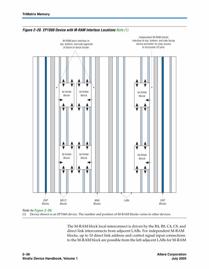
2–38 Altera CorporationStratix Device Handbook, Volume 1 July 2005
TriMatrix Memory
Figure 2–20. EP1S60 Device with M-RAM Interface Locations Note (1)
Note to Figure 2–20:(1) Device shown is an EP1S60 device. The number and position of M-RAM blocks varies in other devices.
The M-RAM block local interconnect is driven by the R4, R8, C4, C8, and direct link interconnects from adjacent LABs. For independent M-RAM blocks, up to 10 direct link address and control signal input connections to the M-RAM block are possible from the left adjacent LABs for M-RAM
M-RAMBlock
M-RAMBlock
DSPBlocks
DSPBlocks
M4KBlocks
M512Blocks
LABs
M-RAMBlock
M-RAMBlock
M-RAMBlock
M-RAMBlock
M-RAM pairs interface to top, bottom, and side opposite
of block-to-block border.
Independent M-RAM blocksinterface to top, bottom, and side facing
device perimeter for easy accessto horizontal I/O pins.

Altera Corporation 2–39July 2005 Stratix Device Handbook, Volume 1
Stratix Architecture
blocks facing to the left, and another 10 possible from the right adjacent LABs for M-RAM blocks facing to the right. For column interfacing, every M-RAM column unit connects to the right and left column lines, allowing each M-RAM column unit to communicate directly with three columns of LABs. Figures 2–21 through 2–23 show the interface between the M-RAM block and the logic array.

2–40 Altera CorporationStratix Device Handbook, Volume 1 July 2005
TriMatrix Memory
Figure 2–21. Left-Facing M-RAM to Interconnect Interface Notes (1), (2)
Notes to Figure 2–21:(1) Only R24 and C16 interconnects cross the M-RAM block boundaries.(2) The right-facing M-RAM block has interface blocks on the right side, but none on the left. B1 to B6 and A1 to A6
orientation is clipped across the vertical axis for right-facing M-RAM blocks.
M-RAM Block
Port B
Port A
Row Unit InterfaceAllows LAB Rows toDrive Address andControl Signals toM-RAM Block
Column Interface BlockAllows LAB Columns toDrive datain and dataout toand from M-RAM Block
LABs in RowM-RAM Boundary
LABs in ColumnM-RAM Boundary
M512 RAM Block Columns
Column Interface BlockDrives to and fromC4 and C8 Interconnects
LAB InterfaceBlocks
R11
R10
R9
R8
R7
R6
R5
R4
R3
R2
R1
A1 A2 A3 A4 A5 A6
B1 B2 B3 B4 B5 B6
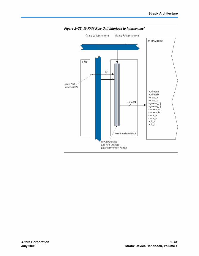
Altera Corporation 2–41July 2005 Stratix Device Handbook, Volume 1
Stratix Architecture
Figure 2–22. M-RAM Row Unit Interface to Interconnect
LAB
Row Interface Block
M-RAM Block
10
Up to 24
addressaaddressbrenwe_arenwe_bbyteenaA[ ]byteenaB[ ]clocken_aclocken_bclock_aclock_baclr_aaclr_b
M-RAM Block toLAB Row InterfaceBlock Interconnect Region
R4 and R8 InterconnectsC4 and C8 Interconnects
Direct LinkInterconnects

2–42 Altera CorporationStratix Device Handbook, Volume 1 July 2005
TriMatrix Memory
Figure 2–23. M-RAM Column Unit Interface to Interconnect
12 12
Column InterfaceBlock
M-RAM Block toLAB Row InterfaceBlock InterconnectRegion
datain dataout
LAB LABLAB
C4 and C8 Interconnects
M-RAM Block

Altera Corporation 2–43July 2005 Stratix Device Handbook, Volume 1
Stratix Architecture
Table 2–12 shows the input and output data signal connections for the column units (B1 to B6 and A1 to A6). It also shows the address and control signal input connections to the row units (R1 to R11).
Table 2–12. M-RAM Row & Column Interface Unit Signals
Unit Interface Block Input SIgnals Output Signals
R1 addressa[7..0]
R2 addressa[15..8]
R3 byte_enable_a[7..0]renwe_a
R4 -
R5 -
R6 clock_aclocken_aclock_b
clocken_b
R7 -
R8 -
R9 byte_enable_b[7..0]renwe_b
R10 addressb[15..8]
R11 addressb[7..0]
B1 datain_b[71..60] dataout_b[71..60]
B2 datain_b[59..48] dataout_b[59..48]
B3 datain_b[47..36] dataout_b[47..36]
B4 datain_b[35..24] dataout_b[35..24]
B5 datain_b[23..12] dataout_b[23..12]
B6 datain_b[11..0] dataout_b[11..0]
A1 datain_a[71..60] dataout_a[71..60]
A2 datain_a[59..48] dataout_a[59..48]
A3 datain_a[47..36] dataout_a[47..36]
A4 datain_a[35..24] dataout_a[35..24]
A5 datain_a[23..12] dataout_a[23..12]
A6 datain_a[11..0] dataout_a[11..0]

2–44 Altera CorporationStratix Device Handbook, Volume 1 July 2005
TriMatrix Memory
Independent Clock Mode
The memory blocks implement independent clock mode for true dual-port memory. In this mode, a separate clock is available for each port (ports A and B). Clock A controls all registers on the port A side, while clock B controls all registers on the port B side. Each port, A and B, also supports independent clock enables and asynchronous clear signals for port A and B registers. Figure 2–24 shows a TriMatrix memory block in independent clock mode.

Altera Corporation 2–45July 2005 Stratix Device Handbook, Volume 1
Stratix Architecture
Figure 2–24. Independent Clock Mode Notes (1), (2)
Notes to Figure 2–24(1) All registers shown have asynchronous clear ports.(2) Violating the setup or hold time on the address registers could corrupt the memory
contents. This applies to both read and write operations.
8D E
NA
Q
D EN
A
Q
D EN
A
Q
data
A[ ]
addr
ess A
[ ]
Mem
ory
Blo
ck25
6 ´
16 (
2)51
2 ´
81,
024
´ 4
2,04
8 ´
24,
096
´ 1
Dat
a In
Add
ress
A
Writ
e/R
ead
Ena
ble
Dat
a O
ut
Dat
a In
Add
ress
B
Writ
e/R
ead
Ena
ble
Dat
a O
ut
clke
n A
cloc
k A
D EN
A
Q
wre
n A
8 LA
B R
ow C
lock
s
q A[ ]
8da
taB[ ]
addr
ess B
[ ]
clke
n B
cloc
k B
wre
n B
q B[ ]
EN
A
AB
EN
ADQ
D EN
A
Qby
teen
a A[ ]
Byt
e E
nabl
e A
Byt
e E
nabl
e B
byte
ena B
[ ]
EN
ADQ
EN
ADQ
EN
ADQ
DQ
Writ
eP
ulse
Gen
erat
or
Writ
eP
ulse
Gen
erat
or
2–46 Altera CorporationStratix Device Handbook, Volume 1 July 2005
TriMatrix Memory
Input/Output Clock Mode
Input/output clock mode can be implemented for both the true and simple dual-port memory modes. On each of the two ports, A or B, one clock controls all registers for inputs into the memory block: data input, wren, and address. The other clock controls the block’s data output registers. Each memory block port, A or B, also supports independent clock enables and asynchronous clear signals for input and output registers. Figures 2–25 and 2–26 show the memory block in input/output clock mode.
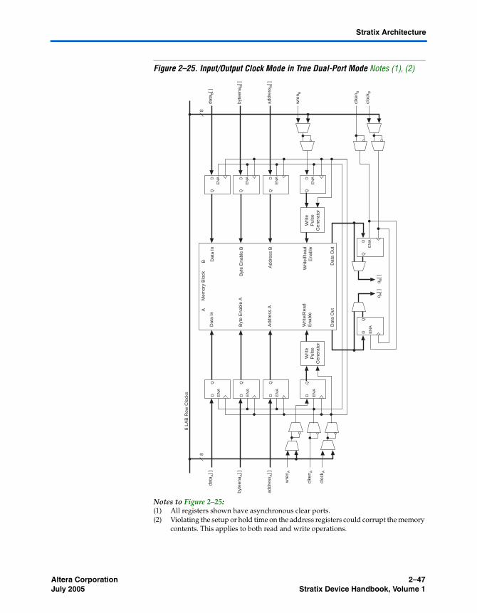
Altera Corporation 2–47July 2005 Stratix Device Handbook, Volume 1
Stratix Architecture
Figure 2–25. Input/Output Clock Mode in True Dual-Port Mode Notes (1), (2)
Notes to Figure 2–25:(1) All registers shown have asynchronous clear ports.(2) Violating the setup or hold time on the address registers could corrupt the memory
contents. This applies to both read and write operations.
8
D EN
A
Q
D EN
A
Q
D EN
A
Q
data
A[ ]
addr
ess A
[ ]
Mem
ory
Blo
ck25
6 ×
16 (2
)51
2 ×
81,
024
× 4
2,04
8 ×
24,
096
× 1
Dat
a In
Add
ress
A
Writ
e/R
ead
Ena
ble
Dat
a O
ut
Dat
a In
Add
ress
B
Writ
e/R
ead
Ena
ble
Dat
a O
ut
clke
n A
cloc
k A
D EN
A
Q
wre
n A
8 LA
B R
ow C
lock
s
q A[ ]
8
data
B[ ]
addr
ess B
[ ]
clke
n B
cloc
k B
wre
n B
q B[ ]
EN
A
AB
EN
ADQ
EN
ADQ
EN
ADQ
DQ
D EN
A
Qby
teen
a A[ ]
Byt
e E
nabl
e A
Byt
e E
nabl
e B
byte
ena B
[ ]
EN
ADQ
Writ
eP
ulse
Gen
erat
or
Writ
eP
ulse
Gen
erat
or

2–48 Altera CorporationStratix Device Handbook, Volume 1 July 2005
TriMatrix Memory
Figure 2–26. Input/Output Clock Mode in Simple Dual-Port Mode Notes (1), (2)
Notes to Figure 2–26:(1) All registers shown except the rden register have asynchronous clear ports.(2) Violating the setup or hold time on the address registers could corrupt the memory contents. This applies to both
read and write operations.
8
DENA
Q
D
ENA
Q
D
ENA
Q
D
ENA
Q
DENA
Q
data[ ]
DENA
Qwraddress[ ]
address[ ]
Memory Block256 ´ 16
512 ´ 81,024 ´ 42,048 ´ 24,096 ´ 1
Data In
Read Address
Write Address
Write Enable
Read Enable
Data Out
outclken
inclken
wrclock
rdclock
wren
rden
8 LAB Row Clocks
To MultiTrackInterconnect
DENA
Qbyteena[ ] Byte Enable
WritePulse
Generator

Altera Corporation 2–49July 2005 Stratix Device Handbook, Volume 1
Stratix Architecture
Read/Write Clock Mode
The memory blocks implement read/write clock mode for simple dual-port memory. You can use up to two clocks in this mode. The write clock controls the block’s data inputs, wraddress, and wren. The read clock controls the data output, rdaddress, and rden. The memory blocks support independent clock enables for each clock and asynchronous clear signals for the read- and write-side registers. Figure 2–27 shows a memory block in read/write clock mode.
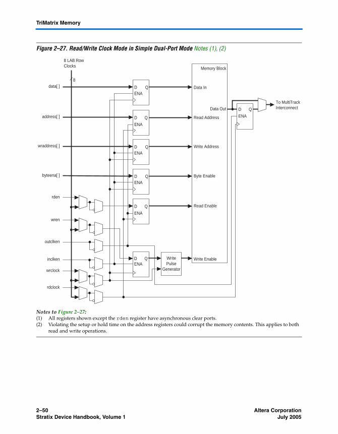
2–50 Altera CorporationStratix Device Handbook, Volume 1 July 2005
TriMatrix Memory
Figure 2–27. Read/Write Clock Mode in Simple Dual-Port Mode Notes (1), (2)
Notes to Figure 2–27:(1) All registers shown except the rden register have asynchronous clear ports.(2) Violating the setup or hold time on the address registers could corrupt the memory contents. This applies to both
read and write operations.
8
DENA
Q
D
ENA
Q
D
ENA
Q
D
ENA
Q
DENA
Q
data[ ]
DENA
Qwraddress[ ]
address[ ]
Memory Block256 × 16
512 × 81,024 × 42,048 × 24,096 × 1
Data In
Read Address
Write Address
Write Enable
Read Enable
Data Out
outclken
inclken
wrclock
rdclock
wren
rden
8 LAB RowClocks
To MultiTrackInterconnect
DENA
Qbyteena[ ] Byte Enable
WritePulse
Generator
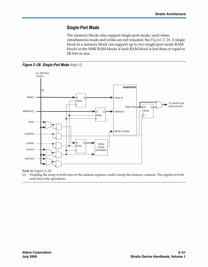
Altera Corporation 2–51July 2005 Stratix Device Handbook, Volume 1
Stratix Architecture
Single-Port Mode
The memory blocks also support single-port mode, used when simultaneous reads and writes are not required. See Figure 2–28. A single block in a memory block can support up to two single-port mode RAM blocks in the M4K RAM blocks if each RAM block is less than or equal to 2K bits in size.
Figure 2–28. Single-Port Mode Note (1)
Note to Figure 2–28:(1) Violating the setup or hold time on the address registers could corrupt the memory contents. This applies to both
read and write operations.
8
DENA
Q
D
ENA
Q
D
ENA
Q
DENA
Q
data[ ]
address[ ]
RAM/ROM256 × 16
512 × 81,024 × 42,048 × 24,096 × 1
Data In
Address
Write Enable
Data Out
outclken
inclken
inclock
outclock
WritePulse
Generator
wren
8 LAB RowClocks
To MultiTrackInterconnect

2–52 Altera CorporationStratix Device Handbook, Volume 1 July 2005
Digital Signal Processing Block
Digital Signal Processing Block
The most commonly used DSP functions are finite impulse response (FIR) filters, complex FIR filters, infinite impulse response (IIR) filters, fast Fourier transform (FFT) functions, direct cosine transform (DCT) functions, and correlators. All of these blocks have the same fundamental building block: the multiplier. Additionally, some applications need specialized operations such as multiply-add and multiply-accumulate operations. Stratix devices provide DSP blocks to meet the arithmetic requirements of these functions.
Each Stratix device has two columns of DSP blocks to efficiently implement DSP functions faster than LE-based implementations. Larger Stratix devices have more DSP blocks per column (see Table 2–13). Each DSP block can be configured to support up to:
■ Eight 9 × 9-bit multipliers■ Four 18 × 18-bit multipliers■ One 36 × 36-bit multiplier
As indicated, the Stratix DSP block can support one 36 × 36-bit multiplier in a single DSP block. This is true for any matched sign multiplications (either unsigned by unsigned or signed by signed), but the capabilities for dynamic and mixed sign multiplications are handled differently. The following list provides the largest functions that can fit into a single DSP block.
■ 36 × 36-bit unsigned by unsigned multiplication■ 36 × 36-bit signed by signed multiplication■ 35 × 36-bit unsigned by signed multiplication■ 36 × 35-bit signed by unsigned multiplication■ 36 × 35-bit signed by dynamic sign multiplication■ 35 × 36-bit dynamic sign by signed multiplication■ 35 × 36-bit unsigned by dynamic sign multiplication■ 36 × 35-bit dynamic sign by unsigned multiplication■ 35 × 35-bit dynamic sign multiplication when the sign controls for
each operand are different ■ 36 × 36-bit dynamic sign multiplication when the same sign control
is used for both operands
1 This list only shows functions that can fit into a single DSP block. Multiple DSP blocks can support larger multiplication functions.
Figure 2–29 shows one of the columns with surrounding LAB rows.
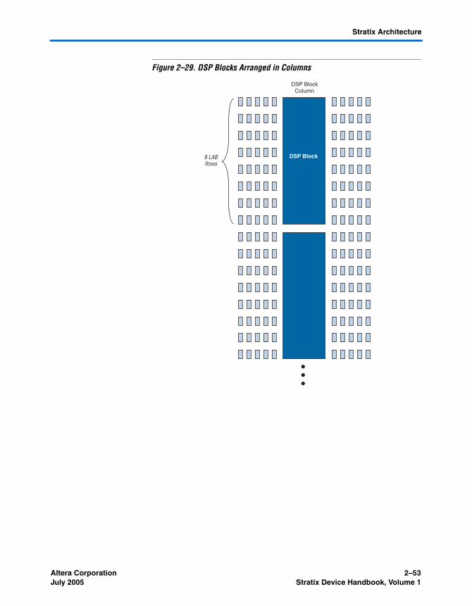
Altera Corporation 2–53July 2005 Stratix Device Handbook, Volume 1
Stratix Architecture
Figure 2–29. DSP Blocks Arranged in Columns
DSP BlockColumn
8 LABRows
DSP Block
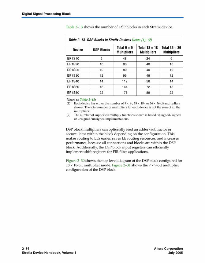
2–54 Altera CorporationStratix Device Handbook, Volume 1 July 2005
Digital Signal Processing Block
Table 2–13 shows the number of DSP blocks in each Stratix device.
DSP block multipliers can optionally feed an adder/subtractor or accumulator within the block depending on the configuration. This makes routing to LEs easier, saves LE routing resources, and increases performance, because all connections and blocks are within the DSP block. Additionally, the DSP block input registers can efficiently implement shift registers for FIR filter applications.
Figure 2–30 shows the top-level diagram of the DSP block configured for 18 × 18-bit multiplier mode. Figure 2–31 shows the 9 × 9-bit multiplier configuration of the DSP block.
Table 2–13. DSP Blocks in Stratix Devices Notes (1), (2)
Device DSP Blocks Total 9 × 9 Multipliers
Total 18 × 18 Multipliers
Total 36 × 36 Multipliers
EP1S10 6 48 24 6
EP1S20 10 80 40 10
EP1S25 10 80 40 10
EP1S30 12 96 48 12
EP1S40 14 112 56 14
EP1S60 18 144 72 18
EP1S80 22 176 88 22
Notes to Table 2–13:(1) Each device has either the number of 9 × 9-, 18 × 18-, or 36 × 36-bit multipliers
shown. The total number of multipliers for each device is not the sum of all the multipliers.
(2) The number of supported multiply functions shown is based on signed/signed or unsigned/unsigned implementations.

Altera Corporation 2–55July 2005 Stratix Device Handbook, Volume 1
Stratix Architecture
Figure 2–30. DSP Block Diagram for 18 × 18-Bit Configuration
Adder/Subtractor/
Accumulator2
Adder/Subtractor/
Accumulator1
Summation
Optional PipelineRegister Stage
Multiplier Stage
Output SelectionMultiplexer
Optional Output Register Stage
CLRN
D Q
ENA
CLRN
D Q
ENA
CLRN
D Q
ENA
CLRN
D Q
ENA
CLRN
D Q
ENA
CLRN
D Q
ENA
CLRN
D Q
ENA
CLRN
D Q
ENA
CLRN
D Q
ENA
CLRN
D Q
ENA
CLRN
D Q
ENA
CLRN
D Q
ENA
Optional Serial Shift RegisterInputs from Previous DSP Block
Optional Stage Configurableas Accumulator or DynamicAdder/Subtractor
Summation Stagefor Adding FourMultipliers Together
Optional Input RegisterStage with Parallel Input orShift Register Configuration
Optional Serial Shift Register Outputs to Next DSP Blockin the Column
to MultiTrackInterconnect

2–56 Altera CorporationStratix Device Handbook, Volume 1 July 2005
Digital Signal Processing Block
Figure 2–31. DSP Block Diagram for 9 × 9-Bit Configuration
CLRN
D QENA
CLRN
D QENA
CLRN
D QENA
Adder/Subtractor/
1a
Summation
Summation
CLRN
D QENA
CLRN
D QENA
CLRN
D QENA
CLRN
D QENA
CLRN
D QENA
CLRN
D QENA
CLRN
D QENA
Adder/Subtractor/
1b
CLRN
D QENA
CLRN
D QENA
CLRN
D QENA
CLRN
D QENA
CLRN
D QENA
CLRN
D QENA
Adder/Subtractor/
2a
CLRN
D QENA
CLRN
D QENA
CLRN
D QENA
CLRN
D QENA
CLRN
D QENA
CLRN
D QENA
Adder/Subtractor/
2b
CLRN
D QENA
CLRN
D QENA
CLRN
D QENA
OutputSelection
Multiplexer
To MultiTrackInterconnect

Altera Corporation 2–57July 2005 Stratix Device Handbook, Volume 1
Stratix Architecture
The DSP block consists of the following elements:
■ Multiplier block■ Adder/output block
Multiplier Block
The DSP block multiplier block consists of the input registers, a multiplier, and pipeline register for pipelining multiply-accumulate and multiply-add/subtract functions as shown in Figure 2–32.
Figure 2–32. Multiplier Sub-Block within Stratix DSP Block
Note to Figure 2–32:(1) These signals can be unregistered or registered once to match data path pipelines if required.
CLRN
D Q
ENA
Data A
Data B
Resultto Adderblocks
shiftout B shiftout A
shiftin Ashiftin B
aclr[3..0]clock[3..0]
ena[3..0]
OptionalMultiply-Accumulateand Multiply-AddPipeline
sign_a (1)sign_b (1)
CLRN
D Q
ENA
CLRN
D Q
ENA

2–58 Altera CorporationStratix Device Handbook, Volume 1 July 2005
Digital Signal Processing Block
Input Registers
A bank of optional input registers is located at the input of each multiplier and multiplicand inputs to the multiplier. When these registers are configured for parallel data inputs, they are driven by regular routing resources. You can use a clock signal, asynchronous clear signal, and a clock enable signal to independently control each set of A and B inputs for each multiplier in the DSP block. You select these control signals from a set of four different clock[3..0], aclr[3..0], and ena[3..0] signals that drive the entire DSP block.
You can also configure the input registers for a shift register application. In this case, the input registers feed the multiplier and drive two dedicated shift output lines: shiftoutA and shiftoutB. The shift outputs of one multiplier block directly feed the adjacent multiplier block in the same DSP block (or the next DSP block) as shown in Figure 2–33, to form a shift register chain. This chain can terminate in any block, that is, you can create any length of shift register chain up to 224 registers. You can use the input shift registers for FIR filter applications. One set of shift inputs can provide data for a filter, and the other are coefficients that are optionally loaded in serial or parallel. When implementing 9 × 9- and 18 × 18-bit multipliers, you do not need to implement external shift registers in LAB LEs. You implement all the filter circuitry within the DSP block and its routing resources, saving LE and general routing resources for general logic. External registers are needed for shift register inputs when using 36 × 36-bit multipliers.

Altera Corporation 2–59July 2005 Stratix Device Handbook, Volume 1
Stratix Architecture
Figure 2–33. Multiplier Sub-Blocks Using Input Shift Register Connections Note (1)
Note to Figure 2–33:(1) Either Data A or Data B input can be set to a parallel input for constant coefficient
multiplication.
CLRN
D Q
ENA
Data A
Data B
A[n] × B[n]
CLRN
D Q
ENA
CLRN
D Q
ENA
CLRN
D Q
ENA
Data AData B
A[n Ð 1] × B[n Ð 1]
CLRN
D Q
ENA
CLRN
D Q
ENA
CLRN
D Q
ENA
Data AData B
A[n Ð 2] × B[n Ð 2]
CLRN
D Q
ENA
CLRN
D Q
ENA

2–60 Altera CorporationStratix Device Handbook, Volume 1 July 2005
Digital Signal Processing Block
Table 2–14 shows the summary of input register modes for the DSP block.
Multiplier
The multiplier supports 9 × 9-, 18 × 18-, or 36 × 36-bit multiplication. Each DSP block supports eight possible 9 × 9-bit or smaller multipliers. There are four multiplier blocks available for multipliers larger than 9 × 9 bits but smaller than 18 × 18 bits. There is one multiplier block available for multipliers larger than 18 × 18 bits but smaller than or equal to 36 × 36 bits. The ability to have several small multipliers is useful in applications such as video processing. Large multipliers greater than 18 × 18 bits are useful for applications such as the mantissa multiplication of a single-precision floating-point number.
The multiplier operands can be signed or unsigned numbers, where the result is signed if either input is signed as shown in Table 2–15. The sign_a and sign_b signals provide dynamic control of each operand’s representation: a logic 1 indicates the operand is a signed number, a logic 0 indicates the operand is an unsigned number. These sign signals affect all multipliers and adders within a single DSP block and you can register them to match the data path pipeline. The multipliers are full precision (that is, 18 bits for the 18-bit multiply, 36-bits for the 36-bit multiply, and so on) regardless of whether sign_a or sign_b set the operands as signed or unsigned numbers.
Table 2–14. Input Register Modes
Register Input Mode 9 × 9 18 × 18 36 × 36
Parallel input v v v
Shift register input v v
Table 2–15. Multiplier Signed Representation
Data A Data B Result
Unsigned Unsigned Unsigned
Unsigned Signed Signed
Signed Unsigned Signed
Signed Signed Signed

Altera Corporation 2–61July 2005 Stratix Device Handbook, Volume 1
Stratix Architecture
Pipeline/Post Multiply Register
The output of 9 × 9- or 18 × 18-bit multipliers can optionally feed a register to pipeline multiply-accumulate and multiply-add/subtract functions. For 36 × 36-bit multipliers, this register will pipeline the multiplier function.
Adder/Output Blocks
The result of the multiplier sub-blocks are sent to the adder/output block which consist of an adder/subtractor/accumulator unit, summation unit, output select multiplexer, and output registers. The results are used to configure the adder/output block as a pure output, accumulator, a simple two-multiplier adder, four-multiplier adder, or final stage of the 36-bit multiplier. You can configure the adder/output block to use output registers in any mode, and must use output registers for the accumulator. The system cannot use adder/output blocks independently of the multiplier. Figure 2–34 shows the adder and output stages.

2–62 Altera CorporationStratix Device Handbook, Volume 1 July 2005
Digital Signal Processing Block
Figure 2–34. Adder/Output Blocks Note (1)
Notes to Figure 2–34:(1) Adder/output block shown in Figure 2–34 is in 18 × 18-bit mode. In 9 × 9-bit mode, there are four adder/subtractor
blocks and two summation blocks.(2) These signals are either not registered, registered once, or registered twice to match the data path pipeline.
Adder/Subtractor/
Accumulator1
Summation
Result A
Result B
Result C
Result D
addnsub1 (2)
accum_sload0 (2)
addnsub3 (2)
signa (2)
signb (2)
accum_sload1 (2)
Accumulator Feedback
Accumulator Feedback
overflow0
Adder/Subtractor/
Accumulator2
Output SelectionMultiplexer
Output Register Block
overflow1
Altera Corporation 2–63July 2005 Stratix Device Handbook, Volume 1
Stratix Architecture
Adder/Subtractor/Accumulator
The adder/subtractor/accumulator is the first level of the adder/output block and can be used as an accumulator or as an adder/subtractor.
Adder/SubtractorEach adder/subtractor/accumulator block can perform addition or subtraction using the addnsub independent control signal for each first-level adder in 18 × 18-bit mode. There are two addnsub[1..0] signals available in a DSP block for any configuration. For 9 × 9-bit mode, one addnsub[1..0] signal controls the top two one-level adders and another addnsub[1..0] signal controls the bottom two one-level adders. A high addnsub signal indicates addition, and a low signal indicates subtraction. The addnsub control signal can be unregistered or registered once or twice when feeding the adder blocks to match data path pipelines.
The signa and signb signals serve the same function as the multiplier block signa and signb signals. The only difference is that these signals can be registered up to two times. These signals are tied to the same signa and signb signals from the multiplier and must be connected to the same clocks and control signals.
AccumulatorWhen configured for accumulation, the adder/output block output feeds back to the accumulator as shown in Figure 2–34. The accum_sload[1..0] signal synchronously loads the multiplier result to the accumulator output. This signal can be unregistered or registered once or twice. Additionally, the overflow signal indicates the accumulator has overflowed or underflowed in accumulation mode. This signal is always registered and must be externally latched in LEs if the design requires a latched overflow signal.
Summation
The output of the adder/subtractor/accumulator block feeds to an optional summation block. This block sums the outputs of the DSP block multipliers. In 9 × 9-bit mode, there are two summation blocks providing the sums of two sets of four 9 × 9-bit multipliers. In 18 × 18-bit mode, there is one summation providing the sum of one set of four 18 × 18-bit multipliers.
2–64 Altera CorporationStratix Device Handbook, Volume 1 July 2005
Digital Signal Processing Block
Output Selection Multiplexer
The outputs from the various elements of the adder/output block are routed through an output selection multiplexer. Based on the DSP block operational mode and user settings, the multiplexer selects whether the output from the multiplier, the adder/subtractor/accumulator, or summation block feeds to the output.
Output Registers
Optional output registers for the DSP block outputs are controlled by four sets of control signals: clock[3..0], aclr[3..0], and ena[3..0]. Output registers can be used in any mode.
Modes of Operation
The adder, subtractor, and accumulate functions of a DSP block have four modes of operation:
■ Simple multiplier■ Multiply-accumulator■ Two-multipliers adder■ Four-multipliers adder
1 Each DSP block can only support one mode. Mixed modes in the same DSP block is not supported.
Simple Multiplier Mode
In simple multiplier mode, the DSP block drives the multiplier sub-block result directly to the output with or without an output register. Up to four 18 × 18-bit multipliers or eight 9 × 9-bit multipliers can drive their results directly out of one DSP block. See Figure 2–35.

Altera Corporation 2–65July 2005 Stratix Device Handbook, Volume 1
Stratix Architecture
Figure 2–35. Simple Multiplier Mode
Note to Figure 2–35:(1) These signals are not registered or registered once to match the data path pipeline.
DSP blocks can also implement one 36 × 36-bit multiplier in multiplier mode. DSP blocks use four 18 × 18-bit multipliers combined with dedicated adder and internal shift circuitry to achieve 36-bit multiplication. The input shift register feature is not available for the 36 × 36-bit multiplier. In 36 × 36-bit mode, the device can use the register that is normally a multiplier-result-output register as a pipeline stage for the 36 × 36-bit multiplier. Figure 2–36 shows the 36 × 36-bit multiply mode.
CLRN
D Q
ENA
Data A
Data B
Data Out
shiftout B shiftout A
shiftin Ashiftin B
aclrclock
ena
signa (1)signb (1)
CLRN
D Q
ENA
CLRN
D Q
ENA
CLRN
D Q
ENA
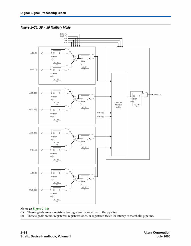
2–66 Altera CorporationStratix Device Handbook, Volume 1 July 2005
Digital Signal Processing Block
Figure 2–36. 36 × 36 Multiply Mode
Notes to Figure 2–36:(1) These signals are not registered or registered once to match the pipeline.(2) These signals are not registered, registered once, or registered twice for latency to match the pipeline.
CLRN
D Q
ENA
A[17..0]
A[17..0]
B[17..0]
B[17..0]
A[35..18]
A[35..18]
B[35..18]
B[35..18]
aclrclock
ena
signa (1)signb (1)
CLRN
D Q
ENA
CLRN
D Q
ENA
CLRN
D Q
ENA
CLRN
D Q
ENA
CLRN
D Q
ENA
CLRN
D Q
ENA
CLRN
D Q
ENA
CLRN
D Q
ENA
CLRN
D Q
ENA
CLRN
D Q
ENA
CLRN
D Q
ENA
CLRN
D Q
ENA
Data Out
36 × 36Multiplier
Adder
signa (2)
signb (2)

Altera Corporation 2–67July 2005 Stratix Device Handbook, Volume 1
Stratix Architecture
Multiply-Accumulator Mode
In multiply-accumulator mode (see Figure 2–37), the DSP block drives multiplied results to the adder/subtractor/accumulator block configured as an accumulator. You can implement one or two multiply-accumulators up to 18 × 18 bits in one DSP block. The first and third multiplier sub-blocks are unused in this mode, because only one multiplier can feed one of two accumulators. The multiply-accumulator output can be up to 52 bits—a maximum of a 36-bit result with 16 bits of accumulation. The accum_sload and overflow signals are only available in this mode. The addnsub signal can set the accumulator for decimation and the overflow signal indicates underflow condition.
Figure 2–37. Multiply-Accumulate Mode
Notes to Figure 2–37:(1) These signals are not registered or registered once to match the data path pipeline.(2) These signals are not registered, registered once, or registered twice for latency to match the data path pipeline.
Two-Multipliers Adder Mode
The two-multipliers adder mode uses the adder/subtractor/accumulator block to add or subtract the outputs of the multiplier block, which is useful for applications such as FFT functions and complex FIR filters. A
CLRN
D Q
ENA
CLRN
D Q
ENA
Data A
Data B
Data Out
overflow
Shiftout B Shiftout A
Shiftin AShiftin B
aclrclock
ena
signa (1)signb (1)
CLRN
D Q
ENA
CLRN
D Q
ENA
Accumulator
addnsub (2)signa (2)signb (2)
accum_sload (2)
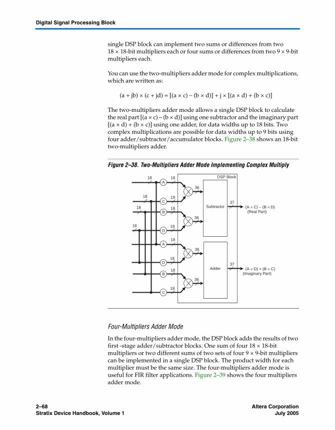
2–68 Altera CorporationStratix Device Handbook, Volume 1 July 2005
Digital Signal Processing Block
single DSP block can implement two sums or differences from two 18 × 18-bit multipliers each or four sums or differences from two 9 × 9-bit multipliers each.
You can use the two-multipliers adder mode for complex multiplications, which are written as:
(a + jb) × (c + jd) = [(a × c) – (b × d)] + j × [(a × d) + (b × c)]
The two-multipliers adder mode allows a single DSP block to calculate the real part [(a × c) – (b × d)] using one subtractor and the imaginary part [(a × d) + (b × c)] using one adder, for data widths up to 18 bits. Two complex multiplications are possible for data widths up to 9 bits using four adder/subtractor/accumulator blocks. Figure 2–38 shows an 18-bit two-multipliers adder.
Figure 2–38. Two-Multipliers Adder Mode Implementing Complex Multiply
Four-Multipliers Adder Mode
In the four-multipliers adder mode, the DSP block adds the results of two first -stage adder/subtractor blocks. One sum of four 18 × 18-bit multipliers or two different sums of two sets of four 9 × 9-bit multipliers can be implemented in a single DSP block. The product width for each multiplier must be the same size. The four-multipliers adder mode is useful for FIR filter applications. Figure 2–39 shows the four multipliers adder mode.
Subtractor
36
36
18
18
18
37
A18
(A × C) − (B × D)(Real Part)
Adder
36
36
18
18
37
A
18
18
18
(A × D) + (B × C)(Imaginary Part)
18
18
18
DSP Block
C
B
D
D
B
C

Altera Corporation 2–69July 2005 Stratix Device Handbook, Volume 1
Stratix Architecture
Figure 2–39. Four-Multipliers Adder Mode
Notes to Figure 2–39:(1) These signals are not registered or registered once to match the data path pipeline.(2) These signals are not registered, registered once, or registered twice for latency to match the data path pipeline.
CLRN
D Q
ENA
Data A
Data B
shiftin Ashiftin B
aclrclock
ena
signa (1)signb (1)
CLRN
D Q
ENA
CLRN
D Q
ENA
CLRN
D Q
ENA
Data A
Data B
CLRN
D Q
ENA
CLRN
D Q
ENA
Adder/Subtractor
CLRN
D Q
ENA
Data A
Data B
CLRN
D Q
ENA
CLRN
D Q
ENA
CLRN
D Q
ENA
Data A
Data B
shiftout B shiftout A
CLRN
D Q
ENA
CLRN
D Q
ENA
Adder/Subtractor
addnsub1 (2)signa (2)signb (2) CLRN
D Q
ENA
Data Out
addnsub3 (2)
Summation

2–70 Altera CorporationStratix Device Handbook, Volume 1 July 2005
Digital Signal Processing Block
For FIR filters, the DSP block combines the four-multipliers adder mode with the shift register inputs. One set of shift inputs contains the filter data, while the other holds the coefficients loaded in serial or parallel. The input shift register eliminates the need for shift registers external to the DSP block (i.e., implemented in LEs). This architecture simplifies filter design since the DSP block implements all of the filter circuitry.
One DSP block can implement an entire 18-bit FIR filter with up to four taps. For FIR filters larger than four taps, DSP blocks can be cascaded with additional adder stages implemented in LEs.
Table 2–16 shows the different number of multipliers possible in each DSP block mode according to size. These modes allow the DSP blocks to implement numerous applications for DSP including FFTs, complex FIR, FIR, and 2D FIR filters, equalizers, IIR, correlators, matrix multiplication and many other functions.
DSP Block Interface
Stratix device DSP block outputs can cascade down within the same DSP block column. Dedicated connections between DSP blocks provide fast connections between the shift register inputs to cascade the shift register chains. You can cascade DSP blocks for 9 × 9- or 18 × 18-bit FIR filters larger than four taps, with additional adder stages implemented in LEs. If the DSP block is configured as 36 × 36 bits, the adder, subtractor, or accumulator stages are implemented in LEs. Each DSP block can route the shift register chain out of the block to cascade two full columns of DSP blocks.
Table 2–16. Multiplier Size & Configurations per DSP block
DSP Block Mode 9 × 9 18 × 18 36 × 36 (1)
Multiplier Eight multipliers with eight product outputs
Four multipliers with four product outputs
One multiplier with one product output
Multiply-accumulator Two multiply and accumulate (52 bits)
Two multiply and accumulate (52 bits)
–
Two-multipliers adder Four sums of two multiplier products each
Two sums of two multiplier products each
–
Four-multipliers adder Two sums of four multiplier products each
One sum of four multiplier products each
–
Note to Table 2–16:(1) The number of supported multiply functions shown is based on signed/signed or unsigned/unsigned
implementations.
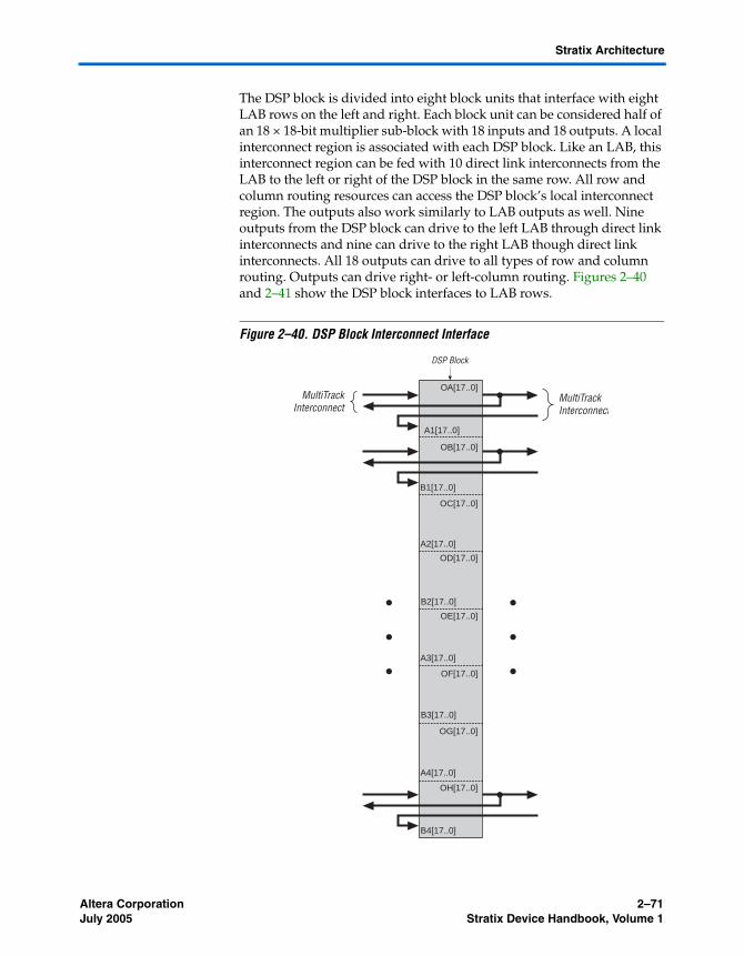
Altera Corporation 2–71July 2005 Stratix Device Handbook, Volume 1
Stratix Architecture
The DSP block is divided into eight block units that interface with eight LAB rows on the left and right. Each block unit can be considered half of an 18 × 18-bit multiplier sub-block with 18 inputs and 18 outputs. A local interconnect region is associated with each DSP block. Like an LAB, this interconnect region can be fed with 10 direct link interconnects from the LAB to the left or right of the DSP block in the same row. All row and column routing resources can access the DSP block’s local interconnect region. The outputs also work similarly to LAB outputs as well. Nine outputs from the DSP block can drive to the left LAB through direct link interconnects and nine can drive to the right LAB though direct link interconnects. All 18 outputs can drive to all types of row and column routing. Outputs can drive right- or left-column routing. Figures 2–40 and 2–41 show the DSP block interfaces to LAB rows.
Figure 2–40. DSP Block Interconnect Interface
A1[17..0]
B1[17..0]
A2[17..0]
B2[17..0]
A3[17..0]
B3[17..0]
A4[17..0]
B4[17..0]
OA[17..0]
OB[17..0]
OC[17..0]
OD[17..0]
OE[17..0]
OF[17..0]
OG[17..0]
OH[17..0]
DSP Block
MultiTrackInterconnect
MultiTrackInterconnect

2–72 Altera CorporationStratix Device Handbook, Volume 1 July 2005
Digital Signal Processing Block
Figure 2–41. DSP Block Interface to Interconnect
A bus of 18 control signals feeds the entire DSP block. These signals include clock[0..3] clocks, aclr[0..3] asynchronous clears, ena[1..4] clock enables, signa, signb signed/unsigned control signals, addnsub1 and addnsub3 addition and subtraction control signals, and accum_sload[0..1] accumulator synchronous loads. The
LAB LAB
Row InterfaceBlock
DSP BlockRow Structure
10
[17..0][17..0]
DSP Block toLAB Row InterfaceBlock Interconnect Region
18 Inputs per Row 18 Outputs per Row
R4 and R8 Interconnects
C4 and C8 Interconnects
Direct Link Interconnectfrom Adjacent LAB
Nine Direct Link Outputsto Adjacent LABs
Direct Link Interconnectfrom Adjacent LAB
18
18
18
Control3
9 9
10
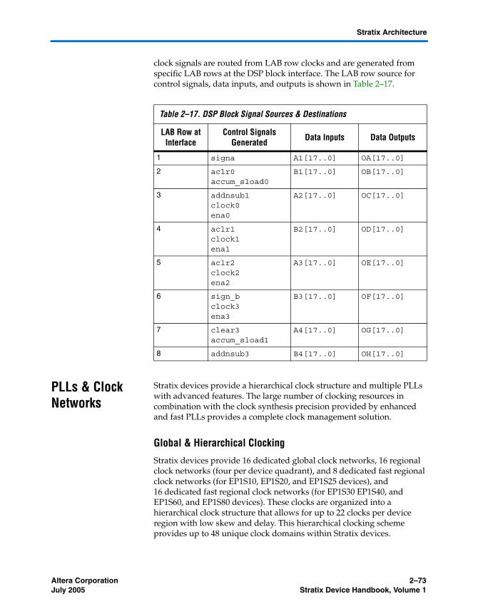
Altera Corporation 2–73July 2005 Stratix Device Handbook, Volume 1
Stratix Architecture
clock signals are routed from LAB row clocks and are generated from specific LAB rows at the DSP block interface. The LAB row source for control signals, data inputs, and outputs is shown in Table 2–17.
PLLs & Clock Networks
Stratix devices provide a hierarchical clock structure and multiple PLLs with advanced features. The large number of clocking resources in combination with the clock synthesis precision provided by enhanced and fast PLLs provides a complete clock management solution.
Global & Hierarchical Clocking
Stratix devices provide 16 dedicated global clock networks, 16 regional clock networks (four per device quadrant), and 8 dedicated fast regional clock networks (for EP1S10, EP1S20, and EP1S25 devices), and 16 dedicated fast regional clock networks (for EP1S30 EP1S40, and EP1S60, and EP1S80 devices). These clocks are organized into a hierarchical clock structure that allows for up to 22 clocks per device region with low skew and delay. This hierarchical clocking scheme provides up to 48 unique clock domains within Stratix devices.
Table 2–17. DSP Block Signal Sources & Destinations
LAB Row at Interface
Control Signals Generated Data Inputs Data Outputs
1 signa A1[17..0] OA[17..0]
2 aclr0accum_sload0
B1[17..0] OB[17..0]
3 addnsub1clock0ena0
A2[17..0] OC[17..0]
4 aclr1clock1ena1
B2[17..0] OD[17..0]
5 aclr2clock2ena2
A3[17..0] OE[17..0]
6 sign_bclock3ena3
B3[17..0] OF[17..0]
7 clear3accum_sload1
A4[17..0] OG[17..0]
8 addnsub3 B4[17..0] OH[17..0]

2–74 Altera CorporationStratix Device Handbook, Volume 1 July 2005
PLLs & Clock Networks
There are 16 dedicated clock pins (CLK[15..0]) to drive either the global or regional clock networks. Four clock pins drive each side of the device, as shown in Figure 2–42. Enhanced and fast PLL outputs can also drive the global and regional clock networks.
Global Clock Network
These clocks drive throughout the entire device, feeding all device quadrants. The global clock networks can be used as clock sources for all resources within the device—IOEs, LEs, DSP blocks, and all memory blocks. These resources can also be used for control signals, such as clock enables and synchronous or asynchronous clears fed from the external pin. The global clock networks can also be driven by internal logic for internally generated global clocks and asynchronous clears, clock enables, or other control signals with large fanout. Figure 2–42 shows the 16 dedicated CLK pins driving global clock networks.
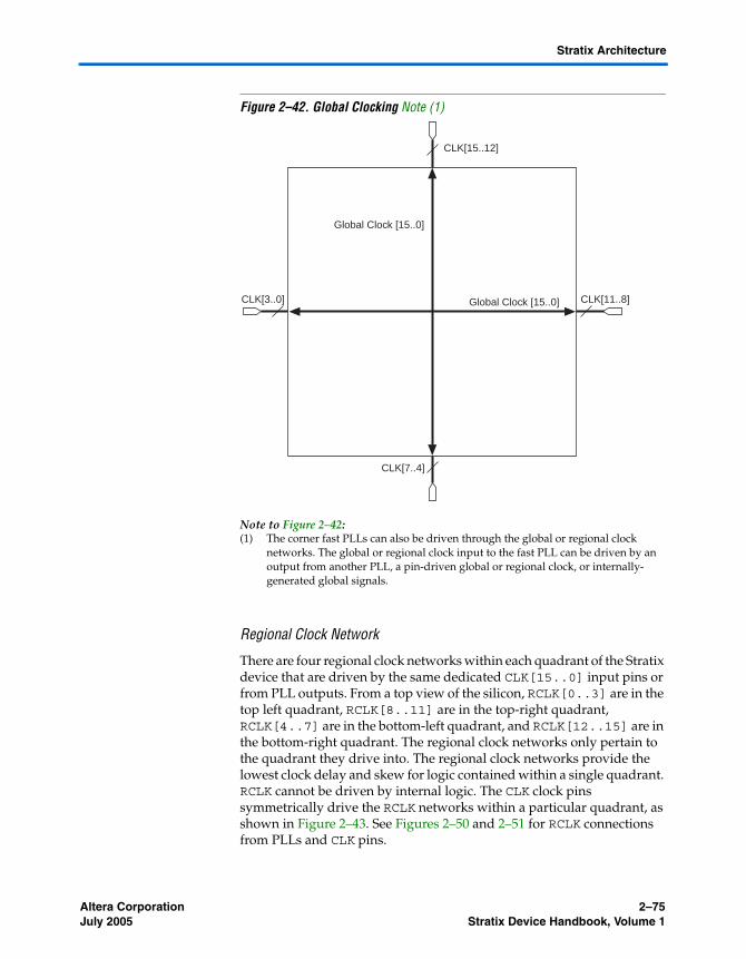
Altera Corporation 2–75July 2005 Stratix Device Handbook, Volume 1
Stratix Architecture
Figure 2–42. Global Clocking Note (1)
Note to Figure 2–42:(1) The corner fast PLLs can also be driven through the global or regional clock
networks. The global or regional clock input to the fast PLL can be driven by an output from another PLL, a pin-driven global or regional clock, or internally-generated global signals.
Regional Clock Network
There are four regional clock networks within each quadrant of the Stratix device that are driven by the same dedicated CLK[15..0] input pins or from PLL outputs. From a top view of the silicon, RCLK[0..3] are in the top left quadrant, RCLK[8..11] are in the top-right quadrant, RCLK[4..7] are in the bottom-left quadrant, and RCLK[12..15] are in the bottom-right quadrant. The regional clock networks only pertain to the quadrant they drive into. The regional clock networks provide the lowest clock delay and skew for logic contained within a single quadrant. RCLK cannot be driven by internal logic. The CLK clock pins symmetrically drive the RCLK networks within a particular quadrant, as shown in Figure 2–43. See Figures 2–50 and 2–51 for RCLK connections from PLLs and CLK pins.
Global Clock [15..0]
CLK[15..12]
CLK[3..0]
CLK[7..4]
CLK[11..8] Global Clock [15..0]

2–76 Altera CorporationStratix Device Handbook, Volume 1 July 2005
PLLs & Clock Networks
Figure 2–43. Regional Clocks
Fast Regional Clock Network
In EP1S25, EP1S20, and EP1S10 devices, there are two fast regional clock networks, FCLK[1..0], within each quadrant, fed by input pins that can connect to fast regional clock networks (see Figure 2–44). In EP1S30 and larger devices, there are two fast regional clock networks within each half-quadrant (see Figure 2–45). Dual-purpose FCLK pins drive the fast clock networks. All devices have eight FCLK pins to drive fast regional clock networks. Any I/O pin can drive a clock or control signal onto any fast regional clock network with the addition of a delay. This signal is driven via the I/O interconnect. The fast regional clock networks can also be driven from internal logic elements.
RCLK[1..0]
RCLK[4..5]
RCLK[6..7] RCLK[12..13]
RCLK[2..3] RCLK[11..10]
RCLK[14..15]
RCLK[9..8]
CLK[15..12]
CLK[3..0]
CLK[7..4]
CLK[11..8]
Regional Clocks Only Drive a Device Quadrant from Specified CLK Pins or PLLs within that Quadrant

Altera Corporation 2–77July 2005 Stratix Device Handbook, Volume 1
Stratix Architecture
Figure 2–44. EP1S25, EP1S20 & EP1S10 Device Fast Clock Pin Connections to Fast Regional Clocks
Notes to Figure 2–44:(1) This is a set of two multiplexers.(2) In addition to the FCLK pin inputs, there is also an input from the I/O interconnect.
FCLK[1..0]
FCLK[1..0]
FCLK[1..0]
FCLK[1..0]
FCLK[1..0] FCLK[7..6]
FCLK[5..4]FCLK[3..2]
2 2
2 2
2 2
2 2
(1), (2)
(1), (2)
(1), (2)
(1), (2)

2–78 Altera CorporationStratix Device Handbook, Volume 1 July 2005
PLLs & Clock Networks
Figure 2–45. EP1S30 Device Fast Regional Clock Pin Connections to Fast Regional Clocks
Notes to Figure 2–45:(1) This is a set of two multiplexers.(2) In addition to the FCLK pin inputs, there is also an input from the I/O interconnect.
Combined Resources
Within each region, there are 22 distinct dedicated clocking resources consisting of 16 global clock lines, four regional clock lines, and two fast regional clock lines. Multiplexers are used with these clocks to form eight bit busses to drive LAB row clocks, column IOE clocks, or row IOE clocks. Another multiplexer is used at the LAB level to select two of the eight row clocks to feed the LE registers within the LAB. See Figure 2–46.
fclk[1..0]
FCLK4FCLK5FCLK2FCLK3
FCLK6FCLK7FCLK0FCLK1
(1), (2)
(1), (2) (1), (2)
(1), (2)
(1), (2)
(1), (2) (1), (2)
(1), (2)

Altera Corporation 2–79July 2005 Stratix Device Handbook, Volume 1
Stratix Architecture
Figure 2–46. Regional Clock Bus
IOE clocks have horizontal and vertical block regions that are clocked by eight I/O clock signals chosen from the 22 quadrant or half-quadrant clock resources. Figures 2–47 and 2–48 show the quadrant and half-quadrant relationship to the I/O clock regions, respectively. The vertical regions (column pins) have less clock delay than the horizontal regions (row pins).
Clock [21..0]
Vertical I/O CellIO_CLK[7..0]
Lab Row Clock [7..0]
Horizontal I/OCell IO_CLK[7..0]
Global Clock Network [15..0]
Fast Regional Clock Network [1..0]
Regional Clock Network [3..0]
Clocks Availableto a Quadrant
or Half-Quadrant

2–80 Altera CorporationStratix Device Handbook, Volume 1 July 2005
PLLs & Clock Networks
Figure 2–47. EP1S10, EP1S20 & EP1S25 Device I/O Clock Groups
IO_CLKC[7..0]
IO_CLKF[7..0] IO_CLKE[7..0]
IO_CLKA[7..0] IO_CLKB[7..0]
IO_CLKD[7..0]
IO_CLKH[7..0]
IO_CLKG[7..0]
8
8
22 Clocks inthe Quadrant
22 Clocks inthe Quadrant
22 Clocks inthe Quadrant
22 Clocks inthe Quadrant
8
8
8
8
8 8I/O Clock Regions
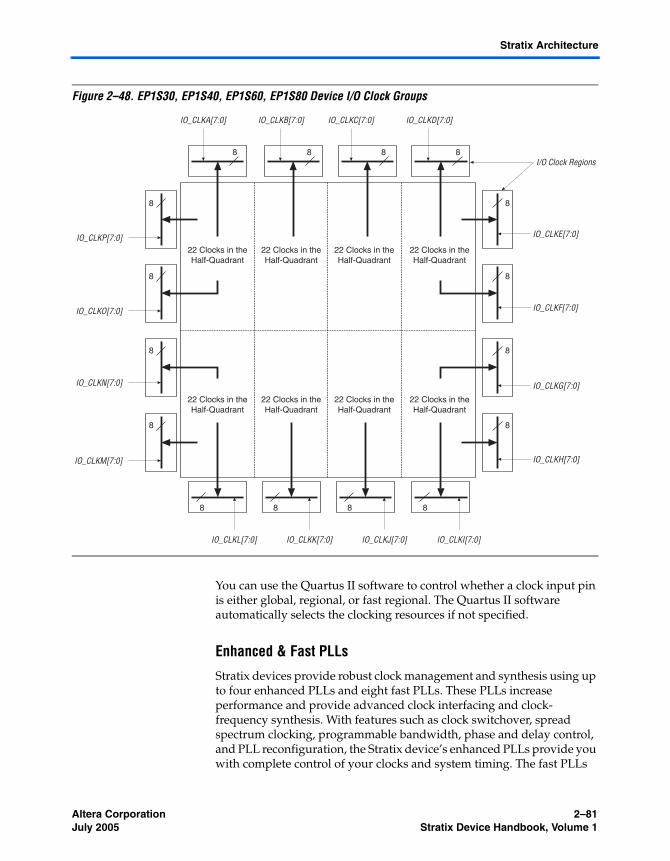
Altera Corporation 2–81July 2005 Stratix Device Handbook, Volume 1
Stratix Architecture
Figure 2–48. EP1S30, EP1S40, EP1S60, EP1S80 Device I/O Clock Groups
You can use the Quartus II software to control whether a clock input pin is either global, regional, or fast regional. The Quartus II software automatically selects the clocking resources if not specified.
Enhanced & Fast PLLs
Stratix devices provide robust clock management and synthesis using up to four enhanced PLLs and eight fast PLLs. These PLLs increase performance and provide advanced clock interfacing and clock-frequency synthesis. With features such as clock switchover, spread spectrum clocking, programmable bandwidth, phase and delay control, and PLL reconfiguration, the Stratix device’s enhanced PLLs provide you with complete control of your clocks and system timing. The fast PLLs
IO_CLKJ[7:0] IO_CLKI[7:0]
IO_CLKA[7:0] IO_CLKB[7:0]
8
22 Clocks in theHalf-Quadrant
22 Clocks in theHalf-Quadrant
22 Clocks in theHalf-Quadrant
22 Clocks in theHalf-Quadrant
22 Clocks in theHalf-Quadrant
22 Clocks in theHalf-Quadrant
22 Clocks in theHalf-Quadrant
22 Clocks in theHalf-Quadrant
8 8 8
I/O Clock Regions
IO_CLKL[7:0] IO_CLKK[7:0]
IO_CLKC[7:0] IO_CLKD[7:0]
8 8 8 8
8
8
8
8
8
8
8
8
IO_CLKE[7:0]
IO_CLKF[7:0]
IO_CLKG[7:0]
IO_CLKH[7:0]
IO_CLKN[7:0]
IO_CLKM[7:0]
IO_CLKP[7:0]
IO_CLKO[7:0]

2–82 Altera CorporationStratix Device Handbook, Volume 1 July 2005
PLLs & Clock Networks
provide general purpose clocking with multiplication and phase shifting as well as high-speed outputs for high-speed differential I/O support. Enhanced and fast PLLs work together with the Stratix high-speed I/O and advanced clock architecture to provide significant improvements in system performance and bandwidth.
The Quartus II software enables the PLLs and their features without requiring any external devices. Table 2–18 shows the PLLs available for each Stratix device.
Table 2–18. Stratix Device PLL Availability
DeviceFast PLLs Enhanced PLLs
1 2 3 4 7 8 9 10 5(1) 6(1) 11(2) 12(2)
EP1S10 v v v v v v
EP1S20 v v v v v v
EP1S25 v v v v v v
EP1S30 v v v v v (3) v (3) v (3) v (3) v v
EP1S40 v v v v v (3) v (3) v (3) v (3) v v v(3) v(3)
EP1S60 v v v v v v v v v v v v
EP1S80 v v v v v v v v v v v v
Notes to Table 2–18:(1) PLLs 5 and 6 each have eight single-ended outputs or four differential outputs.(2) PLLs 11 and 12 each have one single-ended output.(3) EP1S30 and EP1S40 devices do not support these PLLs in the 780-pin FineLine BGA® package.

Altera Corporation 2–83July 2005 Stratix Device Handbook, Volume 1
Stratix Architecture
Table 2–19 shows the enhanced PLL and fast PLL features in Stratix devices.
Table 2–19. Stratix PLL Features
Feature Enhanced PLL Fast PLL
Clock multiplication and division m/(n × post-scale counter) (1) m/(post-scale counter) (2)
Phase shift Down to 156.25-ps increments (3), (4) Down to 125-ps increments (3), (4)
Delay shift 250-ps increments for ±3 ns
Clock switchover v
PLL reconfiguration v
Programmable bandwidth v
Spread spectrum clocking v
Programmable duty cycle v v
Number of internal clock outputs 6 3 (5)
Number of external clock outputs Four differential/eight singled-ended or one single-ended (6)
(7)
Number of feedback clock inputs 2 (8)
Notes to Table 2–19:(1) For enhanced PLLs, m, n, range from 1 to 512 and post-scale counters g, l, e range from 1 to 1024 with 50% duty
cycle. With a non-50% duty cycle the post-scale counters g, l, e range from 1 to 512.(2) For fast PLLs, m and post-scale counters range from 1 to 32.(3) The smallest phase shift is determined by the voltage controlled oscillator (VCO) period divided by 8.(4) For degree increments, Stratix devices can shift all output frequencies in increments of at least 45° . Smaller degree
increments are possible depending on the frequency and divide parameters.(5) PLLs 7, 8, 9, and 10 have two output ports per PLL. PLLs 1, 2, 3, and 4 have three output ports per PLL.(6) Every Stratix device has two enhanced PLLs (PLLs 5 and 6) with either eight single-ended outputs or four
differential outputs each. Two additional enhanced PLLs (PLLs 11 and 12) in EP1S80, EP1S60, and EP1S40 devices each have one single-ended output. Devices in the 780 pin FineLine BGA packages do not support PLLs 11 and 12.
(7) Fast PLLs can drive to any I/O pin as an external clock. For high-speed differential I/O pins, the device uses a data channel to generate txclkout.
(8) Every Stratix device has two enhanced PLLs with one single-ended or differential external feedback input per PLL.

2–84 Altera CorporationStratix Device Handbook, Volume 1 July 2005
PLLs & Clock Networks
Figure 2–49 shows a top-level diagram of the Stratix device and PLL floorplan.
Figure 2–49. PLL Locations
FPLL7CLK FPLL10CLK
FPLL9CLK
CLK[8..11]
FPLL8CLK
CLK[3..0]
7
1
2
8
10
4
3
9
115
126
CLK[7..4]
CLK[15..12]
PLLs

Altera Corporation 2–85July 2005 Stratix Device Handbook, Volume 1
Stratix Architecture
Figure 2–50 shows the global and regional clocking from the PLL outputs and the CLK pins.
Figure 2–50. Global & Regional Clock Connections from Side Pins & Fast PLL Outputs Note (1), (2)
Notes to Figure 2–50:(1) PLLs 1 to 4 and 7 to 10 are fast PLLs. PLLs 5, 6, 11, and 12 are enhanced PLLs.(2) The global or regional clocks in a fast PLL’s quadrant can drive the fast PLL input. A pin or other PLL must drive
the global or regional source. The source cannot be driven by internally generated logic before driving the fast PLL.
Figure 2–51 shows the global and regional clocking from enhanced PLL outputs and top CLK pins.
2
CLK0CLK1
CLK2CLK3
G0
FPLL7CLK
G1G2
G3RCLK0
RCLK1
RCLK4
RCLK5
G10G11
G8G9
RCLK9RCLK8
RCLK15
RCLK14GlobalClocks
RegionalClocks
PLL 7
l0
l1
g0
PLL 1
PLL 2
FPLL8CLK
PLL 8
2
CLK10
CLK11
CLK8
CLK9
FPLL10CLK
PLL 10
PLL 4
PLL 3
FPLL9CLK
PLL 9
RegionalClocks
l0
l1
g0
l0
l1
g0
l0
l1
g0
l0
l1
g0
l0
l1
g0
l0
l1
g0
l0
l1
g0

2–86 Altera CorporationStratix Device Handbook, Volume 1 July 2005
PLLs & Clock Networks
Figure 2–51. Global & Regional Clock Connections from Top Clock Pins & Enhanced PLL Outputs Note (1)
Notes to Figure 2–51:(1) PLLs 1 to 4 and 7 to 10 are fast PLLs. PLLs 5, 6, 11, and 12 are enhanced PLLs.(2) CLK4, CLK6, CLK12, and CLK14 feed the corresponding PLL’s inclk0 port.(3) CLK5, CLK7, CLK13, and CLK15 feed the corresponding PLL’s inclk1 port.(4) The EP1S40 device in the 780-pin FineLine BGA package does not support PLLs 11 and 12.
G12G13G14G15
RCLK10RCLK11
RCLK2RCLK3
G7
G6G5G4
RCLK13
RCLK12RCLK7RCLK6
PLL 12
L0 L1 G0 G1 G2 G3
CLK7CLK6
CLK5CLK4
PLL 6
G0 G1 G2 G3 L0 L1
PLL 11
L0 L1 G0 G1 G2 G3
CLK13CLK12
CLK14
CLK15
PLL 5
G0 G1 G2 G3 L0 L1
E[0..3]
PLL12_OUT
PLL6_OUT[3..0]
PLL11_OUT
PLL5_OUT[3..0]
PLL5_FB
PLL6_FB
GlobalClocks
RegionalClocks
RegionalClocks
(1)
(2)
(1)
(2)
(2)
(2)(1)
(1)

Altera Corporation 2–87July 2005 Stratix Device Handbook, Volume 1
Stratix Architecture
Enhanced PLLs
Stratix devices contain up to four enhanced PLLs with advanced clock management features. Figure 2–52 shows a diagram of the enhanced PLL.
Figure 2–52. Stratix Enhanced PLL
Notes to Figure 2–52:(1) External feedback is available in PLLs 5 and 6.(2) This single-ended external output is available from the g0 counter for PLLs 11 and 12.(3) These four counters and external outputs are available in PLLs 5 and 6.(4) This connection is only available on EP1S40 and larger Stratix devices. For example, PLLs 5 and 11 are adjacent and
PLLs 6 and 12 are adjacent. The EP1S40 device in the 780-pin FineLine BGA package does not support PLLs 11 and 12.
/n ChargePump VCO /g0
/g1
/g2
/e0
8
4
GlobalClocks
/e1
/e2
I/O Buffers (3)
/e3 Δt
Δt
Δt
Δt
Δt
Δt
Δt
Δt
Lock Detect To I/O buffers or generalrouting
INCLK0
INCLK1
FBIN
PFD
/g3
/l1
/l0
From Adjacent PLL
/m
SpreadSpectrum
I/O buffers (2)(1)
LoopFilter
& Filter
Programmable Time Delay on Each PLL Port
Post-ScaleCounters
ClockSwitch-Over
Circuitry Phase FrequencyDetector
VCO Phase SelectionSelectable at EachPLL Output Port
VCO Phase SelectionAffecting All Outputs
Δt
Δt
Δt
Δt
RegionalClocks
4

2–88 Altera CorporationStratix Device Handbook, Volume 1 July 2005
PLLs & Clock Networks
Clock Multiplication & Division
Each Stratix device enhanced PLL provides clock synthesis for PLL output ports using m/(n × post-scale counter) scaling factors. The input clock is divided by a pre-scale divider, n, and is then multiplied by the m feedback factor. The control loop drives the VCO to match fIN × (m/n). Each output port has a unique post-scale counter that divides down the high-frequency VCO. For multiple PLL outputs with different frequencies, the VCO is set to the least common multiple of the output frequencies that meets its frequency specifications. Then, the post-scale dividers scale down the output frequency for each output port. For example, if output frequencies required from one PLL are 33 and 66 MHz, set the VCO to 330 MHz (the least common multiple in the VCO’s range). There is one pre-scale counter, n, and one multiply counter, m, per PLL, with a range of 1 to 512 on each. There are two post-scale counters (l) for regional clock output ports, four counters (g) for global clock output ports, and up to four counters (e) for external clock outputs, all ranging from 1 to 1024 with a 50% duty cycle setting. The post-scale counters range from 1 to 512 with any non-50% duty cycle setting. The Quartus II software automatically chooses the appropriate scaling factors according to the input frequency, multiplication, and division values entered.
Clock Switchover
To effectively develop high-reliability network systems, clocking schemes must support multiple clocks to provide redundancy. For this reason, Stratix device enhanced PLLs support a flexible clock switchover capability. Figure 2–53 shows a block diagram of the switchover circuit.The switchover circuit is configurable, so you can define how to implement it. Clock-sense circuitry automatically switches from the primary to secondary clock for PLL reference when the primary clock signal is not present.

Altera Corporation 2–89July 2005 Stratix Device Handbook, Volume 1
Stratix Architecture
Figure 2–53. Clock Switchover Circuitry
There are two possible ways to use the clock switchover feature.
■ Use automatic switchover circuitry for switching between inputs of the same frequency. For example, in applications that require a redundant clock with the same frequency as the primary clock, the switchover state machine generates a signal that controls the multiplexer select input on the bottom of Figure 2–53. In this case, the secondary clock becomes the reference clock for the PLL.
■ Use the clkswitch input for user- or system-controlled switch conditions. This is possible for same-frequency switchover or to switch between inputs of different frequencies. For example, if inclk0 is 66 MHz and inclk1 is 100 MHz, you must control the switchover because the automatic clock-sense circuitry cannot monitor primary and secondary clock frequencies with a frequency difference of more than ±20%. This feature is useful when clock sources can originate from multiple cards on the backplane, requiring a system-controlled switchover between frequencies of operation. You can use clkswitch together with the lock signal to trigger the switch from a clock that is running but becomes unstable and cannot be locked onto.
n Counter
CLKLOSS
INCLK0
INCLK1
CLK1_BAD
CLK0_BAD
CLKSWITCH
PFD
FBCLK
ClockSense
SMCLKSW
Enhanced PLL
Active Clock
Switch-OverState Machine
Δt
MUXOUT

2–90 Altera CorporationStratix Device Handbook, Volume 1 July 2005
PLLs & Clock Networks
During switchover, the PLL VCO continues to run and will either slow down or speed up, generating frequency drift on the PLL outputs. The clock switchover transitions without any glitches. After the switch, there is a finite resynchronization period to lock onto new clock as the VCO ramps up. The exact amount of time it takes for the PLL to relock relates to the PLL configuration and may be adjusted by using the programmable bandwidth feature of the PLL. The specification for the maximum time to relock is 100 µs.
f For more information on clock switchover, see AN 313, Implementing Clock Switchover in Stratix & Stratix GX Devices.
PLL Reconfiguration
The PLL reconfiguration feature enables system logic to change Stratix device enhanced PLL counters and delay elements without reloading a Programmer Object File (.pof). This provides considerable flexibility for frequency synthesis, allowing real-time PLL frequency and output clock delay variation. You can sweep the PLL output frequencies and clock delay in prototype environments. The PLL reconfiguration feature can also dynamically or intelligently control system clock speeds or tCO delays in end systems.
Clock delay elements at each PLL output port implement variable delay. Figure 2–54 shows a diagram of the overall dynamic PLL control feature for the counters and the clock delay elements. The configuration time is less than 20 μs for the enhanced PLL using a input shift clock rate of 22 MHz. The charge pump, loop filter components, and phase shifting using VCO phase taps cannot be dynamically adjusted.

Altera Corporation 2–91July 2005 Stratix Device Handbook, Volume 1
Stratix Architecture
Figure 2–54. Dynamically Programmable Counters & Delays in Stratix Device Enhanced PLLs
PLL reconfiguration data is shifted into serial registers from the logic array or external devices. The PLL input shift data uses a reference input shift clock. Once the last bit of the serial chain is clocked in, the register chain is synchronously loaded into the PLL configuration bits. The shift circuitry also provides an asynchronous clear for the serial registers.
f For more information on PLL reconfiguration, see AN 282: Implementing PLL Reconfiguration in Stratix & Stratix GX Devices.
Programmable Bandwidth
You have advanced control of the PLL bandwidth using the programmable control of the PLL loop characteristics, including loop filter and charge pump. The PLL’s bandwidth is a measure of its ability to track the input clock and jitter. A high-bandwidth PLL can quickly lock onto a reference clock and react to any changes in the clock. It also will allow a wide band of input jitter spectrum to pass to the output. A low-bandwidth PLL will take longer to lock, but it will attenuate all high-frequency jitter components. The Quartus II software can adjust PLL characteristics to achieve the desired bandwidth. The programmable
÷n Δt
Δt÷m
÷g Δt
÷l Δt
÷e Δt
PFD VCOChargePump
LoopFilter
fREF
scandata
scanclk
scanaclr
Counters and ClockDelay Settings areProgrammable
All Output Counters andClock Delay Settings canbe Programmed Dynamically
2–92 Altera CorporationStratix Device Handbook, Volume 1 July 2005
PLLs & Clock Networks
bandwidth is tuned by varying the charge pump current, loop filter resistor value, high frequency capacitor value, and m counter value. You can manually adjust these values if desired. Bandwidth is programmable from 200 kHz to 1.5 MHz.
External Clock Outputs
Enhanced PLLs 5 and 6 each support up to eight single-ended clock outputs (or four differential pairs). Differential SSTL and HSTL outputs are implemented using 2 single-ended output buffers which are programmed to have opposite polarity. In Quartus II software, simply assign the appropriate differential I/O standard and the software will implement the inversion. See Figure 2–55.

Altera Corporation 2–93July 2005 Stratix Device Handbook, Volume 1
Stratix Architecture
Figure 2–55. External Clock Outputs for PLLs 5 & 6
Notes to Figure 2–55:(1) The design can use each external clock output pin as a general-purpose output pin from the logic array. These pins
are multiplexed with IOE outputs.(2) Two single-ended outputs are possible per output counter⎯either two outputs of the same frequency and phase or
one shifted 180° .(3) EP1S10, EP1S20, and EP1S25 devices in 672-pin BGA and 484- and 672-pin FineLine BGA packages only have two
pairs of external clocks (i.e., pll_out0p, pll_out0n, pll_out1p, and pll_out1n).(4) Differential SSTL and HSTL outputs are implemented using two single-ended output buffers, which are
programmed to have opposite polarity.
e0 Counter
pll_out0p (3), (4)
pll_out0n (3), (4)
pll_out1p (3), (4)
pll_out1n (3), (4)
pll_out2p (3), (4)
pll_out2n (3), (4)
pll_out3p (3), (4)
pll_out3n (3), (4)
e1 Counter
e2 Counter
e3 Counter
From IOE (1), (2)
From IOE (1)
From IOE (1)
From IOE (1)
From IOE (1)
From IOE (1)
From IOE (1)
From IOE (1)4
(3)
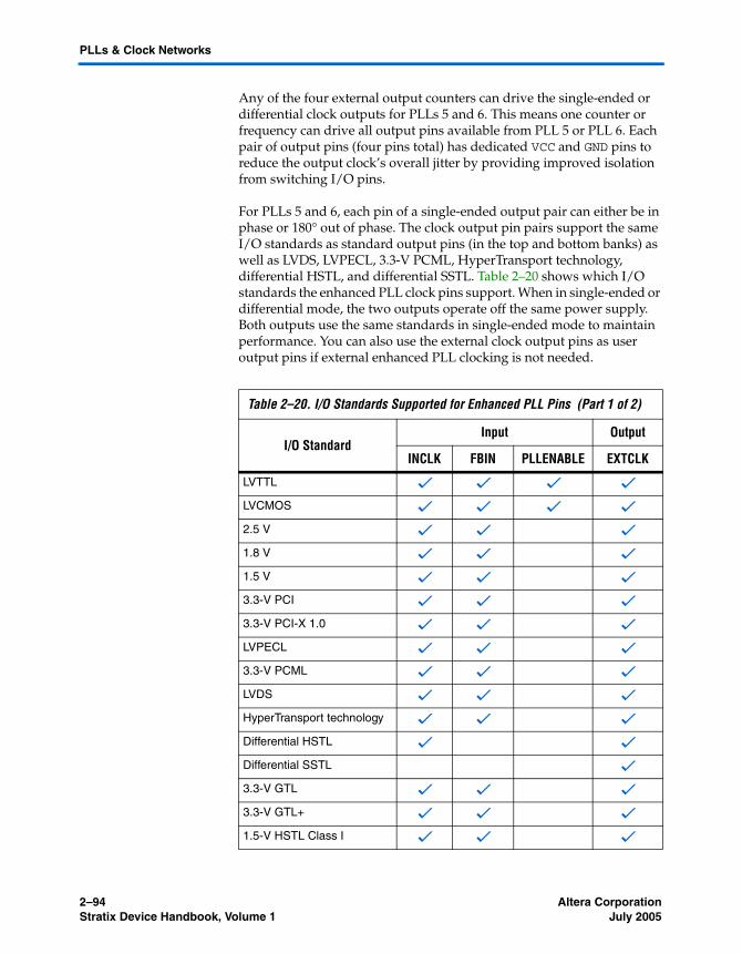
2–94 Altera CorporationStratix Device Handbook, Volume 1 July 2005
PLLs & Clock Networks
Any of the four external output counters can drive the single-ended or differential clock outputs for PLLs 5 and 6. This means one counter or frequency can drive all output pins available from PLL 5 or PLL 6. Each pair of output pins (four pins total) has dedicated VCC and GND pins to reduce the output clock’s overall jitter by providing improved isolation from switching I/O pins.
For PLLs 5 and 6, each pin of a single-ended output pair can either be in phase or 180° out of phase. The clock output pin pairs support the same I/O standards as standard output pins (in the top and bottom banks) as well as LVDS, LVPECL, 3.3-V PCML, HyperTransport technology, differential HSTL, and differential SSTL. Table 2–20 shows which I/O standards the enhanced PLL clock pins support. When in single-ended or differential mode, the two outputs operate off the same power supply. Both outputs use the same standards in single-ended mode to maintain performance. You can also use the external clock output pins as user output pins if external enhanced PLL clocking is not needed.
Table 2–20. I/O Standards Supported for Enhanced PLL Pins (Part 1 of 2)
I/O StandardInput Output
INCLK FBIN PLLENABLE EXTCLK
LVTTL v v v v
LVCMOS v v v v
2.5 V v v v
1.8 V v v v
1.5 V v v v
3.3-V PCI v v v
3.3-V PCI-X 1.0 v v v
LVPECL v v v
3.3-V PCML v v v
LVDS v v v
HyperTransport technology v v v
Differential HSTL v v
Differential SSTL v
3.3-V GTL v v v
3.3-V GTL+ v v v
1.5-V HSTL Class I v v v
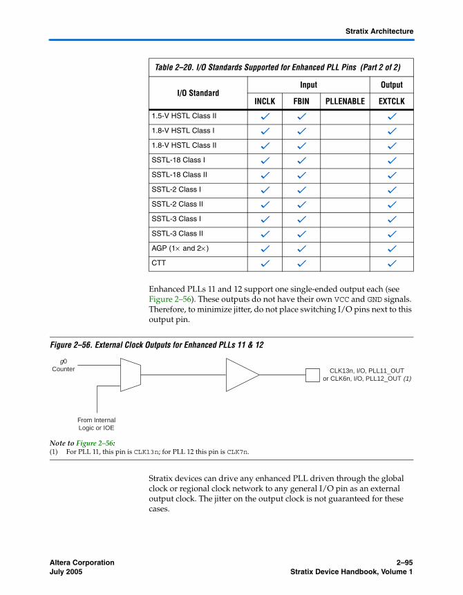
Altera Corporation 2–95July 2005 Stratix Device Handbook, Volume 1
Stratix Architecture
Enhanced PLLs 11 and 12 support one single-ended output each (see Figure 2–56). These outputs do not have their own VCC and GND signals. Therefore, to minimize jitter, do not place switching I/O pins next to this output pin.
Figure 2–56. External Clock Outputs for Enhanced PLLs 11 & 12
Note to Figure 2–56:(1) For PLL 11, this pin is CLK13n; for PLL 12 this pin is CLK7n.
Stratix devices can drive any enhanced PLL driven through the global clock or regional clock network to any general I/O pin as an external output clock. The jitter on the output clock is not guaranteed for these cases.
1.5-V HSTL Class II v v v
1.8-V HSTL Class I v v v
1.8-V HSTL Class II v v v
SSTL-18 Class I v v v
SSTL-18 Class II v v v
SSTL-2 Class I v v v
SSTL-2 Class II v v v
SSTL-3 Class I v v v
SSTL-3 Class II v v v
AGP (1× and 2× ) v v v
CTT v v v
Table 2–20. I/O Standards Supported for Enhanced PLL Pins (Part 2 of 2)
I/O StandardInput Output
INCLK FBIN PLLENABLE EXTCLK
CLK13n, I/O, PLL11_OUTor CLK6n, I/O, PLL12_OUT (1)
From InternalLogic or IOE
g0Counter

2–96 Altera CorporationStratix Device Handbook, Volume 1 July 2005
PLLs & Clock Networks
Clock Feedback
The following four feedback modes in Stratix device enhanced PLLs allow multiplication and/or phase and delay shifting:
■ Zero delay buffer: The external clock output pin is phase-aligned with the clock input pin for zero delay. Altera recommends using the same I/O standard on the input clock and the output clocks for optimum performance.
■ External feedback: The external feedback input pin, FBIN, is phase-aligned with the clock input, CLK, pin. Aligning these clocks allows you to remove clock delay and skew between devices. This mode is only possible for PLLs 5 and 6. PLLs 5 and 6 each support feedback for one of the dedicated external outputs, either one single-ended or one differential pair. In this mode, one e counter feeds back to the PLL FBIN input, becoming part of the feedback loop. Altera recommends using the same I/O standard on the input clock, the FBIN pin, and the output clocks for optimum performance.
■ Normal mode: If an internal clock is used in this mode, it is phase-aligned to the input clock pin. The external clock output pin will have a phase delay relative to the clock input pin if connected in this mode. You define which internal clock output from the PLL should be phase-aligned to the internal clock pin.
■ No compensation: In this mode, the PLL will not compensate for any clock networks or external clock outputs.
Phase & Delay Shifting
Stratix device enhanced PLLs provide advanced programmable phase and clock delay shifting. These parameters are set in the Quartus II software.
Phase DelayThe Quartus II software automatically sets the phase taps and counter settings according to the phase shift entry. You enter a desired phase shift and the Quartus II software automatically sets the closest setting achievable. This type of phase shift is not reconfigurable during system operation. For phase shifting, enter a phase shift (in degrees or time units) for each PLL clock output port or for all outputs together in one shift. You can select phase-shifting values in time units with a resolution of 156.25 to 416.66 ps. This resolution is a function of frequency input and the multiplication and division factors (that is, it is a function of the VCO period), with the finest step being equal to an eighth (×0.125) of the VCO period. Each clock output counter can choose a different phase of the

Altera Corporation 2–97July 2005 Stratix Device Handbook, Volume 1
Stratix Architecture
VCO period from up to eight taps for individual fine step selection. Also, each clock output counter can use a unique initial count setting to achieve individual coarse shift selection in steps of one VCO period. The combination of coarse and fine shifts allows phase shifting for the entire input clock period.
The equation to determine the precision of the phase shifting in degrees is: 45° ÷ post-scale counter value. Therefore, the maximum step size is 45° , and smaller steps are possible depending on the multiplication and division ratio necessary on the output counter port.
This type of phase shift provides the highest precision since it is the least sensitive to process, supply, and temperature variation.
Clock DelayIn addition to the phase shift feature, the ability to fine tune the Δt clock delay provides advanced time delay shift control on each of the four PLL outputs. There are time delays for each post-scale counter (e, g, or l) from the PLL, the n counter, and m counter. Each of these can shift in 250-ps increments for a range of 3.0 ns. The m delay shifts all outputs earlier in time, while n delay shifts all outputs later in time. Individual delays on post-scale counters (e, g, and l) provide positive delay for each output. Table 2–21 shows the combined delay for each output for normal or zero delay buffer mode where Δte, Δtg, or Δtl is unique for each PLL output.
The tOUTPUT for a single output can range from –3 ns to +6 ns. The total delay shift difference between any two PLL outputs, however, must be less than ±3 ns. For example, shifts on two outputs of –1 and +2 ns is allowed, but not –1 and +2.5 ns because these shifts would result in a difference of 3.5 ns. If the design uses external feedback, the Δte delay will remove delay from outputs, represented by a negative sign (see Table 2–21). This effect occurs because the Δte delay is then part of the feedback loop.
Table 2–21. Output Clock Delay for Enhanced PLLs
Normal or Zero Delay Buffer Mode External Feedback Mode
ΔteOUTPUT = Δtn − Δtm + ΔteΔtgOUTPUT = Δtn − Δtm + ΔtgΔtlOUTPUT = Δtn − Δtm + Δtl
ΔteOUTPUT = Δtn − Δtm − Δte (1)ΔtgOUTPUT = Δtn − Δtm + ΔtgΔtlOUTPUT = Δtn − Δtm + Δtl
Note to Table 2–21:(1) Δte removes delay from outputs in external feedback mode.

2–98 Altera CorporationStratix Device Handbook, Volume 1 July 2005
PLLs & Clock Networks
The variation due to process, voltage, and temperature is about ±15% on the delay settings. PLL reconfiguration can control the clock delay shift elements, but not the VCO phase shift multiplexers, during system operation.
Spread-Spectrum Clocking
Stratix device enhanced PLLs use spread-spectrum technology to reduce electromagnetic interference generation from a system by distributing the energy over a broader frequency range. The enhanced PLL typically provides 0.5% down spread modulation using a triangular profile. The modulation frequency is programmable. Enabling spread-spectrum for a PLL affects all of its outputs.
Lock Detect
The lock output indicates that there is a stable clock output signal in phase with the reference clock. Without any additional circuitry, the lock signal may toggle as the PLL begins tracking the reference clock. You may need to gate the lock signal for use as a system control. The lock signal from the locked port can drive the logic array or an output pin.
Whenever the PLL loses lock (for example, inclk jitter, clock switchover, PLL reconfiguration, power supply noise, and so on), the PLL must be reset with the areset signal to guarantee correct phase relationship between the PLL output clocks. If the phase relationship between the input clock versus output clock, and between different output clocks from the PLL is not important in the design, then the PLL need not be reset.
f See the Stratix FPGA Errata Sheet for more information on implementing the gated lock signal in a design.
Programmable Duty Cycle
The programmable duty cycle allows enhanced PLLs to generate clock outputs with a variable duty cycle. This feature is supported on each enhanced PLL post-scale counter (g0..g3, l0..l3, e0..e3). The duty cycle setting is achieved by a low and high time count setting for the post-scale dividers. The Quartus II software uses the frequency input and the required multiply or divide rate to determine the duty cycle choices.
Advanced Clear & Enable Control
There are several control signals for clearing and enabling PLLs and their outputs. You can use these signals to control PLL resynchronization and gate PLL output clocks for low-power applications.
Altera Corporation 2–99July 2005 Stratix Device Handbook, Volume 1
Stratix Architecture
The pllenable pin is a dedicated pin that enables/disables PLLs. When the pllenable pin is low, the clock output ports are driven by GND and all the PLLs go out of lock. When the pllenable pin goes high again, the PLLs relock and resynchronize to the input clocks. You can choose which PLLs are controlled by the pllenable signal by connecting the pllenable input port of the altpll megafunction to the common pllenable input pin.
The areset signals are reset/resynchronization inputs for each PLL. The areset signal should be asserted every time the PLL loses lock to guarantee correct phase relationship between the PLL output clocks. Users should include the areset signal in designs if any of the following conditions are true:
■ PLL Reconfiguration or Clock switchover enables in the design.■ Phase relationships between output clocks need to be maintained
after a loss of lock condition
The device input pins or logic elements (LEs) can drive these input signals. When driven high, the PLL counters will reset, clearing the PLL output and placing the PLL out of lock. The VCO will set back to its nominal setting (~700 MHz). When driven low again, the PLL will resynchronize to its input as it relocks. If the target VCO frequency is below this nominal frequency, then the output frequency will start at a higher value than desired as the PLL locks. If the system cannot tolerate this, the clkena signal can disable the output clocks until the PLL locks.
The pfdena signals control the phase frequency detector (PFD) output with a programmable gate. If you disable the PFD, the VCO operates at its last set value of control voltage and frequency with some long-term drift to a lower frequency. The system continues running when the PLL goes out of lock or the input clock is disabled. By maintaining the last locked frequency, the system has time to store its current settings before shutting down. You can either use your own control signal or a clkloss status signal to trigger pfdena.
The clkena signals control the enhanced PLL regional and global outputs. Each regional and global output port has its own clkena signal. The clkena signals synchronously disable or enable the clock at the PLL output port by gating the outputs of the g and l counters. The clkena signals are registered on the falling edge of the counter output clock to enable or disable the clock without glitches. Figure 2–57 shows the waveform example for a PLL clock port enable. The PLL can remain locked independent of the clkena signals since the loop-related counters are not affected. This feature is useful for applications that require a low power or sleep mode. Upon re-enabling, the PLL does not need a
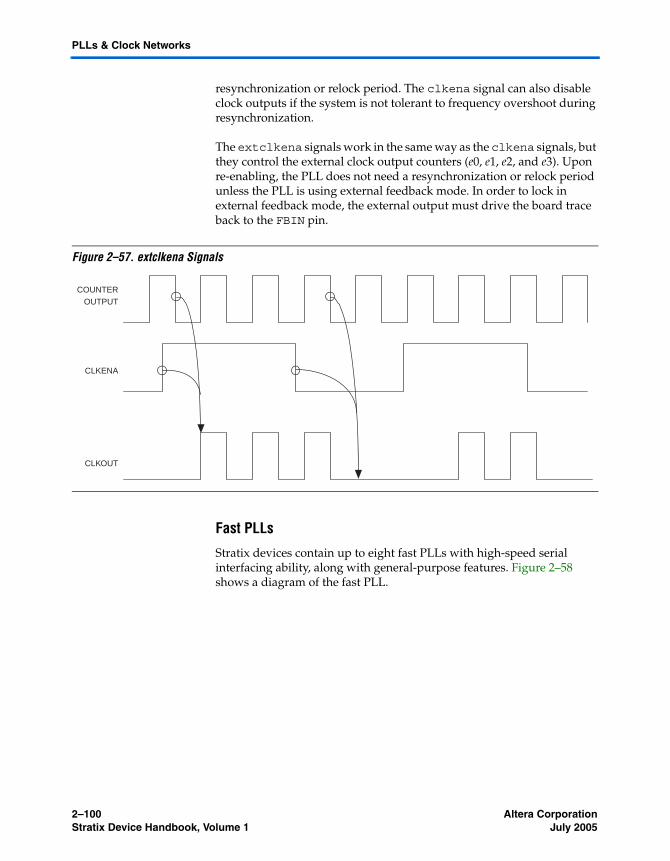
2–100 Altera CorporationStratix Device Handbook, Volume 1 July 2005
PLLs & Clock Networks
resynchronization or relock period. The clkena signal can also disable clock outputs if the system is not tolerant to frequency overshoot during resynchronization.
The extclkena signals work in the same way as the clkena signals, but they control the external clock output counters (e0, e1, e2, and e3). Upon re-enabling, the PLL does not need a resynchronization or relock period unless the PLL is using external feedback mode. In order to lock in external feedback mode, the external output must drive the board trace back to the FBIN pin.
Figure 2–57. extclkena Signals
Fast PLLs
Stratix devices contain up to eight fast PLLs with high-speed serial interfacing ability, along with general-purpose features. Figure 2–58 shows a diagram of the fast PLL.
COUNTEROUTPUT
CLKENA
CLKOUT

Altera Corporation 2–101July 2005 Stratix Device Handbook, Volume 1
Stratix Architecture
Figure 2–58. Stratix Device Fast PLL
Notes to Figure 2–58:(1) The global or regional clock input can be driven by an output from another PLL or any dedicated CLK or FCLK pin.
It cannot be driven by internally-generated global signals.(2) In high-speed differential I/O support mode, this high-speed PLL clock feeds the SERDES. Stratix devices only
support one rate of data transfer per fast PLL in high-speed differential I/O support mode.(3) This signal is a high-speed differential I/O support SERDES control signal.
Clock Multiplication & Division
Stratix device fast PLLs provide clock synthesis for PLL output ports using m/(post scaler) scaling factors. The input clock is multiplied by the m feedback factor. Each output port has a unique post scale counter to divide down the high-frequency VCO. There is one multiply divider, m, per fast PLL with a range of 1 to 32. There are two post scale L dividers for regional and/or LVDS interface clocks, and g0 counter for global clock output port; all range from 1 to 32.
In the case of a high-speed differential interface, set the output counter to 1 to allow the high-speed VCO frequency to drive the SERDES. When used for clocking the SERDES, the m counter can range from 1 to 30. The VCO frequency is equal to fIN×m, where VCO frequency must be between 300 and 1000 MHz.
ChargePump VCO ÷g0
8ClockInput
PFD
÷ l1
÷ l0
÷m
LoopFilter
PhaseFrequencyDetector
VCO Phase SelectionSelectable at each PLLOutput Port
Post-ScaleCounters
Global orregional clock
Global orregional clock
Global orregional clock
diffioclk2 (2)
diffioclk1 (2)
txload_en (3)
rxload_en (3)
Global orregional clock (1)
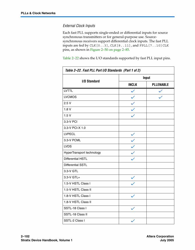
2–102 Altera CorporationStratix Device Handbook, Volume 1 July 2005
PLLs & Clock Networks
External Clock Inputs
Each fast PLL supports single-ended or differential inputs for source synchronous transmitters or for general-purpose use. Source-synchronous receivers support differential clock inputs. The fast PLL inputs are fed by CLK[0..3], CLK[8..11], and FPLL[7..10]CLK pins, as shown in Figure 2–50 on page 2–85.
Table 2–22 shows the I/O standards supported by fast PLL input pins.
Table 2–22. Fast PLL Port I/O Standards (Part 1 of 2)
I/O StandardInput
INCLK PLLENABLE
LVTTL v v
LVCMOS v v
2.5 V v
1.8 V v
1.5 V v
3.3-V PCI
3.3-V PCI-X 1.0
LVPECL v
3.3-V PCML v
LVDS v
HyperTransport technology v
Differential HSTL v
Differential SSTL
3.3-V GTL
3.3-V GTL+ v
1.5-V HSTL Class I v
1.5-V HSTL Class II
1.8-V HSTL Class I v
1.8-V HSTL Class II
SSTL-18 Class I v
SSTL-18 Class II
SSTL-2 Class I v

Altera Corporation 2–103July 2005 Stratix Device Handbook, Volume 1
Stratix Architecture
Table 2–23 shows the performance on each of the fast PLL clock inputs when using LVDS, LVPECL, 3.3-V PCML, or HyperTransport technology.
External Clock Outputs
Each fast PLL supports differential or single-ended outputs for source-synchronous transmitters or for general-purpose external clocks. There are no dedicated external clock output pins. Any I/O pin can be driven by the fast PLL global or regional outputs as an external output pin. The I/O standards supported by any particular bank determines what standards are possible for an external clock output driven by the fast PLL in that bank.
Phase Shifting
Stratix device fast PLLs have advanced clock shift capability that enables programmable phase shifts. You can enter a phase shift (in degrees or time units) for each PLL clock output port or for all outputs together in one shift. You can perform phase shifting in time units with a resolution range of 125 to 416.66 ps. This resolution is a function of the VCO period, with the finest step being equal to an eighth (×0.125) of the VCO period.
SSTL-2 Class II v
SSTL-3 Class I v
SSTL-3 Class II v
AGP (1× and 2× )
CTT v
Table 2–23. LVDS Performance on Fast PLL Input
Fast PLL Clock Input Maximum Input Frequency (MHz)
CLK0, CLK2, CLK9, CLK11, FPLL7CLK, FPLL8CLK, FPLL9CLK, FPLL10CLK
717(1)
CLK1, CLK3, CLK8, CLK10 645
Note to Table 2–23:(1) See the chapter DC & Switching Characteristics of the Stratix Device Handbook,
Volume 1 for more information.
Table 2–22. Fast PLL Port I/O Standards (Part 2 of 2)
I/O StandardInput
INCLK PLLENABLE

2–104 Altera CorporationStratix Device Handbook, Volume 1 July 2005
I/O Structure
Control Signals
The fast PLL has the same lock output, pllenable input, and areset input control signals as the enhanced PLL.
If the input clock stops and causes the PLL to lose lock, then the PLL must be reset for correct phase shift operation.
For more information on high-speed differential I/O support, see “High-Speed Differential I/O Support” on page 2–130.
I/O Structure IOEs provide many features, including:
■ Dedicated differential and single-ended I/O buffers■ 3.3-V, 64-bit, 66-MHz PCI compliance■ 3.3-V, 64-bit, 133-MHz PCI-X 1.0 compliance■ Joint Test Action Group (JTAG) boundary-scan test (BST) support■ Differential on-chip termination for LVDS I/O standard■ Programmable pull-up during configuration■ Output drive strength control■ Slew-rate control■ Tri-state buffers■ Bus-hold circuitry■ Programmable pull-up resistors■ Programmable input and output delays■ Open-drain outputs■ DQ and DQS I/O pins■ Double-data rate (DDR) Registers
The IOE in Stratix devices contains a bidirectional I/O buffer, six registers, and a latch for a complete embedded bidirectional single data rate or DDR transfer. Figure 2–59 shows the Stratix IOE structure. The IOE contains two input registers (plus a latch), two output registers, and two output enable registers. The design can use both input registers and the latch to capture DDR input and both output registers to drive DDR outputs. Additionally, the design can use the output enable (OE) register for fast clock-to-output enable timing. The negative edge-clocked OE register is used for DDR SDRAM interfacing. The Quartus II software automatically duplicates a single OE register that controls multiple output or bidirectional pins.

Altera Corporation 2–105July 2005 Stratix Device Handbook, Volume 1
Stratix Architecture
Figure 2–59. Stratix IOE Structure
The IOEs are located in I/O blocks around the periphery of the Stratix device. There are up to four IOEs per row I/O block and six IOEs per column I/O block. The row I/O blocks drive row, column, or direct link interconnects. The column I/O blocks drive column interconnects. Figure 2–60 shows how a row I/O block connects to the logic array. Figure 2–61 shows how a column I/O block connects to the logic array.
D Q
Output Register
Output A
D Q
Output Register
Output B
Input A
Input B
D Q
OE Register
OE
D Q
OE Register
D Q
Input Register
D Q
Input Register
D Q
Input Latch
Logic Array
CLK
ENA
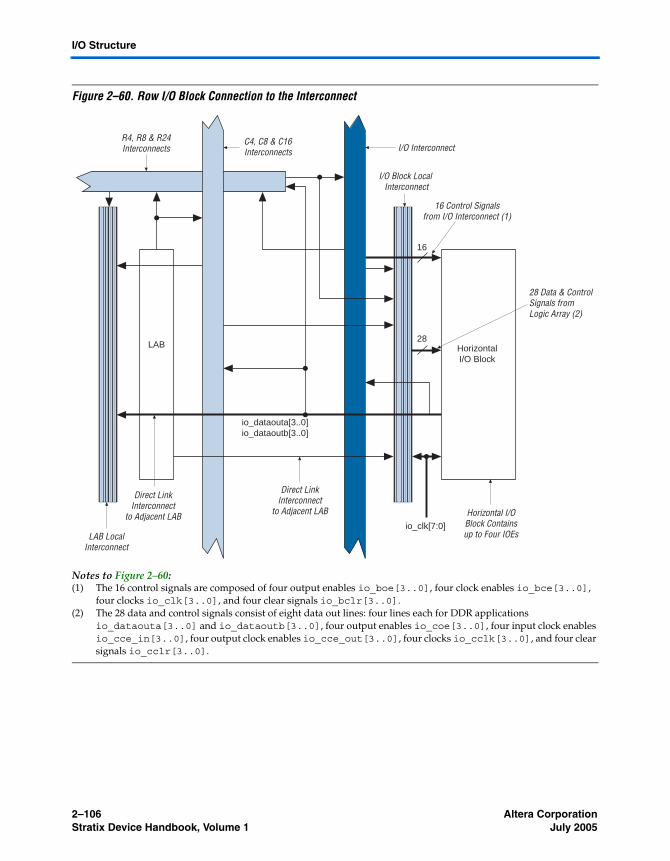
2–106 Altera CorporationStratix Device Handbook, Volume 1 July 2005
I/O Structure
Figure 2–60. Row I/O Block Connection to the Interconnect
Notes to Figure 2–60:(1) The 16 control signals are composed of four output enables io_boe[3..0], four clock enables io_bce[3..0],
four clocks io_clk[3..0], and four clear signals io_bclr[3..0].(2) The 28 data and control signals consist of eight data out lines: four lines each for DDR applications
io_dataouta[3..0] and io_dataoutb[3..0], four output enables io_coe[3..0], four input clock enables io_cce_in[3..0], four output clock enables io_cce_out[3..0], four clocks io_cclk[3..0], and four clear signals io_cclr[3..0].
16
28
R4, R8 & R24Interconnects
C4, C8 & C16Interconnects
I/O Block Local Interconnect
16 Control Signalsfrom I/O Interconnect (1)
I/O Interconnect
28 Data & Control Signals from Logic Array (2)
io_dataouta[3..0]io_dataoutb[3..0]
io_clk[7:0]
Horizontal I/OBlock Containsup to Four IOEs
Direct LinkInterconnect
to Adjacent LAB
Direct LinkInterconnect
to Adjacent LAB
LAB LocalInterconnect
LAB HorizontalI/O Block
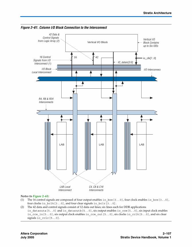
Altera Corporation 2–107July 2005 Stratix Device Handbook, Volume 1
Stratix Architecture
Figure 2–61. Column I/O Block Connection to the Interconnect
Notes to Figure 2–61:(1) The 16 control signals are composed of four output enables io_boe[3..0], four clock enables io_bce[3..0],
four clocks io_bclk[3..0], and four clear signals io_bclr[3..0].(2) The 42 data and control signals consist of 12 data out lines; six lines each for DDR applications
io_dataouta[5..0] and io_dataoutb[5..0], six output enables io_coe[5..0], six input clock enables io_cce_in[5..0], six output clock enables io_cce_out[5..0], six clocks io_cclk[5..0], and six clear signals io_cclr[5..0].
16 Control Signals from I/O Interconnect (1)
42 Data &Control Signals
from Logic Array (2) Vertical I/O Block Containsup to Six IOEs
I/O BlockLocal Interconnect
I/O Interconnect
IO_datain[3:0]
R4, R8 & R24Interconnects
LAB LocalInterconnect
C4, C8 & C16Interconnects
16 42
LAB LAB LAB
io_clk[7..0]
Vertical I/O Block

2–108 Altera CorporationStratix Device Handbook, Volume 1 July 2005
I/O Structure
Stratix devices have an I/O interconnect similar to the R4 and C4 interconnect to drive high-fanout signals to and from the I/O blocks. There are 16 signals that drive into the I/O blocks composed of four output enables io_boe[3..0], four clock enables io_bce[3..0], four clocks io_bclk[3..0], and four clear signals io_bclr[3..0]. The pin’s datain signals can drive the IO interconnect, which in turn drives the logic array or other I/O blocks. In addition, the control and data signals can be driven from the logic array, providing a slower but more flexible routing resource. The row or column IOE clocks, io_clk[7..0], provide a dedicated routing resource for low-skew, high-speed clocks. I/O clocks are generated from regional, global, or fast regional clocks (see “PLLs & Clock Networks” on page 2–73). Figure 2–62 illustrates the signal paths through the I/O block.
Figure 2–62. Signal Path through the I/O Block
Row or Columnio_clk[7..0]
io_boe[3..0]
io_bce[3..0]
io_bclk[3..0]
io_bclr[3..0]
io_datain0
io_datain1
io_dataout0
io_dataout1
io_coe
oe
ce_in
ce_out
io_cce_inaclr/apreset
io_cce_outsclr/spreset
io_cclrclk_in
io_cclkclk_out
ControlSignal
Selection
IOE
From I/OInterconnect
To LogicArray
From LogicArray
To OtherIOEs

Altera Corporation 2–109July 2005 Stratix Device Handbook, Volume 1
Stratix Architecture
Each IOE contains its own control signal selection for the following control signals: oe, ce_in, ce_out, aclr/preset, sclr/preset, clk_in, and clk_out. Figure 2–63 illustrates the control signal selection.
Figure 2–63. Control Signal Selection per IOE
In normal bidirectional operation, the input register can be used for input data requiring fast setup times. The input register can have its own clock input and clock enable separate from the OE and output registers. The output register can be used for data requiring fast clock-to-output performance. The OE register can be used for fast clock-to-output enable timing. The OE and output register share the same clock source and the same clock enable source from local interconnect in the associated LAB, dedicated I/O clocks, and the column and row interconnects. Figure 2–64 shows the IOE in bidirectional configuration.
clk_out
ce_inclk_in
ce_out
aclr/preset
sclr/preset
I/O Interconnect[15..0]
Dedicated I/OClock [7..0]
LocalInterconnect
LocalInterconnect
LocalInterconnect
LocalInterconnect
LocalInterconnect
oe
io_coe
io_cclr
io_cce_out
io_cce_in
io_cclk
io_bclk[3..0] io_bce[3..0] io_bclr[3..0] io_boe[3..0]

2–110 Altera CorporationStratix Device Handbook, Volume 1 July 2005
I/O Structure
Figure 2–64. Stratix IOE in Bidirectional I/O Configuration Note (1)
Note to Figure 2–64:(1) All input signals to the IOE can be inverted at the IOE.
The Stratix device IOE includes programmable delays that can be activated to ensure zero hold times, input IOE register-to-logic array register transfers, or logic array-to-output IOE register transfers.
A path in which a pin directly drives a register may require the delay to ensure zero hold time, whereas a path in which a pin drives a register through combinatorial logic may not require the delay. Programmable delays exist for decreasing input-pin-to-logic-array and IOE input register delays. The Quartus II Compiler can program these delays to automatically minimize setup time while providing a zero hold time. Programmable delays can increase the register-to-pin delays for output
CLRN/PRN
D Q
ENA
Chip-Wide Reset
OE Register
CLRN/PRN
D Q
ENA
Output Register
VCCIO
VCCIO OptionalPCI Clamp
ProgrammablePull-UpResistor
Column or RowInterconnect
I/O Interconnect[15..0]
ioe_clk[7..0]
Bus-HoldCircuit
Output Enable ClockEnable Delay
Output ClockEnable Delay
Logic Array to Output
Register Delay
OutputtZX Delay
OE RegistertCO Delay
CLRN/PRN
D Q
ENA
Input Register
Input ClockEnable Delay
Input Pin toInput Register Delay
Input Pin toLogic Array Delay
Drive Strength Control
Open-Drain Output
Slew Control
sclr/preset
OE
clkout
ce_out
aclr/prn
clkin
ce_in
OutputPin Delay

Altera Corporation 2–111July 2005 Stratix Device Handbook, Volume 1
Stratix Architecture
and/or output enable registers. A programmable delay exists to increase the tZX delay to the output pin, which is required for ZBT interfaces. Table 2–24 shows the programmable delays for Stratix devices.
The IOE registers in Stratix devices share the same source for clear or preset. You can program preset or clear for each individual IOE. You can also program the registers to power up high or low after configuration is complete. If programmed to power up low, an asynchronous clear can control the registers. If programmed to power up high, an asynchronous preset can control the registers. This feature prevents the inadvertent activation of another device’s active-low input upon power-up. If one register in an IOE uses a preset or clear signal then all registers in the IOE must use that same signal if they require preset or clear. Additionally a synchronous reset signal is available for the IOE registers.
Double-Data Rate I/O Pins
Stratix devices have six registers in the IOE, which support DDR interfacing by clocking data on both positive and negative clock edges. The IOEs in Stratix devices support DDR inputs, DDR outputs, and bidirectional DDR modes.
When using the IOE for DDR inputs, the two input registers clock double rate input data on alternating edges. An input latch is also used within the IOE for DDR input acquisition. The latch holds the data that is present during the clock high times. This allows both bits of data to be synchronous with the same clock edge (either rising or falling). Figure 2–65 shows an IOE configured for DDR input. Figure 2–66 shows the DDR input timing diagram.
Table 2–24. Stratix Programmable Delay Chain
Programmable Delays Quartus II Logic Option
Input pin to logic array delay Decrease input delay to internal cells
Input pin to input register delay Decrease input delay to input register
Output pin delay Increase delay to output pin
Output enable register tCO delay Increase delay to output enable pin
Output tZX delay Increase tZX delay to output pin
Output clock enable delay Increase output clock enable delay
Input clock enable delay Increase input clock enable delay
Logic array to output register delay Decrease input delay to output register
Output enable clock enable delay Increase output enable clock enable delay

2–112 Altera CorporationStratix Device Handbook, Volume 1 July 2005
I/O Structure
Figure 2–65. Stratix IOE in DDR Input I/O Configuration Note (1)
Notes to Figure 2–65:(1) All input signals to the IOE can be inverted at the IOE.(2) This signal connection is only allowed on dedicated DQ function pins.(3) This signal is for dedicated DQS function pins only.
CLRN/PRN
D Q
ENA
Chip-Wide Reset
Input Register
CLRN/PRN
D Q
ENA
Input Register
VCCIO
VCCIO
OptionalPCI Clamp
ProgrammablePull-UpResistor
Column or RowInterconnect
I/O Interconnect[15..0]
DQS LocalBus (1), (2)
To DQS LocalBus (3)
ioe_clk[7..0]
Bus-HoldCircuit
Output ClockEnable Delay
CLRN/PRN
D Q
ENA
Latch
Input Pin toInput Register Delay
sclr
clkin
aclr/prn
(1)
(1)
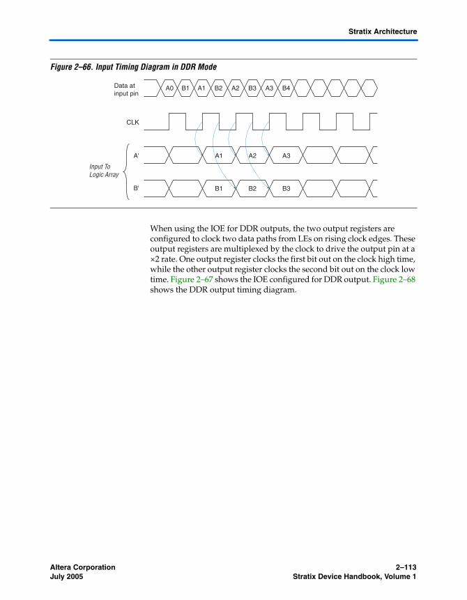
Altera Corporation 2–113July 2005 Stratix Device Handbook, Volume 1
Stratix Architecture
Figure 2–66. Input Timing Diagram in DDR Mode
When using the IOE for DDR outputs, the two output registers are configured to clock two data paths from LEs on rising clock edges. These output registers are multiplexed by the clock to drive the output pin at a ×2 rate. One output register clocks the first bit out on the clock high time, while the other output register clocks the second bit out on the clock low time. Figure 2–67 shows the IOE configured for DDR output. Figure 2–68 shows the DDR output timing diagram.
Data atinput pin
A'
B'
CLK
A0 B1 A1
A1
B2 A2 A3
A2 A3
B1 B2 B3
B3 B4
Input ToLogic Array

2–114 Altera CorporationStratix Device Handbook, Volume 1 July 2005
I/O Structure
Figure 2–67. Stratix IOE in DDR Output I/O Configuration Notes (1), (2)
Notes to Figure 2–67:(1) All input signals to the IOE can be inverted at the IOE.(2) The tristate is by default active high. It can, however, be designed to be active low.
CLRN/PRN
D Q
ENA
Chip-Wide Reset
OE Register
CLRN/PRN
D Q
ENA
OE Register
CLRN/PRN
D Q
ENA
Output Register
VCCIO
VCCIO
OptionalPCI Clamp
ProgrammablePull-UpResistor
Column or RowInterconnect
I/O Interconnect[15..0]
IOE_CLK[7..0]
Bus-HoldCircuit
Logic Arrayto Output
Register Delay
OutputtZX Delay
OE RegistertCO Delay
CLRN/PRN
D Q
ENA
Output RegisterLogic Arrayto Output
Register Delay
Drive Strength Control
Open-Drain Output
Slew Control
Used forDDR SDRAM
clk
sclr
aclr/prn
clkout
OutputPin Delay
Output Enable ClockEnable Delay
Output ClockEnable Delay

Altera Corporation 2–115July 2005 Stratix Device Handbook, Volume 1
Stratix Architecture
Figure 2–68. Output Timing Diagram in DDR Mode
The Stratix IOE operates in bidirectional DDR mode by combining the DDR input and DDR output configurations. Stratix device I/O pins transfer data on a DDR bidirectional bus to support DDR SDRAM. The negative-edge-clocked OE register holds the OE signal inactive until the falling edge of the clock. This is done to meet DDR SDRAM timing requirements.
External RAM Interfacing
Stratix devices support DDR SDRAM at up to 200 MHz (400-Mbps data rate) through dedicated phase-shift circuitry, QDR and QDRII SRAM interfaces up to 167 MHz, and ZBT SRAM interfaces up to 200 MHz. Stratix devices also provide preliminary support for reduced latency DRAM II (RLDRAM II) at rates up to 200 MHz through the dedicated phase-shift circuitry.
1 In addition to the required signals for external memory interfacing, Stratix devices offer the optional clock enable signal. By default the Quartus II software sets the clock enable signal high, which tells the output register to update with new values. The output registers hold their own values if the design sets the clock enable signal low. See Figure 2–64.
f To find out more about the DDR SDRAM specification, see the JEDEC web site (www.jedec.org). For information on memory controller megafunctions for Stratix devices, see the Altera web site (www.altera.com). See AN 342: Interfacing DDR SDRAM with Stratix & Stratix GX Devices for more information on DDR SDRAM interface in Stratix. Also see AN 349: QDR SRAM Controller Reference Design for Stratix & Stratix GX Devices and AN 329: ZBT SRAM Controller Reference Design for Stratix & Stratix GX Devices.
From InternalRegisters
DDR output
CLK
A
B
B1 A1 B2 A2 B3 A3
A2A1 A3 A4
B1 B2 B3 B4

2–116 Altera CorporationStratix Device Handbook, Volume 1 July 2005
I/O Structure
Tables 2–25 and 2–26 show the performance specification for DDR SDRAM, RLDRAM II, QDR SRAM, QDRII SRAM, and ZBT SRAM interfaces in EP1S10 through EP1S40 devices and in EP1S60 and EP1S80 devices. The DDR SDRAM and QDR SRAM numbers in Table 2–25 have been verified with hardware characterization with third-party DDR SDRAM and QDR SRAM devices over temperature and voltage extremes.
Table 2–25. External RAM Support in EP1S10 through EP1S40 Devices
DDR Memory Type I/O Standard
Maximum Clock Rate (MHz)
-5 Speed Grade -6 Speed Grade -7 Speed Grade -8 Speed Grade
Flip-Chip Flip-Chip Wire-Bond
Flip-Chip
Wire-Bond
Flip-Chip
Wire-Bond
DDR SDRAM (1), (2) SSTL-2 200 167 133 133 100 100 100
DDR SDRAM - side banks (2), (3), (4)
SSTL-2 150 133 110 133 100 100 100
RLDRAM II (4) 1.8-V HSTL 200 (5) (5) (5) (5) (5) (5)
QDR SRAM (6) 1.5-V HSTL 167 167 133 133 100 100 100
QDRII SRAM (6) 1.5-V HSTL 200 167 133 133 100 100 100
ZBT SRAM (7) LVTTL 200 200 200 167 167 133 133
Notes to Table 2–25:(1) These maximum clock rates apply if the Stratix device uses DQS phase-shift circuitry to interface with DDR
SDRAM. DQS phase-shift circuitry is only available in the top and bottom I/O banks (I/O banks 3, 4, 7, and 8). (2) For more information on DDR SDRAM, see AN 342: Interfacing DDR SDRAM with Stratix & Stratix GX Devices.(3) DDR SDRAM is supported on the Stratix device side I/O banks (I/O banks 1, 2, 5, and 6) without dedicated DQS
phase-shift circuitry. The read DQS signal is ignored in this mode.(4) These performance specifications are preliminary.(5) This device does not support RLDRAM II.(6) For more information on QDR or QDRII SRAM, see AN 349: QDR SRAM Controller Reference Design for Stratix &
Stratix GX Devices.(7) For more information on ZBT SRAM, see AN 329: ZBT SRAM Controller Reference Design for Stratix & Stratix GX
Devices.

Altera Corporation 2–117July 2005 Stratix Device Handbook, Volume 1
Stratix Architecture
In addition to six I/O registers and one input latch in the IOE for interfacing to these high-speed memory interfaces, Stratix devices also have dedicated circuitry for interfacing with DDR SDRAM. In every Stratix device, the I/O banks at the top (I/O banks 3 and 4) and bottom (I/O banks 7 and 8) of the device support DDR SDRAM up to 200 MHz. These pins support DQS signals with DQ bus modes of ×8, ×16, or ×32.
Table 2–27 shows the number of DQ and DQS buses that are supported per device.
Table 2–26. External RAM Support in EP1S60 & EP1S80 Devices
DDR Memory Type I/O StandardMaximum Clock Rate (MHz)
-5 Speed Grade -6 Speed Grade -7 Speed Grade
DDR SDRAM (1), (2) SSTL-2 167 167 133
DDR SDRAM - side banks (2), (3) SSTL-2 150 133 133
QDR SRAM (4) 1.5-V HSTL 133 133 133
QDRII SRAM (4) 1.5-V HSTL 167 167 133
ZBT SRAM (5) LVTTL 200 200 167
Notes to Table 2–26:(1) These maximum clock rates apply if the Stratix device uses DQS phase-shift circuitry to interface with DDR
SDRAM. DQS phase-shift circuitry is only available in the top and bottom I/O banks (I/O banks 3, 4, 7, and 8). (2) For more information on DDR SDRAM, see AN 342: Interfacing DDR SDRAM with Stratix & Stratix GX Devices.(3) DDR SDRAM is supported on the Stratix device side I/O banks (I/O banks 1, 2, 5, and 6) without dedicated DQS
phase-shift circuitry. The read DQS signal is ignored in this mode. Numbers are preliminary.(4) For more information on QDR or QDRII SRAM, see AN 349: QDR SRAM Controller Reference Design for Stratix &
Stratix GX Devices.(5) For more information on ZBT SRAM, see AN 329: ZBT SRAM Controller Reference Design for Stratix & Stratix GX
Devices.
Table 2–27. DQS & DQ Bus Mode Support (Part 1 of 2) Note (1)
Device Package Number of ×8 Groups
Number of ×16 Groups
Number of ×32 Groups
EP1S10 672-pin BGA672-pin FineLine BGA
12 (2) 0 0
484-pin FineLine BGA780-pin FineLine BGA
16 (3) 0 4
EP1S20 484-pin FineLine BGA 18(4) 7 (5) 4
672-pin BGA672-pin FineLine BGA
16(3) 7 (5) 4
780-pin FineLine BGA 20 7 (5) 4

2–118 Altera CorporationStratix Device Handbook, Volume 1 July 2005
I/O Structure
A compensated delay element on each DQS pin automatically aligns input DQS synchronization signals with the data window of their corresponding DQ data signals. The DQS signals drive a local DQS bus in the top and bottom I/O banks. This DQS bus is an additional resource to the I/O clocks and is used to clock DQ input registers with the DQS signal.
Two separate single phase-shifting reference circuits are located on the top and bottom of the Stratix device. Each circuit is driven by a system reference clock through the CLK pins that is the same frequency as the DQS signal. Clock pins CLK[15..12]p feed the phase-shift circuitry on the top of the device and clock pins CLK[7..4]p feed the phase-shift circuitry on the bottom of the device. The phase-shifting reference circuit on the top of the device controls the compensated delay elements for all 10 DQS pins located at the top of the device. The phase-shifting reference circuit on the bottom of the device controls the compensated delay elements for all 10 DQS pins located on the bottom of the device. All 10 delay elements (DQS signals) on either the top or bottom of the device
EP1S25 672-pin BGA672-pin FineLine BGA
16 (3) 8 4
780-pin FineLine BGA1,020-pin FineLine BGA
20 8 4
EP1S30 956-pin BGA780-pin FineLine BGA1,020-pin FineLine BGA
20 8 4
EP1S40 956-pin BGA1,020-pin FineLine BGA1,508-pin FineLine BGA
20 8 4
EP1S60 956-pin BGA1,020-pin FineLine BGA1,508-pin FineLine BGA
20 8 4
EP1S80 956-pin BGA1,508-pin FineLine BGA1,923-pin FineLine BGA
20 8 4
Notes to Table 2–27:(1) See the Selectable I/O Standards in Stratix & Stratix GX Devices chapter in the Stratix Device Handbook, Volume 2
for VREF guidelines.(2) These packages have six groups in I/O banks 3 and 4 and six groups in I/O banks 7 and 8.(3) These packages have eight groups in I/O banks 3 and 4 and eight groups in I/O banks 7 and 8.(4) This package has nine groups in I/O banks 3 and 4 and nine groups in I/O banks 7 and 8.(5) These packages have three groups in I/O banks 3 and 4 and four groups in I/O banks 7 and 8.
Table 2–27. DQS & DQ Bus Mode Support (Part 2 of 2) Note (1)
Device Package Number of ×8 Groups
Number of ×16 Groups
Number of ×32 Groups
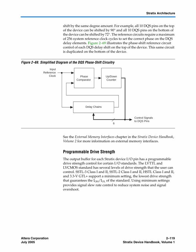
Altera Corporation 2–119July 2005 Stratix Device Handbook, Volume 1
Stratix Architecture
shift by the same degree amount. For example, all 10 DQS pins on the top of the device can be shifted by 90° and all 10 DQS pins on the bottom of the device can be shifted by 72°. The reference circuits require a maximum of 256 system reference clock cycles to set the correct phase on the DQS delay elements. Figure 2–69 illustrates the phase-shift reference circuit control of each DQS delay shift on the top of the device. This same circuit is duplicated on the bottom of the device.
Figure 2–69. Simplified Diagram of the DQS Phase-Shift Circuitry
See the External Memory Interfaces chapter in the Stratix Device Handbook, Volume 2 for more information on external memory interfaces.
Programmable Drive Strength
The output buffer for each Stratix device I/O pin has a programmable drive strength control for certain I/O standards. The LVTTL and LVCMOS standard has several levels of drive strength that the user can control. SSTL-3 Class I and II, SSTL-2 Class I and II, HSTL Class I and II, and 3.3-V GTL+ support a minimum setting, the lowest drive strength that guarantees the IOH/IOL of the standard. Using minimum settings provides signal slew rate control to reduce system noise and signal overshoot.
PhaseComparator
Up/DownCounter
Delay Chains
InputReference
Clock
Control Signalsto DQS Pins
6
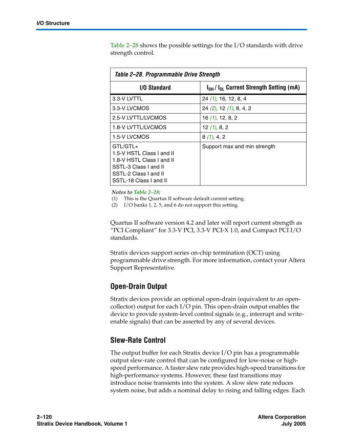
2–120 Altera CorporationStratix Device Handbook, Volume 1 July 2005
I/O Structure
Table 2–28 shows the possible settings for the I/O standards with drive strength control.
Quartus II software version 4.2 and later will report current strength as “PCI Compliant” for 3.3-V PCI, 3.3-V PCI-X 1.0, and Compact PCI I/O standards.
Stratix devices support series on-chip termination (OCT) using programmable drive strength. For more information, contact your Altera Support Representative.
Open-Drain Output
Stratix devices provide an optional open-drain (equivalent to an open-collector) output for each I/O pin. This open-drain output enables the device to provide system-level control signals (e.g., interrupt and write-enable signals) that can be asserted by any of several devices.
Slew-Rate Control
The output buffer for each Stratix device I/O pin has a programmable output slew-rate control that can be configured for low-noise or high-speed performance. A faster slew rate provides high-speed transitions for high-performance systems. However, these fast transitions may introduce noise transients into the system. A slow slew rate reduces system noise, but adds a nominal delay to rising and falling edges. Each
Table 2–28. Programmable Drive Strength
I/O Standard IOH / IOL Current Strength Setting (mA)
3.3-V LVTTL 24 (1), 16, 12, 8, 4
3.3-V LVCMOS 24 (2), 12 (1), 8, 4, 2
2.5-V LVTTL/LVCMOS 16 (1), 12, 8, 2
1.8-V LVTTL/LVCMOS 12 (1), 8, 2
1.5-V LVCMOS 8 (1), 4, 2
GTL/GTL+1.5-V HSTL Class I and II1.8-V HSTL Class I and IISSTL-3 Class I and IISSTL-2 Class I and IISSTL-18 Class I and II
Support max and min strength
Notes to Table 2–28:(1) This is the Quartus II software default current setting.(2) I/O banks 1, 2, 5, and 6 do not support this setting.

Altera Corporation 2–121July 2005 Stratix Device Handbook, Volume 1
Stratix Architecture
I/O pin has an individual slew-rate control, allowing you to specify the slew rate on a pin-by-pin basis. The slew-rate control affects both the rising and falling edges.
Bus Hold
Each Stratix device I/O pin provides an optional bus-hold feature. The bus-hold circuitry can weakly hold the signal on an I/O pin at its last-driven state. Since the bus-hold feature holds the last-driven state of the pin until the next input signal is present, an external pull-up or pull-down resistor is not needed to hold a signal level when the bus is tri-stated.
Table 2–29 shows bus hold support for different pin types.
The bus-hold circuitry also pulls undriven pins away from the input threshold voltage where noise can cause unintended high-frequency switching. You can select this feature individually for each I/O pin. The bus-hold output drives no higher than VCCIO to prevent overdriving signals. If the bus-hold feature is enabled, the programmable pull-up option cannot be used. Disable the bus-hold feature when using open-drain outputs with the GTL+ I/O standard or when the I/O pin has been configured for differential signals.
The bus-hold circuitry uses a resistor with a nominal resistance (RBH) of approximately 7 kΩ to weakly pull the signal level to the last-driven state. See the DC & Switching Characteristics chapter of the Stratix Device Handbook, Volume 1 for the specific sustaining current driven through this resistor and overdrive current used to identify the next-driven input level. This information is provided for each VCCIO voltage level.
The bus-hold circuitry is active only after configuration. When going into user mode, the bus-hold circuit captures the value on the pin present at the end of configuration.
Table 2–29. Bus Hold Support
Pin Type Bus Hold
I/O pins v
CLK[15..0]
CLK[0,1,2,3,8,9,10,11]
FCLK v
FPLL[7..10]CLK
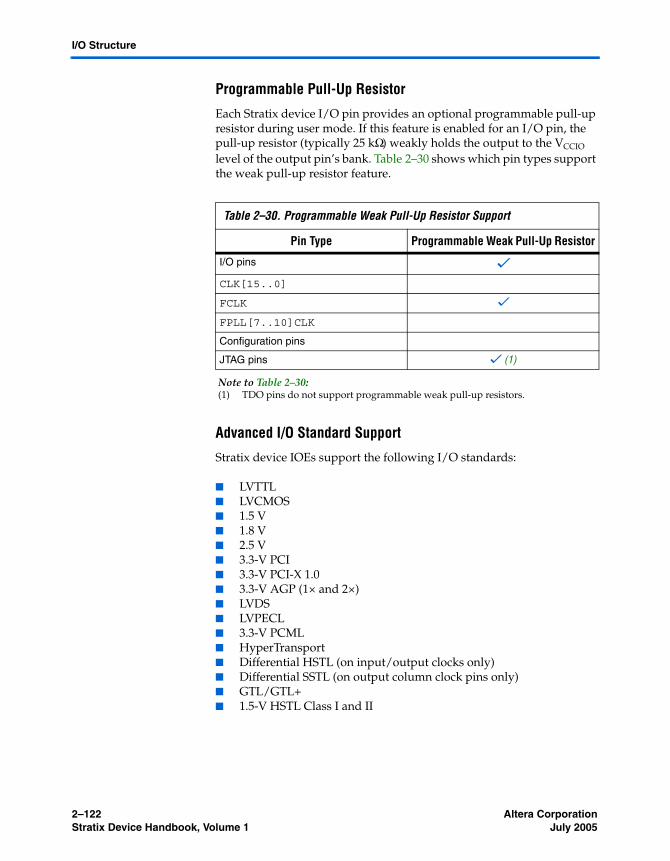
2–122 Altera CorporationStratix Device Handbook, Volume 1 July 2005
I/O Structure
Programmable Pull-Up Resistor
Each Stratix device I/O pin provides an optional programmable pull-up resistor during user mode. If this feature is enabled for an I/O pin, the pull-up resistor (typically 25 kΩ) weakly holds the output to the VCCIO level of the output pin’s bank. Table 2–30 shows which pin types support the weak pull-up resistor feature.
Advanced I/O Standard Support
Stratix device IOEs support the following I/O standards:
■ LVTTL■ LVCMOS■ 1.5 V■ 1.8 V■ 2.5 V■ 3.3-V PCI■ 3.3-V PCI-X 1.0■ 3.3-V AGP (1× and 2×)■ LVDS■ LVPECL■ 3.3-V PCML ■ HyperTransport■ Differential HSTL (on input/output clocks only)■ Differential SSTL (on output column clock pins only)■ GTL/GTL+■ 1.5-V HSTL Class I and II
Table 2–30. Programmable Weak Pull-Up Resistor Support
Pin Type Programmable Weak Pull-Up Resistor
I/O pins v
CLK[15..0]
FCLK v
FPLL[7..10]CLK
Configuration pins
JTAG pins v (1)
Note to Table 2–30:(1) TDO pins do not support programmable weak pull-up resistors.

Altera Corporation 2–123July 2005 Stratix Device Handbook, Volume 1
Stratix Architecture
■ 1.8-V HSTL Class I and II■ SSTL-3 Class I and II■ SSTL-2 Class I and II■ SSTL-18 Class I and II■ CTT
Table 2–31 describes the I/O standards supported by Stratix devices.
Table 2–31. Stratix Supported I/O Standards
I/O Standard TypeInput Reference Voltage (VREF)
(V)
Output Supply Voltage (VCCIO)
(V)
Board Termination Voltage (VTT)
(V)
LVTTL Single-ended N/A 3.3 N/A
LVCMOS Single-ended N/A 3.3 N/A
2.5 V Single-ended N/A 2.5 N/A
1.8 V Single-ended N/A 1.8 N/A
1.5 V Single-ended N/A 1.5 N/A
3.3-V PCI Single-ended N/A 3.3 N/A
3.3-V PCI-X 1.0 Single-ended N/A 3.3 N/A
LVDS Differential N/A 3.3 N/A
LVPECL Differential N/A 3.3 N/A
3.3-V PCML Differential N/A 3.3 N/A
HyperTransport Differential N/A 2.5 N/A
Differential HSTL (1) Differential 0.75 1.5 0.75
Differential SSTL (2) Differential 1.25 2.5 1.25
GTL Voltage-referenced 0.8 N/A 1.20
GTL+ Voltage-referenced 1.0 N/A 1.5
1.5-V HSTL Class I and II Voltage-referenced 0.75 1.5 0.75
1.8-V HSTL Class I and II Voltage-referenced 0.9 1.8 0.9
SSTL-18 Class I and II Voltage-referenced 0.90 1.8 0.90
SSTL-2 Class I and II Voltage-referenced 1.25 2.5 1.25
SSTL-3 Class I and II Voltage-referenced 1.5 3.3 1.5
AGP (1× and 2° ) Voltage-referenced 1.32 3.3 N/A
CTT Voltage-referenced 1.5 3.3 1.5
Notes to Table 2–31:(1) This I/O standard is only available on input and output clock pins.(2) This I/O standard is only available on output column clock pins.
2–124 Altera CorporationStratix Device Handbook, Volume 1 July 2005
I/O Structure
f For more information on I/O standards supported by Stratix devices, see the Selectable I/O Standards in Stratix & Stratix GX Devices chapter of the Stratix Device Handbook, Volume 2.
Stratix devices contain eight I/O banks in addition to the four enhanced PLL external clock out banks, as shown in Figure 2–70. The four I/O banks on the right and left of the device contain circuitry to support high-speed differential I/O for LVDS, LVPECL, 3.3-V PCML, and HyperTransport inputs and outputs. These banks support all I/O standards listed in Table 2–31 except PCI I/O pins or PCI-X 1.0, GTL, SSTL-18 Class II, and HSTL Class II outputs. The top and bottom I/O banks support all single-ended I/O standards. Additionally, Stratix devices support four enhanced PLL external clock output banks, allowing clock output capabilities such as differential support for SSTL and HSTL. Table 2–32 shows I/O standard support for each I/O bank.

Altera Corporation 2–125July 2005 Stratix Device Handbook, Volume 1
Stratix Architecture
Figure 2–70. Stratix I/O Banks Notes (1), (2), (3)
Notes to Figure 2–70:(1) Figure 2–70 is a top view of the silicon die. This will correspond to a top-down view for non-flip-chip packages, but
will be a reverse view for flip-chip packages.(2) Figure 2–70 is a graphic representation only. See the device pin-outs on the web (www.altera.com) and the
Quartus II software for exact locations.(3) Banks 9 through 12 are enhanced PLL external clock output banks.(4) If the high-speed differential I/O pins are not used for high-speed differential signaling, they can support all of the
I/O standards except HSTL Class I and II, GTL, SSTL-18 Class II, PCI, PCI-X 1.0, and AGP 1× /2× .
(5) For guidelines for placing single-ended I/O pads next to differential I/O pads, see the Selectable I/O Standards in Stratix and Stratix GX Devices chapter in the Stratix Device Handbook, Volume 2.
LVDS, LVPECL, 3.3-V PCML, and HyperTransport I/O Blockand Regular I/O Pins (4)
LVDS, LVPECL, 3.3-V PCML, and HyperTransport I/O Block
and Regular I/O Pins (4)
I/O Banks 3, 4, 9 & 10 Support All Single-Ended I/O Standards
I/O Banks 7, 8, 11 & 12 Support All Single-Ended I/O Standards
I/O Banks 1, 2, 5, and 6 Support AllSingle-Ended I/O Standards Except Differential HSTL Output Clocks, Differential SSTL-2 Output Clocks, HSTL Class II, GTL, SSTL-18 Class II, PCI, PCI-X 1.0, and AGP 1×/2×
DQS9T DQS8T DQS7T DQS6T DQS5T DQS4T DQS3T DQS2T DQS1T DQS0TPLL5
VREF1B3 VREF2B3 VREF3B3 VREF4B3 VREF5B3 VREF1B4 VREF2B4 VREF3B4 VREF4B4 VREF5B4
VREF5B8 VREF4B8 VREF3B8 VREF2B8 VREF1B8 VREF5B7 VREF4B7 VREF3B7 VREF2B7 VREF1B7PLL6
DQS9B DQS8B DQS7B DQS6B DQS5B DQS4B DQS3B DQS2B DQS1B DQS0B
9 10
VR
EF
1B2
VR
EF
2B2
VR
EF
3B2
VR
EF
4B2
VR
EF
1B1
VR
EF
2B1
VR
EF
3B1
VR
EF
4B1
VR
EF
4B6
VR
EF
3B6
VR
EF
2B6
VR
EF
1B6
VR
EF
4B5
VR
EF
3B5
VR
EF
2B5
VR
EF
1B5
Ban
k 5
Ban
k 6
PLL3
PLL4PLL1
PLL2
Ban
k 1
Ban
k 2
Bank 3 Bank 4
11 12Bank 8 Bank 7
LVDS, LVPECL, 3.3-V PCML, and HyperTransport I/O Blockand Regular I/O Pins (4)
LVDS, LVPECL, 3.3-V PCML, and HyperTransport I/O Block
and Regular I/O Pins (4)
PLL7 PLL10
PLL8 PLL9PLL12
PLL11
(5)
(5)
(5)
(5)
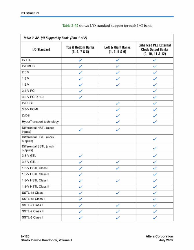
2–126 Altera CorporationStratix Device Handbook, Volume 1 July 2005
I/O Structure
Table 2–32 shows I/O standard support for each I/O bank.
Table 2–32. I/O Support by Bank (Part 1 of 2)
I/O Standard Top & Bottom Banks (3, 4, 7 & 8)
Left & Right Banks (1, 2, 5 & 6)
Enhanced PLL External Clock Output Banks
(9, 10, 11 & 12)
LVTTL v v v
LVCMOS v v v
2.5 V v v v
1.8 V v v v
1.5 V v v v
3.3-V PCI v v
3.3-V PCI-X 1.0 v v
LVPECL v v
3.3-V PCML v v
LVDS v v
HyperTransport technology v v
Differential HSTL (clock inputs) v v
Differential HSTL (clock outputs) v
Differential SSTL (clock outputs) v
3.3-V GTL v v
3.3-V GTL+ v v v
1.5-V HSTL Class I v v v
1.5-V HSTL Class II v v
1.8-V HSTL Class I v v v
1.8-V HSTL Class II v v
SSTL-18 Class I v v v
SSTL-18 Class II v v
SSTL-2 Class I v v v
SSTL-2 Class II v v v
SSTL-3 Class I v v v
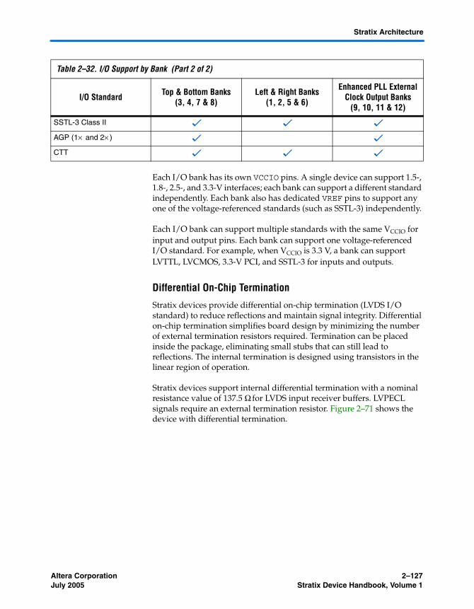
Altera Corporation 2–127July 2005 Stratix Device Handbook, Volume 1
Stratix Architecture
Each I/O bank has its own VCCIO pins. A single device can support 1.5-, 1.8-, 2.5-, and 3.3-V interfaces; each bank can support a different standard independently. Each bank also has dedicated VREF pins to support any one of the voltage-referenced standards (such as SSTL-3) independently.
Each I/O bank can support multiple standards with the same VCCIO for input and output pins. Each bank can support one voltage-referenced I/O standard. For example, when VCCIO is 3.3 V, a bank can support LVTTL, LVCMOS, 3.3-V PCI, and SSTL-3 for inputs and outputs.
Differential On-Chip Termination
Stratix devices provide differential on-chip termination (LVDS I/O standard) to reduce reflections and maintain signal integrity. Differential on-chip termination simplifies board design by minimizing the number of external termination resistors required. Termination can be placed inside the package, eliminating small stubs that can still lead to reflections. The internal termination is designed using transistors in the linear region of operation.
Stratix devices support internal differential termination with a nominal resistance value of 137.5 Ω for LVDS input receiver buffers. LVPECL signals require an external termination resistor. Figure 2–71 shows the device with differential termination.
SSTL-3 Class II v v v
AGP (1× and 2× ) v v
CTT v v v
Table 2–32. I/O Support by Bank (Part 2 of 2)
I/O Standard Top & Bottom Banks (3, 4, 7 & 8)
Left & Right Banks (1, 2, 5 & 6)
Enhanced PLL External Clock Output Banks
(9, 10, 11 & 12)
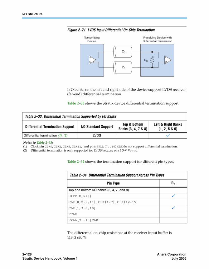
2–128 Altera CorporationStratix Device Handbook, Volume 1 July 2005
I/O Structure
Figure 2–71. LVDS Input Differential On-Chip Termination
I/O banks on the left and right side of the device support LVDS receiver (far-end) differential termination.
Table 2–33 shows the Stratix device differential termination support.
Table 2–34 shows the termination support for different pin types.
The differential on-chip resistance at the receiver input buffer is 118 Ω ±20 %.
RD+
Ð
+
Ð
TransmittingDevice
Receiving Device withDifferential Termination
Z0
Z0
Table 2–33. Differential Termination Supported by I/O Banks
Differential Termination Support I/O Standard Support Top & Bottom Banks (3, 4, 7 & 8)
Left & Right Banks (1, 2, 5 & 6)
Differential termination (1), (2) LVDS v
Notes to Table 2–33:(1) Clock pin CLK0, CLK2, CLK9, CLK11, and pins FPLL[7..10]CLK do not support differential termination.(2) Differential termination is only supported for LVDS because of a 3.3-V VC C I O.
Table 2–34. Differential Termination Support Across Pin Types
Pin Type RD
Top and bottom I/O banks (3, 4, 7, and 8)
DIFFIO_RX[] v
CLK[0,2,9,11],CLK[4-7],CLK[12-15]
CLK[1,3,8,10] v
FCLK
FPLL[7..10]CLK

Altera Corporation 2–129July 2005 Stratix Device Handbook, Volume 1
Stratix Architecture
However, there is additional resistance present between the device ball and the input of the receiver buffer, as shown in Figure 2–72. This resistance is because of package trace resistance (which can be calculated as the resistance from the package ball to the pad) and the parasitic layout metal routing resistance (which is shown between the pad and the intersection of the on-chip termination and input buffer).
Figure 2–72. Differential Resistance of LVDS Differential Pin Pair (RD)
Table 2–35 defines the specification for internal termination resistance for commercial devices.
MultiVolt I/O Interface
The Stratix architecture supports the MultiVolt I/O interface feature, which allows Stratix devices in all packages to interface with systems of different supply voltages.
The Stratix VCCINT pins must always be connected to a 1.5-V power supply. With a 1.5-V VCCINT level, input pins are 1.5-V, 1.8-V, 2.5-V, and 3.3-V tolerant. The VCCIO pins can be connected to either a 1.5-V, 1.8-V, 2.5-V, or 3.3-V power supply, depending on the output requirements.
LVDSInput Buffer
Differential On-ChipTermination Resistor
9.3 Ω
9.3 Ω
0.3 Ω
0.3 Ω
RD
PadPackage Ball
Table 2–35. Differential On-Chip Termination
Symbol Description Conditions Resistance
UnitMin Typ Max
RD (2) Internal differential termination for LVDS Commercial (1), (3) 110 135 165 W
Industrial (2), (3) 100 135 170 W
Notes to Table 2–35:(1) Data measured over minimum conditions (Tj = 0 C, VC C I O +5%) and maximum conditions (Tj = 85 C,
VC C I O = –5%).(2) Data measured over minimum conditions (Tj = –40 C, VCCIO +5%) and maximum conditions (Tj = 100 C,
VCCIO = –5%).(3) LVDS data rate is supported for 840 Mbps using internal differential termination.

2–130 Altera CorporationStratix Device Handbook, Volume 1 July 2005
High-Speed Differential I/O Support
The output levels are compatible with systems of the same voltage as the power supply (i.e., when VCCIO pins are connected to a 1.5-V power supply, the output levels are compatible with 1.5-V systems). When VCCIO pins are connected to a 3.3-V power supply, the output high is 3.3 V and is compatible with 3.3-V or 5.0-V systems.
Table 2–36 summarizes Stratix MultiVolt I/O support.
High-Speed Differential I/O Support
Stratix devices contain dedicated circuitry for supporting differential standards at speeds up to 840 Mbps. The following differential I/O standards are supported in the Stratix device: LVDS, LVPECL, HyperTransport, and 3.3-V PCML.
There are four dedicated high-speed PLLs in the EP1S10 to EP1S25 devices and eight dedicated high-speed PLLs in the EP1S30 to EP1S80 devices to multiply reference clocks and drive high-speed differential SERDES channels.
f See the Stratix device pin-outs at www.altera.com for additional high speed DIFFIO pin information for Stratix devices.
Table 2–36. Stratix MultiVolt I/O Support Note (1)
VCCIO (V)Input Signal (5) Output Signal (6)
1.5 V 1.8 V 2.5 V 3.3 V 5.0 V 1.5 V 1.8 V 2.5 V 3.3 V 5.0 V
1.5 v v v (2) v (2) v
1.8 v (2) v v (2) v (2) v (3) v
2.5 v v v (3) v (3) v
3.3 v (2) v v (4) v (3) v (3) v (3) v v
Notes to Table 2–36:(1) To drive inputs higher than VCCIO but less than 4.1 V, disable the PCI clamping diode. However, to drive 5.0-V
inputs to the device, enable the PCI clamping diode to prevent VI from rising above 4.0 V.(2) The input pin current may be slightly higher than the typical value.(3) Although VCCIO specifies the voltage necessary for the Stratix device to drive out, a receiving device powered at a
different level can still interface with the Stratix device if it has inputs that tolerate the VCCIO value.(4) Stratix devices can be 5.0-V tolerant with the use of an external resistor and the internal PCI clamp diode.(5) This is the external signal that is driving the Stratix device.(6) This represents the system voltage that Stratix supports when a VCCIO pin is connected to a specific voltage level.
For example, when VCCIO is 3.3 V and if the I/O standard is LVTTL/LVCMOS, the output high of the signal coming out from Stratix is 3.3 V and is compatible with 3.3-V or 5.0-V systems.

Altera Corporation 2–131July 2005 Stratix Device Handbook, Volume 1
Stratix Architecture
Table 2–37 shows the number of channels that each fast PLL can clock in EP1S10, EP1S20, and EP1S25 devices. Tables 2–38 through Table 2–41 show this information for EP1S30, EP1S40, EP1S60, and EP1S80 devices.
Table 2–37. EP1S10, EP1S20 & EP1S25 Device Differential Channels (Part 1 of 2) Note (1)
Device Package Transmitter/Receiver
Total Channels
Maximum Speed (Mbps)
Center Fast PLLs
PLL 1 PLL 2 PLL 3 PLL 4
EP1S10 484-pin FineLine BGA Transmitter (2) 20 840 (4) 5 5 5 5
840 (3) 10 10 10 10
Receiver 20 840 (4) 5 5 5 5
840 (3) 10 10 10 10
672-pin FineLine BGA672-pin BGA
Transmitter (2) 36 624 (4) 9 9 9 9
624 (3) 18 18 18 18
Receiver 36 624 (4) 9 9 9 9
624 (3) 18 18 18 18
780-pin FineLine BGA Transmitter (2) 44 840 (4) 11 11 11 11
840 (3) 22 22 22 22
Receiver 44 840 (4) 11 11 11 11
840 (3) 22 22 22 22
EP1S20 484-pin FineLine BGA Transmitter (2) 24 840 (4) 6 6 6 6
840 (3) 12 12 12 12
Receiver 20 840 (4) 5 5 5 5
840 (3) 10 10 10 10
672-pin FineLine BGA672-pin BGA
Transmitter (2) 48 624 (4) 12 12 12 12
624 (3) 24 24 24 24
Receiver 50 624 (4) 13 12 12 13
624 (3) 25 25 25 25
780-pin FineLine BGA Transmitter (2) 66 840 (4) 17 16 16 17
840 (3) 33 33 33 33
Receiver 66 840 (4) 17 16 16 17
840 (3) 33 33 33 33
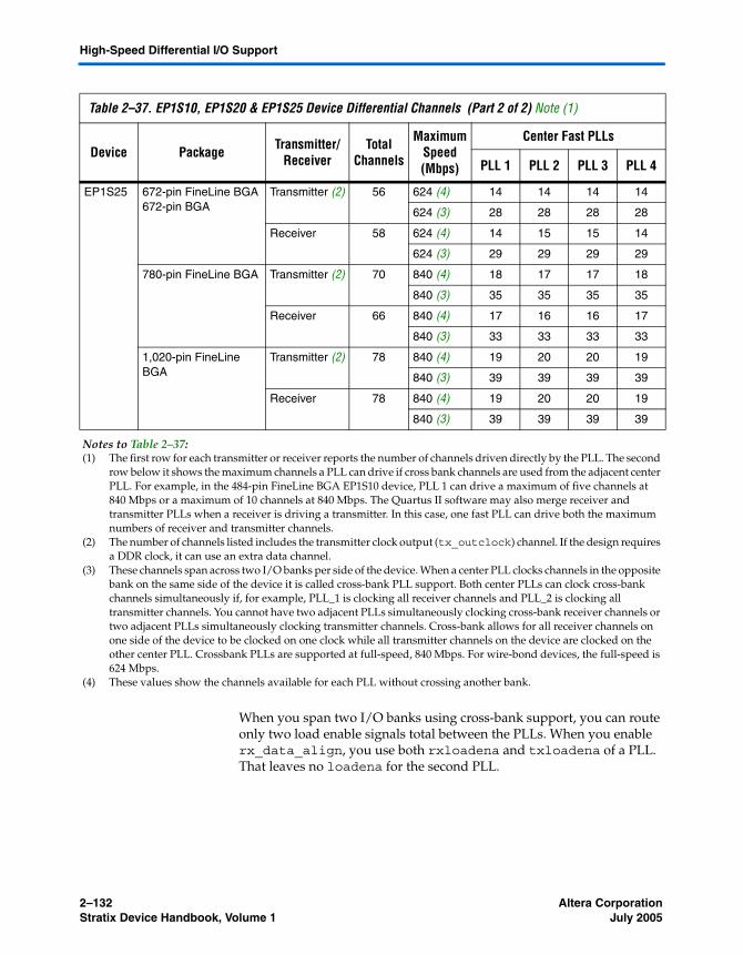
2–132 Altera CorporationStratix Device Handbook, Volume 1 July 2005
High-Speed Differential I/O Support
When you span two I/O banks using cross-bank support, you can route only two load enable signals total between the PLLs. When you enable rx_data_align, you use both rxloadena and txloadena of a PLL. That leaves no loadena for the second PLL.
EP1S25 672-pin FineLine BGA672-pin BGA
Transmitter (2) 56 624 (4) 14 14 14 14
624 (3) 28 28 28 28
Receiver 58 624 (4) 14 15 15 14
624 (3) 29 29 29 29
780-pin FineLine BGA Transmitter (2) 70 840 (4) 18 17 17 18
840 (3) 35 35 35 35
Receiver 66 840 (4) 17 16 16 17
840 (3) 33 33 33 33
1,020-pin FineLine BGA
Transmitter (2) 78 840 (4) 19 20 20 19
840 (3) 39 39 39 39
Receiver 78 840 (4) 19 20 20 19
840 (3) 39 39 39 39
Notes to Table 2–37:(1) The first row for each transmitter or receiver reports the number of channels driven directly by the PLL. The second
row below it shows the maximum channels a PLL can drive if cross bank channels are used from the adjacent center PLL. For example, in the 484-pin FineLine BGA EP1S10 device, PLL 1 can drive a maximum of five channels at 840 Mbps or a maximum of 10 channels at 840 Mbps. The Quartus II software may also merge receiver and transmitter PLLs when a receiver is driving a transmitter. In this case, one fast PLL can drive both the maximum numbers of receiver and transmitter channels.
(2) The number of channels listed includes the transmitter clock output (tx_outclock) channel. If the design requires a DDR clock, it can use an extra data channel.
(3) These channels span across two I/O banks per side of the device. When a center PLL clocks channels in the opposite bank on the same side of the device it is called cross-bank PLL support. Both center PLLs can clock cross-bank channels simultaneously if, for example, PLL_1 is clocking all receiver channels and PLL_2 is clocking all transmitter channels. You cannot have two adjacent PLLs simultaneously clocking cross-bank receiver channels or two adjacent PLLs simultaneously clocking transmitter channels. Cross-bank allows for all receiver channels on one side of the device to be clocked on one clock while all transmitter channels on the device are clocked on the other center PLL. Crossbank PLLs are supported at full-speed, 840 Mbps. For wire-bond devices, the full-speed is 624 Mbps.
(4) These values show the channels available for each PLL without crossing another bank.
Table 2–37. EP1S10, EP1S20 & EP1S25 Device Differential Channels (Part 2 of 2) Note (1)
Device Package Transmitter/Receiver
Total Channels
Maximum Speed (Mbps)
Center Fast PLLs
PLL 1 PLL 2 PLL 3 PLL 4

Altera Corporation 2–133July 2005 Stratix Device Handbook, Volume 1
Stratix Architecture
The only way you can use the rx_data_align is if one of the following is true:
■ The receiver PLL is only clocking receive channels (no resources for the transmitter)
■ If all channels can fit in one I/O bank
Table 2–38. EP1S30 Differential Channels Note (1)
Package Transmitter/Receiver
Total Channels
Maximum Speed (Mbps)
Center Fast PLLs Corner Fast PLLs (2), (3)
PLL1 PLL2 PLL3 PLL4 PLL7 PLL8 PLL9 PLL10
780-pin FineLine BGA
Transmitter (4)
70 840 18 17 17 18 (6) (6) (6) (6)
840 (5) 35 35 35 35 (6) (6) (6) (6)
Receiver 66 840 17 16 16 17 (6) (6) (6) (6)
840 (5) 33 33 33 33 (6) (6) (6) (6)
956-pin BGA
Transmitter (4)
80 840 19 20 20 19 20 20 20 20
840 (5) 39 39 39 39 20 20 20 20
Receiver 80 840 20 20 20 20 19 20 20 19
840 (5) 40 40 40 40 19 20 20 19
1,020-pin FineLine BGA
Transmitter (4)
80 (2) (7) 840 19 (1)
20 20 19 (1)
20 20 20 20
840 (5),(8) 39 (1)
39 (1)
39 (1)
39 (1)
20 20 20 20
Receiver 80 (2) (7) 840 20 20 20 20 19 (1) 20 20 19 (1)
840 (5),(8) 40 40 40 40 19 (1) 20 20 19 (1)
Table 2–39. EP1S40 Differential Channels (Part 1 of 2) Note (1)
Package Transmitter/Receiver
Total Channels
Maximum Speed (Mbps)
Center Fast PLLs Corner Fast PLLs (2), (3)
PLL1 PLL2 PLL3 PLL4 PLL7 PLL8 PLL9 PLL10
780-pin FineLine BGA
Transmitter (4)
68 840 18 16 16 18 (6) (6) (6) (6)
840 (5) 34 34 34 34 (6) (6) (6) (6)
Receiver 66 840 17 16 16 17 (6) (6) (6) (6)
840 (5) 33 33 33 33 (6) (6) (6) (6)
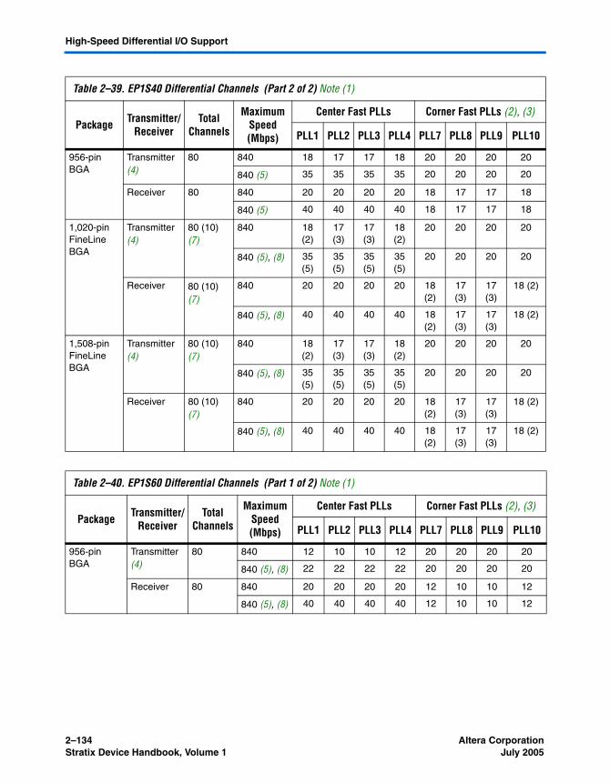
2–134 Altera CorporationStratix Device Handbook, Volume 1 July 2005
High-Speed Differential I/O Support
956-pin BGA
Transmitter (4)
80 840 18 17 17 18 20 20 20 20
840 (5) 35 35 35 35 20 20 20 20
Receiver 80 840 20 20 20 20 18 17 17 18
840 (5) 40 40 40 40 18 17 17 18
1,020-pin FineLine BGA
Transmitter (4)
80 (10) (7)
840 18 (2)
17 (3)
17 (3)
18 (2)
20 20 20 20
840 (5), (8) 35 (5)
35 (5)
35 (5)
35 (5)
20 20 20 20
Receiver 80 (10)
(7)840 20 20 20 20 18
(2)17 (3)
17 (3)
18 (2)
840 (5), (8) 40 40 40 40 18 (2)
17 (3)
17 (3)
18 (2)
1,508-pin FineLine BGA
Transmitter (4)
80 (10) (7)
840 18 (2)
17 (3)
17 (3)
18 (2)
20 20 20 20
840 (5), (8) 35 (5)
35 (5)
35 (5)
35 (5)
20 20 20 20
Receiver 80 (10) (7)
840 20 20 20 20 18 (2)
17 (3)
17 (3)
18 (2)
840 (5), (8) 40 40 40 40 18 (2)
17 (3)
17 (3)
18 (2)
Table 2–40. EP1S60 Differential Channels (Part 1 of 2) Note (1)
Package Transmitter/Receiver
Total Channels
Maximum Speed (Mbps)
Center Fast PLLs Corner Fast PLLs (2), (3)
PLL1 PLL2 PLL3 PLL4 PLL7 PLL8 PLL9 PLL10
956-pinBGA
Transmitter (4)
80 840 12 10 10 12 20 20 20 20
840 (5), (8) 22 22 22 22 20 20 20 20
Receiver 80 840 20 20 20 20 12 10 10 12
840 (5), (8) 40 40 40 40 12 10 10 12
Table 2–39. EP1S40 Differential Channels (Part 2 of 2) Note (1)
Package Transmitter/Receiver
Total Channels
Maximum Speed (Mbps)
Center Fast PLLs Corner Fast PLLs (2), (3)
PLL1 PLL2 PLL3 PLL4 PLL7 PLL8 PLL9 PLL10
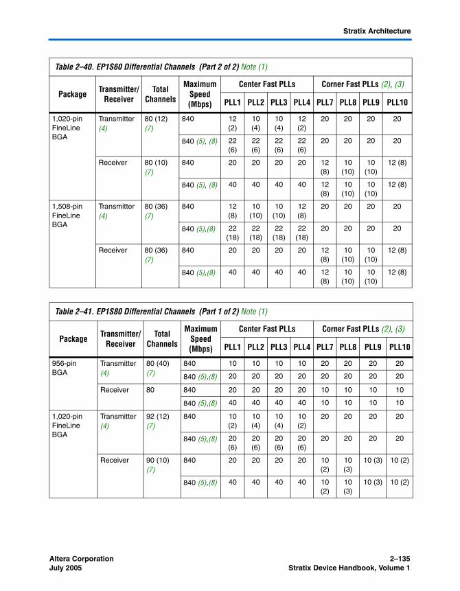
Altera Corporation 2–135July 2005 Stratix Device Handbook, Volume 1
Stratix Architecture
1,020-pin FineLine BGA
Transmitter (4)
80 (12) (7)
840 12 (2)
10 (4)
10 (4)
12 (2)
20 20 20 20
840 (5), (8) 22 (6)
22 (6)
22 (6)
22 (6)
20 20 20 20
Receiver 80 (10) (7)
840 20 20 20 20 12 (8)
10 (10)
10 (10)
12 (8)
840 (5), (8) 40 40 40 40 12 (8)
10 (10)
10 (10)
12 (8)
1,508-pin FineLine BGA
Transmitter (4)
80 (36) (7)
840 12 (8)
10 (10)
10 (10)
12 (8)
20 20 20 20
840 (5),(8) 22 (18)
22 (18)
22 (18)
22 (18)
20 20 20 20
Receiver 80 (36) (7)
840 20 20 20 20 12 (8)
10 (10)
10 (10)
12 (8)
840 (5),(8) 40 40 40 40 12 (8)
10 (10)
10 (10)
12 (8)
Table 2–41. EP1S80 Differential Channels (Part 1 of 2) Note (1)
Package Transmitter/Receiver
Total Channels
Maximum Speed (Mbps)
Center Fast PLLs Corner Fast PLLs (2), (3)
PLL1 PLL2 PLL3 PLL4 PLL7 PLL8 PLL9 PLL10
956-pin BGA
Transmitter (4)
80 (40) (7)
840 10 10 10 10 20 20 20 20
840 (5),(8) 20 20 20 20 20 20 20 20
Receiver 80 840 20 20 20 20 10 10 10 10
840 (5),(8) 40 40 40 40 10 10 10 10
1,020-pin FineLine BGA
Transmitter (4)
92 (12) (7)
840 10 (2)
10 (4)
10 (4)
10 (2)
20 20 20 20
840 (5),(8) 20 (6)
20 (6)
20 (6)
20 (6)
20 20 20 20
Receiver 90 (10) (7)
840 20 20 20 20 10 (2)
10 (3)
10 (3) 10 (2)
840 (5),(8) 40 40 40 40 10 (2)
10 (3)
10 (3) 10 (2)
Table 2–40. EP1S60 Differential Channels (Part 2 of 2) Note (1)
Package Transmitter/Receiver
Total Channels
Maximum Speed (Mbps)
Center Fast PLLs Corner Fast PLLs (2), (3)
PLL1 PLL2 PLL3 PLL4 PLL7 PLL8 PLL9 PLL10

2–136 Altera CorporationStratix Device Handbook, Volume 1 July 2005
High-Speed Differential I/O Support
The high-speed differential I/O circuitry supports the following high speed I/O interconnect standards and applications:
■ UTOPIA IV■ SPI-4 Phase 2 (POS-PHY Level 4)■ SFI-4■ 10G Ethernet XSBI
1,508-pin FineLine BGA
Transmitter (4)
80 (72) (7)
840 10 (10)
10 (10)
10 (10)
10 (10)
20 (8)
20 (8)
20 (8) 20 (8)
840 (5),(8) 20 (20)
20 (20)
20 (20)
20 (20)
20 (8)
20 (8)
20 (8) 20 (8)
Receiver 80 (56) (7)
840 20 20 20 20 10 (14)
10 (14)
10 (14)
10 (14)
840 (5),(8) 40 40 40 40 10 (14)
10 (14)
10 (14)
10 (14)
Notes to Tables 2–38 through 2–41:(1) The first row for each transmitter or receiver reports the number of channels driven directly by the PLL. The second
row below it shows the maximum channels a PLL can drive if cross bank channels are used from the adjacent center PLL. For example, in the 780-pin FineLine BGA EP1S30 device, PLL 1 can drive a maximum of 18 transmitter channels at 840 Mbps or a maximum of 35 transmitter channels at 840 Mbps. The Quartus II software may also merge transmitter and receiver PLLs when a receiver is driving a transmitter. In this case, one fast PLL can drive both the maximum numbers of receiver and transmitter channels.
(2) Some of the channels accessible by the center fast PLL and the channels accessible by the corner fast PLL overlap. Therefore, the total number of channels is not the addition of the number of channels accessible by PLLs 1, 2, 3, and 4 with the number of channels accessible by PLLs 7, 8, 9, and 10. For more information on which channels overlap, see the Stratix device pin-outs at www.altera.com.
(3) The corner fast PLLs in this device support a data rate of 840 Mbps for channels labeled “high” speed in the device pin-outs at www.altera.com.
(4) The numbers of channels listed include the transmitter clock output (tx_outclock) channel. An extra data channel can be used if a DDR clock is needed.
(5) These channels span across two I/O banks per side of the device. When a center PLL clocks channels in the opposite bank on the same side of the device it is called cross-bank PLL support. Both center PLLs can clock cross-bank channels simultaneously if say PLL_1 is clocking all receiver channels and PLL_2 is clocking all transmitter channels. You cannot have two adjacent PLLs simultaneously clocking cross-bank receiver channels or two adjacent PLLs simultaneously clocking transmitter channels. Cross-bank allows for all receiver channels on one side of the device to be clocked on one clock while all transmitter channels on the device are clocked on the other center PLL. Crossbank PLLs are supported at full-speed, 840 Mbps. For wire-bond devices, the full-speed is 624 Mbps.
(6) PLLs 7, 8, 9, and 10 are not available in this device.(7) The number in parentheses is the number of slow-speed channels, guaranteed to operate at up to 462 Mbps. These
channels are independent of the high-speed differential channels. For the location of these channels, see the device pin-outs at www.altera.com.
(8) See the Stratix device pin-outs at www.altera.com. Channels marked “high” speed are 840 MBps and “low” speed channels are 462 MBps.
Table 2–41. EP1S80 Differential Channels (Part 2 of 2) Note (1)
Package Transmitter/Receiver
Total Channels
Maximum Speed (Mbps)
Center Fast PLLs Corner Fast PLLs (2), (3)
PLL1 PLL2 PLL3 PLL4 PLL7 PLL8 PLL9 PLL10
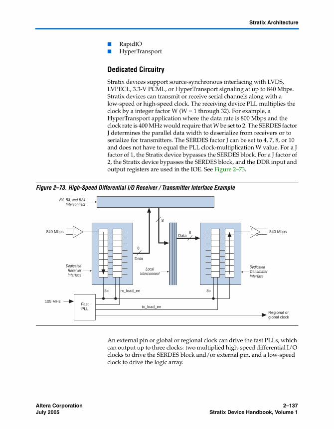
Altera Corporation 2–137July 2005 Stratix Device Handbook, Volume 1
Stratix Architecture
■ RapidIO■ HyperTransport
Dedicated Circuitry
Stratix devices support source-synchronous interfacing with LVDS, LVPECL, 3.3-V PCML, or HyperTransport signaling at up to 840 Mbps. Stratix devices can transmit or receive serial channels along with a low-speed or high-speed clock. The receiving device PLL multiplies the clock by a integer factor W (W = 1 through 32). For example, a HyperTransport application where the data rate is 800 Mbps and the clock rate is 400 MHz would require that W be set to 2. The SERDES factor J determines the parallel data width to deserialize from receivers or to serialize for transmitters. The SERDES factor J can be set to 4, 7, 8, or 10 and does not have to equal the PLL clock-multiplication W value. For a J factor of 1, the Stratix device bypasses the SERDES block. For a J factor of 2, the Stratix device bypasses the SERDES block, and the DDR input and output registers are used in the IOE. See Figure 2–73.
Figure 2–73. High-Speed Differential I/O Receiver / Transmitter Interface Example
An external pin or global or regional clock can drive the fast PLLs, which can output up to three clocks: two multiplied high-speed differential I/O clocks to drive the SERDES block and/or external pin, and a low-speed clock to drive the logic array.
+–
8
Data
Data
FastPLL
105 MHz
8×
840 Mbps
DedicatedReceiverInterface
DedicatedTransmitterInterface
R4, R8, and R24Interconnect
LocalInterconnect
8+–
8×
840 Mbps
tx_load_en
rx_load_en
Regional orglobal clock
8

2–138 Altera CorporationStratix Device Handbook, Volume 1 July 2005
High-Speed Differential I/O Support
The Quartus II MegaWizard® Plug-In Manager only allows the implementation of up to 20 receiver or 20 transmitter channels for each fast PLL. These channels operate at up to 840 Mbps. The receiver and transmitter channels are interleaved such that each I/O bank on the left and right side of the device has one receiver channel and one transmitter channel per LAB row. Figure 2–74 shows the fast PLL and channel layout in EP1S10, EP1S20, and EP1S25 devices. Figure 2–75 shows the fast PLL and channel layout in the EP1S30 to EP1S80 devices.
Figure 2–74. Fast PLL & Channel Layout in the EP1S10, EP1S20 or EP1S25 Devices Note (1)
Notes to Figure 2–74:(1) Wire-bond packages support up to 624 Mbps.(2) See Table 2–41 for the number of channels each device supports.(3) There is a multiplexer here to select the PLL clock source. If a PLL uses this multiplexer to clock channels outside of
its bank quadrant, those clocked channels support up to 840 Mbps for “high” speed channels and 462 Mbps for “low” speed channels, as labeled in the device pin-outs at www.altera.com.
Transmitter
Receiver
Transmitter
Receiver
CLKIN
CLKIN
Transmitter
Receiver
Transmitter
Receiver
CLKIN
CLKINFast
PLL 1
FastPLL 2
(3)
FastPLL 4
FastPLL 3
(3)
Up to 20 Receiver and Transmitter Channels (2)
Up to 20 Receiver and Transmitter Channels (2)
Up to 20 Receiver and Transmitter Channels (2)
Up to 20 Receiver and Transmitter Channels (2)

Altera Corporation 2–139July 2005 Stratix Device Handbook, Volume 1
Stratix Architecture
Figure 2–75. Fast PLL & Channel Layout in the EP1S30 to EP1S80 Devices Note (1)
Notes to Figure 2–75:(1) Wire-bond packages support up to 624 Mbps.(2) See Table 2–38 through 2–41 for the number of channels each device supports.(3) There is a multiplexer here to select the PLL clock source. If a PLL uses this multiplexer to clock channels outside of
its bank quadrant, those clocked channels support up to 840 Mbps for “high” speed channels and 462 Mbps for “low” speed channels as labeled in the device pin-outs at www.altera.com.
Transmitter
Receiver
Transmitter
Receiver
CLKIN
FPLL7CLK
Transmitter
Receiver
Transmitter
Receiver
CLKIN
FPLL10CLK
Transmitter
Receiver
Transmitter
Receiver
FPLL9CLK
CLKIN
FastPLL 7
FastPLL 1
Up to 20 Receiver and 20 Transmitter
Channels in 20 Rows (2)
Transmitter
Receiver
Transmitter
Receiver
FPLL8CLK
CLKINFast
PLL 2
FastPLL 8
Up to 20 Receiver and 20 Transmitter
Channels in 20 Rows (2)
Up to 20 Receiver and 20 Transmitter
Channels in 20 Rows (2)
Up to 20 Receiver and 20 Transmitter
Channels in 20 Rows (2)
(3) (3)
FastPLL 10
FastPLL 4
FastPLL 3
FastPLL 9

2–140 Altera CorporationStratix Device Handbook, Volume 1 July 2005
Power Sequencing & Hot Socketing
The transmitter external clock output is transmitted on a data channel. The txclk pin for each bank is located in between data transmitter pins. For ×1 clocks (e.g., 622 Mbps, 622 MHz), the high-speed PLL clock bypasses the SERDES to drive the output pins. For half-rate clocks (e.g., 622 Mbps, 311 MHz) or any other even-numbered factor such as 1/4, 1/7, 1/8, or 1/10, the SERDES automatically generates the clock in the Quartus II software.
For systems that require more than four or eight high-speed differential I/O clock domains, a SERDES bypass implementation is possible using IOEs.
Byte Alignment
For high-speed source synchronous interfaces such as POS-PHY 4, XSBI, RapidIO, and HyperTransport technology, the source synchronous clock rate is not a byte- or SERDES-rate multiple of the data rate. Byte alignment is necessary for these protocols since the source synchronous clock does not provide a byte or word boundary since the clock is one half the data rate, not one eighth. The Stratix device’s high-speed differential I/O circuitry provides dedicated data realignment circuitry for user-controlled byte boundary shifting. This simplifies designs while saving LE resources. An input signal to each fast PLL can stall deserializer parallel data outputs by one bit period. You can use an LE-based state machine to signal the shift of receiver byte boundaries until a specified pattern is detected to indicate byte alignment.
Power Sequencing & Hot Socketing
Because Stratix devices can be used in a mixed-voltage environment, they have been designed specifically to tolerate any possible power-up sequence. Therefore, the VCCIO and VCCINT power supplies may be powered in any order.
Although you can power up or down the VCCIO and VCCINT power supplies in any sequence, you should not power down any I/O banks that contain configuration pins while leaving other I/O banks powered on. For power up and power down, all supplies (VCCINT and all VCCIO power planes) must be powered up and down within 100 ms of each other. This prevents I/O pins from driving out.
Signals can be driven into Stratix devices before and during power up without damaging the device. In addition, Stratix devices do not drive out during power up. Once operating conditions are reached and the device is configured, Stratix devices operate as specified by the user. For more information, see Hot Socketing in the Selectable I/O Standards in Stratix & Stratix GX Devices chapter in the Stratix Device Handbook, Volume 2.

Altera Corporation 3–1July 2005
3. Configuration & Testing
IEEE Std. 1149.1 (JTAG) Boundary-Scan Support
All Stratix® devices provide JTAG BST circuitry that complies with the IEEE Std. 1149.1a-1990 specification. JTAG boundary-scan testing can be performed either before or after, but not during configuration. Stratix devices can also use the JTAG port for configuration together with either the Quartus® II software or hardware using either Jam Files (.jam) or Jam Byte-Code Files (.jbc).
Stratix devices support IOE I/O standard setting reconfiguration through the JTAG BST chain. The JTAG chain can update the I/O standard for all input and output pins any time before or during user mode through the CONFIG_IO instruction. You can use this ability for JTAG testing before configuration when some of the Stratix pins drive or receive from other devices on the board using voltage-referenced standards. Since the Stratix device may not be configured before JTAG testing, the I/O pins may not be configured for appropriate electrical standards for chip-to-chip communication. Programming those I/O standards via JTAG allows you to fully test the I/O connection to other devices.
The enhanced PLL reconfiguration bits are part of the JTAG chain before configuration and after power-up. After device configuration, the PLL reconfiguration bits are not part of the JTAG chain.
The JTAG pins support 1.5-V/1.8-V or 2.5-V/3.3-V I/O standards. The TDO pin voltage is determined by the VCCIO of the bank where it resides. The VCCSEL pin selects whether the JTAG inputs are 1.5-V, 1.8-V, 2.5-V, or 3.3-V compatible.
Stratix devices also use the JTAG port to monitor the logic operation of the device with the SignalTap® II embedded logic analyzer. Stratix devices support the JTAG instructions shown in Table 3–1.
The Quartus II software has an Auto Usercode feature where you can choose to use the checksum value of a programming file as the JTAG user code. If selected, the checksum is automatically loaded to the USERCODE register. In the Settings dialog box in the Assignments menu, click Device & Pin Options, then General, and then turn on the Auto Usercode option.
S51003-1.3
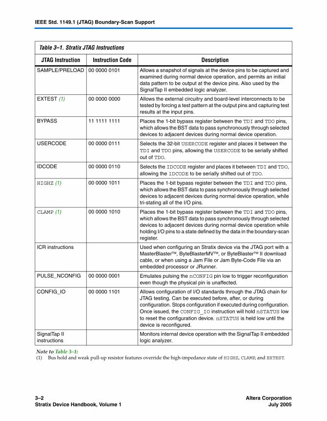
3–2 Altera CorporationStratix Device Handbook, Volume 1 July 2005
IEEE Std. 1149.1 (JTAG) Boundary-Scan Support
Table 3–1. Stratix JTAG Instructions
JTAG Instruction Instruction Code Description
SAMPLE/PRELOAD 00 0000 0101 Allows a snapshot of signals at the device pins to be captured and examined during normal device operation, and permits an initial data pattern to be output at the device pins. Also used by the SignalTap II embedded logic analyzer.
EXTEST (1) 00 0000 0000 Allows the external circuitry and board-level interconnects to be tested by forcing a test pattern at the output pins and capturing test results at the input pins.
BYPASS 11 1111 1111 Places the 1-bit bypass register between the TDI and TDO pins, which allows the BST data to pass synchronously through selected devices to adjacent devices during normal device operation.
USERCODE 00 0000 0111 Selects the 32-bit USERCODE register and places it between the TDI and TDO pins, allowing the USERCODE to be serially shifted out of TDO.
IDCODE 00 0000 0110 Selects the IDCODE register and places it between TDI and TDO, allowing the IDCODE to be serially shifted out of TDO.
HIGHZ (1) 00 0000 1011 Places the 1-bit bypass register between the TDI and TDO pins, which allows the BST data to pass synchronously through selected devices to adjacent devices during normal device operation, while tri-stating all of the I/O pins.
CLAMP (1) 00 0000 1010 Places the 1-bit bypass register between the TDI and TDO pins, which allows the BST data to pass synchronously through selected devices to adjacent devices during normal device operation while holding I/O pins to a state defined by the data in the boundary-scan register.
ICR instructions Used when configuring an Stratix device via the JTAG port with a MasterBlasterTM, ByteBlasterMVTM, or ByteBlasterTM II download cable, or when using a Jam File or Jam Byte-Code File via an embedded processor or JRunner.
PULSE_NCONFIG 00 0000 0001 Emulates pulsing the nCONFIG pin low to trigger reconfiguration even though the physical pin is unaffected.
CONFIG_IO 00 0000 1101 Allows configuration of I/O standards through the JTAG chain for JTAG testing. Can be executed before, after, or during configuration. Stops configuration if executed during configuration. Once issued, the CONFIG_IO instruction will hold nSTATUS low to reset the configuration device. nSTATUS is held low until the device is reconfigured.
SignalTap II instructions
Monitors internal device operation with the SignalTap II embedded logic analyzer.
Note to Table 3–1:(1) Bus hold and weak pull-up resistor features override the high-impedance state of HIGHZ, CLAMP, and EXTEST.

Altera Corporation 3–3July 2005 Stratix Device Handbook, Volume 1
Configuration & Testing
The Stratix device instruction register length is 10 bits and the USERCODE register length is 32 bits. Tables 3–2 and 3–3 show the boundary-scan register length and device IDCODE information for Stratix devices.
Table 3–2. Stratix Boundary-Scan Register Length
Device Boundary-Scan Register Length
EP1S10 1,317
EP1S20 1,797
EP1S25 2,157
EP1S30 2,253
EP1S40 2,529
EP1S60 3,129
EP1S80 3,777
Table 3–3. 32-Bit Stratix Device IDCODE
Device
IDCODE (32 Bits) (1)
Version (4 Bits) Part Number (16 Bits) Manufacturer Identity (11 Bits) LSB (1 Bit) (2)
EP1S10 0000 0010 0000 0000 0001 000 0110 1110 1
EP1S20 0000 0010 0000 0000 0010 000 0110 1110 1
EP1S25 0000 0010 0000 0000 0011 000 0110 1110 1
EP1S30 0000 0010 0000 0000 0100 000 0110 1110 1
EP1S40 0000 0010 0000 0000 0101 000 0110 1110 1
EP1S60 0000 0010 0000 0000 0110 000 0110 1110 1
EP1S80 0000 0010 0000 0000 0111 000 0110 1110 1
Notes to Tables 3–2 and 3–3:(1) The most significant bit (MSB) is on the left.(2) The IDCODE’s least significant bit (LSB) is always 1.

3–4 Altera CorporationStratix Device Handbook, Volume 1 July 2005
IEEE Std. 1149.1 (JTAG) Boundary-Scan Support
Figure 3–1 shows the timing requirements for the JTAG signals.
Figure 3–1. Stratix JTAG Waveforms
Table 3–4 shows the JTAG timing parameters and values for Stratix devices.
Table 3–4. Stratix JTAG Timing Parameters & Values
Symbol Parameter Min Max Unit
tJCP TCK clock period 100 ns
tJCH TCK clock high time 50 ns
tJCL TCK clock low time 50 ns
tJPSU JTAG port setup time 20 ns
tJPH JTAG port hold time 45 ns
tJPCO JTAG port clock to output 25 ns
tJPZX JTAG port high impedance to valid output 25 ns
tJPXZ JTAG port valid output to high impedance 25 ns
tJSSU Capture register setup time 20 ns
tJSH Capture register hold time 45 ns
tJSCO Update register clock to output 35 ns
tJSZX Update register high impedance to valid output 35 ns
tJSXZ Update register valid output to high impedance 35 ns
TDO
TCK
tJPZX tJPCO
tJPH
t JPXZ
tJCP
tJPSU t JCL tJCH
TDI
TMS
Signalto Be
Captured
Signalto Be
Driven
tJSZX
tJSSU tJSH
tJSCO tJSXZ

Altera Corporation 3–5July 2005 Stratix Device Handbook, Volume 1
Configuration & Testing
1 Stratix, Stratix II, Cyclone®, and Cyclone II devices must be within the first 17 devices in a JTAG chain. All of these devices have the same JTAG controller. If any of the Stratix, Stratix II, Cyclone, and Cyclone II devices are in the 18th or after they will fail configuration. This does not affect SignalTap II.
f For more information on JTAG, see the following documents:
■ AN 39: IEEE Std. 1149.1 (JTAG) Boundary-Scan Testing in Altera Devices ■ Jam Programming & Test Language Specification
SignalTap II Embedded Logic Analyzer
Stratix devices feature the SignalTap II embedded logic analyzer, which monitors design operation over a period of time through the IEEE Std. 1149.1 (JTAG) circuitry. You can analyze internal logic at speed without bringing internal signals to the I/O pins. This feature is particularly important for advanced packages, such as FineLine BGA® packages, because it can be difficult to add a connection to a pin during the debugging process after a board is designed and manufactured.
Configuration The logic, circuitry, and interconnects in the Stratix architecture are configured with CMOS SRAM elements. Altera® devices are reconfigurable. Because every device is tested with a high-coverage production test program, you do not have to perform fault testing and can focus on simulation and design verification.
Stratix devices are configured at system power-up with data stored in an Altera serial configuration device or provided by a system controller. Altera offers in-system programmability (ISP)-capable configuration devices that configure Stratix devices via a serial data stream. Stratix devices can be configured in under 100 ms using 8-bit parallel data at 100 MHz. The Stratix device’s optimized interface allows microprocessors to configure it serially or in parallel, and synchronously or asynchronously. The interface also enables microprocessors to treat Stratix devices as memory and configure them by writing to a virtual memory location, making reconfiguration easy. After a Stratix device has been configured, it can be reconfigured in-circuit by resetting the device and loading new data. Real-time changes can be made during system operation, enabling innovative reconfigurable computing applications.
Operating Modes
The Stratix architecture uses SRAM configuration elements that require configuration data to be loaded each time the circuit powers up. The process of physically loading the SRAM data into the device is called configuration. During initialization, which occurs immediately after
3–6 Altera CorporationStratix Device Handbook, Volume 1 July 2005
Configuration
configuration, the device resets registers, enables I/O pins, and begins to operate as a logic device. The I/O pins are tri-stated during power-up, and before and during configuration. Together, the configuration and initialization processes are called command mode. Normal device operation is called user mode.
SRAM configuration elements allow Stratix devices to be reconfigured in-circuit by loading new configuration data into the device. With real-time reconfiguration, the device is forced into command mode with a device pin. The configuration process loads different configuration data, reinitializes the device, and resumes user-mode operation. You can perform in-field upgrades by distributing new configuration files either within the system or remotely.
PORSEL is a dedicated input pin used to select POR delay times of 2 ms or 100 ms during power-up. When the PORSEL pin is connected to ground, the POR time is 100 ms; when the PORSEL pin is connected to VCC, the POR time is 2 ms.
The nIO_PULLUP pin enables a built-in weak pull-up resistor to pull all user I/O pins to VCCIO before and during device configuration. If nIO_PULLUP is connected to VCC during configuration, the weak pull-ups on all user I/O pins are disabled. If connected to ground, the pull-ups are enabled during configuration. The nIO_PULLUP pin can be pulled to 1.5, 1.8, 2.5, or 3.3 V for a logic level high.
VCCSEL is a dedicated input that is used to choose whether all dedicated configuration and JTAG input pins can accept 1.5 V/1.8 V or 2.5 V/3.3 V during configuration. A logic low sets 3.3 V/2.5 V, and a logic high sets 1.8 V/1.5 V. VCCSEL affects the following pins: TDI, TMS, TCK, TRST, MSEL0, MSEL1, MSEL2, nCONFIG, nCE, DCLK, PLL_ENA, CONF_DONE, nSTATUS. The VCCSEL pin can be pulled to 1.5, 1.8, 2.5, or 3.3 V for a logic level high.
The VCCSEL signal does not control the dual-purpose configuration pins such as the DATA[7..0] and PPA pins (nWS, nRS, CS, nCS, and RDYnBSY). During configuration, these dual-purpose pins will drive out voltage levels corresponding to the VCCIO supply voltage that powers the I/O bank containing the pin. After configuration, the dual-purpose pins use I/O standards specified in the user design.
TDO and nCEO drive out at the same voltages as the VCCIO supply that powers the I/O bank containing the pin. Users must select the VCCIO supply for bank containing TDO accordingly. For example, when using the ByteBlaster™ MV cable, the VCCIO for the bank containing TDO must be powered up at 3.3 V.

Altera Corporation 3–7July 2005 Stratix Device Handbook, Volume 1
Configuration & Testing
Configuring Stratix FPGAs with JRunner
JRunner is a software driver that configures Altera FPGAs, including Stratix FPGAs, through the ByteBlaster II or ByteBlasterMV cables in JTAG mode. The programming input file supported is in Raw Binary File (.rbf) format. JRunner also requires a Chain Description File (.cdf) generated by the Quartus II software. JRunner is targeted for embedded JTAG configuration. The source code is developed for the Windows NT operating system (OS), but can be customized to run on other platforms. For more information on the JRunner software driver, see the JRunner Software Driver: An Embedded Solution to the JTAG Configuration White Paper and the source files on the Altera web site (www.altera.com).
Configuration Schemes
You can load the configuration data for a Stratix device with one of five configuration schemes (see Table 3–5), chosen on the basis of the target application. You can use a configuration device, intelligent controller, or the JTAG port to configure a Stratix device. A configuration device can automatically configure a Stratix device at system power-up.
Multiple Stratix devices can be configured in any of five configuration schemes by connecting the configuration enable (nCE) and configuration enable output (nCEO) pins on each device.
Partial Reconfiguration
The enhanced PLLs within the Stratix device family support partial reconfiguration of their multiply, divide, and time delay settings without reconfiguring the entire device. You can use either serial data from the logic array or regular I/O pins to program the PLL’s counter settings in a serial chain. This option provides considerable flexibility for frequency
Table 3–5. Data Sources for Configuration
Configuration Scheme Data Source
Configuration device Enhanced or EPC2 configuration device
Passive serial (PS) MasterBlaster, ByteBlasterMV, or ByteBlaster II download cable or serial data source
Passive parallel asynchronous (PPA)
Parallel data source
Fast passive parallel Parallel data source
JTAG MasterBlaster, ByteBlasterMV, or ByteBlaster II download cable, a microprocessor with a Jam or JBC file, or JRunner

3–8 Altera CorporationStratix Device Handbook, Volume 1 July 2005
Configuration
synthesis, allowing real-time variation of the PLL frequency and delay. The rest of the device is functional while reconfiguring the PLL. See the Stratix Architecture chapter of the Stratix Device Handbook, Volume 1 for more information on Stratix PLLs.
Remote Update Configuration Modes
Stratix devices also support remote configuration using an Altera enhanced configuration device (e.g., EPC16, EPC8, and EPC4 devices) with page mode selection. Factory configuration data is stored in the default page of the configuration device. This is the default configuration that contains the design required to control remote updates and handle or recover from errors. You write the factory configuration once into the flash memory or configuration device. Remote update data can update any of the remaining pages of the configuration device. If there is an error or corruption in a remote update configuration, the configuration device reverts back to the factory configuration information.
There are two remote configuration modes: remote and local configuration. You can use the remote update configuration mode for all three configuration modes: serial, parallel synchronous, and parallel asynchronous. Configuration devices (for example, EPC16 devices) only support serial and parallel synchronous modes. Asynchronous parallel mode allows remote updates when an intelligent host is used to configure the Stratix device. This host must support page mode settings similar to an EPC16 device.
Remote Update Mode
When the Stratix device is first powered up in remote update programming mode, it loads the configuration located at page address “000.” The factory configuration should always be located at page address “000,” and should never be remotely updated. The factory configuration contains the required logic to perform the following operations:
■ Determine the page address/load location for the next application’s configuration data
■ Recover from a previous configuration error■ Receive new configuration data and write it into the configuration
device
The factory configuration is the default and takes control if an error occurs while loading the application configuration.

Altera Corporation 3–9July 2005 Stratix Device Handbook, Volume 1
Configuration & Testing
While in the factory configuration, the factory-configuration logic performs the following operations:
■ Loads a remote update-control register to determine the page address of the new application configuration
■ Determines whether to enable a user watchdog timer for the application configuration
■ Determines what the watchdog timer setting should be if it is enabled
The user watchdog timer is a counter that must be continually reset within a specific amount of time in the user mode of an application configuration to ensure that valid configuration occurred during a remote update. Only valid application configurations designed for remote update can reset the user watchdog timer in user mode. If a valid application configuration does not reset the user watchdog timer in a specific amount of time, the timer updates a status register and loads the factory configuration. The user watchdog timer is automatically disabled for factory configurations.
If an error occurs in loading the application configuration, the configuration logic writes a status register to specify the cause of the error. Once this occurs, the Stratix device automatically loads the factory configuration, which reads the status register and determines the reason for reconfiguration. Based on the reason, the factory configuration will take appropriate steps and will write the remote update control register to specify the next application configuration page to be loaded.
When the Stratix device successfully loads the application configuration, it enters into user mode. The Stratix device then executes the main application of the user. Intellectual property (IP), such as a Nios® (16-bit ISA) and Nios® II (32-bit ISA) embedded processors, can help the Stratix device determine when remote update is coming. The Nios embedded processor or user logic receives incoming data, writes it to the configuration device, and loads the factory configuration. The factory configuration will read the remote update status register and determine the valid application configuration to load. Figure 3–2 shows the Stratix remote update. Figure 3–3 shows the transition diagram for remote update mode.

3–10 Altera CorporationStratix Device Handbook, Volume 1 July 2005
Configuration
Figure 3–2. Stratix Device Remote Update
Note to Figure 3–2:(1) When the Stratix device is configured with the factory configuration, it can handle update data from EPC16, EPC8,
or EPC4 configuration device pages and point to the next page in the configuration device.
WatchdogTimer
Stratix Device
New RemoteConfiguration Data
ConfigurationDevice
Application Configuration
Application Configuration
Factory Configuration
(1)
Configuration Device UpdatesStratix Device with Factory
Configuration (to Handle Update)or New Application Configuration
Page 7
Page 6
Page 0
Altera Corporation 3–11July 2005 Stratix Device Handbook, Volume 1
Configuration & Testing
Figure 3–3. Remote Update Transition Diagram Notes (1), (2)
Notes to Figure 3–3:(1) Remote update of Application Configuration is controlled by a Nios embedded processor or user logic programmed
in the Factory or Application configurations.(2) Up to seven pages can be specified allowing up to seven different configuration applications.
ConfigurationError
ConfigurationError
Application 1Configuration
ConfigurationError
FactoryConfiguration
Reload anApplication
Reload anApplication
Application nConfiguration
Power-Up

3–12 Altera CorporationStratix Device Handbook, Volume 1 July 2005
Stratix Automated Single Event Upset (SEU) Detection
Local Update Mode
Local update mode is a simplified version of the remote update. This feature is intended for simple systems that need to load a single application configuration immediately upon power up without loading the factory configuration first. Local update designs have only one application configuration to load, so it does not require a factory configuration to determine which application configuration to use. Figure 3–4 shows the transition diagram for local update mode.
Figure 3–4. Local Update Transition Diagram
Stratix Automated Single Event Upset (SEU) Detection
Stratix devices offer on-chip circuitry for automated checking of single event upset (SEU) detection. FPGA devices that operate at high elevations or in close proximity to earth’s North or South Pole require periodic checks to ensure continued data integrity. The error detection cyclic redundancy check (CRC) feature controlled by the Device & Pin Options dialog box in the Quartus II software uses a 32-bit CRC circuit to ensure data reliability and is one of the best options for mitigating SEU.
nCONFIG
nCONFIGConfigurationError
ApplicationConfiguration
ConfigurationError
FactoryConfiguration
Power-Upor nCONFIG

Altera Corporation 3–13July 2005 Stratix Device Handbook, Volume 1
Configuration & Testing
For Stratix, the CRC is computed by the Quartus II software and downloaded into the device as a part of the configuration bit stream. The CRC_ERROR pin reports a soft error when configuration SRAM data is corrupted, triggering device reconfiguration.
Custom-Built Circuitry
Dedicated circuitry is built in the Stratix devices to perform error detection automatically. You can use the built-in dedicated circuitry for error detection using CRC feature in Stratix devices, eliminating the need for external logic. This circuitry will perform error detection automatically when enabled. This error detection circuitry in Stratix devices constantly checks for errors in the configuration SRAM cells while the device is in user mode. You can monitor one external pin for the error and use it to trigger a re-configuration cycle. Select the desired time between checks by adjusting a built-in clock divider.
Software Interface
In the Quartus II software version 4.1 and later, you can turn on the automated error detection CRC feature in the Device & Pin Options dialog box. This dialog box allows you to enable the feature and set the internal frequency of the CRC between 400 kHz to 100 MHz. This controls the rate that the CRC circuitry verifies the internal configuration SRAM bits in the FPGA device.
For more information on CRC, see AN 357: Error Detection Using CRC in Altera FPGA Devices.
Temperature Sensing Diode
Stratix devices include a diode-connected transistor for use as a temperature sensor in power management. This diode is used with an external digital thermometer device such as a MAX1617A or MAX1619 from MAXIM Integrated Products. These devices steer bias current through the Stratix diode, measuring forward voltage and converting this reading to temperature in the form of an 8-bit signed number (7 bits plus sign). The external device’s output represents the junction temperature of the Stratix device and can be used for intelligent power management.
The diode requires two pins (tempdiodep and tempdioden) on the Stratix device to connect to the external temperature-sensing device, as shown in Figure 3–5. The temperature sensing diode is a passive element and therefore can be used before the Stratix device is powered.

3–14 Altera CorporationStratix Device Handbook, Volume 1 July 2005
Temperature Sensing Diode
Figure 3–5. External Temperature-Sensing Diode
Table 3–6 shows the specifications for bias voltage and current of the Stratix temperature sensing diode.
Table 3–6. Temperature-Sensing Diode Electrical Characteristics
Parameter Minimum Typical Maximum Unit
IBIAS high 80 100 120 μA
IBIAS low 8 10 12 μA
VBP – VBN 0.3 0.9 V
VBN 0.7 V
Series resistance 3 W
Stratix Device
Temperature-Sensing Device
tempdiodep
tempdioden

Altera Corporation 3–15July 2005 Stratix Device Handbook, Volume 1
Configuration & Testing
The temperature-sensing diode works for the entire operating range shown in Figure 3–6.
Figure 3–6. Temperature vs. Temperature-Sensing Diode Voltage
0.90
0.85
0.95
0.75
0.65
Voltage(Across Diode)
Temperature ( C)
0.55
0.45
0.60
0.50
0.40
0.70
0.80
–55 –30 –5 20 45 70 95 120
10 μA Bias Current100 μA Bias Current
3–16 Altera CorporationStratix Device Handbook, Volume 1 July 2005
Temperature Sensing Diode

Altera Corporation 4–1January 2006
4. DC & SwitchingCharacteristics
Operating Conditions
Stratix® devices are offered in both commercial and industrial grades. Industrial devices are offered in -6 and -7 speed grades and commercial devices are offered in -5 (fastest), -6, -7, and -8 speed grades. This section specifies the operation conditions for operating junction temperature, VCCINT and VCCIO voltage levels, and input voltage requirements. The voltage specifications in this section are specified at the pins of the device (and not the power supply). If the device operates outside these ranges, then all DC and AC specifications are not guaranteed. Furthermore, the reliability of the device may be affected. The timing parameters in this chapter apply to both commercial and industrial temperature ranges unless otherwise stated.
Tables 4–1 through 4–8 provide information on absolute maximum ratings.
Table 4–1. Stratix Device Absolute Maximum Ratings Notes (1), (2)
Symbol Parameter Conditions Minimum Maximum Unit
VCCINT Supply voltage With respect to ground –0.5 2.4 V
VCCIO –0.5 4.6 V
VI DC input voltage (3) –0.5 4.6 V
IOUT DC output current, per pin –25 40 mA
TSTG Storage temperature No bias –65 150 °C
TJ Junction temperature BGA packages under bias 135 °C
Table 4–2. Stratix Device Recommended Operating Conditions (Part 1 of 2)
Symbol Parameter Conditions Minimum Maximum Unit
VCCINT Supply voltage for internal logic and input buffers
(4) 1.425 1.575 V
S51004-3.4

4–2 Altera CorporationStratix Device Handbook, Volume 1 January 2006
Operating Conditions
VCCIO Supply voltage for output buffers, 3.3-V operation
(4), (5) 3.00 (3.135) 3.60 (3.465) V
Supply voltage for output buffers, 2.5-V operation
(4) 2.375 2.625 V
Supply voltage for output buffers, 1.8-V operation
(4) 1.71 1.89 V
Supply voltage for output buffers, 1.5-V operation
(4) 1.4 1.6 V
VI Input voltage (3), (6) –0.5 4.0 V
VO Output voltage 0 VCCIO V
TJ Operating junction temperature
For commercial use 0 85 °C
For industrial use –40 100 °C
Table 4–3. Stratix Device DC Operating Conditions Note (7) (Part 1 of 2)
Symbol Parameter Conditions Minimum Typical Maximum Unit
II Input pin leakage current
VI = VCCIOmax to 0 V (8) –10 10 μA
IOZ Tri-stated I/O pin leakage current
VO = VCCIOmax to 0 V (8) –10 10 μA
ICC0 VCC supply current (standby) (All memory blocks in power-down mode)
VI = ground, no load, no toggling inputs
mA
EP1S10. VI = ground, no load, no toggling inputs
37 mA
EP1S20. VI = ground, no load, no toggling inputs
65 mA
EP1S25. VI = ground, no load, no toggling inputs
90 mA
EP1S30. VI = ground, no load, no toggling inputs
114 mA
EP1S40. VI = ground, no load, no toggling inputs
145 mA
EP1S60. VI = ground, no load, no toggling inputs
200 mA
EP1S80. VI = ground, no load, no toggling inputs
277 mA
Table 4–2. Stratix Device Recommended Operating Conditions (Part 2 of 2)
Symbol Parameter Conditions Minimum Maximum Unit

Altera Corporation 4–3January 2006 Stratix Device Handbook, Volume 1
DC & Switching Characteristics
RCONF Value of I/O pin pull-up resistor before and during configuration
VCCIO = 3.0 V (9) 20 50 kΩ
VCCIO = 2.375 V (9) 30 80 kΩ
VCCIO = 1.71 V (9) 60 150 kΩ
Table 4–4. LVTTL Specifications
Symbol Parameter Conditions Minimum Maximum Unit
VCCIO Output supply voltage 3.0 3.6 V
VI H High-level input voltage 1.7 4.1 V
VIL Low-level input voltage –0.5 0.7 V
VOH High-level output voltage IOH = –4 to –24 mA (10) 2.4 V
VOL Low-level output voltage IOL = 4 to 24 mA (10) 0.45 V
Table 4–5. LVCMOS Specifications
Symbol Parameter Conditions Minimum Maximum Unit
VCCIO Output supply voltage 3.0 3.6 V
VIH High-level input voltage 1.7 4.1 V
VIL Low-level input voltage –0.5 0.7 V
VOH High-level output voltage VCCIO = 3.0, IOH = –0.1 mA
VCCIO – 0.2 V
VOL Low-level output voltage VCCIO = 3.0,IOL = 0.1 mA
0.2 V
Table 4–6. 2.5-V I/O Specifications
Symbol Parameter Conditions Minimum Maximum Unit
VCCIO Output supply voltage 2.375 2.625 V
VIH High-level input voltage 1.7 4.1 V
VIL Low-level input voltage –0.5 0.7 V
VOH High-level output voltage IOH = –1 mA (10) 2.0 V
VOL Low-level output voltage IOL = 1 mA (10) 0.4 V
Table 4–3. Stratix Device DC Operating Conditions Note (7) (Part 2 of 2)
Symbol Parameter Conditions Minimum Typical Maximum Unit
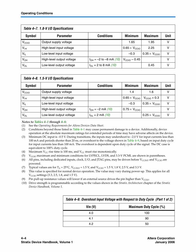
4–4 Altera CorporationStratix Device Handbook, Volume 1 January 2006
Operating Conditions
Table 4–7. 1.8-V I/O Specifications
Symbol Parameter Conditions Minimum Maximum Unit
VCCIO Output supply voltage 1.65 1.95 V
VI H High-level input voltage 0.65 × VCCIO 2.25 V
VIL Low-level input voltage –0.3 0.35 × VCCIO V
VOH High-level output voltage IOH = –2 to –8 mA (10) VCCIO – 0.45 V
VOL Low-level output voltage IOL = 2 to 8 mA (10) 0.45 V
Table 4–8. 1.5-V I/O Specifications
Symbol Parameter Conditions Minimum Maximum Unit
VCCIO Output supply voltage 1.4 1.6 V
VI H High-level input voltage 0.65 × VCCIO VCCIO + 0.3 V
VIL Low-level input voltage –0.3 0.35 × VCCIO V
VOH High-level output voltage IOH = –2 mA (10) 0.75 × VCCIO V
VOL Low-level output voltage IOL = 2 mA (10) 0.25 × VCCIO V
Notes to Tables 4–1 through 4–8:(1) See the Operating Requirements for Altera Devices Data Sheet. (2) Conditions beyond those listed in Table 4–1 may cause permanent damage to a device. Additionally, device
operation at the absolute maximum ratings for extended periods of time may have adverse affects on the device.(3) Minimum DC input is –0.5 V. During transitions, the inputs may undershoot to –2.0 V for input currents less than
100 mA and periods shorter than 20 ns, or overshoot to the voltage shown in Table 4–9, based on input duty cycle for input currents less than 100 mA. The overshoot is dependent upon duty cycle of the signal. The DC case is equivalent to 100% duty cycle.
(4) Maximum VCC rise time is 100 ms, and VCC must rise monotonically.(5) VCCIO maximum and minimum conditions for LVPECL, LVDS, and 3.3-V PCML are shown in parentheses.(6) All pins, including dedicated inputs, clock, I/O, and JTAG pins, may be driven before VCCINT and VCCIO are
powered.(7) Typical values are for TA = 25°C, VCCINT = 1.5 V, and VCCIO = 1.5 V, 1.8 V, 2.5 V, and 3.3 V.(8) This value is specified for normal device operation. The value may vary during power-up. This applies for all
VCCIO settings (3.3, 2.5, 1.8, and 1.5 V).(9) Pin pull-up resistance values will lower if an external source drives the pin higher than VCCIO.(10) Drive strength is programmable according to the values shown in the Stratix Architecture chapter of the Stratix
Device Handbook, Volume 1.
Table 4–9. Overshoot Input Voltage with Respect to Duty Cycle (Part 1 of 2)
Vin (V) Maximum Duty Cycle (%)
4.0 100
4.1 90
4.2 50

Altera Corporation 4–5January 2006 Stratix Device Handbook, Volume 1
DC & Switching Characteristics
Figures 4–1 and 4–2 show receiver input and transmitter output waveforms, respectively, for all differential I/O standards (LVDS, 3.3-V PCML, LVPECL, and HyperTransport technology).
Figure 4–1. Receiver Input Waveforms for Differential I/O Standards
4.3 30
4.4 17
4.5 10
Table 4–9. Overshoot Input Voltage with Respect to Duty Cycle (Part 2 of 2)
Vin (V) Maximum Duty Cycle (%)
Single-Ended Waveform
Differential Waveform
Positive Channel (p) = VIH
Negative Channel (n) = VIL
Ground
VID
VID
VID
VCM
p − n = 0 V
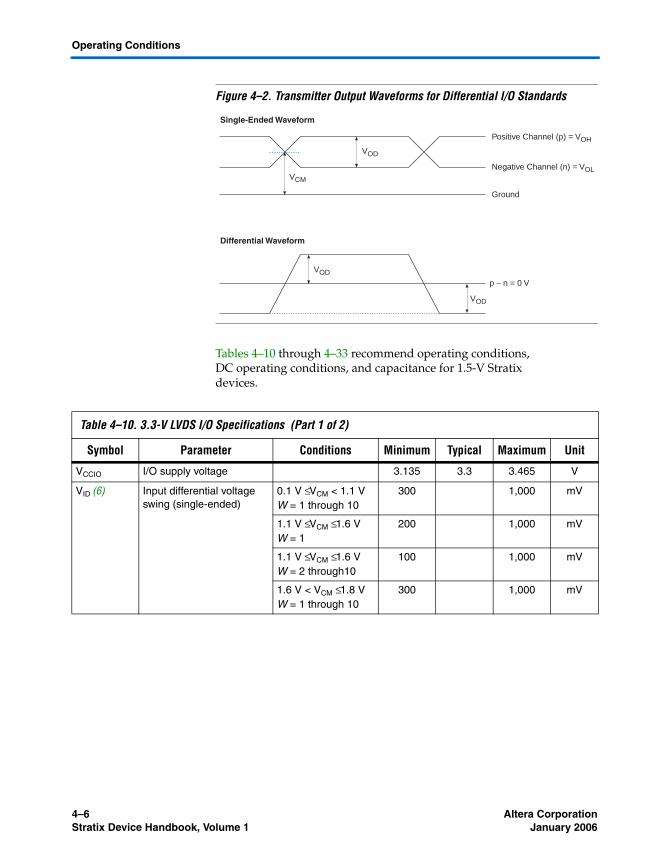
4–6 Altera CorporationStratix Device Handbook, Volume 1 January 2006
Operating Conditions
Figure 4–2. Transmitter Output Waveforms for Differential I/O Standards
Tables 4–10 through 4–33 recommend operating conditions, DC operating conditions, and capacitance for 1.5-V Stratix devices.
Single-Ended Waveform
Differential Waveform
Positive Channel (p) = VOH
Negative Channel (n) = VOL
Ground
VOD
VOD
VOD
p − n = 0 V
VCM
Table 4–10. 3.3-V LVDS I/O Specifications (Part 1 of 2)
Symbol Parameter Conditions Minimum Typical Maximum Unit
VCCIO I/O supply voltage 3.135 3.3 3.465 V
VID (6) Input differential voltage swing (single-ended)
0.1 V ≤ VCM < 1.1 VW = 1 through 10
300 1,000 mV
1.1 V ≤ VCM ≤ 1.6 VW = 1
200 1,000 mV
1.1 V ≤ VCM ≤ 1.6 VW = 2 through10
100 1,000 mV
1.6 V < VCM ≤ 1.8 VW = 1 through 10
300 1,000 mV
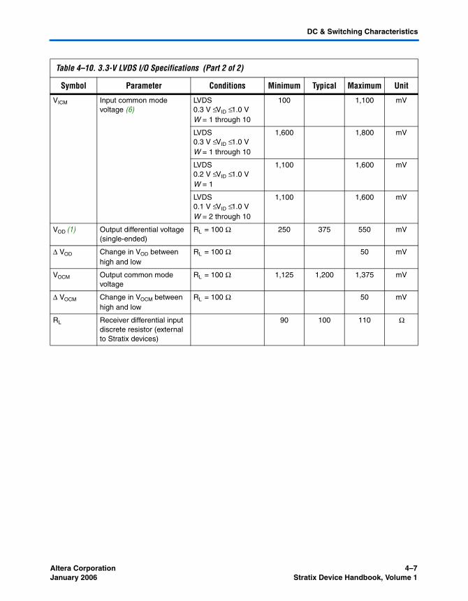
Altera Corporation 4–7January 2006 Stratix Device Handbook, Volume 1
DC & Switching Characteristics
VICM Input common mode voltage (6)
LVDS0.3 V ≤ VID ≤ 1.0 V W = 1 through 10
100 1,100 mV
LVDS0.3 V ≤ VID ≤ 1.0 VW = 1 through 10
1,600 1,800 mV
LVDS0.2 V ≤ VID ≤ 1.0 VW = 1
1,100 1,600 mV
LVDS0.1 V ≤ VID ≤ 1.0 VW = 2 through 10
1,100 1,600 mV
VOD (1) Output differential voltage (single-ended)
RL = 100 Ω 250 375 550 mV
Δ VOD Change in VOD between high and low
RL = 100 Ω 50 mV
VOCM Output common mode voltage
RL = 100 Ω 1,125 1,200 1,375 mV
Δ VOCM Change in VOCM between high and low
RL = 100 Ω 50 mV
RL Receiver differential input discrete resistor (external to Stratix devices)
90 100 110 Ω
Table 4–10. 3.3-V LVDS I/O Specifications (Part 2 of 2)
Symbol Parameter Conditions Minimum Typical Maximum Unit
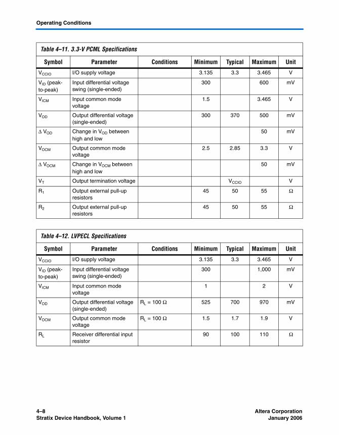
4–8 Altera CorporationStratix Device Handbook, Volume 1 January 2006
Operating Conditions
Table 4–11. 3.3-V PCML Specifications
Symbol Parameter Conditions Minimum Typical Maximum Unit
VCCIO I/O supply voltage 3.135 3.3 3.465 V
VID (peak-to-peak)
Input differential voltage swing (single-ended)
300 600 mV
VICM Input common mode voltage
1.5 3.465 V
VOD Output differential voltage (single-ended)
300 370 500 mV
Δ VOD Change in VOD between high and low
50 mV
VOCM Output common mode voltage
2.5 2.85 3.3 V
Δ VOCM Change in VOCM between high and low
50 mV
VT Output termination voltage VCCIO V
R1 Output external pull-up resistors
45 50 55 Ω
R2 Output external pull-up resistors
45 50 55 Ω
Table 4–12. LVPECL Specifications
Symbol Parameter Conditions Minimum Typical Maximum Unit
VCCIO I/O supply voltage 3.135 3.3 3.465 V
VID (peak-to-peak)
Input differential voltage swing (single-ended)
300 1,000 mV
VICM Input common mode voltage
1 2 V
VOD Output differential voltage (single-ended)
RL = 100 Ω 525 700 970 mV
VOCM Output common mode voltage
RL = 100 Ω 1.5 1.7 1.9 V
RL Receiver differential input resistor
90 100 110 Ω

Altera Corporation 4–9January 2006 Stratix Device Handbook, Volume 1
DC & Switching Characteristics
Table 4–13. HyperTransport Technology Specifications
Symbol Parameter Conditions Minimum Typical Maximum Unit
VCCIO I/O supply voltage 2.375 2.5 2.625 V
VID (peak-to-peak)
Input differential voltage swing (single-ended)
300 900 mV
VICM Input common mode voltage
300 900 mV
VOD Output differential voltage (single-ended)
RL = 100 Ω 380 485 820 mV
Δ VOD Change in VOD between high and low
RL = 100 Ω 50 mV
VOCM Output common mode voltage
RL = 100 Ω 440 650 780 mV
Δ VOCM Change in VOCM between high and low
RL = 100 Ω 50 mV
RL Receiver differential input resistor
90 100 110 Ω
Table 4–14. 3.3-V PCI Specifications
Symbol Parameter Conditions Minimum Typical Maximum Unit
VCCIO Output supply voltage 3.0 3.3 3.6 V
VIH High-level input voltage 0.5 × VCCIO
VCCIO + 0.5
V
VIL Low-level input voltage –0.5 0.3 × VCCIO
V
VOH High-level output voltage IOUT = –500 μA 0.9 × VCCIO
V
VOL Low-level output voltage IOUT = 1,500 μA 0.1 × VCCIO
V

4–10 Altera CorporationStratix Device Handbook, Volume 1 January 2006
Operating Conditions
Table 4–15. PCI-X 1.0 Specifications
Symbol Parameter Conditions Minimum Typical Maximum Unit
VCCIO Output supply voltage 3.0 3.6 V
VIH High-level input voltage 0.5 × VCCIO
VCCIO + 0.5
V
VIL Low-level input voltage –0.5 0.35 × VCCIO
V
VIPU Input pull-up voltage 0.7 × VCCIO
V
VOH High-level output voltage IOUT = –500 μA 0.9 × VCCIO
V
VOL Low-level output voltage IOUT = 1,500 μA 0.1 × VCCIO
V
Table 4–16. GTL+ I/O Specifications
Symbol Parameter Conditions Minimum Typical Maximum Unit
VTT Termination voltage 1.35 1.5 1.65 V
VREF Reference voltage 0.88 1.0 1.12 V
VIH High-level input voltage VREF + 0.1 V
VIL Low-level input voltage VREF – 0.1 V
VOL Low-level output voltage IOL = 34 mA (3) 0.65 V
Table 4–17. GTL I/O Specifications
Symbol Parameter Conditions Minimum Typical Maximum Unit
VTT Termination voltage 1.14 1.2 1.26 V
VREF Reference voltage 0.74 0.8 0.86 V
VIH High-level input voltage VREF + 0.05
V
VIL Low-level input voltage VREF – 0.05
V
VOL Low-level output voltage IOL = 40 mA (3) 0.4 V
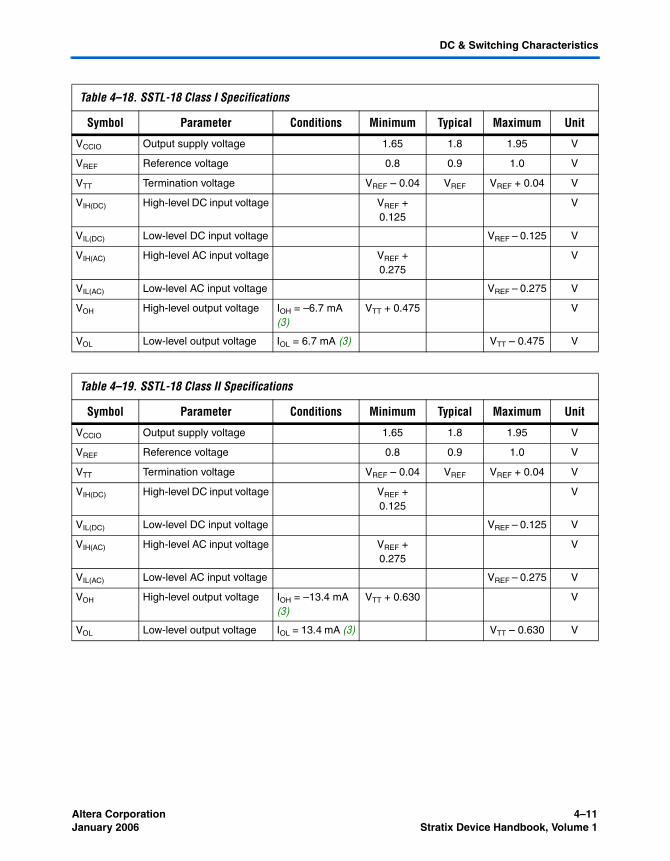
Altera Corporation 4–11January 2006 Stratix Device Handbook, Volume 1
DC & Switching Characteristics
Table 4–18. SSTL-18 Class I Specifications
Symbol Parameter Conditions Minimum Typical Maximum Unit
VCCIO Output supply voltage 1.65 1.8 1.95 V
VREF Reference voltage 0.8 0.9 1.0 V
VTT Termination voltage VREF – 0.04 VREF VREF + 0.04 V
VIH(DC) High-level DC input voltage VREF + 0.125
V
VIL(DC) Low-level DC input voltage VREF – 0.125 V
VIH(AC) High-level AC input voltage VREF + 0.275
V
VIL(AC) Low-level AC input voltage VREF – 0.275 V
VOH High-level output voltage IOH = –6.7 mA (3)
VTT + 0.475 V
VOL Low-level output voltage IOL = 6.7 mA (3) VTT – 0.475 V
Table 4–19. SSTL-18 Class II Specifications
Symbol Parameter Conditions Minimum Typical Maximum Unit
VCCIO Output supply voltage 1.65 1.8 1.95 V
VREF Reference voltage 0.8 0.9 1.0 V
VTT Termination voltage VREF – 0.04 VREF VREF + 0.04 V
VIH(DC) High-level DC input voltage VREF + 0.125
V
VIL(DC) Low-level DC input voltage VREF – 0.125 V
VIH(AC) High-level AC input voltage VREF + 0.275
V
VIL(AC) Low-level AC input voltage VREF – 0.275 V
VOH High-level output voltage IOH = –13.4 mA (3)
VTT + 0.630 V
VOL Low-level output voltage IOL = 13.4 mA (3) VTT – 0.630 V
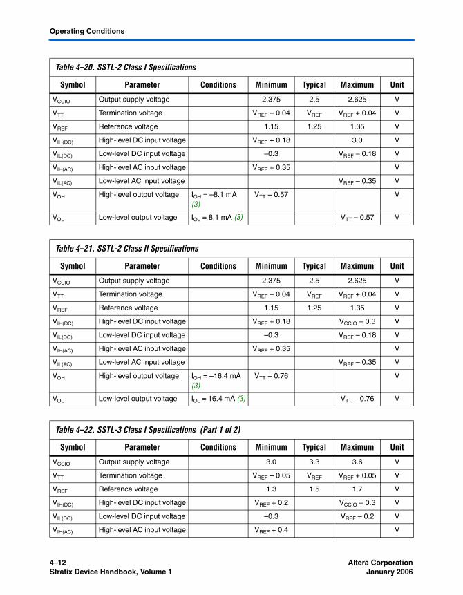
4–12 Altera CorporationStratix Device Handbook, Volume 1 January 2006
Operating Conditions
Table 4–20. SSTL-2 Class I Specifications
Symbol Parameter Conditions Minimum Typical Maximum Unit
VCCIO Output supply voltage 2.375 2.5 2.625 V
VTT Termination voltage VREF – 0.04 VREF VREF + 0.04 V
VREF Reference voltage 1.15 1.25 1.35 V
VIH(DC) High-level DC input voltage VREF + 0.18 3.0 V
VIL(DC) Low-level DC input voltage –0.3 VREF – 0.18 V
VIH(AC) High-level AC input voltage VREF + 0.35 V
VIL(AC) Low-level AC input voltage VREF – 0.35 V
VOH High-level output voltage IOH = –8.1 mA (3)
VTT + 0.57 V
VOL Low-level output voltage IOL = 8.1 mA (3) VTT – 0.57 V
Table 4–21. SSTL-2 Class II Specifications
Symbol Parameter Conditions Minimum Typical Maximum Unit
VCCIO Output supply voltage 2.375 2.5 2.625 V
VTT Termination voltage VREF – 0.04 VREF VREF + 0.04 V
VREF Reference voltage 1.15 1.25 1.35 V
VIH(DC) High-level DC input voltage VREF + 0.18 VCCIO + 0.3 V
VIL(DC) Low-level DC input voltage –0.3 VREF – 0.18 V
VIH(AC) High-level AC input voltage VREF + 0.35 V
VIL(AC) Low-level AC input voltage VREF – 0.35 V
VOH High-level output voltage IOH = –16.4 mA (3)
VTT + 0.76 V
VOL Low-level output voltage IOL = 16.4 mA (3) VTT – 0.76 V
Table 4–22. SSTL-3 Class I Specifications (Part 1 of 2)
Symbol Parameter Conditions Minimum Typical Maximum Unit
VCCIO Output supply voltage 3.0 3.3 3.6 V
VTT Termination voltage VREF – 0.05 VREF VREF + 0.05 V
VREF Reference voltage 1.3 1.5 1.7 V
VIH(DC) High-level DC input voltage VREF + 0.2 VCCIO + 0.3 V
VIL(DC) Low-level DC input voltage –0.3 VREF – 0.2 V
VIH(AC) High-level AC input voltage VREF + 0.4 V

Altera Corporation 4–13January 2006 Stratix Device Handbook, Volume 1
DC & Switching Characteristics
VIL(AC) Low-level AC input voltage VREF – 0.4 V
VOH High-level output voltage IOH = –8 mA (3) VTT + 0.6 V
VOL Low-level output voltage IOL = 8 mA (3) VTT – 0.6 V
Table 4–23. SSTL-3 Class II Specifications
Symbol Parameter Conditions Minimum Typical Maximum Unit
VCCIO Output supply voltage 3.0 3.3 3.6 V
VTT Termination voltage VREF – 0.05 VREF VREF + 0.05 V
VREF Reference voltage 1.3 1.5 1.7 V
VIH(DC) High-level DC input voltage VREF + 0.2 VCCIO + 0.3 V
VIL(DC) Low-level DC input voltage –0.3 VREF – 0.2 V
VIH(AC) High-level AC input voltage VREF + 0.4 V
VIL(AC) Low-level AC input voltage VREF – 0.4 V
VOH High-level output voltage IOH = –16 mA (3) VT T + 0.8 V
VOL Low-level output voltage IOL = 16 mA (3) VTT – 0.8 V
Table 4–24. 3.3-V AGP 2× Specifications
Symbol Parameter Conditions Minimum Typical Maximum Unit
VCCIO Output supply voltage 3.15 3.3 3.45 V
VREF Reference voltage 0.39 × VCCIO 0.41 × VCCIO V
VIH High-level input voltage (4) 0.5 × VCCIO VCCIO + 0.5 V
VIL Low-level input voltage (4) 0.3 × VCCIO V
VOH High-level output voltage IOUT = –0.5 mA 0.9 × VCCIO 3.6 V
VOL Low-level output voltage IOUT = 1.5 mA 0.1 × VCCIO V
Table 4–25. 3.3-V AGP 1× Specifications (Part 1 of 2)
Symbol Parameter Conditions Minimum Typical Maximum Unit
VCCIO Output supply voltage 3.15 3.3 3.45 V
VIH High-level input voltage (4) 0.5 × VCCIO VCCIO + 0.5 V
VIL Low-level input voltage (4) 0.3 × VCCIO V
Table 4–22. SSTL-3 Class I Specifications (Part 2 of 2)
Symbol Parameter Conditions Minimum Typical Maximum Unit

4–14 Altera CorporationStratix Device Handbook, Volume 1 January 2006
Operating Conditions
VOH High-level output voltage IOUT = –0.5 mA 0.9 × VCCIO 3.6 V
VOL Low-level output voltage IOUT = 1.5 mA 0.1 × VCCIO V
Table 4–26. 1.5-V HSTL Class I Specifications
Symbol Parameter Conditions Minimum Typical Maximum Unit
VCCIO Output supply voltage 1.4 1.5 1.6 V
VREF Input reference voltage 0.68 0.75 0.9 V
VTT Termination voltage 0.7 0.75 0.8 V
VIH (DC) DC high-level input voltage VREF + 0.1 V
VIL (DC) DC low-level input voltage –0.3 VREF – 0.1 V
VIH (AC) AC high-level input voltage VREF + 0.2 V
VIL (AC) AC low-level input voltage VREF – 0.2 V
VOH High-level output voltage IOH = –8 mA (3) VCCIO – 0.4 V
VOL Low-level output voltage IOL = 8 mA (3) 0.4 V
Table 4–27. 1.5-V HSTL Class II Specifications
Symbol Parameter Conditions Minimum Typical Maximum Unit
VCCIO Output supply voltage 1.4 1.5 1.6 V
VREF Input reference voltage 0.68 0.75 0.9 V
VTT Termination voltage 0.7 0.75 0.8 V
VIH (DC) DC high-level input voltage VREF + 0.1 V
VIL (DC) DC low-level input voltage –0.3 VREF – 0.1 V
VIH (AC) AC high-level input voltage VREF + 0.2 V
VIL (AC) AC low-level input voltage VREF – 0.2 V
VOH High-level output voltage IOH = –16 mA (3) VCCIO – 0.4 V
VOL Low-level output voltage IOL = 16 mA (3) 0.4 V
Table 4–25. 3.3-V AGP 1× Specifications (Part 2 of 2)
Symbol Parameter Conditions Minimum Typical Maximum Unit

Altera Corporation 4–15January 2006 Stratix Device Handbook, Volume 1
DC & Switching Characteristics
Table 4–28. 1.8-V HSTL Class I Specifications
Symbol Parameter Conditions Minimum Typical Maximum Unit
VCCIO Output supply voltage 1.65 1.80 1.95 V
VREF Input reference voltage 0.70 0.90 0.95 V
VTT Termination voltage VCCIO × 0.5
V
VIH (DC) DC high-level input voltage VREF + 0.1 V
VIL (DC) DC low-level input voltage –0.5 VREF – 0.1 V
VIH (AC) AC high-level input voltage VREF + 0.2 V
VIL (AC) AC low-level input voltage VREF – 0.2 V
VOH High-level output voltage IOH = –8 mA (3) VCCIO – 0.4 V
VOL Low-level output voltage IOL = 8 mA (3) 0.4 V
Table 4–29. 1.8-V HSTL Class II Specifications
Symbol Parameter Conditions Minimum Typical Maximum Unit
VCCIO Output supply voltage 1.65 1.80 1.95 V
VREF Input reference voltage 0.70 0.90 0.95 V
VTT Termination voltage VCCIO × 0.5
V
VIH (DC) DC high-level input voltage VREF + 0.1 V
VIL (DC) DC low-level input voltage –0.5 VREF – 0.1 V
VIH (AC) AC high-level input voltage VREF + 0.2 V
VIL (AC) AC low-level input voltage VREF – 0.2 V
VOH High-level output voltage IOH = –16 mA (3) VCCIO – 0.4 V
VOL Low-level output voltage IOL = 16 mA (3) 0.4 V
Table 4–30. 1.5-V Differential HSTL Class I & Class II Specifications
Symbol Parameter Conditions Minimum Typical Maximum Unit
VCCIO I/O supply voltage 1.4 1.5 1.6 V
VDIF (DC) DC input differential voltage
0.2 V
VCM (DC) DC common mode input voltage
0.68 0.9 V
VDIF (AC) AC differential input voltage
0.4 V

4–16 Altera CorporationStratix Device Handbook, Volume 1 January 2006
Operating Conditions
Table 4–31. CTT I/O Specifications
Symbol Parameter Conditions Minimum Typical Maximum Unit
VCCIO Output supply voltage 2.05 3.3 3.6 V
VTT/VREF Termination and input reference voltage
1.35 1.5 1.65 V
VIH High-level input voltage VREF + 0.2 V
VIL Low-level input voltage VREF – 0.2 V
VOH High-level output voltage IOH = –8 mA VREF + 0.4 V
VOL Low-level output voltage IOL = 8 mA VREF – 0.4 V
IO Output leakage current (when output is high Z)
GND ≤ VOUT ≤ VCCIO
–10 10 μA
Table 4–32. Bus Hold Parameters
Parameter Conditions
VCCIO Level
Unit1.5 V 1.8 V 2.5 V 3.3 V
Min Max Min Max Min Max Min Max
Low sustaining current
VIN > VIL (maximum)
25 30 50 70 μA
High sustaining current
VIN < VIH (minimum)
-25 –30 –50 –70 μA
Low overdrive current
0 V < VIN < VCCIO
160 200 300 500 μA
High overdrive current
0 V < VIN < VCCIO
-160 –200 –300 –500 μA
Bus-hold trip point
0.5 1.0 0.68 1.07 0.7 1.7 0.8 2.0 V

Altera Corporation 4–17January 2006 Stratix Device Handbook, Volume 1
DC & Switching Characteristics
Power Consumption
Altera® offers two ways to calculate power for a design: the Altera web power calculator and the PowerGaugeTM feature in the Quartus® II software.
The interactive power calculator on the Altera web site is typically used prior to designing the FPGA in order to get a magnitude estimate of the device power. The Quartus II software PowerGauge feature allows you to apply test vectors against your design for more accurate power consumption modeling.
In both cases, these calculations should only be used as an estimation of power, not as a specification.
Stratix devices require a certain amount of power-up current to successfully power up because of the small process geometry on which they are fabricated.
Table 4–34 shows the maximum power-up current (ICCINT) required to power a Stratix device. This specification is for commercial operating conditions. Measurements were performed with an isolated Stratix device on the board to characterize the power-up current of an isolated
Table 4–33. Stratix Device Capacitance Note (5)
Symbol Parameter Minimum Typical Maximum Unit
CIOTB Input capacitance on I/O pins in I/O banks 3, 4, 7, and 8.
11.5 pF
CIOLR Input capacitance on I/O pins in I/O banks 1, 2, 5, and 6, including high-speed differential receiver and transmitter pins.
8.2 pF
CCLKTB Input capacitance on top/bottom clock input pins: CLK[4:7] and CLK[12:15].
11.5 pF
CCLKLR Input capacitance on left/right clock inputs: CLK1, CLK3, CLK8, CLK10.
7.8 pF
CCLKLR+ Input capacitance on left/right clock inputs: CLK0, CLK2, CLK9, and CLK11.
4.4 pF
Notes to Tables 4–10 through 4–33:(1) When tx_outclock port of altlvds_tx megafunction is 717 MHz, VO D ( m i n ) = 235 mV on the output clock pin.(2) Pin pull-up resistance values will lower if an external source drives the pin higher than VCCIO.(3) Drive strength is programmable according to the values shown in the Stratix Architecture chapter of the Stratix
Device Handbook, Volume 1.(4) VREF specifies the center point of the switching range.(5) Capacitance is sample-tested only. Capacitance is measured using time-domain reflections (TDR). Measurement
accuracy is within ±0.5 pF.(6) VIO and VCM have multiple ranges and values for J=1 through 10.
4–18 Altera CorporationStratix Device Handbook, Volume 1 January 2006
Power Consumption
device. Decoupling capacitors were not used in this measurement. To factor in the current for decoupling capacitors, sum up the current for each capacitor using the following equation:
I = C (dV/dt)
If the regulator or power supply minimum output current is more than the Stratix device requires, then the device may consume more current than the maximum current listed in Table 4–34. However, the device does not require any more current to successfully power up than what is listed in Table 4–34.
The exact amount of current consumed varies according to the process, temperature, and power ramp rate. Stratix devices typically require less current during power up than shown in Table 4–34. The user-mode current during device operation is generally higher than the power-up current.
The duration of the ICCINT power-up requirement depends on the VCCINT voltage supply rise time. The power-up current consumption drops when the VCCINT supply reaches approximately 0.75 V.
Table 4–34. Stratix Power-Up Current (ICCINT) Requirements Note (1)
DevicePower-Up Current Requirement
UnitTypical Maximum
EP1S10 250 700 mA
EP1S20 400 1,200 mA
EP1S25 500 1,500 mA
EP1S30 550 1,900 mA
EP1S40 650 2,300 mA
EP1S60 800 2,600 mA
EP1S80 1,000 3,000 mA
Note to Table 4–34:
(1) The maximum test conditions are for 0° C and typical test conditions are for 40° C.
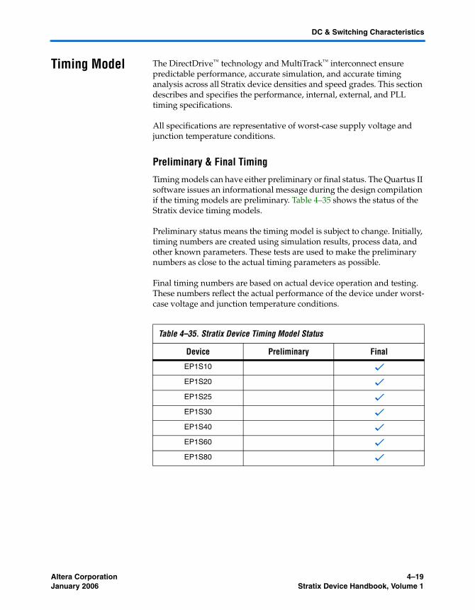
Altera Corporation 4–19January 2006 Stratix Device Handbook, Volume 1
DC & Switching Characteristics
Timing Model The DirectDrive™ technology and MultiTrack™ interconnect ensure predictable performance, accurate simulation, and accurate timing analysis across all Stratix device densities and speed grades. This section describes and specifies the performance, internal, external, and PLL timing specifications.
All specifications are representative of worst-case supply voltage and junction temperature conditions.
Preliminary & Final Timing
Timing models can have either preliminary or final status. The Quartus II software issues an informational message during the design compilation if the timing models are preliminary. Table 4–35 shows the status of the Stratix device timing models.
Preliminary status means the timing model is subject to change. Initially, timing numbers are created using simulation results, process data, and other known parameters. These tests are used to make the preliminary numbers as close to the actual timing parameters as possible.
Final timing numbers are based on actual device operation and testing. These numbers reflect the actual performance of the device under worst-case voltage and junction temperature conditions.
Table 4–35. Stratix Device Timing Model Status
Device Preliminary Final
EP1S10 v
EP1S20 v
EP1S25 v
EP1S30 v
EP1S40 v
EP1S60 v
EP1S80 v
4–20 Altera CorporationStratix Device Handbook, Volume 1 January 2006
Timing Model
Performance
Table 4–36 shows Stratix performance for some common designs. All performance values were obtained with Quartus II software compilation of LPM, or MegaCore® functions for the FIR and FFT designs.
Table 4–36. Stratix Performance (Part 1 of 2) Notes (1), (2)
Applications
Resources Used Performance
LEsTriMatrix Memory Blocks
DSP Blocks
-5 Speed Grade
-6 Speed Grade
-7 Speed Grade
-8 Speed Grade
Units
LE 16-to-1 multiplexer (1) 22 0 0 407.83 324.56 288.68 228.67 MHz
32-to-1 multiplexer (3) 46 0 0 318.26 255.29 242.89 185.18 MHz
16-bit counter 16 0 0 422.11 422.11 390.01 348.67 MHz
64-bit counter 64 0 0 321.85 290.52 261.23 220.5 MHz
TriMatrix memory M512 block
Simple dual-port RAM 32 × 18 bit
0 1 0 317.76 277.62 241.48 205.21 MHz
FIFO 32 × 18 bit 30 1 0 319.18 278.86 242.54 206.14 MHz
TriMatrix memory M4K block
Simple dual-port RAM 128 × 36 bit
0 1 0 290.86 255.55 222.27 188.89 MHz
True dual-port RAM 128 × 18 bit
0 1 0 290.86 255.55 222.27 188.89 MHz
FIFO 128 × 36 bit 34 1 0 290.86 255.55 222.27 188.89 MHz
TriMatrix memory M-RAM block
Single portRAM 4K × 144 bit
1 1 0 255.95 223.06 194.06 164.93 MHz
Simple dual-portRAM 4K × 144 bit
0 1 0 255.95 233.06 194.06 164.93 MHz
True dual-portRAM 4K × 144 bit
0 1 0 255.95 233.06 194.06 164.93 MHz
Single portRAM 8K × 72 bit
0 1 0 278.94 243.19 211.59 179.82 MHz
Simple dual-portRAM 8K × 72 bit
0 1 0 255.95 223.06 194.06 164.93 MHz
True dual-portRAM 8K × 72 bit
0 1 0 255.95 223.06 194.06 164.93 MHz
Single portRAM 16K × 36 bit
0 1 0 280.66 254.32 221.28 188.00 MHz
Simple dual-portRAM 16K × 36 bit
0 1 0 269.83 237.69 206.82 175.74 MHz

Altera Corporation 4–21January 2006 Stratix Device Handbook, Volume 1
DC & Switching Characteristics
TriMatrix memory M-RAM block
True dual-portRAM 16K × 36 bit
0 1 0 269.83 237.69 206.82 175.74 MHz
Single portRAM 32K × 18 bit
0 1 0 275.86 244.55 212.76 180.83 MHz
Simple dual-portRAM 32K × 18 bit
0 1 0 275.86 244.55 212.76 180.83 MHz
True dual-portRAM 32K × 18 bit
0 1 0 275.86 244.55 212.76 180.83 MHz
Single portRAM 64K × 9 bit
0 1 0 287.85 253.29 220.36 187.26 MHz
Simple dual-portRAM 64K × 9 bit
0 1 0 287.85 253.29 220.36 187.26 MHz
True dual-portRAM 64K × 9 bit
0 1 0 287.85 253.29 220.36 187.26 MHz
DSP block 9 × 9-bit multiplier (3) 0 0 1 335.0 293.94 255.68 217.24 MHz
18 × 18-bit multiplier (4)
0 0 1 278.78 237.41 206.52 175.50 MHz
36 × 36-bit multiplier (4)
0 0 1 148.25 134.71 117.16 99.59 MHz
36 × 36-bit multiplier (5)
0 0 1 278.78 237.41 206.52 175.5 MHz
18-bit, 4-tap FIR filter 0 0 1 278.78 237.41 206.52 175.50 MHz
Larger Designs
8-bit, 16-tap parallel FIR filter
58 0 4 141.26 133.49 114.88 100.28 MHz
8-bit, 1,024-point FFT function
870 5 1 261.09 235.51 205.21 175.22 MHz
Notes to Table 4–36:(1) These design performance numbers were obtained using the Quartus II software.(2) Numbers not listed will be included in a future version of the data sheet.(3) This application uses registered inputs and outputs.(4) This application uses registered multiplier input and output stages within the DSP block.(5) This application uses registered multiplier input, pipeline, and output stages within the DSP
block.
Table 4–36. Stratix Performance (Part 2 of 2) Notes (1), (2)
Applications
Resources Used Performance
LEsTriMatrix Memory Blocks
DSP Blocks
-5 Speed Grade
-6 Speed Grade
-7 Speed Grade
-8 Speed Grade
Units

4–22 Altera CorporationStratix Device Handbook, Volume 1 January 2006
Timing Model
Internal Timing Parameters
Internal timing parameters are specified on a speed grade basis independent of device density. Tables 4–37 through 4–42 describe the Stratix device internal timing microparameters for LEs, IOEs, TriMatrix™ memory structures, DSP blocks, and MultiTrack interconnects.
Table 4–37. LE Internal Timing Microparameter Descriptions
Symbol Parameter
tSU LE register setup time before clock
tH LE register hold time after clock
tCO LE register clock-to-output delay
tLUT LE combinatorial LUT delay for data-in to data-out
tCLR Minimum clear pulse width
tPRE Minimum preset pulse width
tCLKHL Register minimum clock high or low time. The maximum core clock frequency can be calculated by 1/(2 × tCLKHL).
Table 4–38. IOE Internal Timing Microparameter Descriptions
Symbol Parameter
tSU_R Row IOE input register setup time
tSU_C Column IOE input register setup time
tH IOE input and output register hold time after clock
tCO_R Row IOE input and output register clock-to-output delay
tC O _ C Column IOE input and output register clock-to-output delay
tPIN2COMBOUT_R Row input pin to IOE combinatorial output
tPIN2COMBOUT_C Column input pin to IOE combinatorial output
tCOMBIN2PIN_R Row IOE data input to combinatorial output pin
tCOMBIN2PIN_C Column IOE data input to combinatorial output pin
tCLR Minimum clear pulse width
tPRE Minimum preset pulse width
tCLKHL Register minimum clock high or low time. The maximum I/O clock frequency can be calculated by 1/(2 × tCLKHL). Performance may also be affected by I/O timing, use of PLL, and I/O programmable settings.

Altera Corporation 4–23January 2006 Stratix Device Handbook, Volume 1
DC & Switching Characteristics
Table 4–39. DSP Block Internal Timing Microparameter Descriptions
Symbol Parameter
tSU Input, pipeline, and output register setup time before clock
tH Input, pipeline, and output register hold time after clock
tCO Input, pipeline, and output register clock-to-output delay
tINREG2PIPE9 Input Register to DSP Block pipeline register in 9 × 9-bit mode
tINREG2PIPE18 Input Register to DSP Block pipeline register in 18 × 18-bit mode
tPIPE2OUTREG2ADD DSP Block Pipeline Register to output register delay in Two-Multipliers Adder mode
tPIPE2OUTREG4ADD DSP Block Pipeline Register to output register delay in Four-Multipliers Adder mode
tPD9 Combinatorial input to output delay for 9 × 9
tPD18 Combinatorial input to output delay for 18 × 18
tPD36 Combinatorial input to output delay for 36 × 36
tCLR Minimum clear pulse width
tCLKHL Register minimum clock high or low time. This is a limit on the min time for the clock on the registers in these blocks. The actual performance is dependent upon the internal point-to-point delays in the blocks and may give slower performance as shown in Table 4–36 on page 4–20 and as reported by the timing analyzer in the Quartus II software.

4–24 Altera CorporationStratix Device Handbook, Volume 1 January 2006
Timing Model
Table 4–40. M512 Block Internal Timing Microparameter Descriptions
Symbol Parameter
tM512RC Synchronous read cycle time
tM512WC Synchronous write cycle time
tM512WERESU Write or read enable setup time before clock
tM512WEREH Write or read enable hold time after clock
tM512CLKENSU Clock enable setup time before clock
tM512CLKENH Clock enable hold time after clock
tM512DATASU Data setup time before clock
tM512DATAH Data hold time after clock
tM512WADDRSU Write address setup time before clock
tM512WADDRH Write address hold time after clock
tM512RADDRSU Read address setup time before clock
tM512RADDRH Read address hold time after clock
tM512DATACO1 Clock-to-output delay when using output registers
tM512DATACO2 Clock-to-output delay without output registers
tM512CLKHL Register minimum clock high or low time. This is a limit on the min time for the clock on the registers in these blocks. The actual performance is dependent upon the internal point-to-point delays in the blocks and may give slower performance as shown in Table 4–36 on page 4–20 and as reported by the timing analyzer in the Quartus II software.
tM512CLR Minimum clear pulse width
Table 4–41. M4K Block Internal Timing Microparameter Descriptions (Part 1 of 2)
Symbol Parameter
tM4KRC Synchronous read cycle time
tM4KWC Synchronous write cycle time
tM4KWERESU Write or read enable setup time before clock
tM4KWEREH Write or read enable hold time after clock
tM4KCLKENSU Clock enable setup time before clock
tM4KCLKENH Clock enable hold time after clock
tM4KBESU Byte enable setup time before clock
tM4KBEH Byte enable hold time after clock
tM4KDATAASU A port data setup time before clock

Altera Corporation 4–25January 2006 Stratix Device Handbook, Volume 1
DC & Switching Characteristics
tM4KDATAAH A port data hold time after clock
tM4KADDRASU A port address setup time before clock
tM4KADDRAH A port address hold time after clock
tM4KDATABSU B port data setup time before clock
tM4KDATABH B port data hold time after clock
tM4KADDRBSU B port address setup time before clock
tM4KADDRBH B port address hold time after clock
tM4KDATACO1 Clock-to-output delay when using output registers
tM4KDATACO2 Clock-to-output delay without output registers
tM4KCLKHL Register minimum clock high or low time. This is a limit on the min time for the clock on the registers in these blocks. The actual performance is dependent upon the internal point-to-point delays in the blocks and may give slower performance as shown inTable 4–36 on page 4–20 and as reported by the timing analyzer in the Quartus II software.
tM4KCLR Minimum clear pulse width
Table 4–42. M-RAM Block Internal Timing Microparameter Descriptions (Part 1 of 2)
Symbol Parameter
tMRAMRC Synchronous read cycle time
tMRAMWC Synchronous write cycle time
tMRAMWERESU Write or read enable setup time before clock
tMRAMWEREH Write or read enable hold time after clock
tMRAMCLKENSU Clock enable setup time before clock
tMRAMCLKENH Clock enable hold time after clock
tMRAMBESU Byte enable setup time before clock
tMRAMBEH Byte enable hold time after clock
tMRAMDATAASU A port data setup time before clock
tMRAMDATAAH A port data hold time after clock
tMRAMADDRASU A port address setup time before clock
tMRAMADDRAH A port address hold time after clock
tMRAMDATABSU B port setup time before clock
Table 4–41. M4K Block Internal Timing Microparameter Descriptions (Part 2 of 2)
Symbol Parameter

4–26 Altera CorporationStratix Device Handbook, Volume 1 January 2006
Timing Model
tMRAMDATABH B port hold time after clock
tMRAMADDRBSU B port address setup time before clock
tMRAMADDRBH B port address hold time after clock
tMRAMDATACO1 Clock-to-output delay when using output registers
tMRAMDATACO2 Clock-to-output delay without output registers
tMRAMCLKHL Register minimum clock high or low time. This is a limit on the min time for the clock on the registers in these blocks. The actual performance is dependent upon the internal point-to-point delays in the blocks and may give slower performance as shown in Table 4–36 on page 4–20 and as reported by the timing analyzer in the Quartus II software.
tMRAMCLR Minimum clear pulse width.
Table 4–42. M-RAM Block Internal Timing Microparameter Descriptions (Part 2 of 2)
Symbol Parameter
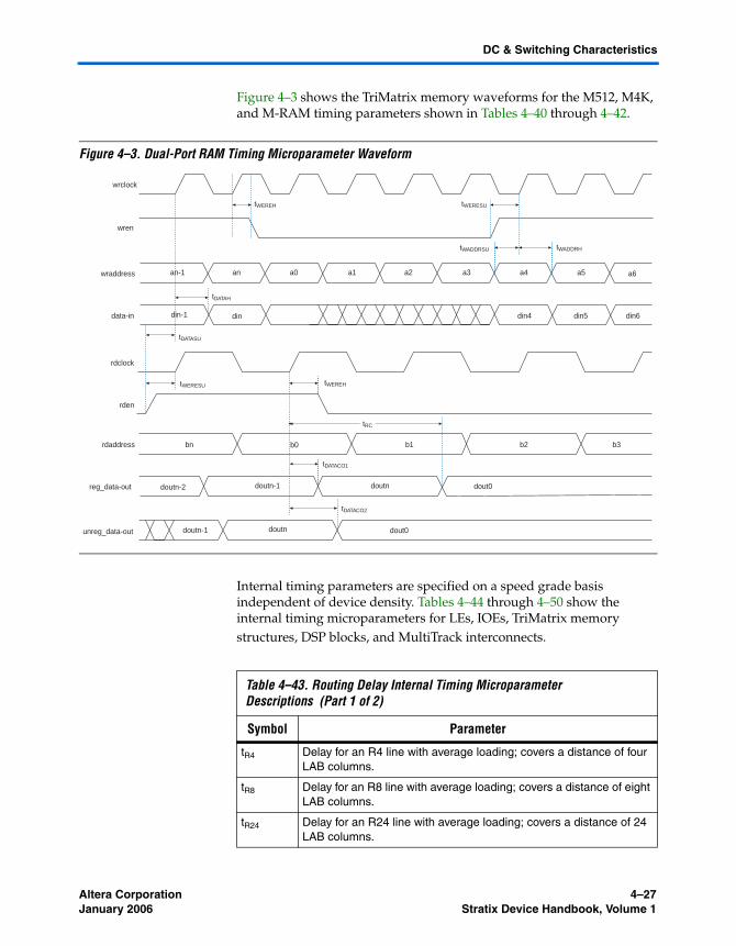
Altera Corporation 4–27January 2006 Stratix Device Handbook, Volume 1
DC & Switching Characteristics
Figure 4–3 shows the TriMatrix memory waveforms for the M512, M4K, and M-RAM timing parameters shown in Tables 4–40 through 4–42.
Figure 4–3. Dual-Port RAM Timing Microparameter Waveform
Internal timing parameters are specified on a speed grade basis independent of device density. Tables 4–44 through 4–50 show the internal timing microparameters for LEs, IOEs, TriMatrix memory structures, DSP blocks, and MultiTrack interconnects.
wrclock
wren
wraddress
data-in
reg_data-out
an-1 an a0 a1 a2 a3 a4 a5
din-1 din din4 din5
rdclock
a6
din6
unreg_data-out
rden
rdaddress bn b0 b1 b2 b3
doutn-2 doutn-1 doutn
doutn-1 doutn dout0
tWERESU tWEREH
tDATACO1
tDATACO2
tDATASU
tDATAH
tWEREH tWERESU
tWADDRSU tWADDRH
dout0
tRC
Table 4–43. Routing Delay Internal Timing Microparameter Descriptions (Part 1 of 2)
Symbol Parameter
tR4 Delay for an R4 line with average loading; covers a distance of four LAB columns.
tR8 Delay for an R8 line with average loading; covers a distance of eight LAB columns.
tR24 Delay for an R24 line with average loading; covers a distance of 24 LAB columns.

4–28 Altera CorporationStratix Device Handbook, Volume 1 January 2006
Timing Model
tC4 Delay for a C4 line with average loading; covers a distance of four LAB rows.
tC8 Delay for a C8 line with average loading; covers a distance of eight LAB rows.
tC16 Delay for a C16 line with average loading; covers a distance of 16 LAB rows.
tLOCAL Local interconnect delay, for connections within a LAB, and for the final routing hop of connections to LABs, DSP blocks, RAM blocks and I/Os.
Table 4–43. Routing Delay Internal Timing Microparameter Descriptions (Part 2 of 2)
Symbol Parameter
Table 4–44. LE Internal Timing Microparameters
Parameter-5 -6 -7 -8
UnitMin Max Min Max Min Max Min Max
tSU 10 10 11 13 ps
tH 100 100 114 135 ps
tCO 156 176 202 238 ps
tLUT 366 459 527 621 ps
tCLR 100 100 114 135 ps
tPRE 100 100 114 135 ps
tCLKHL 1000 1111 1190 1400 ps
Table 4–45. IOE Internal TSU Microparameter by Device Density (Part 1 of 2)
Device Symbol-5 -6 -7 -8 Unit
Min Max Min Max Min Max Min Max
EP1S10 tSU_R 76 80 80 80 ps
tSU_C 176 80 80 80 ps
EP1S20 tSU_R 76 80 80 80 ps
tSU_C 76 80 80 80 ps
EP1S25 tSU_R 276 280 280 280 ps
tSU_C 276 280 280 280 ps
EP1S30 tSU_R 76 80 80 80 ps
tSU_C 176 180 180 180 ps
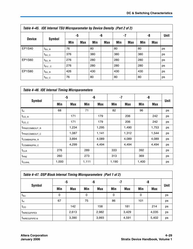
Altera Corporation 4–29January 2006 Stratix Device Handbook, Volume 1
DC & Switching Characteristics
EP1S40 tSU_R 76 80 80 80 ps
tSU_C 376 380 380 380 ps
EP1S60 tSU_R 276 280 280 280 ps
tS U_ C 276 280 280 280 ps
EP1S80 tSU_R 426 430 430 430 ps
tSU_C 76 80 80 80 ps
Table 4–46. IOE Internal Timing Microparameters
Symbol-5 -6 -7 -8
UnitMin Max Min Max Min Max Min Max
tH 68 71 82 96 ps
tCO_R 171 179 206 242 ps
tCO_C 171 179 206 242 ps
tPIN2COMBOUT_R 1,234 1,295 1,490 1,753 ps
tPIN2COMBOUT_C 1,087 1,141 1,312 1,544 ps
tCOMBIN2PIN_R 3,894 4,089 4,089 4,089 ps
tCOMBIN2PIN_C 4,299 4,494 4,494 4,494 ps
tCLR 276 289 333 392 ps
tPRE 260 273 313 369 ps
tCLKHL 1,000 1,111 1,190 1,400 ps
Table 4–47. DSP Block Internal Timing Microparameters (Part 1 of 2)
Symbol-5 -6 -7 -8
UnitMin Max Min Max Min Max Min Max
tSU 0 0 0 0 ps
tH 67 75 86 101 ps
tCO 142 158 181 214 ps
tINREG2PIPE9 2,613 2,982 3,429 4,035 ps
tINREG2PIPE18 3,390 3,993 4,591 5,402 ps
Table 4–45. IOE Internal TSU Microparameter by Device Density (Part 2 of 2)
Device Symbol-5 -6 -7 -8 Unit
Min Max Min Max Min Max Min Max

4–30 Altera CorporationStratix Device Handbook, Volume 1 January 2006
Timing Model
tPIPE2OUTREG2ADD 2,002 2,203 2,533 2,980 ps
tPIPE2OUTREG4ADD 2,899 3,189 3,667 4,314 ps
tPD9 3,709 4,081 4,692 5,520 ps
tPD18 4,795 5,275 6,065 7,135 ps
tPD36 7,495 8,245 9,481 11,154 ps
tCLR 450 500 575 676 ps
tCLKHL 1,350 1,500 1,724 2,029 ps
Table 4–48. M512 Block Internal Timing Microparameters
Symbol-5 -6 -7 -8
UnitMin Max Min Max Min Max Min Max
tM512RC 3,340 3,816 4,387 5,162 ps
tM512WC 3,138 3,590 4,128 4,860 ps
tM512WERESU 110 123 141 166 ps
tM512WEREH 34 38 43 51 ps
tM512CLKENSU 215 215 247 290 ps
tM512CLKENH –70 –70 –81 –95 ps
tM512DATASU 110 123 141 166 ps
tM512DATAH 34 38 43 51 ps
tM512WADDRSU 110 123 141 166 ps
tM512WADDRH 34 38 43 51 ps
tM512RADDRSU 110 123 141 166 ps
tM512RADDRH 34 38 43 51 ps
tM512DATACO1 424 472 541 637 ps
tM512DATACO2 3,366 3,846 4,421 5,203 ps
tM512CLKHL 1,000 1,111 1,190 1,400 ps
tM512CLR 170 189 217 255 ps
Table 4–47. DSP Block Internal Timing Microparameters (Part 2 of 2)
Symbol-5 -6 -7 -8
UnitMin Max Min Max Min Max Min Max

Altera Corporation 4–31January 2006 Stratix Device Handbook, Volume 1
DC & Switching Characteristics
Table 4–49. M4K Block Internal Timing Microparameters
Symbol-5 -6 -7 -8
UnitMin Max Min Max Min Max Min Max
tM4KRC 3,807 4,320 4,967 5,844 ps
tM4KWC 2,556 2,840 3,265 3,842 ps
tM4KWERESU 131 149 171 202 ps
tM4KWEREH 34 38 43 51 ps
tM4KCLKENSU 193 215 247 290 ps
tM4KCLKENH –63 –70 –81 –95 ps
tM4KBESU 131 149 171 202 ps
tM4KBEH 34 38 43 51 ps
tM4KDATAASU 131 149 171 202 ps
tM4KDATAAH 34 38 43 51 ps
tM4KADDRASU 131 149 171 202 ps
tM4KADDRAH 34 38 43 51 ps
tM4KDATABSU 131 149 171 202 ps
tM4KDATABH 34 38 43 51 ps
tM4KADDRBSU 131 149 171 202 ps
tM4KADDRBH 34 38 43 51 ps
tM4KDATACO1 571 635 729 858 ps
tM4KDATACO2 3,984 4,507 5,182 6,097 ps
tM4KCLKHL 1,000 1,111 1,190 1,400 ps
tM4KCLR 170 189 217 255 ps
Table 4–50. M-RAM Block Internal Timing Microparameters (Part 1 of 2)
Symbol-5 -6 -7 -8
UnitMin Max Min Max Min Max Min Max
tMRAMRC 4,364 4,838 5,562 6,544 ps
tMRAMWC 3,654 4,127 4,746 5,583 ps
tMRAMWERESU 25 25 28 33 ps
tMRAMWEREH 18 20 23 27 ps
tMRAMCLKENSU 99 111 127 150 ps
tMRAMCLKENH –48 –53 –61 –72 ps
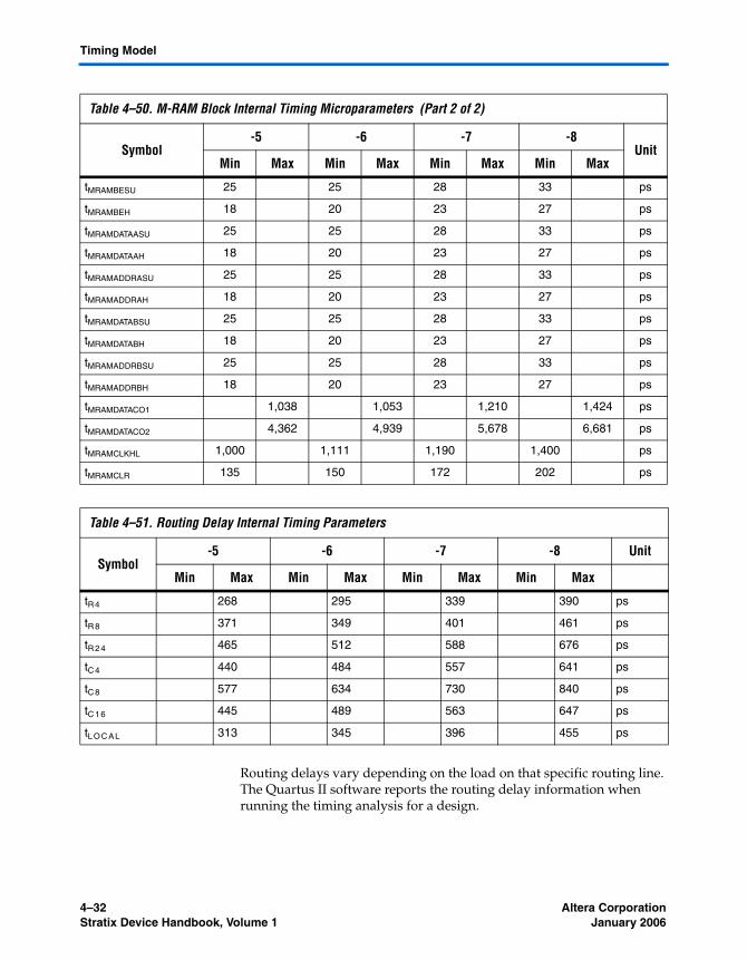
4–32 Altera CorporationStratix Device Handbook, Volume 1 January 2006
Timing Model
Routing delays vary depending on the load on that specific routing line. The Quartus II software reports the routing delay information when running the timing analysis for a design.
tMRAMBESU 25 25 28 33 ps
tMRAMBEH 18 20 23 27 ps
tMRAMDATAASU 25 25 28 33 ps
tMRAMDATAAH 18 20 23 27 ps
tMRAMADDRASU 25 25 28 33 ps
tMRAMADDRAH 18 20 23 27 ps
tMRAMDATABSU 25 25 28 33 ps
tMRAMDATABH 18 20 23 27 ps
tMRAMADDRBSU 25 25 28 33 ps
tMRAMADDRBH 18 20 23 27 ps
tMRAMDATACO1 1,038 1,053 1,210 1,424 ps
tMRAMDATACO2 4,362 4,939 5,678 6,681 ps
tMRAMCLKHL 1,000 1,111 1,190 1,400 ps
tMRAMCLR 135 150 172 202 ps
Table 4–51. Routing Delay Internal Timing Parameters
Symbol-5 -6 -7 -8 Unit
Min Max Min Max Min Max Min Max
tR 4 268 295 339 390 ps
tR 8 371 349 401 461 ps
tR 2 4 465 512 588 676 ps
tC 4 440 484 557 641 ps
tC 8 577 634 730 840 ps
tC 1 6 445 489 563 647 ps
tL O C A L 313 345 396 455 ps
Table 4–50. M-RAM Block Internal Timing Microparameters (Part 2 of 2)
Symbol-5 -6 -7 -8
UnitMin Max Min Max Min Max Min Max

Altera Corporation 4–33January 2006 Stratix Device Handbook, Volume 1
DC & Switching Characteristics
External Timing Parameters
External timing parameters are specified by device density and speed grade. Figure 4–4 shows the pin-to-pin timing model for bidirectional IOE pin timing. All registers are within the IOE.
Figure 4–4. External Timing in Stratix Devices
All external timing parameters reported in this section are defined with respect to the dedicated clock pin as the starting point. All external I/O timing parameters shown are for 3.3-V LVTTL I/O standard with the 24-mA current strength and fast slew rate. For external I/O timing using standards other than LVTTL or for different current strengths, use the I/O standard input and output delay adders in Tables 4–103 through 4–108.
PRN
CLRN
D Q
OE Register
PRN
CLRN
D Q
Input Register
PRN
CLRN
D Q
Output Register
BidirectionalPin
DedicatedClock
tINSUtINHtOUTCOtXZtZX

4–34 Altera CorporationStratix Device Handbook, Volume 1 January 2006
Timing Model
Table 4–52 shows the external I/O timing parameters when using fast regional clock networks.
Table 4–53 shows the external I/O timing parameters when using regional clock networks.
Table 4–52. Stratix Fast Regional Clock External I/O Timing Parameters Notes (1), (2)
Symbol Parameter
tINSU Setup time for input or bidirectional pin using IOE input register with fast regional clock fed by FCLK pin
tINH Hold time for input or bidirectional pin using IOE input register with fast regional clock fed by FCLK pin
tOUTCO Clock-to-output delay output or bidirectional pin using IOE output register with fast regional clock fed by FCLK pin
tXZ Synchronous IOE output enable register to output pin disable delay using fast regional clock fed by FCLK pin
tZX Synchronous IOE output enable register to output pin enable delay using fast regional clock fed by FCLK pin
Notes to Table 4–52:(1) These timing parameters are sample-tested only.(2) These timing parameters are for column and row IOE pins. You should use the
Quartus II software to verify the external timing for any pin.
Table 4–53. Stratix Regional Clock External I/O Timing Parameters (Part 1 of 2) Notes (1), (2)
Symbol Parameter
tINSU Setup time for input or bidirectional pin using IOE input register with regional clock fed by CLK pin
tINH Hold time for input or bidirectional pin using IOE input register with regional clock fed by CLK pin
tOUTCO Clock-to-output delay output or bidirectional pin using IOE output register with regional clock fed by CLK pin
tINSUPLL Setup time for input or bidirectional pin using IOE input register with regional clock fed by Enhanced PLL with default phase setting
tINHPLL Hold time for input or bidirectional pin using IOE input register with regional clock fed by Enhanced PLL with default phase setting
tOUTCOPLL Clock-to-output delay output or bidirectional pin using IOE output register with regional clock Enhanced PLL with default phase setting

Altera Corporation 4–35January 2006 Stratix Device Handbook, Volume 1
DC & Switching Characteristics
Table 4–54 shows the external I/O timing parameters when using global clock networks.
tXZPLL Synchronous IOE output enable register to output pin disable delay using regional clock fed by Enhanced PLL with default phase setting
tZXPLL Synchronous IOE output enable register to output pin enable delay using regional clock fed by Enhanced PLL with default phase setting
Notes to Table 4–53:(1) These timing parameters are sample-tested only.(2) These timing parameters are for column and row IOE pins. You should use the
Quartus II software to verify the external timing for any pin.
Table 4–54. Stratix Global Clock External I/O Timing Parameters Notes (1), (2)
Symbol Parameter
tINSU Setup time for input or bidirectional pin using IOE input register with global clock fed by CLK pin
tINH Hold time for input or bidirectional pin using IOE input register with global clock fed by CLK pin
tOUTCO Clock-to-output delay output or bidirectional pin using IOE output register with global clock fed by CLK pin
tINSUPLL Setup time for input or bidirectional pin using IOE input register with global clock fed by Enhanced PLL with default phase setting
tINHPLL Hold time for input or bidirectional pin using IOE input register with global clock fed by Enhanced PLL with default phase setting
tOUTCOPLL Clock-to-output delay output or bidirectional pin using IOE output register with global clock Enhanced PLL with default phase setting
tXZPLL Synchronous IOE output enable register to output pin disable delay using global clock fed by Enhanced PLL with default phase setting
tZXPLL Synchronous IOE output enable register to output pin enable delay using global clock fed by Enhanced PLL with default phase setting
Notes to Table 4–54:(1) These timing parameters are sample-tested only.(2) These timing parameters are for column and row IOE pins. You should use the
Quartus II software to verify the external timing for any pin.
Table 4–53. Stratix Regional Clock External I/O Timing Parameters (Part 2 of 2) Notes (1), (2)
Symbol Parameter
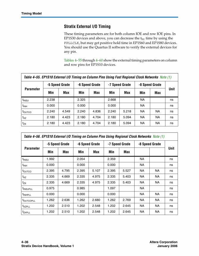
4–36 Altera CorporationStratix Device Handbook, Volume 1 January 2006
Timing Model
Stratix External I/O Timing
These timing parameters are for both column IOE and row IOE pins. In EP1S30 devices and above, you can decrease the tSU time by using the FPLLCLK, but may get positive hold time in EP1S60 and EP1S80 devices. You should use the Quartus II software to verify the external devices for any pin.
Tables 4–55 through 4–60 show the external timing parameters on column and row pins for EP1S10 devices.
Table 4–55. EP1S10 External I/O Timing on Column Pins Using Fast Regional Clock Networks Note (1)
Parameter-5 Speed Grade -6 Speed Grade -7 Speed Grade -8 Speed Grade
UnitMin Max Min Max Min Max Min Max
tINSU 2.238 2.325 2.668 NA ns
tINH 0.000 0.000 0.000 NA ns
tOUTCO 2.240 4.549 2.240 4.836 2.240 5.218 NA NA ns
tXZ 2.180 4.423 2.180 4.704 2.180 5.094 NA NA ns
tZX 2.180 4.423 2.180 4.704 2.180 5.094 NA NA ns
Table 4–56. EP1S10 External I/O Timing on Column Pins Using Regional Clock Networks Note (1)
Parameter-5 Speed Grade -6 Speed Grade -7 Speed Grade -8 Speed Grade
UnitMin Max Min Max Min Max
tINSU 1.992 2.054 2.359 NA ns
tINH 0.000 0.000 0.000 NA ns
tOUTCO 2.395 4.795 2.395 5.107 2.395 5.527 NA NA ns
tXZ 2.335 4.669 2.335 4.975 2.335 5.403 NA NA ns
tZX 2.335 4.669 2.335 4.975 2.335 5.403 NA NA ns
tINSUPLL 0.975 0.985 1.097 NA ns
tINHPLL 0.000 0.000 0.000 NA NA ns
tOUTCOPLL 1.262 2.636 1.262 2.680 1.262 2.769 NA NA ns
tXZPLL 1.202 2.510 1.202 2.548 1.202 2.645 NA NA ns
tZXPLL 1.202 2.510 1.202 2.548 1.202 2.645 NA NA ns

Altera Corporation 4–37January 2006 Stratix Device Handbook, Volume 1
DC & Switching Characteristics
Table 4–57. EP1S10 External I/O Timing on Column Pins Using Global Clock Networks Note (1)
Parameter-5 Speed Grade -6 Speed Grade -7 Speed Grade -8 Speed Grade
UnitMin Max Min Max Min Max Min Max
tINSU 1.647 1.692 1.940 NA ns
tINH 0.000 0.000 0.000 NA ns
tOUTCO 2.619 5.184 2.619 5.515 2.619 5.999 NA NA ns
tXZ 2.559 5.058 2.559 5.383 2.559 5.875 NA NA ns
tZX 2.559 5.058 2.559 5.383 2.559 5.875 NA NA ns
tINSUPLL 1.239 1.229 1.374 NA ns
tINHPLL 0.000 0.000 0.000 NA ns
tOUTCOPLL 1.109 2.372 1.109 2.436 1.109 2.492 NA NA ns
tXZPLL 1.049 2.246 1.049 2.304 1.049 2.368 NA NA ns
tZXPLL 1.049 2.246 1.049 2.304 1.049 2.368 NA NA ns
Table 4–58. EP1S10 External I/O Timing on Row Pin Using Fast Regional Clock Network Note (1)
Parameter-5 Speed Grade -6 Speed Grade -7 Speed Grade -8 Speed Grade
UnitMin Max Min Max Min Max Min Max
tINSU 2.212 2.403 2.759 NA ns
tINH 0.000 0.000 0.000 NA ns
tOUTCO 2.391 4.838 2.391 5.159 2.391 5.569 NA NA ns
tXZ 2.418 4.892 2.418 5.215 2.418 5.637 NA NA ns
tZX 2.418 4.892 2.418 5.215 2.418 5.637 NA NA ns

4–38 Altera CorporationStratix Device Handbook, Volume 1 January 2006
Timing Model
Table 4–59. EP1S10 External I/O Timing on Row Pins Using Regional Clock Networks Note (1)
Parameter-5 Speed Grade -6 Speed Grade -7 Speed Grade -8 Speed Grade
UnitMin Max Min Max Min Max Min Max
tINSU 2.161 2.336 2.685 NA ns
tINH 0.000 0.000 0.000 NA ns
tOUTCO 2.434 4.889 2.434 5.226 2.434 5.643 NA NA ns
tXZ 2.461 4.493 2.461 5.282 2.461 5.711 NA NA ns
tZX 2.461 4.493 2.461 5.282 2.461 5.711 NA NA ns
tINSUPLL 1.057 1.172 1.315 NA ns
tINHPLL 0.000 0.000 0.000 NA ns
tOUTCOPLL 1.327 2.773 1.327 2.848 1.327 2.940 NA NA ns
tXZPLL 1.354 2.827 1.354 2.904 1.354 3.008 NA NA ns
tZXPLL 1.354 2.827 1.354 2.904 1.354 3.008 NA NA ns
Table 4–60. EP1S10 External I/O Timing on Row Pins Using Global Clock Networks Note (1)
Parameter-5 Speed Grade -6 Speed Grade -7 Speed Grade -8 Speed Grade
UnitMin Max Min Max Min Max Min Max
tINSU 1.787 1.944 2.232 NA ns
tINH 0.000 0.000 0.000 NA ns
tOUTCO 2.647 5.263 2.647 5.618 2.647 6.069 NA NA ns
tXZ 2.674 5.317 2.674 5.674 2.674 6.164 NA NA ns
tZX 2.674 5.317 2.674 5.674 2.674 6.164 NA NA ns
tINSUPLL 1.371 1.1472 1.654 NA ns
tINHPLL 0.000 0.000 0.000 NA ns
tOUTCOPLL 1.144 2.459 1.144 2.548 1.144 2.601 NA NA ns
tXZPLL 1.171 2.513 1.171 2.604 1.171 2.669 NA NA ns
tZXPLL 1.171 2.513 1.171 2.604 1.171 2.669 NA NA ns
Note to Tables 4–55 to 4–60:(1) Only EP1S25, EP1S30, and EP1S40 have speed grade of -8.

Altera Corporation 4–39January 2006 Stratix Device Handbook, Volume 1
DC & Switching Characteristics
Tables 4–61 through 4–66 show the external timing parameters on column and row pins for EP1S20 devices.
Table 4–61. EP1S20 External I/O Timing on Column Pins Using Fast Regional Clock Networks Note (1)
Parameter-5 Speed Grade -6 Speed Grade -7 Speed Grade -8 Speed Grade
UnitMin Max Min Max Min Max Min Max
tINSU 2.065 2.245 2.576 NA ns
tINH 0.000 0.000 0.000 NA ns
tOUTCO 2.283 4.622 2.283 4.916 2.283 5.310 NA NA ns
tXZ 2.223 4.496 2.223 4.784 2.223 5.186 NA NA ns
tZX 2.223 4.496 2.223 4.784 2.223 5.186 NA NA ns
Table 4–62. EP1S20 External I/O Timing on Column Pins Using Regional Clock Networks Note (1)
Parameter-5 Speed Grade -6 Speed Grade -7 Speed Grade -8 Speed Grade
UnitMin Max Min Max Min Max Min Max
tINSU 1.541 1.680 1.931 NA ns
tINH 0.000 0.000 0.000 NA ns
tOUTCO 2.597 5.146 2.597 5.481 2.597 5.955 NA NA ns
tXZ 2.537 5.020 2.537 5.349 2.537 5.831 NA NA ns
tZX 2.537 5.020 2.537 5.349 2.537 5.831 NA NA ns
tINSUPLL 0.777 0.818 0.937 NA ns
tINHPLL 0.000 0.000 0.000 NA ns
tOUTCOPLL 1.296 2.690 1.296 2.801 1.296 2.876 NA NA ns
tXZPLL 1.236 2.564 1.236 2.669 1.236 2.752 NA NA ns
tZXPLL 1.236 2.564 1.236 2.669 1.236 2.752 NA NA ns

4–40 Altera CorporationStratix Device Handbook, Volume 1 January 2006
Timing Model
Table 4–63. EP1S20 External I/O Timing on Column Pins Using Global Clock Networks Note (1)
Parameter-5 Speed Grade -6 Speed Grade -7 Speed Grade -8 Speed Grade
UnitMin Max Min Max Min Max Min Max
tINSU 1.351 1.479 1.699 NA ns
tINH 0.000 0.000 0.000 NA ns
tOUTCO 2.732 5.380 2.732 5.728 2.732 6.240 NA NA ns
tXZ 2.672 5.254 2.672 5.596 2.672 6.116 NA NA ns
tZX 2.672 5.254 2.672 5.596 2.672 6.116 NA NA ns
tINSUPLL 0.923 0.971 1.098 NA ns
tINHPLL 0.000 0.000 0.000 NA ns
tOUTCOPLL 1.210 2.544 1.210 2.648 1.210 2.715 NA NA ns
tXZPLL 1.150 2.418 1.150 2.516 1.150 2.591 NA NA ns
tZXPLL 1.150 2.418 1.150 2.516 1.150 2.591 NA NA ns
Table 4–64. EP1S20 External I/O Timing on Row Pins Using Fast Regional Clock Networks Note (1)
Parameter-5 Speed Grade -6 Speed Grade -7 Speed Grade -8 Speed Grade
UnitMin Max Min Max Min Max Min Max
tINSU 2.032 2.207 2.535 NA ns
tINH 0.000 0.000 0.000 NA ns
tOUTCO 2.492 5.018 2.492 5.355 2.492 5.793 NA NA ns
tXZ 2.519 5.072 2.519 5.411 2.519 5.861 NA NA ns
tZX 2.519 5.072 2.519 5.411 2.519 5.861 NA NA ns

Altera Corporation 4–41January 2006 Stratix Device Handbook, Volume 1
DC & Switching Characteristics
Table 4–65. EP1S20 External I/O Timing on Row Pins Using Regional Clock Networks Note (1)
Parameter-5 Speed Grade -6 Speed Grade -7 Speed Grade -8 Speed Grade
UnitMin Max Min Max Min Max Min Max
tINSU 1.815 1.967 2.258 NA ns
tINH 0.000 0.000 0.000 NA ns
tOUTCO 2.633 5.235 2.663 5.595 2.663 6.070 NA NA ns
tXZ 2.660 5.289 2.660 5.651 2.660 6.138 NA NA ns
tZX 2.660 5.289 2.660 5.651 2.660 6.138 NA NA ns
tINSUPLL 1.060 1.112 1.277 NA ns
tINHPLL 0.000 0.000 0.000 NA ns
tOUTCOPLL 1.325 2.770 1.325 2.908 1.325 2.978 NA NA ns
tXZPLL 1.352 2.824 1.352 2.964 1.352 3.046 NA NA ns
tZXPLL 1.352 2.824 1.352 2.964 1.352 3.046 NA NA ns
Table 4–66. EP1S20 External I/O Timing on Row Pins Using Global Clock Networks Note (1)
Parameter-5 Speed Grade -6 Speed Grade -7 Speed Grade -8 Speed Grade
UnitMin Max Min Max Min Max Min Max
tINSU 1.742 1.887 2.170 NA ns
tINH 0.000 0.000 0.000 NA ns
tOUTCO 2.674 5.308 2.674 5.675 2.674 6.158 NA NA ns
tXZ 2.701 5.362 2.701 5.731 2.701 6.226 NA NA ns
tZX 2.701 5.362 2.701 5.731 2.701 6.226 NA NA ns
tINSUPLL 1.353 1.418 1.613 NA ns
tINHPLL 0.000 0.000 0.000 NA ns
tOUTCOPLL 1.158 2.447 1.158 2.602 1.158 2.642 NA NA ns
tXZPLL 1.185 2.531 1.158 2.602 1.185 2.710 NA NA ns
tZXPLL 1.185 2.531 1.158 2.602 1.185 2.710 NA NA ns
Note to Tables 4–61 to 4–66:(1) Only EP1S25, EP1S30, and EP1S40 have a speed grade of -8.

4–42 Altera CorporationStratix Device Handbook, Volume 1 January 2006
Timing Model
Tables 4–67 through 4–72 show the external timing parameters on column and row pins for EP1S25 devices.
Table 4–67. EP1S25 External I/O Timing on Column Pins Using Fast Regional Clock Networks
Parameter-5 Speed Grade -6 Speed Grade -7 Speed Grade -8 Speed Grade
UnitMin Max Min Max Min Max Min Max
tINSU 2.412 2.613 2.968 3.468 ns
tINH 0.000 0.000 0.000 0.000 ns
tOUTCO 2.196 4.475 2.196 4.748 2.196 5.118 2.196 5.603 ns
tXZ 2.136 4.349 2.136 4.616 2.136 4.994 2.136 5.488 ns
tZX 2.136 4.349 2.136 4.616 2.136 4.994 2.136 5.488 ns
Table 4–68. EP1S25 External I/O Timing on Column Pins Using Regional Clock Networks
Parameter-5 Speed Grade -6 Speed Grade -7 Speed Grade -8 Speed Grade
UnitMin Max Min Max Min Max Min Max
tINSU 1.535 1.661 1.877 2.125 ns
tINH 0.000 0.000 0.000 0.000 ns
tOUTCO 2.739 5.396 2.739 5.746 2.739 6.262 2.739 6.946 ns
tXZ 2.679 5.270 2.679 5.614 2.679 6.138 2.679 6.831 ns
tZX 2.679 5.270 2.679 5.614 2.679 6.138 2.679 6.831 ns
tINSUPLL 0.934 0.980 1.092 1.231 ns
tINHPLL 0.000 0.000 0.000 0.000 ns
tOUTCOPLL 1.316 2.733 1.316 2.839 1.316 2.921 1.316 3.110 ns
tXZPLL 1.256 2.607 1.256 2.707 1.256 2.797 1.256 2.995 ns
tZXPLL 1.256 2.607 1.256 2.707 1.256 2.797 1.256 2.995 ns

Altera Corporation 4–43January 2006 Stratix Device Handbook, Volume 1
DC & Switching Characteristics
Table 4–69. EP1S25 External I/O Timing on Column Pins Using Global Clock Networks
Parameter-5 Speed Grade -6 Speed Grade -7 Speed Grade -8 Speed Grade
UnitMin Max Min Max Min Max Min Max
tINSU 1.371 1.471 1.657 1.916 ns
tINH 0.000 0.000 0.000 0.000 ns
tOUTCO 2.809 5.516 2.809 5.890 2.809 6.429 2.809 7.155 ns
tXZ 2.749 5.390 2.749 5.758 2.749 6.305 2.749 7.040 ns
tZX 2.749 5.390 2.749 5.758 2.749 6.305 2.749 7.040 ns
tINSUPLL 1.271 1.327 1.491 1.677 ns
tINHPLL 0.000 0.000 0.000 0.000 ns
tOUTCOPLL 1.124 2.396 1.124 2.492 1.124 2.522 1.124 2.602 ns
tXZPLL 1.064 2.270 1.064 2.360 1.064 2.398 1.064 2.487 ns
tZXPLL 1.064 2.270 1.064 2.360 1.064 2.398 1.064 2.487 ns
Table 4–70. EP1S25 External I/O Timing on Row Pins Using Fast Regional Clock Networks
Parameter-5 Speed Grade -6 Speed Grade -7 Speed Grade -8 Speed Grade
UnitMin Max Min Max Min Max Min Max
tINSU 2.429 2.631 2.990 3.503 ns
tINH 0.000 0.000 0.000 0.000 ns
tOUTCO 2.376 4.821 2.376 5.131 2.376 5.538 2.376 6.063 ns
tXZ 2.403 4.875 2.403 5.187 2.403 5.606 2.403 6.145 ns
tZX 2.403 4.875 2.403 5.187 2.403 5.606 2.403 6.145 ns
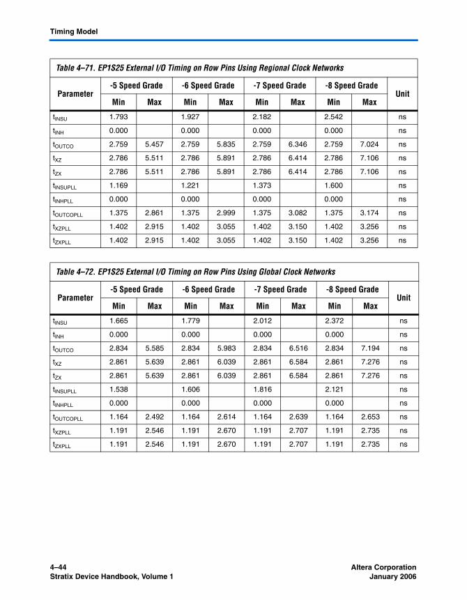
4–44 Altera CorporationStratix Device Handbook, Volume 1 January 2006
Timing Model
Table 4–71. EP1S25 External I/O Timing on Row Pins Using Regional Clock Networks
Parameter-5 Speed Grade -6 Speed Grade -7 Speed Grade -8 Speed Grade
UnitMin Max Min Max Min Max Min Max
tINSU 1.793 1.927 2.182 2.542 ns
tINH 0.000 0.000 0.000 0.000 ns
tOUTCO 2.759 5.457 2.759 5.835 2.759 6.346 2.759 7.024 ns
tXZ 2.786 5.511 2.786 5.891 2.786 6.414 2.786 7.106 ns
tZX 2.786 5.511 2.786 5.891 2.786 6.414 2.786 7.106 ns
tINSUPLL 1.169 1.221 1.373 1.600 ns
tINHPLL 0.000 0.000 0.000 0.000 ns
tOUTCOPLL 1.375 2.861 1.375 2.999 1.375 3.082 1.375 3.174 ns
tXZPLL 1.402 2.915 1.402 3.055 1.402 3.150 1.402 3.256 ns
tZXPLL 1.402 2.915 1.402 3.055 1.402 3.150 1.402 3.256 ns
Table 4–72. EP1S25 External I/O Timing on Row Pins Using Global Clock Networks
Parameter-5 Speed Grade -6 Speed Grade -7 Speed Grade -8 Speed Grade
UnitMin Max Min Max Min Max Min Max
tINSU 1.665 1.779 2.012 2.372 ns
tINH 0.000 0.000 0.000 0.000 ns
tOUTCO 2.834 5.585 2.834 5.983 2.834 6.516 2.834 7.194 ns
tXZ 2.861 5.639 2.861 6.039 2.861 6.584 2.861 7.276 ns
tZX 2.861 5.639 2.861 6.039 2.861 6.584 2.861 7.276 ns
tINSUPLL 1.538 1.606 1.816 2.121 ns
tINHPLL 0.000 0.000 0.000 0.000 ns
tOUTCOPLL 1.164 2.492 1.164 2.614 1.164 2.639 1.164 2.653 ns
tXZPLL 1.191 2.546 1.191 2.670 1.191 2.707 1.191 2.735 ns
tZXPLL 1.191 2.546 1.191 2.670 1.191 2.707 1.191 2.735 ns

Altera Corporation 4–45January 2006 Stratix Device Handbook, Volume 1
DC & Switching Characteristics
Tables 4–73 through 4–78 show the external timing parameters on column and row pins for EP1S30 devices.
Table 4–73. EP1S30 External I/O Timing on Column Pins Using Fast Regional Clock Networks
Parameter-5 Speed Grade -6 Speed Grade -7 Speed Grade -8 Speed Grade Unit
Min Max Min Max Min Max Min Max
tINSU 2.502 2.680 3.062 3.591 ns
tINH 0.000 0.000 0.000 0.000 ns
tOUTCO 2.473 4.965 2.473 5.329 2.473 5.784 2.473 6.392 ns
tXZ 2.413 4.839 2.413 5.197 2.413 5.660 2.413 6.277 ns
tZX 2.413 4.839 2.413 5.197 2.413 5.660 2.413 6.277 ns
Table 4–74. EP1S30 External I/O Timing on Column Pins Using Regional Clock Networks
Parameter-5 Speed Grade -6 Speed Grade -7 Speed Grade -8 Speed Grade
UnitMin Max Min Max Min Max Min Max
tINSU 2.286 2.426 2.769 3.249 ns
tINH 0.000 0.000 0.000 0.000 ns
tOUTCO 2.641 5.225 2.641 5.629 2.641 6.130 2.641 6.796 ns
tXZ 2.581 5.099 2.581 5.497 2.581 6.006 2.581 6.681 ns
tZX 2.581 5.099 2.581 5.497 2.581 6.006 2.581 6.681 ns
tINSUPLL 1.200 1.185 1.344 1.662 ns
tINHPLL 0.000 0.000 0.000 0.000 ns
tOUTCOPLL 1.108 2.367 1.108 2.534 1.108 2.569 1.108 2.517 ns
tXZPLL 1.048 2.241 1.048 2.402 1.048 2.445 1.048 2.402 ns
tZXPLL 1.048 2.241 1.048 2.402 1.048 2.445 1.048 2.402 ns
Table 4–75. EP1S30 External I/O Timing on Column Pins Using Global Clock Networks (Part 1 of 2)
Parameter-5 Speed Grade -6 Speed Grade -7 Speed Grade -8 Speed Grade
UnitMin Max Min Max Min Max Min Max
tINSU 1.935 2.029 2.310 2.709 ns
tINH 0.000 0.000 0.000 0.000 ns
tOUTCO 2.814 5.532 2.814 5.980 2.814 6.536 2.814 7.274 ns

4–46 Altera CorporationStratix Device Handbook, Volume 1 January 2006
Timing Model
tXZ 2.754 5.406 2.754 5.848 2.754 6.412 2.754 7.159 ns
tZX 2.754 5.406 2.754 5.848 2.754 6.412 2.754 7.159 ns
tINSUPLL 1.265 1.236 1.403 1.756 ns
tINHPLL 0.000 0.000 0.000 0.000 ns
tOUTCOPLL 1.068 2.302 1.068 2.483 1.068 2.510 1.068 2.423 ns
tXZPLL 1.008 2.176 1.008 2.351 1.008 2.386 1.008 2.308 ns
tZXPLL 1.008 2.176 1.008 2.351 1.008 2.386 1.008 2.308 ns
Table 4–76. EP1S30 External I/O Timing on Row Pins Using Fast Regional Clock Networks
Parameters-5 Speed Grade -6 Speed Grade -7 Speed Grade -8 Speed Grade
UnitMin Max Min Max Min Max Min Max
tINSU 2.616 2.808 3.223 3.797 ns
tINH 0.000 0.000 0.000 0.000 ns
tOUTCO 2.542 5.114 2.542 5.502 2.542 5.965 2.542 6.581 ns
tXZ 2.569 5.168 2.569 5.558 2.569 6.033 2.569 6.663 ns
tZX 2.569 5.168 2.569 5.558 2.569 6.033 2.569 6.663 ns
Table 4–75. EP1S30 External I/O Timing on Column Pins Using Global Clock Networks (Part 2 of 2)
Parameter-5 Speed Grade -6 Speed Grade -7 Speed Grade -8 Speed Grade
UnitMin Max Min Max Min Max Min Max

Altera Corporation 4–47January 2006 Stratix Device Handbook, Volume 1
DC & Switching Characteristics
Table 4–77. EP1S30 External I/O Timing on Row Pins Using Regional Clock Networks
Parameter-5 Speed Grade -6 Speed Grade -7 Speed Grade -8 Speed Grade
UnitMin Max Min Max Min Max Min Max
tINSU 2.322 2.467 2.828 3.342 ns
tINH 0.000 0.000 0.000 0.000 ns
tOUTCO 2.731 5.408 2.731 5.843 2.731 6.360 2.731 7.036 ns
tXZ 2.758 5.462 2.758 5.899 2.758 6.428 2.758 7.118 ns
tZX 2.758 5.462 2.758 5.899 2.758 6.428 2.758 7.118 ns
tINSUPLL 1.291 1.283 1.469 1.832 ns
tINHPLL 0.000 0.000 0.000 0.000 ns
tOUTCOPLL 1.192 2.539 1.192 2.737 1.192 2.786 1.192 2.742 ns
tXZPLL 1.219 2.539 1.219 2.793 1.219 2.854 1.219 2.824 ns
tZXPLL 1.219 2.539 1.219 2.793 1.219 2.854 1.219 2.824 ns
Table 4–78. EP1S30 External I/O Timing on Row Pins Using Global Clock Networks
Parameter-5 Speed Grade -6 Speed Grade -7 Speed Grade -8 Speed Grade
UnitMin Max Min Max Min Max Min Max
tINSU 1.995 2.089 2.398 2.830 ns
tINH 0.000 0.000 0.000 0.000 ns
tOUTCO 2.917 5.735 2.917 6.221 2.917 6.790 2.917 7.548 ns
tXZ 2.944 5.789 2.944 6.277 2.944 6.858 2.944 7.630 ns
tZX 2.944 5.789 2.944 6.277 2.944 6.858 2.944 7.630 ns
tINSUPLL 1.337 1.312 1.508 1.902 ns
tINHPLL 0.000 0.000 0.000 0.000 ns
tOUTCOPLL 1.164 2.493 1.164 2.708 1.164 2.747 1.164 2.672 ns
tXZPLL 1.191 2.547 1.191 2.764 1.191 2.815 1.191 2.754 ns
tZXPLL 1.191 2.547 1.191 2.764 1.191 2.815 1.191 2.754 ns
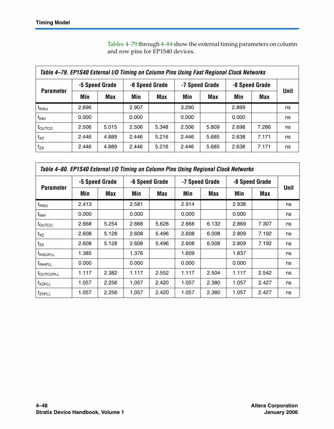
4–48 Altera CorporationStratix Device Handbook, Volume 1 January 2006
Timing Model
Tables 4–79 through 4–84 show the external timing parameters on column and row pins for EP1S40 devices.
Table 4–79. EP1S40 External I/O Timing on Column Pins Using Fast Regional Clock Networks
Parameter-5 Speed Grade -6 Speed Grade -7 Speed Grade -8 Speed Grade
UnitMin Max Min Max Min Max Min Max
tINSU 2.696 2.907 3.290 2.899 ns
tINH 0.000 0.000 0.000 0.000 ns
tOUTCO 2.506 5.015 2.506 5.348 2.506 5.809 2.698 7.286 ns
tXZ 2.446 4.889 2.446 5.216 2.446 5.685 2.638 7.171 ns
tZX 2.446 4.889 2.446 5.216 2.446 5.685 2.638 7.171 ns
Table 4–80. EP1S40 External I/O Timing on Column Pins Using Regional Clock Networks
Parameter-5 Speed Grade -6 Speed Grade -7 Speed Grade -8 Speed Grade
UnitMin Max Min Max Min Max Min Max
tINSU 2.413 2.581 2.914 2.938 ns
tINH 0.000 0.000 0.000 0.000 ns
tOUTCO 2.668 5.254 2.668 5.628 2.668 6.132 2.869 7.307 ns
tXZ 2.608 5.128 2.608 5.496 2.608 6.008 2.809 7.192 ns
tZX 2.608 5.128 2.608 5.496 2.608 6.008 2.809 7.192 ns
tINSUPLL 1.385 1.376 1.609 1.837 ns
tINHPLL 0.000 0.000 0.000 0.000 ns
tOUTCOPLL 1.117 2.382 1.117 2.552 1.117 2.504 1.117 2.542 ns
tXZPLL 1.057 2.256 1,057 2.420 1.057 2.380 1.057 2.427 ns
tZXPLL 1.057 2.256 1,057 2.420 1.057 2.380 1.057 2.427 ns

Altera Corporation 4–49January 2006 Stratix Device Handbook, Volume 1
DC & Switching Characteristics
Table 4–81. EP1S40 External I/O Timing on Column Pins Using Global Clock Networks
Parameter-5 Speed Grade -6 Speed Grade -7 Speed Grade -8 Speed Grade
UnitMin Max Min Max Min Max Min Max
tINSU 2.126 2.268 2.558 2.930 ns
tINH 0.000 0.000 0.000 0.000 ns
tOUTCO 2.856 5.585 2.856 5.987 2.856 6.541 2.847 7.253 ns
tXZ 2.796 5.459 2.796 5.855 2.796 6.417 2.787 7.138 ns
tZX 2.796 5.459 2.796 5.855 2.796 6.417 2.787 7.138 ns
tINSUPLL 1.466 1.455 1.711 1.906 ns
tINHPLL 0.000 0.000 0.000 0.000 ns
tOUTCOPLL 1.092 2.345 1.092 2.510 1.092 2.455 1.089 2.473 ns
tXZPLL 1.032 2.219 1.032 2.378 1.032 2.331 1.029 2.358 ns
tZXPLL 1.032 2.219 1.032 2.378 1.032 2.331 1.029 2.358 ns
Table 4–82. EP1S40 External I/O Timing on Row Pins Using Fast Regional Clock Networks
Parameter-5 Speed Grade -6 Speed Grade -7 Speed Grade -8 Speed Grade
UnitMin Max Min Max Min Max Min Max
tINSU 2.472 2.685 3.083 3.056 ns
tINH 0.000 0.000 0.000 0.000 ns
tOUTCO 2.631 5.258 2.631 5.625 2.631 6.105 2.745 7.324 ns
tXZ 2.658 5.312 2.658 5.681 2.658 6.173 2.772 7.406 ns
tZX 2.658 5.312 2.658 5.681 2.658 6.173 2.772 7.406 ns

4–50 Altera CorporationStratix Device Handbook, Volume 1 January 2006
Timing Model
Table 4–83. EP1S40 External I/O Timing on Row Pins Using Regional Clock Networks
Parameter-5 Speed Grade -6 Speed Grade -7 Speed Grade -8 Speed Grade
UnitMin Max Min Max Min Max Min Max
tINSU 2.349 2.526 2.898 2.952 ns
tINH 0.000 0.000 0.000 0.000 ns
tOUTCO 2.725 5.381 2.725 5.784 2.725 6.290 2.725 7.426 ns
tXZ 2.752 5.435 2.752 5.840 2.752 6.358 2.936 7.508 ns
tZX 2.752 5.435 2.752 5.840 2.752 6.358 2.936 7.508 ns
tINSUPLL 1.328 1.322 1.605 1.883 ns
tINHPLL 0.000 0.000 0.000 0.000 ns
tOUTCOPLL 1.169 2.502 1.169 2.698 1.169 2.650 1.169 2.691 ns
tXZPLL 1.196 2.556 1.196 2.754 1.196 2.718 1.196 2.773 ns
tZXPLL 1.196 2.556 1.196 2.754 1.196 2.718 1.196 2.773 ns
Table 4–84. EP1S40 External I/O Timing on Row Pins Using Global Clock Networks
Parameter-5 Speed Grade -6 Speed Grade -7 Speed Grade -8 Speed Grade
UnitMin Max Min Max Min Max Min Max
tINSU 2.020 2.171 2.491 2.898 ns
tINH 0.000 0.000 0.000 0.000 ns
tOUTCO 2.912 5.710 2.912 6.139 2.912 6.697 2.931 7.480 ns
tXZ 2.939 5.764 2.939 6.195 2.939 6.765 2.958 7.562 ns
tZX 2.939 5.764 2.939 6.195 2.939 6.765 2.958 7.562 ns
tINSUPLL 1.370 1.368 1.654 1.881 ns
tINHPLL 0.000 0.000 0.000 0.000 ns
tOUTCOPLL 1.144 2.460 1.144 2.652 1.144 2.601 1.170 2.693 ns
tXZPLL 1.171 2.514 1.171 2.708 1.171 2.669 1.197 2.775 ns
tZXPLL 1.171 2.514 1.171 2.708 1.171 2.669 1.197 2.775 ns

Altera Corporation 4–51January 2006 Stratix Device Handbook, Volume 1
DC & Switching Characteristics
Tables 4–85 through 4–90 show the external timing parameters on column and row pins for EP1S60 devices.
Table 4–85. EP1S60 External I/O Timing on Column Pins Using Fast Regional Clock Networks Note (1)
Parameter-5 Speed Grade -6 Speed Grade -7 Speed Grade -8 Speed Grade
UnitMin Max Min Max Min Max Min Max
tINSU 3.029 3.277 3.733 NA ns
tINH 0.000 0.000 0.000 NA ns
tOUTCO 2.446 4.871 2.446 5.215 2.446 5.685 NA NA ns
tXZ 2.386 4.745 2.386 5.083 2.386 5.561 NA NA ns
tZX 2.386 4.745 2.386 5.083 2.386 5.561 NA NA ns
Table 4–86. EP1S60 External I/O Timing on Column Pins Using Regional Clock Networks Note (1)
Parameter-5 Speed Grade -6 Speed Grade -7 Speed Grade -8 Speed Grade
UnitMin Max Min Max Min Max Min Max
tINSU 2.491 2.691 3.060 NA ns
tINH 0.000 0.000 0.000 NA ns
tOUTCO 2.767 5.409 2.767 5.801 2.767 6.358 NA NA ns
tXZ 2.707 5.283 2.707 5.669 2.707 6.234 NA NA ns
tZX 2.707 5.283 2.707 5.669 2.707 6.234 NA NA ns
tINSUPLL 1.233 1.270 1.438 NA ns
tINHPLL 0.000 0.000 0.000 NA ns
tOUTCOPLL 1.078 2.278 1.078 2.395 1.078 2.428 NA NA ns
tXZPLL 1.018 2.152 1.018 2.263 1.018 2.304 NA NA ns
tZXPLL 1.018 2.152 1.018 2.263 1.018 2.304 NA NA ns

4–52 Altera CorporationStratix Device Handbook, Volume 1 January 2006
Timing Model
Table 4–87. EP1S60 External I/O Timing on Column Pins Using Global Clock Networks Note (1)
Parameter-5 Speed Grade -6 Speed Grade -7 Speed Grade -8 Speed Grade
UnitMin Max Min Max Min Max Min Max
tINSU 2.000 2.152 2.441 NA ns
tINH 0.000 0.000 0.000 NA ns
tOUTCO 3.051 5.900 3.051 6.340 3.051 6.977 NA NA ns
tXZ 2.991 5.774 2.991 6.208 2.991 6.853 NA NA ns
tZX 2.991 5.774 2.991 6.208 2.991 6.853 NA NA ns
tINSUPLL 1.315 1.362 1.543 NA ns
tINHPLL 0.000 0.000 0.000 NA ns
tOUTCOPLL 1.029 2.196 1.029 2.303 1.029 2.323 NA NA ns
tXZPLL 0.969 2.070 0.969 2.171 0.969 2.199 NA NA ns
tZXPLL 0.969 2.070 0.969 2.171 0.969 2.199 NA NA ns
Table 4–88. EP1S60 External I/O Timing on Row Pins Using Fast Regional Clock Networks Note (1)
Parameter-5 Speed Grade -6 Speed Grade -7 Speed Grade -8 Speed Grade
UnitMin Max Min Max Min Max Min Max
tINSU 3.144 3.393 3.867 NA ns
tINH 0.000 0.000 0.000 NA ns
tOUTCO 2.643 5.275 2.643 5.654 2.643 6.140 NA NA ns
tXZ 2.670 5.329 2.670 5.710 2.670 6.208 NA NA ns
tZX 2.670 5.329 2.670 5.710 2.670 6.208 NA NA ns
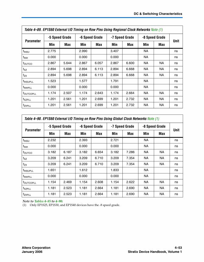
Altera Corporation 4–53January 2006 Stratix Device Handbook, Volume 1
DC & Switching Characteristics
Table 4–89. EP1S60 External I/O Timing on Row Pins Using Regional Clock Networks Note (1)
Parameter-5 Speed Grade -6 Speed Grade -7 Speed Grade -8 Speed Grade
UnitMin Max Min Max Min Max Min Max
tINSU 2.775 2.990 3.407 NA ns
tINH 0.000 0.000 0.000 NA ns
tOUTCO 2.867 5.644 2.867 6.057 2.867 6.600 NA NA ns
tXZ 2.894 5.698 2.894 6.113 2.894 6.668 NA NA ns
tZX 2.894 5.698 2.894 6.113 2.894 6.668 NA NA ns
tINSUPLL 1.523 1.577 1.791 NA ns
tINHPLL 0.000 0.000 0.000 NA ns
tOUTCOPLL 1.174 2.507 1.174 2.643 1.174 2.664 NA NA ns
tXZPLL 1.201 2.561 1.201 2.699 1.201 2.732 NA NA ns
tZXPLL 1.201 2.561 1.201 2.699 1.201 2.732 NA NA ns
Table 4–90. EP1S60 External I/O Timing on Row Pins Using Global Clock Networks Note (1)
Parameter-5 Speed Grade -6 Speed Grade -7 Speed Grade -8 Speed Grade
UnitMin Max Min Max Min Max Min Max
tINSU 2.232 2.393 2.721 NA ns
tINH 0.000 0.000 0.000 NA ns
tOUTCO 3.182 6.187 3.182 6.654 3.182 7.286 NA NA ns
tXZ 3.209 6.241 3.209 6.710 3.209 7.354 NA NA ns
tZX 3.209 6.241 3.209 6.710 3.209 7.354 NA NA ns
tINSUPLL 1.651 1.612 1.833 NA ns
tINHPLL 0.000 0.000 0.000 NA ns
tOUTCOPLL 1.154 2.469 1.154 2.608 1.154 2.622 NA NA ns
tXZPLL 1.181 2.523 1.181 2.664 1.181 2.690 NA NA ns
tZXPLL 1.181 2.523 1.181 2.664 1.181 2.690 NA NA ns
Note to Tables 4–85 to 4–90:(1) Only EP1S25, EP1S30, and EP1S40 devices have the -8 speed grade.
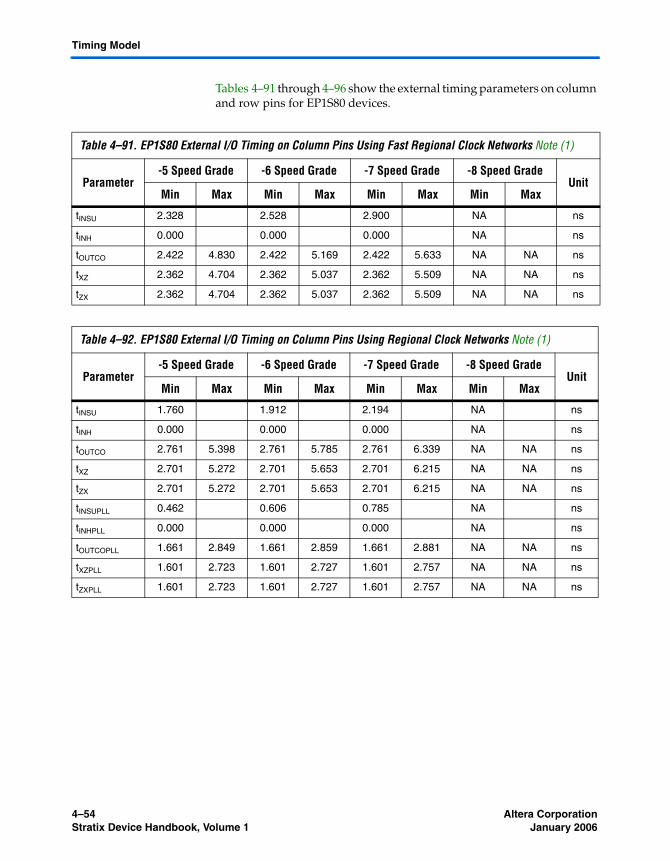
4–54 Altera CorporationStratix Device Handbook, Volume 1 January 2006
Timing Model
Tables 4–91 through 4–96 show the external timing parameters on column and row pins for EP1S80 devices.
Table 4–91. EP1S80 External I/O Timing on Column Pins Using Fast Regional Clock Networks Note (1)
Parameter-5 Speed Grade -6 Speed Grade -7 Speed Grade -8 Speed Grade
UnitMin Max Min Max Min Max Min Max
tINSU 2.328 2.528 2.900 NA ns
tINH 0.000 0.000 0.000 NA ns
tOUTCO 2.422 4.830 2.422 5.169 2.422 5.633 NA NA ns
tXZ 2.362 4.704 2.362 5.037 2.362 5.509 NA NA ns
tZX 2.362 4.704 2.362 5.037 2.362 5.509 NA NA ns
Table 4–92. EP1S80 External I/O Timing on Column Pins Using Regional Clock Networks Note (1)
Parameter-5 Speed Grade -6 Speed Grade -7 Speed Grade -8 Speed Grade
UnitMin Max Min Max Min Max Min Max
tINSU 1.760 1.912 2.194 NA ns
tINH 0.000 0.000 0.000 NA ns
tOUTCO 2.761 5.398 2.761 5.785 2.761 6.339 NA NA ns
tXZ 2.701 5.272 2.701 5.653 2.701 6.215 NA NA ns
tZX 2.701 5.272 2.701 5.653 2.701 6.215 NA NA ns
tINSUPLL 0.462 0.606 0.785 NA ns
tINHPLL 0.000 0.000 0.000 NA ns
tOUTCOPLL 1.661 2.849 1.661 2.859 1.661 2.881 NA NA ns
tXZPLL 1.601 2.723 1.601 2.727 1.601 2.757 NA NA ns
tZXPLL 1.601 2.723 1.601 2.727 1.601 2.757 NA NA ns

Altera Corporation 4–55January 2006 Stratix Device Handbook, Volume 1
DC & Switching Characteristics
Table 4–93. EP1S80 External I/O Timing on Column Pins Using Global Clock Networks Note (1)
Parameter-5 Speed Grade -6 Speed Grade -7 Speed Grade -8 Speed Grade
UnitMin Max Min Max Min Max Min Max
tINSU 0.884 0.976 1.118 NA ns
tINH 0.000 0.000 0.000 NA ns
tOUTCO 3.267 6.274 3.267 6.721 3.267 7.415 NA NA ns
tXZ 3.207 6.148 3.207 6.589 3.207 7.291 NA NA ns
tZX 3.207 6.148 3.207 6.589 3.207 7.291 NA NA ns
tINSUPLL 0.506 0.656 0.838 NA ns
tINHPLL 0.000 0.000 0.000 NA ns
tOUTCOPLL 1.635 2.805 1.635 2.809 1.635 2.828 NA NA ns
tXZPLL 1.575 2.679 1.575 2.677 1.575 2.704 NA NA ns
tZXPLL 1.575 2.679 1.575 2.677 1.575 2.704 NA NA ns
Table 4–94. EP1S80 External I/O Timing on Row Pins Using Fast Regional Clock Networks Note (1)
Parameter-5 Speed Grade -6 Speed Grade -7 Speed Grade -8 Speed Grade
Unit
Min Max Min Max Min Max Min Max
tINSU 2.792 2.993 3.386 NA ns
tINH 0.000 0.000 0.000 NA ns
tOUTCO 2.619 5.235 2.619 5.609 2.619 6.086 NA NA ns
tXZ 2.646 5.289 2.646 5.665 2.646 6.154 NA NA ns
tZX 2.646 5.289 2.646 5.665 2.646 6.154 NA NA ns

4–56 Altera CorporationStratix Device Handbook, Volume 1 January 2006
Timing Model
Table 4–95. EP1S80 External I/O Timing on Row Pins Using Regional Clock Networks Note (1)
Parameter-5 Speed Grade -6 Speed Grade -7 Speed Grade -8 Speed Grade
Unit
Min Max Min Max Min Max Min Max
tINSU 2.295 2.454 2.767 NA ns
tINH 0.000 0.000 0.000 NA ns
tOUTCO 2.917 5.732 2.917 6.148 2.917 6.705 NA NA ns
tXZ 2.944 5.786 2.944 6.204 2.944 6.773 NA NA ns
tZX 2.944 5.786 2.944 6.204 2.944 6.773 NA NA ns
tINSUPLL 1.011 1.161 1.372 NA ns
tINHPLL 0.000 0.000 0.000 NA ns
tOUTCOPLL 1.808 3.169 1.808 3.209 1.808 3.233 NA NA ns
tXZPLL 1.835 3.223 1.835 3.265 1.835 3.301 NA NA ns
tZXPLL 1.835 3.223 1.835 3.265 1.835 3.301 NA NA ns
Table 4–96. EP1S80 External I/O Timing on Rows Using Pin Global Clock Networks Note (1)
Symbol-5 Speed Grade -6 Speed Grade -7 Speed Grade -8 Speed Grade
UnitMin Max Min Max Min Max Min Max
tINSU 1.362 1.451 1.613 NA ns
tINH 0.000 0.000 0.000 NA ns
tOUTCO 3.457 6.665 3.457 7.151 3.457 7.859 NA NA ns
tXZ 3.484 6.719 3.484 7.207 3.484 7.927 NA NA ns
tZX 3.484 6.719 3.484 7.207 3.484 7.927 NA NA ns
tINSUPLL o.994 1.143 1.351 NA ns
tINHPLL 0.000 0.000 0.000 NA ns
tOUTCOPLL 1.821 3.186 1.821 3.227 1.821 3.254 NA NA ns
tXZPLL 1.848 3.240 1.848 3.283 1.848 3.322 NA NA ns
tZXPLL 1.848 3.240 1.848 3.283 1.848 3.322 NA NA ns
Note to Tables 4–91 to 4–96:(1) Only EP1S25, EP1S30, and EP1S40 devices have the -8 speed grade.
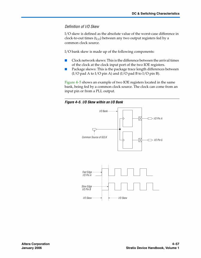
Altera Corporation 4–57January 2006 Stratix Device Handbook, Volume 1
DC & Switching Characteristics
Definition of I/O Skew
I/O skew is defined as the absolute value of the worst-case difference in clock-to-out times (tCO) between any two output registers fed by a common clock source.
I/O bank skew is made up of the following components:
■ Clock network skews: This is the difference between the arrival times of the clock at the clock input port of the two IOE registers.
■ Package skews: This is the package trace length differences between (I/O pad A to I/O pin A) and (I/O pad B to I/O pin B).
Figure 4–5 shows an example of two IOE registers located in the same bank, being fed by a common clock source. The clock can come from an input pin or from a PLL output.
Figure 4–5. I/O Skew within an I/O Bank
Common Source of GCLK
Fast Edge
Slow Edge
I/O Skew
I/O Bank
I/O Skew
I/O Pin A
I/O Pin B
I/O Pin A
I/O Pin B

4–58 Altera CorporationStratix Device Handbook, Volume 1 January 2006
Timing Model
Figure 4–6 shows the case where four IOE registers are located in two different I/O banks.
Figure 4–6. I/O Skew Across Two I/O Banks
Table 4–97 defines the timing parameters used to define the timing for horizontal I/O pins (side banks 1, 2, 5, 6) and vertical I/O pins (top and bottom banks 3, 4, 7, 8). The timing parameters define the skew within an I/O bank, across two neighboring I/O banks on the same side of the device, across all horizontal I/O banks, across all vertical I/O banks, and the skew for the overall device.
Table 4–97. Output Pin Timing Skew Definitions (Part 1 of 2)
Symbol Definition
tSB_HIO Row I/O (HIO) within one I/O bank (1)
tSB_VIO Column I/O (VIO) within one I/O bank (1)
tSS_HIO Row I/O (HIO) same side of the device, across two banks (2)
tSS_VIO Column I/O (VIO) same side of the device, across two banks (2)
Common Source of GCLK
I/O Bank
I/O Bank
I/O Pin A
I/O Pin B
I/O Pin C
I/O Pin D
I/O Pin A
I/O Pin B
I/O Pin C
I/O Pin D
I/O Pin Skew acrosstwo Banks
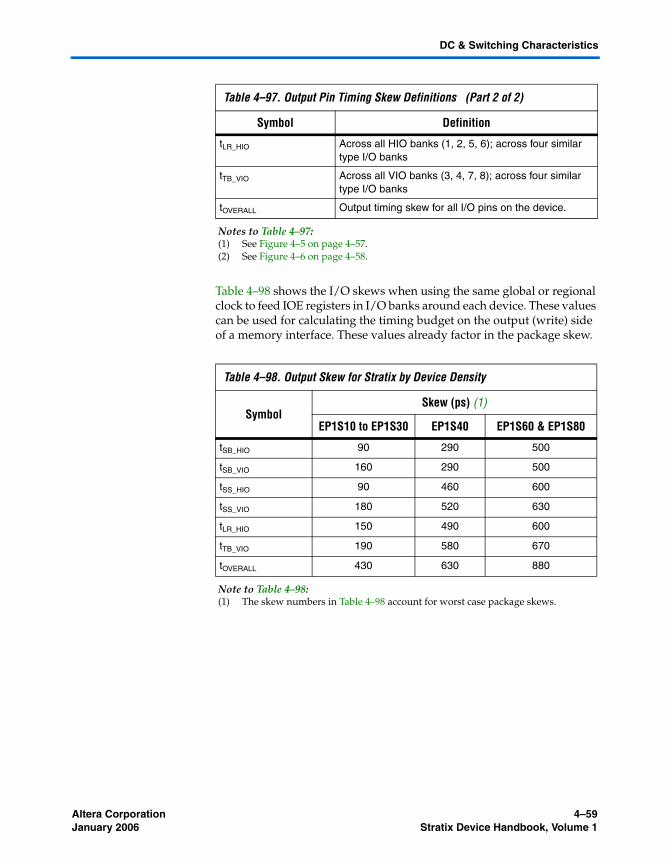
Altera Corporation 4–59January 2006 Stratix Device Handbook, Volume 1
DC & Switching Characteristics
Table 4–98 shows the I/O skews when using the same global or regional clock to feed IOE registers in I/O banks around each device. These values can be used for calculating the timing budget on the output (write) side of a memory interface. These values already factor in the package skew.
tLR_HIO Across all HIO banks (1, 2, 5, 6); across four similar type I/O banks
tTB_VIO Across all VIO banks (3, 4, 7, 8); across four similar type I/O banks
tOVERALL Output timing skew for all I/O pins on the device.
Notes to Table 4–97:(1) See Figure 4–5 on page 4–57.(2) See Figure 4–6 on page 4–58.
Table 4–98. Output Skew for Stratix by Device Density
SymbolSkew (ps) (1)
EP1S10 to EP1S30 EP1S40 EP1S60 & EP1S80
tSB_HIO 90 290 500
tSB_VIO 160 290 500
tSS_HIO 90 460 600
tSS_VIO 180 520 630
tLR_HIO 150 490 600
tTB_VIO 190 580 670
tOVERALL 430 630 880
Note to Table 4–98:(1) The skew numbers in Table 4–98 account for worst case package skews.
Table 4–97. Output Pin Timing Skew Definitions (Part 2 of 2)
Symbol Definition
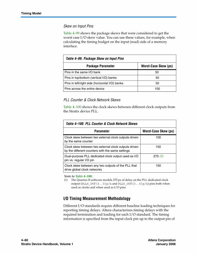
4–60 Altera CorporationStratix Device Handbook, Volume 1 January 2006
Timing Model
Skew on Input Pins
Table 4–99 shows the package skews that were considered to get the worst case I/O skew value. You can use these values, for example, when calculating the timing budget on the input (read) side of a memory interface.
PLL Counter & Clock Network Skews
Table 4–100 shows the clock skews between different clock outputs from the Stratix device PLL.
I/O Timing Measurement Methodology
Different I/O standards require different baseline loading techniques for reporting timing delays. Altera characterizes timing delays with the required termination and loading for each I/O standard. The timing information is specified from the input clock pin up to the output pin of
Table 4–99. Package Skew on Input Pins
Package Parameter Worst-Case Skew (ps)
Pins in the same I/O bank 50
Pins in top/bottom (vertical I/O) banks 50
Pins in left/right side (horizontal I/O) banks 50
Pins across the entire device 100
Table 4–100. PLL Counter & Clock Network Skews
Parameter Worst-Case Skew (ps)
Clock skew between two external clock outputs driven by the same counter
100
Clock skew between two external clock outputs driven by the different counters with the same settings
150
Dual-purpose PLL dedicated clock output used as I/O pin vs. regular I/O pin
270 (1)
Clock skew between any two outputs of the PLL that drive global clock networks
150
Note to Table 4–100:(1) The Quartus II software models 270 ps of delay on the PLL dedicated clock
output (PLL6_OUT[3..0]p/n and PLL5_OUT[3..0]p/n) pins both when used as clocks and when used as I/O pins.
Altera Corporation 4–61January 2006 Stratix Device Handbook, Volume 1
DC & Switching Characteristics
the FPGA device. The Quartus II software calculates the I/O timing for each I/O standard with a default baseline loading as specified by the I/O standard.
Altera measures clock-to-output delays (tCO) at worst-case process, minimum voltage, and maximum temperature (PVT) for the 3.3-V LVTTL I/O standard with 24 mA (default case) current drive strength setting and fast slew rate setting. I/O adder delays are measured to calculate the tCO change at worst-case PVT across all I/O standards and current drive strength settings with the default loading shown in Table 4–101 on page 4–62. Timing derating data for additional loading is taken for tCO across worst-case PVT for all I/O standards and drive strength settings. These three pieces of data are used to predict the timing at the output pin.
tCO at pin = tOUTCO max for 3.3-V 24 mA LVTTL + I/O Adder + Output Delay Adder for Loading
Simulation using IBIS models is required to determine the delays on the PCB traces in addition to the output pin delay timing reported by the Quartus II software and the timing model in the device handbook.
1. Simulate the output driver of choice into the generalized test setup using values from Table 4–101 on page 4–62.
2. Record the time to VMEAS.
3. Simulate the output driver of choice into the actual PCB trace and load, using the appropriate IBIS input buffer model or an equivalent capacitance value to represent the load.
4. Record the time to VMEAS.
5. Compare the results of steps 2 and 4. The increase or decrease in delay should be added to or subtracted from the I/O Standard Output Adder delays to yield the actual worst-case propagation delay (clock-to-input) of the PCB trace.
The Quartus II software reports maximum timing with the conditions shown in Table 4–101 on page 4–62 using the proceeding equation. Figure 4–7 on page 4–62 shows the model of the circuit that is represented by the Quartus II output timing.

4–62 Altera CorporationStratix Device Handbook, Volume 1 January 2006
Timing Model
Figure 4–7. Output Delay Timing Reporting Setup Modeled by Quartus II
Notes to Figure 4–7:(1) Output pin timing is reported at the output pin of the FPGA device. Additional
delays for loading and board trace delay need to be accounted for with IBIS model simulations.
(2) VCCINT is 1.42-V unless otherwise specified.
VCCIO
GND
OUTPUT
GND
RT
VTT
RS
CL
OutputBuffer
Single-Ended Outputs
VMEAS
GND
RUP
VCCIO
RDN
Table 4–101. Reporting Methodology For Maximum Timing For Single-Ended Output Pins (Part 1 of 2) Notes (1), (2), (3)
I/O Standard
Loading and Termination Measurement Point
RUP
ΩRDN
ΩRS
ΩRT
ΩVCCIO
(V)VTT(V)
CL
(pF)VMEAS
3.3-V LVTTL – – 0 – 2.950 2.95 10 1.500
2.5-V LVTTL – – 0 – 2.370 2.37 10 1.200
1.8-V LVTTL – – 0 – 1.650 1.65 10 0.880
1.5-V LVTTL – – 0 – 1.400 1.40 10 0.750
3.3-V LVCMOS – – 0 – 2.950 2.95 10 1.500
2.5-V LVCMOS – – 0 – 2.370 2.37 10 1.200
1.8-V LVCMOS – – 0 – 1.650 1.65 10 0.880
1.5-V LVCMOS – – 0 – 1.400 1.40 10 0.750
3.3-V GTL – – 0 25 2.950 1.14 30 0.740
2.5-V GTL – – 0 25 2.370 1.14 30 0.740
3.3-V GTL+ – – 0 25 2.950 1.35 30 0.880
2.5-V GTL+ – – 0 25 2.370 1.35 30 0.880
3.3-V SSTL-3 Class II – – 25 25 2.950 1.25 30 1.250

Altera Corporation 4–63January 2006 Stratix Device Handbook, Volume 1
DC & Switching Characteristics
3.3-V SSTL-3 Class I – – 25 50 2.950 1.250 30 1.250
2.5-V SSTL-2 Class II – – 25 25 2.370 1.110 30 1.110
2.5-V SSTL-2 Class I – – 25 50 2.370 1.110 30 1.110
1.8-V SSTL-18 Class II – – 25 25 1.650 0.760 30 0.760
1.8-V SSTL-18 Class I – – 25 50 1.650 0.760 30 0.760
1.5-V HSTL Class II – – 0 25 1.400 0.700 20 0.680
1.5-V HSTL Class I – – 0 50 1.400 0.700 20 0.680
1.8-V HSTL Class II – – 0 25 1.650 0.700 20 0.880
1.8-V HSTL Class I – – 0 50 1.650 0.700 20 0.880
3.3-V PCI (4) –/25 25/– 0 – 2.950 2.950 10 0.841/1.814
3.3-V PCI-X 1.0 (4) –/25 25/– 0 – 2.950 2.950 10 0.841/1.814
3.3-V Compact PCI (4) –/25 25/– 0 – 2.950 2.950 10 0.841/1.814
3.3-V AGP 1X (4) –/25 25/– 0 – 2.950 2.950 10 0.841/1.814
3.3-V CTT – – 25 50 2.050 1.350 30 1.350
Notes to Table 4–101:(1) Input measurement point at internal node is 0.5 × VCCINT.(2) Output measuring point for data is VMEAS.(3) Input stimulus edge rate is 0 to VCCINT in 0.5 ns (internal signal) from the driver preceding the IO buffer.(4) The first value is for output rising edge and the second value is for output falling edge. The hyphen (-) indicates
infinite resistance or disconnection.
Table 4–101. Reporting Methodology For Maximum Timing For Single-Ended Output Pins (Part 2 of 2) Notes (1), (2), (3)
I/O Standard
Loading and Termination Measurement Point
RUP
ΩRDN
ΩRS
ΩRT
ΩVCCIO
(V)VTT(V)
CL
(pF)VMEAS

4–64 Altera CorporationStratix Device Handbook, Volume 1 January 2006
Timing Model
Table 4–102 shows the reporting methodology used by the Quartus II software for minimum timing information for output pins.
Table 4–102. Reporting Methodology For Minimum Timing For Single-Ended Output Pins (Part 1 of 2) Notes (1), (2), (3)
I/O Standard
Loading and Termination Measurement Point
RUP
ΩRDN
ΩRS
ΩRT
ΩVCCIO
(V)VTT(V)
CL
(pF)VMEAS
3.3-V LVTTL – – 0 – 3.600 3.600 10 1.800
2.5-V LVTTL – – 0 – 2.630 2.630 10 1.200
1.8-V LVTTL – – 0 – 1.950 1.950 10 0.880
1.5-V LVTTL – – 0 – 1.600 1.600 10 0.750
3.3-V LVCMOS – – 0 – 3.600 3.600 10 1.800
2.5-V LVCMOS – – 0 – 2.630 2.630 10 1.200
1.8-V LVCMOS – – 0 – 1.950 1.950 10 0.880
1.5-V LVCMOS – – 0 – 1.600 1.600 10 0.750
3.3-V GTL – – 0 25 3.600 1.260 30 0.860
2.5-V GTL – – 0 25 2.630 1.260 30 0.860
3.3-V GTL+ – – 0 25 3.600 1.650 30 1.120
2.5-V GTL+ – – 0 25 2.630 1.650 30 1.120
3.3-V SSTL-3 Class II – – 25 25 3.600 1.750 30 1.750
3.3-V SSTL-3 Class I – – 25 50 3.600 1.750 30 1.750
2.5-V SSTL-2 Class II – – 25 25 2.630 1.390 30 1.390
2.5-V SSTL-2 Class I – – 25 50 2.630 1.390 30 1.390
1.8-V SSTL-18 Class II – – 25 25 1.950 1.040 30 1.040
1.8-V SSTL-18 Class I – – 25 50 1.950 1.040 30 1.040
1.5-V HSTL Class II – – 0 25 1.600 0.800 20 0.900
1.5-V HSTL Class I – – 0 50 1.600 0.800 20 0.900
1.8-V HSTL Class II – – 0 25 1.950 0.900 20 1.000
1.8-V HSTL Class I – – 0 50 1.950 0.900 20 1.000
3.3-V PCI (4) –/25 25/– 0 – 3.600 1.950 10 1.026/2.214
3.3-V PCI-X 1.0 (4) –/25 25/– 0 – 3.600 1.950 10 1.026/2.214
3.3-V Compact PCI (4) –/25 25/– 0 – 3.600 3.600 10 1.026/2.214
3.3-V AGP 1× (4) –/25 25/– 0 – 3.600 3.600 10 1.026/2.214

Altera Corporation 4–65January 2006 Stratix Device Handbook, Volume 1
DC & Switching Characteristics
Figure 4–8 shows the measurement setup for output disable and output enable timing. The TCHZ stands for clock to high Z time delay and is the same as TXZ. The TCLZ stands for clock to low Z (driving) time delay and is the same as TZX.
Figure 4–8. Measurement Setup for TXZ and TZX
3.3-V CTT – – 25 50 3.600 1.650 30 1.650
Notes to Table 4–102:(1) Input measurement point at internal node is 0.5 × VCCINT.(2) Output measuring point for data is VMEAS. When two values are given, the first is the measurement point on the
rising edge and the other is for the falling edge.(3) Input stimulus edge rate is 0 to VCCINT in 0.5 ns (internal signal) from the driver preceding the I/O buffer.(4) The first value is for the output rising edge and the second value is for the output falling edge. The hyphen (-)
indicates infinite resistance or disconnection.
Table 4–102. Reporting Methodology For Minimum Timing For Single-Ended Output Pins (Part 2 of 2) Notes (1), (2), (3)
I/O Standard
Loading and Termination Measurement Point
RUP
ΩRDN
ΩRS
ΩRT
ΩVCCIO
(V)VTT(V)
CL
(pF)VMEAS
200mV
200mV 200mV
200mV
CLK
OUT
OUT
T CHZ
T CLZ
V T =1.5V
C TOTAL=10pF
R =50Ω

4–66 Altera CorporationStratix Device Handbook, Volume 1 January 2006
Timing Model
External I/O Delay Parameters
External I/O delay timing parameters for I/O standard input and output adders and programmable input and output delays are specified by speed grade independent of device density. All of the timing parameters in this section apply to both flip-chip and wire-bond packages.
Tables 4–103 and 4–104 show the input adder delays associated with column and row I/O pins. If an I/O standard is selected other than 3.3-V LVTTL or LVCMOS, add the selected delay to the external tINSU and tINSUPLL I/O parameters shown in Tables 4–54 through 4–96.
Table 4–103. Stratix I/O Standard Column Pin Input Delay Adders
Parameter-5 Speed Grade -6 Speed Grade -7 Speed Grade -8 Speed Grade
UnitMin Max Min Max Min Max Min Max
LVCMOS 0 0 0 0 ps
3.3-V LVTTL 0 0 0 0 ps
2.5-V LVTTL 19 19 22 26 ps
1.8-V LVTTL 221 232 266 313 ps
1.5-V LVTTL 352 369 425 500 ps
GTL –45 –48 –55 –64 ps
GTL+ –75 –79 –91 –107 ps
3.3-V PCI 0 0 0 0 ps
3.3-V PCI-X 1.0 0 0 0 0 ps
Compact PCI 0 0 0 0 ps
AGP 1× 0 0 0 0 ps
AGP 2× 0 0 0 0 ps
CTT 120 126 144 170 ps
SSTL-3 Class I –162 –171 –196 –231 ps
SSTL-3 Class II –162 –171 –196 –231 ps
SSTL-2 Class I –202 –213 –244 –287 ps
SSTL-2 Class II –202 –213 –244 –287 ps
SSTL-18 Class I 78 81 94 110 ps
SSTL-18 Class II 78 81 94 110 ps
1.5-V HSTL Class I –76 –80 –92 –108 ps
1.5-V HSTL Class II –76 –80 –92 –108 ps
1.8-V HSTL Class I –52 –55 –63 –74 ps
1.8-V HSTL Class II –52 –55 –63 –74 ps
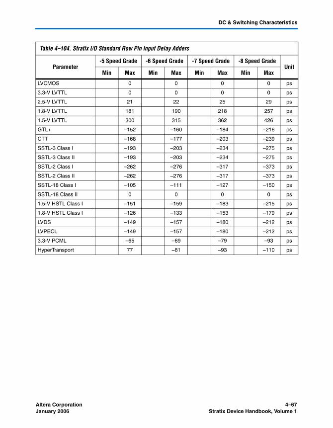
Altera Corporation 4–67January 2006 Stratix Device Handbook, Volume 1
DC & Switching Characteristics
Table 4–104. Stratix I/O Standard Row Pin Input Delay Adders
Parameter-5 Speed Grade -6 Speed Grade -7 Speed Grade -8 Speed Grade
UnitMin Max Min Max Min Max Min Max
LVCMOS 0 0 0 0 ps
3.3-V LVTTL 0 0 0 0 ps
2.5-V LVTTL 21 22 25 29 ps
1.8-V LVTTL 181 190 218 257 ps
1.5-V LVTTL 300 315 362 426 ps
GTL+ –152 –160 –184 –216 ps
CTT –168 –177 –203 –239 ps
SSTL-3 Class I –193 –203 –234 –275 ps
SSTL-3 Class II –193 –203 –234 –275 ps
SSTL-2 Class I –262 –276 –317 –373 ps
SSTL-2 Class II –262 –276 –317 –373 ps
SSTL-18 Class I –105 –111 –127 –150 ps
SSTL-18 Class II 0 0 0 0 ps
1.5-V HSTL Class I –151 –159 –183 –215 ps
1.8-V HSTL Class I –126 –133 –153 –179 ps
LVDS –149 –157 –180 –212 ps
LVPECL –149 –157 –180 –212 ps
3.3-V PCML –65 –69 –79 –93 ps
HyperTransport 77 –81 –93 –110 ps
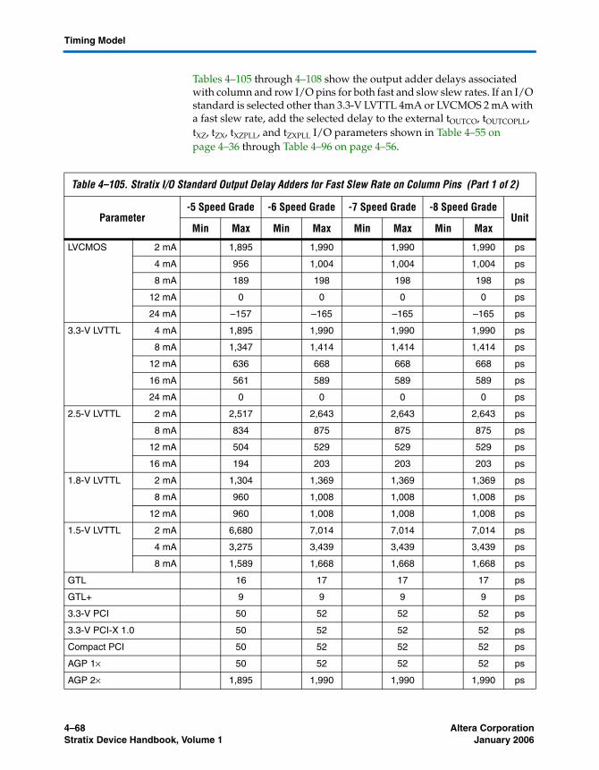
4–68 Altera CorporationStratix Device Handbook, Volume 1 January 2006
Timing Model
Tables 4–105 through 4–108 show the output adder delays associated with column and row I/O pins for both fast and slow slew rates. If an I/O standard is selected other than 3.3-V LVTTL 4mA or LVCMOS 2 mA with a fast slew rate, add the selected delay to the external tOUTCO, tOUTCOPLL, tXZ, tZX, tXZPLL, and tZXPLL I/O parameters shown in Table 4–55 on page 4–36 through Table 4–96 on page 4–56.
Table 4–105. Stratix I/O Standard Output Delay Adders for Fast Slew Rate on Column Pins (Part 1 of 2)
Parameter-5 Speed Grade -6 Speed Grade -7 Speed Grade -8 Speed Grade
UnitMin Max Min Max Min Max Min Max
LVCMOS 2 mA 1,895 1,990 1,990 1,990 ps
4 mA 956 1,004 1,004 1,004 ps
8 mA 189 198 198 198 ps
12 mA 0 0 0 0 ps
24 mA –157 –165 –165 –165 ps
3.3-V LVTTL 4 mA 1,895 1,990 1,990 1,990 ps
8 mA 1,347 1,414 1,414 1,414 ps
12 mA 636 668 668 668 ps
16 mA 561 589 589 589 ps
24 mA 0 0 0 0 ps
2.5-V LVTTL 2 mA 2,517 2,643 2,643 2,643 ps
8 mA 834 875 875 875 ps
12 mA 504 529 529 529 ps
16 mA 194 203 203 203 ps
1.8-V LVTTL 2 mA 1,304 1,369 1,369 1,369 ps
8 mA 960 1,008 1,008 1,008 ps
12 mA 960 1,008 1,008 1,008 ps
1.5-V LVTTL 2 mA 6,680 7,014 7,014 7,014 ps
4 mA 3,275 3,439 3,439 3,439 ps
8 mA 1,589 1,668 1,668 1,668 ps
GTL 16 17 17 17 ps
GTL+ 9 9 9 9 ps
3.3-V PCI 50 52 52 52 ps
3.3-V PCI-X 1.0 50 52 52 52 ps
Compact PCI 50 52 52 52 ps
AGP 1× 50 52 52 52 ps
AGP 2× 1,895 1,990 1,990 1,990 ps

Altera Corporation 4–69January 2006 Stratix Device Handbook, Volume 1
DC & Switching Characteristics
CTT 973 1,021 1,021 1,021 ps
SSTL-3 Class I 719 755 755 755 ps
SSTL-3 Class II 146 153 153 153 ps
SSTL-2 Class I 678 712 712 712 ps
SSTL-2 Class II 223 234 234 234 ps
SSTL-18 Class I 1,032 1,083 1,083 1,083 ps
SSTL-18 Class II 447 469 469 469 ps
1.5-V HSTL Class I 660 693 693 693 ps
1.5-V HSTL Class II 537 564 564 564 ps
1.8-V HSTL Class I 304 319 319 319 ps
1.8-V HSTL Class II 231 242 242 242 ps
Table 4–106. Stratix I/O Standard Output Delay Adders for Fast Slew Rate on Row Pins (Part 1 of 2)
Parameter-5 Speed Grade -6 Speed Grade -7 Speed Grade -8 Speed Grade
UnitMin Max Min Max Min Max Min Max
LVCMOS 2 mA 1,518 1,594 1,594 1,594 ps
4 mA 746 783 783 783 ps
8 mA 96 100 100 100 ps
12 mA 0 0 0 0 ps
3.3-V LVTTL 4 mA 1,518 1,594 1,594 1,594 ps
8 mA 1,038 1,090 1,090 1,090 ps
12 mA 521 547 547 547 ps
16 mA 414 434 434 434 ps
24 mA 0 0 0 0 ps
2.5-V LVTTL 2 mA 2,032 2,133 2,133 2,133 ps
8 mA 699 734 734 734 ps
12 mA 374 392 392 392 ps
16 mA 165 173 173 173 ps
1.8-V LVTTL 2 mA 3,714 3,899 3,899 3,899 ps
8 mA 1,055 1,107 1,107 1,107 ps
12 mA 830 871 871 871 ps
Table 4–105. Stratix I/O Standard Output Delay Adders for Fast Slew Rate on Column Pins (Part 2 of 2)
Parameter-5 Speed Grade -6 Speed Grade -7 Speed Grade -8 Speed Grade
UnitMin Max Min Max Min Max Min Max
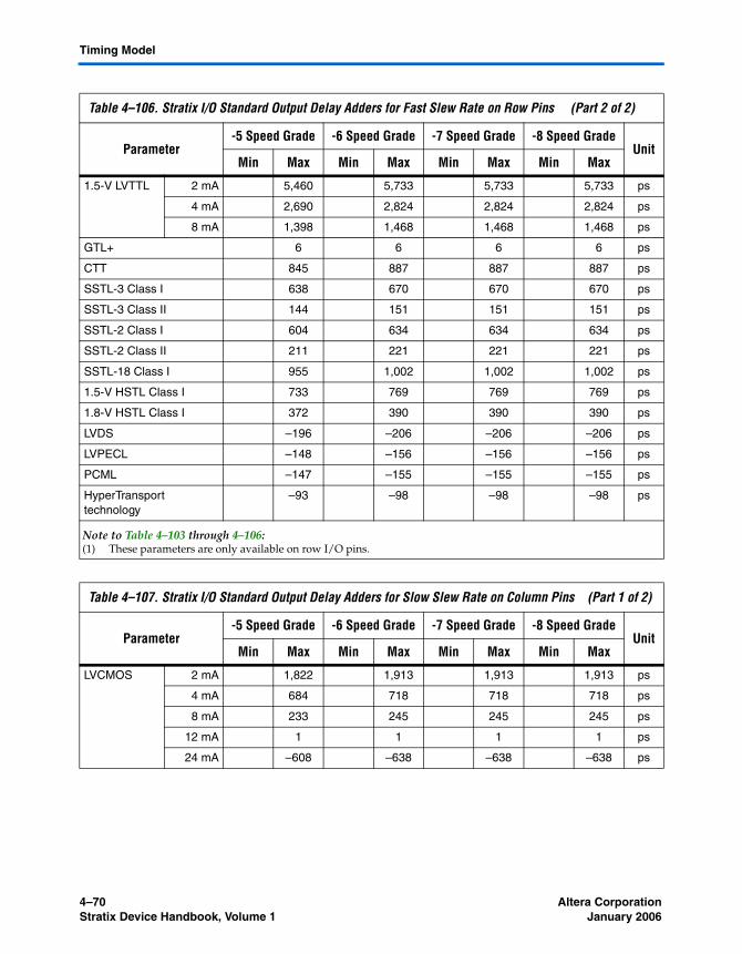
4–70 Altera CorporationStratix Device Handbook, Volume 1 January 2006
Timing Model
1.5-V LVTTL 2 mA 5,460 5,733 5,733 5,733 ps
4 mA 2,690 2,824 2,824 2,824 ps
8 mA 1,398 1,468 1,468 1,468 ps
GTL+ 6 6 6 6 ps
CTT 845 887 887 887 ps
SSTL-3 Class I 638 670 670 670 ps
SSTL-3 Class II 144 151 151 151 ps
SSTL-2 Class I 604 634 634 634 ps
SSTL-2 Class II 211 221 221 221 ps
SSTL-18 Class I 955 1,002 1,002 1,002 ps
1.5-V HSTL Class I 733 769 769 769 ps
1.8-V HSTL Class I 372 390 390 390 ps
LVDS –196 –206 –206 –206 ps
LVPECL –148 –156 –156 –156 ps
PCML –147 –155 –155 –155 ps
HyperTransport technology
–93 –98 –98 –98 ps
Note to Table 4–103 through 4–106:(1) These parameters are only available on row I/O pins.
Table 4–107. Stratix I/O Standard Output Delay Adders for Slow Slew Rate on Column Pins (Part 1 of 2)
Parameter-5 Speed Grade -6 Speed Grade -7 Speed Grade -8 Speed Grade
UnitMin Max Min Max Min Max Min Max
LVCMOS 2 mA 1,822 1,913 1,913 1,913 ps
4 mA 684 718 718 718 ps
8 mA 233 245 245 245 ps
12 mA 1 1 1 1 ps
24 mA –608 –638 –638 –638 ps
Table 4–106. Stratix I/O Standard Output Delay Adders for Fast Slew Rate on Row Pins (Part 2 of 2)
Parameter-5 Speed Grade -6 Speed Grade -7 Speed Grade -8 Speed Grade
UnitMin Max Min Max Min Max Min Max
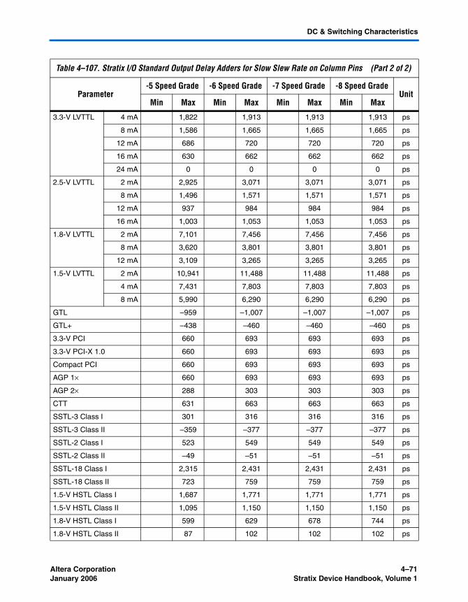
Altera Corporation 4–71January 2006 Stratix Device Handbook, Volume 1
DC & Switching Characteristics
3.3-V LVTTL 4 mA 1,822 1,913 1,913 1,913 ps
8 mA 1,586 1,665 1,665 1,665 ps
12 mA 686 720 720 720 ps
16 mA 630 662 662 662 ps
24 mA 0 0 0 0 ps
2.5-V LVTTL 2 mA 2,925 3,071 3,071 3,071 ps
8 mA 1,496 1,571 1,571 1,571 ps
12 mA 937 984 984 984 ps
16 mA 1,003 1,053 1,053 1,053 ps
1.8-V LVTTL 2 mA 7,101 7,456 7,456 7,456 ps
8 mA 3,620 3,801 3,801 3,801 ps
12 mA 3,109 3,265 3,265 3,265 ps
1.5-V LVTTL 2 mA 10,941 11,488 11,488 11,488 ps
4 mA 7,431 7,803 7,803 7,803 ps
8 mA 5,990 6,290 6,290 6,290 ps
GTL –959 –1,007 –1,007 –1,007 ps
GTL+ –438 –460 –460 –460 ps
3.3-V PCI 660 693 693 693 ps
3.3-V PCI-X 1.0 660 693 693 693 ps
Compact PCI 660 693 693 693 ps
AGP 1× 660 693 693 693 ps
AGP 2× 288 303 303 303 ps
CTT 631 663 663 663 ps
SSTL-3 Class I 301 316 316 316 ps
SSTL-3 Class II –359 –377 –377 –377 ps
SSTL-2 Class I 523 549 549 549 ps
SSTL-2 Class II –49 –51 –51 –51 ps
SSTL-18 Class I 2,315 2,431 2,431 2,431 ps
SSTL-18 Class II 723 759 759 759 ps
1.5-V HSTL Class I 1,687 1,771 1,771 1,771 ps
1.5-V HSTL Class II 1,095 1,150 1,150 1,150 ps
1.8-V HSTL Class I 599 629 678 744 ps
1.8-V HSTL Class II 87 102 102 102 ps
Table 4–107. Stratix I/O Standard Output Delay Adders for Slow Slew Rate on Column Pins (Part 2 of 2)
Parameter-5 Speed Grade -6 Speed Grade -7 Speed Grade -8 Speed Grade
UnitMin Max Min Max Min Max Min Max

4–72 Altera CorporationStratix Device Handbook, Volume 1 January 2006
Timing Model
Table 4–108. Stratix I/O Standard Output Delay Adders for Slow Slew Rate on Row Pins
I/O Standard-5 Speed Grade -6 Speed Grade -7 Speed Grade -8 Speed Grade
UnitMin Max Min Max Min Max Min Max
LVCMOS 2 mA 1,571 1,650 1,650 1,650 ps
4 mA 594 624 624 624 ps
8 mA 208 218 218 218 ps
12 mA 0 0 0 0 ps
3.3-V LVTTL 4 mA 1,571 1,650 1,650 1,650 ps
8 mA 1,393 1,463 1,463 1,463 ps
12 mA 596 626 626 626 ps
16 mA 562 590 590 590 ps
2.5-V LVTTL 2 mA 2,562 2,690 2,690 2,690 ps
8 mA 1,343 1,410 1,410 1,410 ps
12 mA 864 907 907 907 ps
16 mA 945 992 992 992 ps
1.8-V LVTTL 2 mA 6,306 6,621 6,621 6,621 ps
8 mA 3,369 3,538 3,538 3,538 ps
12 mA 2,932 3,079 3,079 3,079 ps
1.5-V LVTTL 2 mA 9,759 10,247 10,247 10,247 ps
4 mA 6,830 7,172 7,172 7,172 ps
8 mA 5,699 5,984 5,984 5,984 ps
GTL+ –333 –350 –350 –350 ps
CTT 591 621 621 621 ps
SSTL-3 Class I 267 280 280 280 ps
SSTL-3 Class II –346 –363 –363 –363 ps
SSTL-2 Class I 481 505 505 505 ps
SSTL-2 Class II –58 –61 –61 –61 ps
SSTL-18 Class I 2,207 2,317 2,317 2,317 ps
1.5-V HSTL Class I 1,966 2,064 2,064‘ 2,064 ps
1.8-V HSTL Class I 1,208 1,268 1,460 1,720 ps

Altera Corporation 4–73January 2006 Stratix Device Handbook, Volume 1
DC & Switching Characteristics
Tables 4–109 and 4–110 show the adder delays for the column and row IOE programmable delays. These delays are controlled with the Quartus II software logic options listed in the Parameter column.
Table 4–109. Stratix IOE Programmable Delays on Column Pins Note (1)
Parameter Setting-5 Speed Grade -6 Speed Grade -7 Speed Grade -8 Speed Grade
UnitMin Max Min Max Min Max Min Max
Decrease input delay to internal cells
Off 3,970 4,367 5,022 5,908 ps
Small 3,390 3,729 4,288 5,045 ps
Medium 2,810 3,091 3,554 4,181 ps
Large 224 235 270 318 ps
On 224 235 270 318 ps
Decrease input delay to input register
Off 3,900 4,290 4,933 5,804 ps
On 0 0 0 0 ps
Decrease input delay to output register
Off 1,240 1,364 1,568 1,845 ps
On 0 0 0 0 ps
Increase delay to output pin
Off 0 0 0 0 ps
On 397 417 417 417 ps
Increase delay to output enable pin
Off 0 0 0 0 ps
On 338 372 427 503 ps
Increase output clock enable delay
Off 0 0 0 0 ps
Small 540 594 683 804 ps
Large 1,016 1,118 1,285 1,512 ps
On 1,016 1,118 1,285 1,512 ps
Increase input clock enable delay
Off 0 0 0 0 ps
Small 540 594 683 804 ps
Large 1,016 1,118 1,285 1,512 ps
On 1,016 1,118 1,285 1,512 ps
Increase output enable clock enable delay
Off 0 0 0 0 ps
Small 540 594 683 804 ps
Large 1,016 1,118 1,285 1,512 ps
On 1,016 1,118 1,285 1,512 ps
Increase tZX delay to output pin
Off 0 0 0 0 ps
On 2,199 2,309 2,309 2,309 ps

4–74 Altera CorporationStratix Device Handbook, Volume 1 January 2006
Timing Model
Table 4–110. Stratix IOE Programmable Delays on Row Pins Note (1)
Parameter Setting-5 Speed Grade -6 Speed Grade -7 Speed Grade -8 Speed Grade
UnitMin Max Min Max Min Max Min Max
Decrease input delay to internal cells
Off 3,970 4,367 5,022 5,908 ps
Small 3,390 3,729 4,288 5,045 ps
Medium 2,810 3,091 3,554 4,181 ps
Large 173 181 208 245 ps
On 173 181 208 245 ps
Decrease input delay to input register
Off 3,900 4,290 4,933 5,804 ps
On 0 0 0 0 ps
Decrease input delay to output register
Off 1,240 1,364 1,568 1,845 ps
On 0 0 0 0 ps
Increase delay to output pin
Off 0 0 0 0 ps
On 397 417 417 417 ps
Increase delay to output enable pin
Off 0 0 0 0 ps
On 348 383 441 518 ps
Increase output clock enable delay
Off 0 0 0 0 ps
Small 180 198 227 267 ps
Large 260 286 328 386 ps
On 260 286 328 386 ps
Increase input clock enable delay
Off 0 0 0 0 ps
Small 180 198 227 267 ps
Large 260 286 328 386 ps
On 260 286 328 386 ps
Increase output enable clock enable delay
Off 0 0 0 0 ps
Small 540 594 683 804 ps
Large 1,016 1,118 1,285 1,512 ps
On 1,016 1,118 1,285 1,512 ps
Increase tZX delay to output pin
Off 0 0 0 0 ps
On 1,993 2,092 2,092 2,092 ps
Note to Table 4–109 and Table 4–110:(1) The delay chain delays vary for different device densities. These timing values only apply to EP1S30 and EP1S40
devices. Reference the timing information reported by the Quartus II software for other devices.

Altera Corporation 4–75January 2006 Stratix Device Handbook, Volume 1
DC & Switching Characteristics
The scaling factors for column output pin timing in Tables 4–111 to 4–113 are shown in units of time per pF unit of capacitance (ps/pF). Add this delay to the tCO or combinatorial timing path for output or bidirectional pins in addition to the I/O adder delays shown in Tables 4–103 through 4–108 and the IOE programmable delays in Tables 4–109 and 4–110.
Table 4–111. Output Delay Adder for Loading on LVTTL/LVCMOS Output Buffers Note (1)
Conditions Output Pin Adder Delay (ps/pF)
Parameter Value 3.3-V LVTTL 2.5-V LVTTL 1.8-V LVTTL 1.5-V LVTTL LVCMOS
Drive Strength
24mA 15 – – - 8
16mA 25 18 – – –
12mA 30 25 25 – 15
8mA 50 35 40 35 20
4mA 60 – – 80 30
2mA – 75 120 160 60
Note to Table 4–111:(1) The timing information in this table is preliminary.
Table 4–112. Output Delay Adder for Loading on SSTL/HSTL Output Buffers Note (1)
ConditionsOutput Pin Adder Delay (ps/pF)
SSTL-3 SSTL-2 SSTL-1.8 1.5-V HSTL
Class IClass II
25 25 25 25
25 20 25 20
Note to Table 4–112:(1) The timing information in this table is preliminary.
Table 4–113. Output Delay Adder for Loading on GTL+/GTL/CTT/PCI Output Buffers Note (1)
Conditions Output Pin Adder Delay (ps/pF)
Parameter Value GTL+ GTL CTT PCI AGP
VCCIO Voltage Level
3.3V 18 18 25 20 20
2.5V 15 18 - - -
Note to Table 4–113:(1) The timing information in this table is preliminary.

4–76 Altera CorporationStratix Device Handbook, Volume 1 January 2006
Timing Model
Maximum Input & Output Clock Rates
Tables 4–114 through 4–119 show the maximum input clock rate for column and row pins in Stratix devices.
Table 4–114. Stratix Maximum Input Clock Rate for CLK[7..4] & CLK[15..12] Pins in Flip-Chip Packages (Part 1 of 2)
I/O Standard -5 Speed Grade
-6 Speed Grade
-7 Speed Grade
-8 Speed Grade Unit
LVTTL 422 422 390 390 MHz
2.5 V 422 422 390 390 MHz
1.8 V 422 422 390 390 MHz
1.5 V 422 422 390 390 MHz
LVCMOS 422 422 390 390 MHz
GTL 300 250 200 200 MHz
GTL+ 300 250 200 200 MHz
SSTL-3 Class I 400 350 300 300 MHz
SSTL-3 Class II 400 350 300 300 MHz
SSTL-2 Class I 400 350 300 300 MHz
SSTL-2 Class II 400 350 300 300 MHz
SSTL-18 Class I 400 350 300 300 MHz
SSTL-18 Class II 400 350 300 300 MHz
1.5-V HSTL Class I 400 350 300 300 MHz
1.5-V HSTL Class II 400 350 300 300 MHz
1.8-V HSTL Class I 400 350 300 300 MHz
1.8-V HSTL Class II 400 350 300 300 MHz
3.3-V PCI 422 422 390 390 MHz
3.3-V PCI-X 1.0 422 422 390 390 MHz
Compact PCI 422 422 390 390 MHz
AGP 1× 422 422 390 390 MHz
AGP 2× 422 422 390 390 MHz
CTT 300 250 200 200 MHz
Differential 1.5-V HSTL C1
400 350 300 300 MHz
LVPECL (1) 645 645 622 622 MHz
PCML (1) 300 275 275 275 MHz

Altera Corporation 4–77January 2006 Stratix Device Handbook, Volume 1
DC & Switching Characteristics
LVDS (1) 645 645 622 622 MHz
HyperTransport technology (1)
500 500 450 450 MHz
Table 4–115. Stratix Maximum Input Clock Rate for CLK[0, 2, 9, 11] Pins & FPLL[10..7]CLK Pins in Flip-Chip Packages
I/O Standard -5 Speed Grade
-6 Speed Grade
-7 Speed Grade
-8 Speed Grade Unit
LVTTL 422 422 390 390 MHz
2.5 V 422 422 390 390 MHz
1.8 V 422 422 390 390 MHz
1.5 V 422 422 390 390 MHz
LVCMOS 422 422 390 390 MHz
GTL+ 300 250 200 200 MHz
SSTL-3 Class I 400 350 300 300 MHz
SSTL-3 Class II 400 350 300 300 MHz
SSTL-2 Class I 400 350 300 300 MHz
SSTL-2 Class II 400 350 300 300 MHz
SSTL-18 Class I 400 350 300 300 MHz
SSTL-18 Class II 400 350 300 300 MHz
1.5-V HSTL Class I 400 350 300 300 MHz
1.8-V HSTL Class I 400 350 300 300 MHz
CTT 300 250 200 200 MHz
Differential 1.5-V HSTL C1
400 350 300 300 MHz
LVPECL (1) 717 717 640 640 MHz
PCML (1) 400 375 350 350 MHz
LVDS (1) 717 717 640 640 MHz
HyperTransport technology (1)
717 717 640 640 MHz
Table 4–114. Stratix Maximum Input Clock Rate for CLK[7..4] & CLK[15..12] Pins in Flip-Chip Packages (Part 2 of 2)
I/O Standard -5 Speed Grade
-6 Speed Grade
-7 Speed Grade
-8 Speed Grade Unit
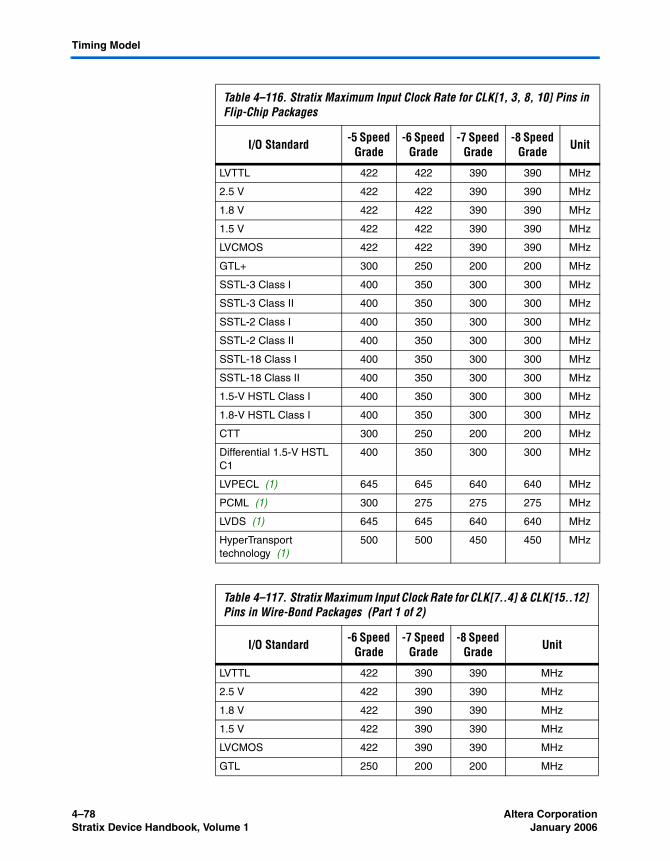
4–78 Altera CorporationStratix Device Handbook, Volume 1 January 2006
Timing Model
Table 4–116. Stratix Maximum Input Clock Rate for CLK[1, 3, 8, 10] Pins in Flip-Chip Packages
I/O Standard -5 Speed Grade
-6 Speed Grade
-7 Speed Grade
-8 Speed Grade Unit
LVTTL 422 422 390 390 MHz
2.5 V 422 422 390 390 MHz
1.8 V 422 422 390 390 MHz
1.5 V 422 422 390 390 MHz
LVCMOS 422 422 390 390 MHz
GTL+ 300 250 200 200 MHz
SSTL-3 Class I 400 350 300 300 MHz
SSTL-3 Class II 400 350 300 300 MHz
SSTL-2 Class I 400 350 300 300 MHz
SSTL-2 Class II 400 350 300 300 MHz
SSTL-18 Class I 400 350 300 300 MHz
SSTL-18 Class II 400 350 300 300 MHz
1.5-V HSTL Class I 400 350 300 300 MHz
1.8-V HSTL Class I 400 350 300 300 MHz
CTT 300 250 200 200 MHz
Differential 1.5-V HSTL C1
400 350 300 300 MHz
LVPECL (1) 645 645 640 640 MHz
PCML (1) 300 275 275 275 MHz
LVDS (1) 645 645 640 640 MHz
HyperTransport technology (1)
500 500 450 450 MHz
Table 4–117. Stratix Maximum Input Clock Rate for CLK[7..4] & CLK[15..12] Pins in Wire-Bond Packages (Part 1 of 2)
I/O Standard -6 Speed Grade
-7 Speed Grade
-8 Speed Grade Unit
LVTTL 422 390 390 MHz
2.5 V 422 390 390 MHz
1.8 V 422 390 390 MHz
1.5 V 422 390 390 MHz
LVCMOS 422 390 390 MHz
GTL 250 200 200 MHz
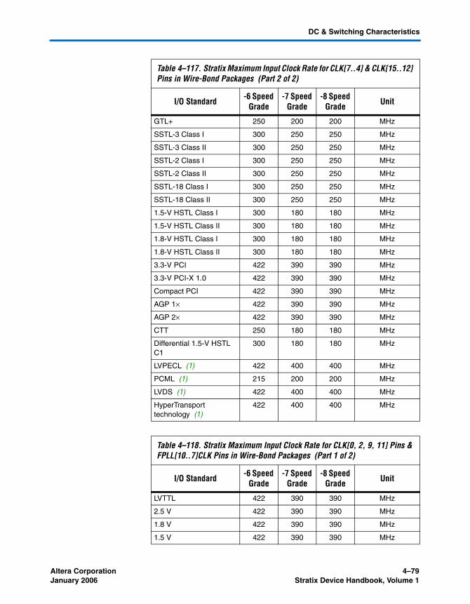
Altera Corporation 4–79January 2006 Stratix Device Handbook, Volume 1
DC & Switching Characteristics
GTL+ 250 200 200 MHz
SSTL-3 Class I 300 250 250 MHz
SSTL-3 Class II 300 250 250 MHz
SSTL-2 Class I 300 250 250 MHz
SSTL-2 Class II 300 250 250 MHz
SSTL-18 Class I 300 250 250 MHz
SSTL-18 Class II 300 250 250 MHz
1.5-V HSTL Class I 300 180 180 MHz
1.5-V HSTL Class II 300 180 180 MHz
1.8-V HSTL Class I 300 180 180 MHz
1.8-V HSTL Class II 300 180 180 MHz
3.3-V PCI 422 390 390 MHz
3.3-V PCI-X 1.0 422 390 390 MHz
Compact PCI 422 390 390 MHz
AGP 1× 422 390 390 MHz
AGP 2× 422 390 390 MHz
CTT 250 180 180 MHz
Differential 1.5-V HSTL C1
300 180 180 MHz
LVPECL (1) 422 400 400 MHz
PCML (1) 215 200 200 MHz
LVDS (1) 422 400 400 MHz
HyperTransport technology (1)
422 400 400 MHz
Table 4–118. Stratix Maximum Input Clock Rate for CLK[0, 2, 9, 11] Pins & FPLL[10..7]CLK Pins in Wire-Bond Packages (Part 1 of 2)
I/O Standard -6 Speed Grade
-7 Speed Grade
-8 Speed Grade Unit
LVTTL 422 390 390 MHz
2.5 V 422 390 390 MHz
1.8 V 422 390 390 MHz
1.5 V 422 390 390 MHz
Table 4–117. Stratix Maximum Input Clock Rate for CLK[7..4] & CLK[15..12] Pins in Wire-Bond Packages (Part 2 of 2)
I/O Standard -6 Speed Grade
-7 Speed Grade
-8 Speed Grade Unit

4–80 Altera CorporationStratix Device Handbook, Volume 1 January 2006
Timing Model
LVCMOS 422 390 390 MHz
GTL+ 250 200 200 MHz
SSTL-3 Class I 350 300 300 MHz
SSTL-3 Class II 350 300 300 MHz
SSTL-2 Class I 350 300 300 MHz
SSTL-2 Class II 350 300 300 MHz
SSTL-18 Class I 350 300 300 MHz
SSTL-18 Class II 350 300 300 MHz
1.5-V HSTL Class I 350 300 300 MHz
1.8-V HSTL Class I 350 300 300 MHz
CTT 250 200 200 MHz
Differential 1.5-V HSTL C1
350 300 300 MHz
LVPECL (1) 717 640 640 MHz
PCML (1) 375 350 350 MHz
LVDS (1) 717 640 640 MHz
HyperTransport technology (1)
717 640 640 MHz
Table 4–119. Stratix Maximum Input Clock Rate for CLK[1, 3, 8, 10] Pins in Wire-Bond Packages (Part 1 of 2)
I/O Standard -6 Speed Grade
-7 Speed Grade
-8 Speed Grade Unit
LVTTL 422 390 390 MHz
2.5 V 422 390 390 MHz
1.8 V 422 390 390 MHz
1.5 V 422 390 390 MHz
LVCMOS 422 390 390 MHz
GTL+ 250 200 200 MHz
SSTL-3 Class I 350 300 300 MHz
SSTL-3 Class II 350 300 300 MHz
SSTL-2 Class I 350 300 300 MHz
SSTL-2 Class II 350 300 300 MHz
Table 4–118. Stratix Maximum Input Clock Rate for CLK[0, 2, 9, 11] Pins & FPLL[10..7]CLK Pins in Wire-Bond Packages (Part 2 of 2)
I/O Standard -6 Speed Grade
-7 Speed Grade
-8 Speed Grade Unit
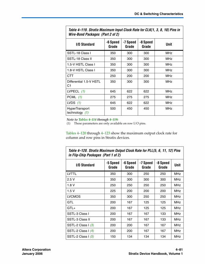
Altera Corporation 4–81January 2006 Stratix Device Handbook, Volume 1
DC & Switching Characteristics
Tables 4–120 through 4–123 show the maximum output clock rate for column and row pins in Stratix devices.
SSTL-18 Class I 350 300 300 MHz
SSTL-18 Class II 350 300 300 MHz
1.5-V HSTL Class I 350 300 300 MHz
1.8-V HSTL Class I 350 300 300 MHz
CTT 250 200 200 MHz
Differential 1.5-V HSTL C1
350 300 300 MHz
LVPECL (1) 645 622 622 MHz
PCML (1) 275 275 275 MHz
LVDS (1) 645 622 622 MHz
HyperTransport technology (1)
500 450 450 MHz
Note to Tables 4–114 through 4–119:(1) These parameters are only available on row I/O pins.
Table 4–120. Stratix Maximum Output Clock Rate for PLL[5, 6, 11, 12] Pins in Flip-Chip Packages (Part 1 of 2)
I/O Standard -5 Speed Grade
-6 Speed Grade
-7 Speed Grade
-8 Speed Grade Unit
LVTTL 350 300 250 250 MHz
2.5 V 350 300 300 300 MHz
1.8 V 250 250 250 250 MHz
1.5 V 225 200 200 200 MHz
LVCMOS 350 300 250 250 MHz
GTL 200 167 125 125 MHz
GTL+ 200 167 125 125 MHz
SSTL-3 Class I 200 167 167 133 MHz
SSTL-3 Class II 200 167 167 133 MHz
SSTL-2 Class I (3) 200 200 167 167 MHz
SSTL-2 Class I (4) 200 200 167 167 MHz
SSTL-2 Class I (5) 150 134 134 134 MHz
Table 4–119. Stratix Maximum Input Clock Rate for CLK[1, 3, 8, 10] Pins in Wire-Bond Packages (Part 2 of 2)
I/O Standard -6 Speed Grade
-7 Speed Grade
-8 Speed Grade Unit

4–82 Altera CorporationStratix Device Handbook, Volume 1 January 2006
Timing Model
SSTL-2 Class II (3) 200 200 167 167 MHz
SSTL-2 Class II (4) 200 200 167 167 MHz
SSTL-2 Class II (5) 150 134 134 134 MHz
SSTL-18 Class I 150 133 133 133 MHz
SSTL-18 Class II 150 133 133 133 MHz
1.5-V HSTL Class I 250 225 200 200 MHz
1.5-V HSTL Class II 225 200 200 200 MHz
1.8-V HSTL Class I 250 225 200 200 MHz
1.8-V HSTL Class II 225 200 200 200 MHz
3.3-V PCI 350 300 250 250 MHz
3.3-V PCI-X 1.0 350 300 250 250 MHz
Compact PCI 350 300 250 250 MHz
AGP 1× 350 300 250 250 MHz
AGP 2× 350 300 250 250 MHz
CTT 200 200 200 200 MHz
Differential 1.5-V HSTL C1
225 200 200 200 MHz
Differential 1.8-V HSTL Class I
250 225 200 200 MHz
Differential 1.8-V HSTL Class II
225 200 200 200 MHz
Differential SSTL-2 (6) 200 200 167 167 MHz
LVPECL (2) 500 500 500 500 MHz
PCML (2) 350 350 350 350 MHz
LVDS (2) 500 500 500 500 MHz
HyperTransport technology (2)
350 350 350 350 MHz
Table 4–120. Stratix Maximum Output Clock Rate for PLL[5, 6, 11, 12] Pins in Flip-Chip Packages (Part 2 of 2)
I/O Standard -5 Speed Grade
-6 Speed Grade
-7 Speed Grade
-8 Speed Grade Unit

Altera Corporation 4–83January 2006 Stratix Device Handbook, Volume 1
DC & Switching Characteristics
Table 4–121. Stratix Maximum Output Clock Rate (Using I/O Pins) for PLL[1, 2, 3, 4] Pins in Flip-Chip Packages
I/O Standard -5 Speed Grade
-6 Speed Grade
-7 Speed Grade
-8 Speed Grade Unit
LVTTL 400 350 300 300 MHz
2.5 V 400 350 300 300 MHz
1.8 V 400 350 300 300 MHz
1.5 V 350 300 300 300 MHz
LVCMOS 400 350 300 300 MHz
GTL 200 167 125 125 MHz
GTL+ 200 167 125 125 MHz
SSTL-3 Class I 167 150 133 133 MHz
SSTL-3 Class II 167 150 133 133 MHz
SSTL-2 Class I 150 133 133 133 MHz
SSTL-2 Class II 150 133 133 133 MHz
SSTL-18 Class I 150 133 133 133 MHz
SSTL-18 Class II 150 133 133 133 MHz
1.5-V HSTL Class I 250 225 200 200 MHz
1.5-V HSTL Class II 225 225 200 200 MHz
1.8-V HSTL Class I 250 225 200 200 MHz
1.8-V HSTL Class II 225 225 200 200 MHz
3.3-V PCI 250 225 200 200 MHz
3.3-V PCI-X 1.0 225 225 200 200 MHz
Compact PCI 400 350 300 300 MHz
AGP 1× 400 350 300 300 MHz
AGP 2× 400 350 300 300 MHz
CTT 300 250 200 200 MHz
LVPECL (2) 717 717 500 500 MHz
PCML (2) 420 420 420 420 MHz
LVDS (2) 717 717 500 500 MHz
HyperTransport technology (2)
420 420 420 420 MHz

4–84 Altera CorporationStratix Device Handbook, Volume 1 January 2006
Timing Model
Table 4–122. Stratix Maximum Output Clock Rate for PLL[5, 6, 11, 12] Pins in Wire-Bond Packages (Part 1 of 2)
I/O Standard -6 Speed Grade
-7 Speed Grade
-8 Speed Grade Unit
LVTTL 175 150 150 MHz
2.5 V 175 150 150 MHz
1.8 V 175 150 150 MHz
1.5 V 175 150 150 MHz
LVCMOS 175 150 150 MHz
GTL 125 100 100 MHz
GTL+ 125 100 100 MHz
SSTL-3 Class I 110 90 90 MHz
SSTL-3 Class II 133 125 125 MHz
SSTL-2 Class I 166 133 133 MHz
SSTL-2 Class II 133 100 100 MHz
SSTL-18 Class I 110 100 100 MHz
SSTL-18 Class II 110 100 100 MHz
1.5-V HSTL Class I 167 167 167 MHz
1.5-V HSTL Class II 167 133 133 MHz
1.8-V HSTL Class I 167 167 167 MHz
1.8-V HSTL Class II 167 133 133 MHz
3.3-V PCI 167 167 167 MHz
3.3-V PCI-X 1.0 167 133 133 MHz
Compact PCI 175 150 150 MHz
AGP 1× 175 150 150 MHz
AGP 2× 175 150 150 MHz
CTT 125 100 100 MHz
Differential 1.5-V HSTL C1
167 133 133 MHz
Differential 1.8-V HSTL Class I
167 167 167 MHz
Differential 1.8-V HSTL Class II
167 133 133 MHz
Differential SSTL-2 (1) 110 100 100 MHz
LVPECL (2) 311 275 275 MHz
PCML (2) 250 200 200 MHz

Altera Corporation 4–85January 2006 Stratix Device Handbook, Volume 1
DC & Switching Characteristics
LVDS (2) 311 275 275 MHz
HyperTransport technology (2)
311 275 275 MHz
Table 4–123. Stratix Maximum Output Clock Rate (Using I/O Pins) for PLL[1, 2, 3, 4] Pins in Wire-Bond Packages (Part 1 of 2)
I/O Standard -6 Speed Grade
-7 Speed Grade
-8 Speed Grade Unit
LVTTL 200 175 175 MHz
2.5 V 200 175 175 MHz
1.8 V 200 175 175 MHz
1.5 V 200 175 175 MHz
LVCMOS 200 175 175 MHz
GTL 125 100 100 MHz
GTL+ 125 100 100 MHz
SSTL-3 Class I 110 90 90 MHz
SSTL-3 Class II 150 133 133 MHz
SSTL-2 Class I 90 80 80 MHz
SSTL-2 Class II 110 100 100 MHz
SSTL-18 Class I 110 100 100 MHz
SSTL-18 Class II 110 100 100 MHz
1.5-V HSTL Class I 225 200 200 MHz
1.5-V HSTL Class II 200 167 167 MHz
1.8-V HSTL Class I 225 200 200 MHz
1.8-V HSTL Class II 200 167 167 MHz
3.3-V PCI 200 175 175 MHz
3.3-V PCI-X 1.0 200 175 175 MHz
Compact PCI 200 175 175 MHz
AGP 1× 200 175 175 MHz
AGP 2× 200 175 175 MHz
CTT 125 100 100 MHz
LVPECL (2) 311 270 270 MHz
PCML (2) 400 311 311 MHz
Table 4–122. Stratix Maximum Output Clock Rate for PLL[5, 6, 11, 12] Pins in Wire-Bond Packages (Part 2 of 2)
I/O Standard -6 Speed Grade
-7 Speed Grade
-8 Speed Grade Unit
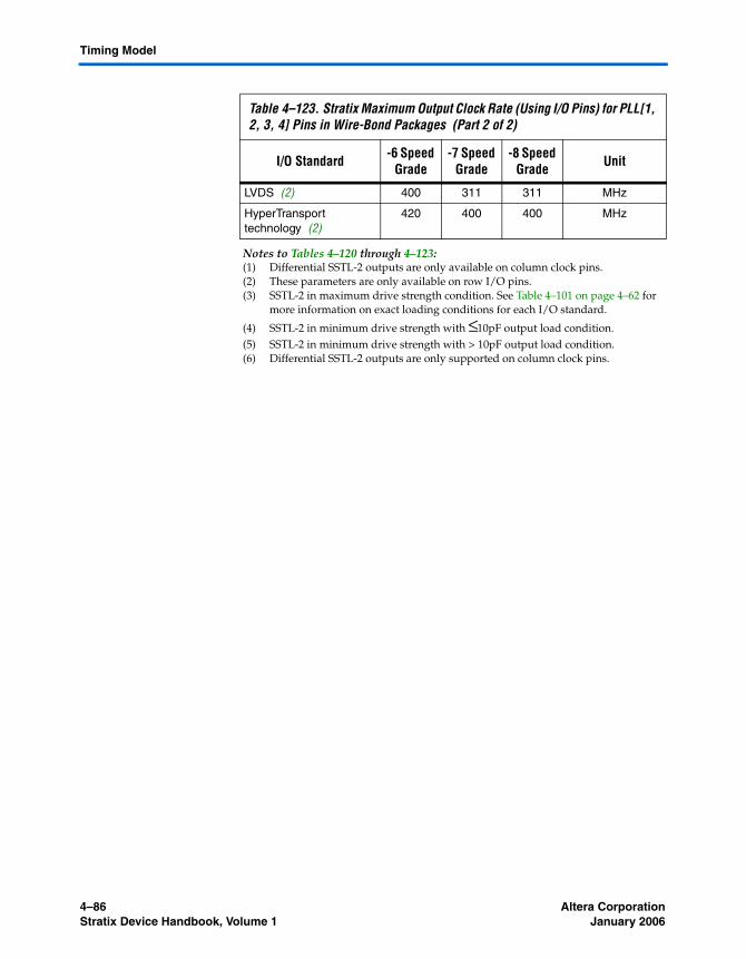
4–86 Altera CorporationStratix Device Handbook, Volume 1 January 2006
Timing Model
LVDS (2) 400 311 311 MHz
HyperTransport technology (2)
420 400 400 MHz
Notes to Tables 4–120 through 4–123:(1) Differential SSTL-2 outputs are only available on column clock pins.(2) These parameters are only available on row I/O pins.(3) SSTL-2 in maximum drive strength condition. See Table 4–101 on page 4–62 for
more information on exact loading conditions for each I/O standard.
(4) SSTL-2 in minimum drive strength with ≤ 10pF output load condition.(5) SSTL-2 in minimum drive strength with > 10pF output load condition.(6) Differential SSTL-2 outputs are only supported on column clock pins.
Table 4–123. Stratix Maximum Output Clock Rate (Using I/O Pins) for PLL[1, 2, 3, 4] Pins in Wire-Bond Packages (Part 2 of 2)
I/O Standard -6 Speed Grade
-7 Speed Grade
-8 Speed Grade Unit

Altera Corporation 4–87January 2006 Stratix Device Handbook, Volume 1
DC & Switching Characteristics
High-Speed I/O Specification
Table 4–124 provides high-speed timing specifications definitions.
Table 4–124. High-Speed Timing Specifications & Terminology
High-Speed Timing Specification Terminology
tC High-speed receiver/transmitter input and output clock period.
fHSCLK High-speed receiver/transmitter input and output clock frequency.
tRISE Low-to-high transmission time.
tFALL High-to-low transmission time.
Timing unit interval (TUI) The timing budget allowed for skew, propagation delays, and data sampling window. (TUI = 1/(Receiver Input Clock Frequency × Multiplication Factor) = tC/w).
fHSDR Maximum LVDS data transfer rate (fHSDR = 1/TUI).
Channel-to-channel skew (TCCS) The timing difference between the fastest and slowest output edges, including tCO variation and clock skew. The clock is included in the TCCS measurement.
Sampling window (SW) The period of time during which the data must be valid to be captured correctly. The setup and hold times determine the ideal strobe position within the sampling window.SW = tSW (max) – tSW (min).
Input jitter (peak-to-peak) Peak-to-peak input jitter on high-speed PLLs.
Output jitter (peak-to-peak) Peak-to-peak output jitter on high-speed PLLs.
tDUTY Duty cycle on high-speed transmitter output clock.
tLOCK Lock time for high-speed transmitter and receiver PLLs.
J Deserialization factor (width of internal data bus).
W PLL multiplication factor.

4–88
Altera C
orp
oratio
nS
tratix Device H
and
bo
ok, Vo
lum
e 1
Janu
ary 2006
Hig
h-S
peed
I/O S
pecificatio
n
Tables 4–125 and 4–126 show the high-speed I/O timing for Stratix devices.
Table 4–125. High-Speed I/O Specifications for Flip-Chip Packages (Part 1 of 4) Notes (1), (2)
Symbol Conditions-5 Speed Grade -6 Speed Grade -7 Speed Grade -8 Speed Grade
UnitMin Typ Max Min Typ Max Min Typ Max Min Typ Max
fHSCLK (Clock frequency)(LVDS, LVPECL, HyperTransport technology)fHSCLK = fHSDR / W
W = 4 to 30 (Serdes used)
10 210 10 210 10 156 10 115.5 MHz
W = 2 (Serdes bypass)
50 231 50 231 50 231 50 231 MHz
W = 2 (Serdes used)
150 420 150 420 150 312 150 231 MHz
W = 1 (Serdes bypass)
100 462 100 462 100 462 100 462 MHz
W = 1 (Serdes used)
300 717 300 717 300 624 300 462 MHz
fHSDR Device operation(LVDS, LVPECL, HyperTransport technology)
J = 10 300 840 300 840 300 640 300 462 Mbps
J = 8 300 840 300 840 300 640 300 462 Mbps
J = 7 300 840 300 840 300 640 300 462 Mbps
J = 4 300 840 300 840 300 640 300 462 Mbps
J = 2 100 462 100 462 100 640 100 462 Mbps
J = 1 (LVDS and LVPECL only)
100 462 100 462 100 640 100 462 Mbps
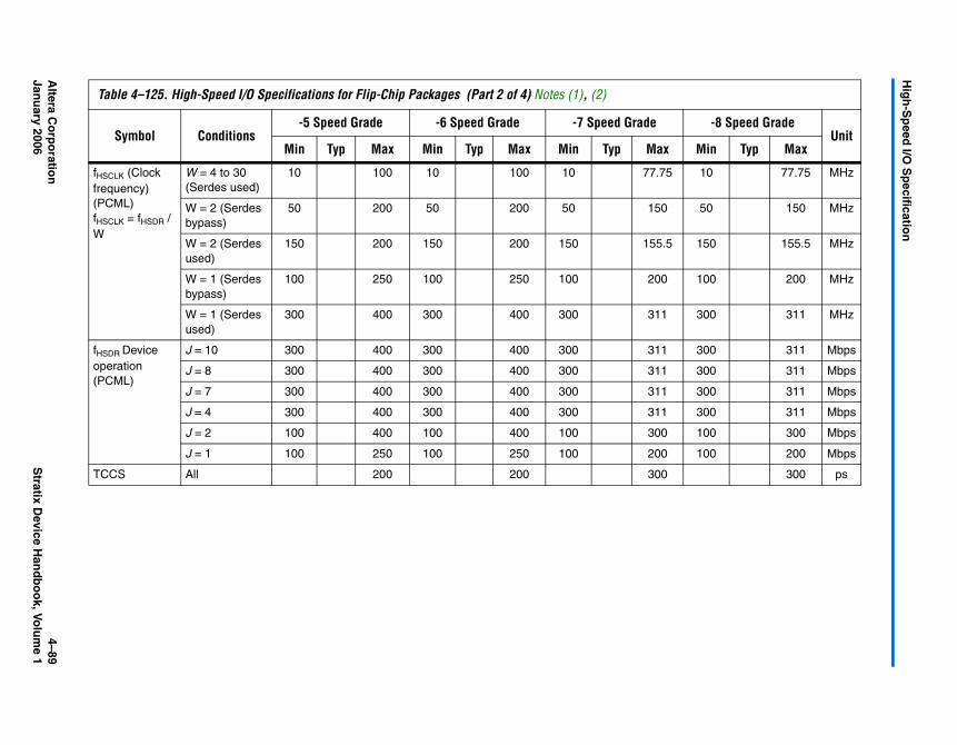
Altera C
orp
oratio
n
4–89
Janu
ary 2006
Stratix D
evice Han
db
oo
k, Volu
me 1
Hig
h-S
peed
I/O S
pecificatio
n
fHSCLK (Clock frequency)(PCML)fHSCLK = fHSDR / W
W = 4 to 30 (Serdes used)
10 100 10 100 10 77.75 10 77.75 MHz
W = 2 (Serdes bypass)
50 200 50 200 50 150 50 150 MHz
W = 2 (Serdes used)
150 200 150 200 150 155.5 150 155.5 MHz
W = 1 (Serdes bypass)
100 250 100 250 100 200 100 200 MHz
W = 1 (Serdes used)
300 400 300 400 300 311 300 311 MHz
fHSDR Device operation (PCML)
J = 10 300 400 300 400 300 311 300 311 Mbps
J = 8 300 400 300 400 300 311 300 311 Mbps
J = 7 300 400 300 400 300 311 300 311 Mbps
J = 4 300 400 300 400 300 311 300 311 Mbps
J = 2 100 400 100 400 100 300 100 300 Mbps
J = 1 100 250 100 250 100 200 100 200 Mbps
TCCS All 200 200 300 300 ps
Table 4–125. High-Speed I/O Specifications for Flip-Chip Packages (Part 2 of 4) Notes (1), (2)
Symbol Conditions-5 Speed Grade -6 Speed Grade -7 Speed Grade -8 Speed Grade
UnitMin Typ Max Min Typ Max Min Typ Max Min Typ Max
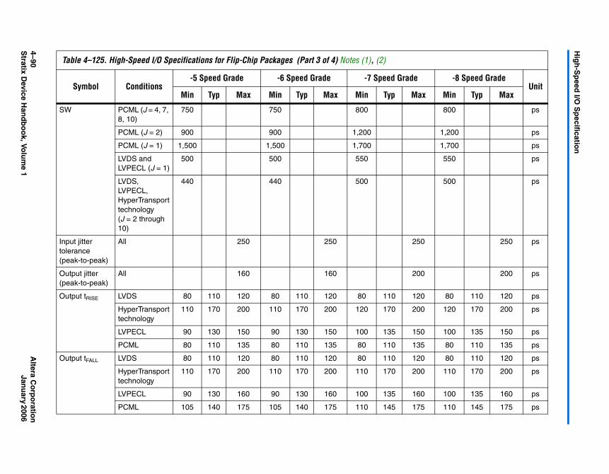
4–90
Altera C
orp
oratio
nS
tratix Device H
and
bo
ok, Vo
lum
e 1
Janu
ary 2006
Hig
h-S
peed
I/O S
pecificatio
n
SW PCML (J = 4, 7, 8, 10)
750 750 800 800 ps
PCML (J = 2) 900 900 1,200 1,200 ps
PCML (J = 1) 1,500 1,500 1,700 1,700 ps
LVDS and LVPECL (J = 1)
500 500 550 550 ps
LVDS, LVPECL, HyperTransport technology (J = 2 through 10)
440 440 500 500 ps
Input jitter tolerance (peak-to-peak)
All 250 250 250 250 ps
Output jitter (peak-to-peak)
All 160 160 200 200 ps
Output tRISE LVDS 80 110 120 80 110 120 80 110 120 80 110 120 ps
HyperTransport technology
110 170 200 110 170 200 120 170 200 120 170 200 ps
LVPECL 90 130 150 90 130 150 100 135 150 100 135 150 ps
PCML 80 110 135 80 110 135 80 110 135 80 110 135 ps
Output tFALL LVDS 80 110 120 80 110 120 80 110 120 80 110 120 ps
HyperTransport technology
110 170 200 110 170 200 110 170 200 110 170 200 ps
LVPECL 90 130 160 90 130 160 100 135 160 100 135 160 ps
PCML 105 140 175 105 140 175 110 145 175 110 145 175 ps
Table 4–125. High-Speed I/O Specifications for Flip-Chip Packages (Part 3 of 4) Notes (1), (2)
Symbol Conditions-5 Speed Grade -6 Speed Grade -7 Speed Grade -8 Speed Grade
UnitMin Typ Max Min Typ Max Min Typ Max Min Typ Max

Altera C
orp
oratio
n
4–91
Janu
ary 2006
Stratix D
evice Han
db
oo
k, Volu
me 1
Hig
h-S
peed
I/O S
pecificatio
n
tDUTY LVDS (J = 2 through 10)
47.5 50 52.5 47.5 50 52.5 47.5 50 52.5 47.5 50 52.5 %
LVDS (J =1) and LVPECL, PCML, HyperTransport technology
45 50 55 45 50 55 45 50 55 45 50 55 %
tLOCK All 100 100 100 100 μs
Notes to Table 4–125:(1) When J = 4, 7, 8, and 10, the SERDES block is used.(2) When J = 2 or J = 1, the SERDES is bypassed.
Table 4–125. High-Speed I/O Specifications for Flip-Chip Packages (Part 4 of 4) Notes (1), (2)
Symbol Conditions-5 Speed Grade -6 Speed Grade -7 Speed Grade -8 Speed Grade
UnitMin Typ Max Min Typ Max Min Typ Max Min Typ Max

4–92
Altera C
orp
oratio
nS
tratix Device H
and
bo
ok, Vo
lum
e 1
Janu
ary 2006
Hig
h-S
peed
I/O S
pecificatio
n
Table 4–126. High-Speed I/O Specifications for Wire-Bond Packages (Part 1 of 2)
Symbol Conditions-6 Speed Grade -7 Speed Grade -8 Speed Grade
UnitMin Typ Max Min Typ Max Min Typ Max
fHSCLK (Clock frequency)(LVDS,LVPECL, HyperTransport technology)fHSCLK = fHSDR / W
W = 4 to 30 (Serdes used) 10 156 10 115.5 10 115.5 MHz
W = 2 (Serdes bypass) 50 231 50 231 50 231 MHz
W = 2 (Serdes used) 150 312 150 231 150 231 MHz
W = 1 (Serdes bypass) 100 311 100 270 100 270 MHz
W = 1 (Serdes used) 300 624 300 462 300 462 MHz
fHSDR Device operation, (LVDS,LVPECL, HyperTransport technology)
J = 10 300 624 300 462 300 462 Mbps
J = 8 300 624 300 462 300 462 Mbps
J = 7 300 624 300 462 300 462 Mbps
J = 4 300 624 300 462 300 462 Mbps
J = 2 100 462 100 462 100 462 Mbps
J = 1 (LVDS and LVPECL only)
100 311 100 270 100 270 Mbps
fH S C L K (Clock frequency)(PCML)fHSCLK = fHSDR / W
W = 4 to 30 (Serdes used) 10 77.75 MHz
W = 2 (Serdes bypass) 50 150 50 77.5 50 77.5 MHz
W = 2 (Serdes used) 150 155.5 MHz
W = 1 (Serdes bypass) 100 200 100 155 100 155 MHz
W = 1 (Serdes used) 300 311 MHz
Device operation, fH S D R
(PCML)
J = 10 300 311 Mbps
J = 8 300 311 Mbps
J = 7 300 311 Mbps
J = 4 300 311 Mbps
J = 2 100 300 100 155 100 155 Mbps
J = 1 100 200 100 155 100 155 Mbps
TCCS All 400 400 400 ps

Altera C
orp
oratio
n
4–93
Janu
ary 2006
Stratix D
evice Han
db
oo
k, Volu
me 1
Hig
h-S
peed
I/O S
pecificatio
n
SW PCML (J = 4, 7, 8, 10) only 800 800 800 ps
PCML (J = 2) only 1,200 1,200 1,200 ps
PCML (J = 1) only 1,700 1,700 1,700 ps
LVDS and LVPECL (J = 1) only
550 550 550 ps
LVDS, LVPECL, HyperTransport technology (J = 2 through 10) only
500 500 500 ps
Input jitter tolerance (peak-to-peak)
All 250 250 250 ps
Output jitter (peak-to-peak)
All 200 200 200 ps
Output tR I S E LVDS 80 110 120 80 110 120 80 110 120 ps
HyperTransport technology 120 170 200 120 170 200 120 170 200 ps
LVPECL 100 135 150 100 135 150 100 135 150 ps
PCML 80 110 135 80 110 135 80 110 135 ps
Output tFA L L LVDS 80 110 120 80 110 120 80 110 120 ps
HyperTransport 110 170 200 110 170 200 110 170 200 ps
LVPECL 100 135 160 100 135 160 100 135 160 ps
PCML 110 145 175 110 145 175 110 145 175 ps
tD UT Y LVDS (J = 2 through10) only 47.5 50 52.5 47.5 50 52.5 47.5 50 52.5 %
LVDS (J =1) and LVPECL, PCML, HyperTransport technology
45 50 55 45 50 55 45 50 55 %
tL O C K All 100 100 100 μs
Table 4–126. High-Speed I/O Specifications for Wire-Bond Packages (Part 2 of 2)
Symbol Conditions-6 Speed Grade -7 Speed Grade -8 Speed Grade
UnitMin Typ Max Min Typ Max Min Typ Max

4–94 Altera CorporationStratix Device Handbook, Volume 1 January 2006
PLL Specifications
PLL Specifications
Tables 4–127 through 4–129 describe the Stratix device enhanced PLL specifications.
Table 4–127. Enhanced PLL Specifications for -5 Speed Grades (Part 1 of 2)
Symbol Parameter Min Typ Max Unit
fIN Input clock frequency 3(1), (2)
684 MHz
fINPFD Input frequency to PFD 3 420 MHz
fINDUTY Input clock duty cycle 40 60 %
fEINDUTY External feedback clock input duty cycle
40 60 %
tINJITTER Input clock period jitter ±200 (3) ps
tEINJITTER External feedback clock period jitter ±200 (3) ps
tFCOMP External feedback clock compensation time (4)
6 ns
fOUT Output frequency for internal global or regional clock
0.3 500 MHz
fOUT_EXT Output frequency for external clock (3)
0.3 526 MHz
tOUTDUTY Duty cycle for external clock output (when set to 50%)
45 55 %
tJITTER Period jitter for external clock output (6)
±100 ps for >200-MHz outclk±20 mUI for <200-MHz outclk
ps or mUI
tCONFIG5,6 Time required to reconfigure the scan chains for PLLs 5 and 6
289/fSCANCLK
tCONFIG11,12 Time required to reconfigure the scan chains for PLLs 11 and 12
193/fSCANCLK
tSCANCLK scanclk frequency (5) 22 MHz
tDLOCK Time required to lock dynamically (after switchover or reconfiguring any non-post-scale counters/delays) (7)
100 μs
tLOCK Time required to lock from end of device configuration
10 400 μs
fVCO PLL internal VCO operating range 300 800 (8) MHz
tLSKEW Clock skew between two external clock outputs driven by the same counter
±50 ps

Altera Corporation 4–95January 2006 Stratix Device Handbook, Volume 1
DC & Switching Characteristics
tSKEW Clock skew between two external clock outputs driven by the different counters with the same settings
±75 ps
fSS Spread spectrum modulation frequency
30 150 kHz
% spread Percentage spread for spread spectrum frequency (10)
0.4 0.5 0.6 %
tARESET Minimum pulse width on areset signal
10 ns
tA R E S E T _ RE C O NF I G
Minimum pulse width on the areset signal when using PLL reconfiguration. Reset the PLL after scandataout goes high.
500 ns
Table 4–128. Enhanced PLL Specifications for -6 Speed Grades (Part 1 of 2)
Symbol Parameter Min Typ Max Unit
fIN Input clock frequency 3(1), (2)
650 MHz
fINPFD Input frequency to PFD 3 420 MHz
fINDUTY Input clock duty cycle 40 60 %
fEINDUTY External feedback clock input duty cycle
40 60 %
tINJITTER Input clock period jitter ±200 (3) ps
tEINJITTER External feedback clock period jitter ±200 (3) ps
tFCOMP External feedback clock compensation time (4)
6 ns
fOUT Output frequency for internal global or regional clock
0.3 450 MHz
fOUT_EXT Output frequency for external clock (3) 0.3 500 MHz
tOUTDUTY Duty cycle for external clock output (when set to 50%)
45 55 %
tJITTER Period jitter for external clock output (6)
±100 ps for >200-MHz outclk±20 mUI for <200-MHz outclk
ps or mUI
tCONFIG5,6 Time required to reconfigure the scan chains for PLLs 5 and 6
289/fSCANCLK
tCONFIG11,12 Time required to reconfigure the scan chains for PLLs 11 and 12
193/fSCANCLK
Table 4–127. Enhanced PLL Specifications for -5 Speed Grades (Part 2 of 2)
Symbol Parameter Min Typ Max Unit

4–96 Altera CorporationStratix Device Handbook, Volume 1 January 2006
PLL Specifications
tSCANCLK scanclk frequency (5) 22 MHz
tDLOCK Time required to lock dynamically (after switchover or reconfiguring any non-post-scale counters/delays) (7) (11)
(9) 100 μs
tLOCK Time required to lock from end of device configuration (11)
10 400 μs
fVCO PLL internal VCO operating range 300 800 (8) MHz
tLSKEW Clock skew between two external clock outputs driven by the same counter
±50 ps
tSKEW Clock skew between two external clock outputs driven by the different counters with the same settings
±75 ps
fSS Spread spectrum modulation frequency
30 150 kHz
% spread Percentage spread for spread spectrum frequency (10)
0.4 0.5 0.6 %
tARESET Minimum pulse width on areset signal
10 ns
Table 4–129. Enhanced PLL Specifications for -7 Speed Grade (Part 1 of 2)
Symbol Parameter Min Typ Max Unit
fIN Input clock frequency 3 (1), (2)
565 MHz
fINPFD Input frequency to PFD 3 420 MHz
fINDUTY Input clock duty cycle 40 60 %
fEINDUTY External feedback clock input duty cycle
40 60 %
tINJITTER Input clock period jitter ±200 (3) ps
tEINJITTER External feedback clock period jitter ±200 (3) ps
tFCOMP External feedback clock compensation time (4)
6 ns
fOUT Output frequency for internal global or regional clock
0.3 420 MHz
fOUT_EXT Output frequency for external clock (3)
0.3 434 MHz
Table 4–128. Enhanced PLL Specifications for -6 Speed Grades (Part 2 of 2)
Symbol Parameter Min Typ Max Unit
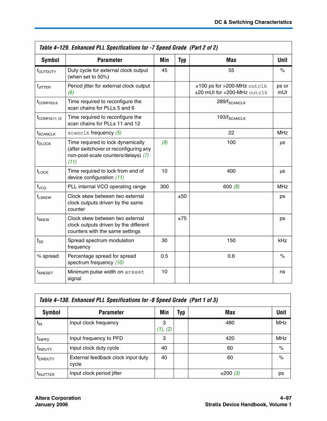
Altera Corporation 4–97January 2006 Stratix Device Handbook, Volume 1
DC & Switching Characteristics
tOUTDUTY Duty cycle for external clock output (when set to 50%)
45 55 %
tJITTER Period jitter for external clock output (6)
±100 ps for >200-MHz outclk±20 mUI for <200-MHz outclk
ps or mUI
tCONFIG5,6 Time required to reconfigure the scan chains for PLLs 5 and 6
289/fSCANCLK
tCONFIG11,12 Time required to reconfigure the scan chains for PLLs 11 and 12
193/fSCANCLK
tSCANCLK scanclk frequency (5) 22 MHz
tDLOCK Time required to lock dynamically (after switchover or reconfiguring any non-post-scale counters/delays) (7) (11)
(9) 100 μs
tLOCK Time required to lock from end of device configuration (11)
10 400 μs
fVCO PLL internal VCO operating range 300 600 (8) MHz
tLSKEW Clock skew between two external clock outputs driven by the same counter
±50 ps
tSKEW Clock skew between two external clock outputs driven by the different counters with the same settings
±75 ps
fSS Spread spectrum modulation frequency
30 150 kHz
% spread Percentage spread for spread spectrum frequency (10)
0.5 0.6 %
tARESET Minimum pulse width on areset signal
10 ns
Table 4–130. Enhanced PLL Specifications for -8 Speed Grade (Part 1 of 3)
Symbol Parameter Min Typ Max Unit
fIN Input clock frequency 3(1), (2)
480 MHz
fINPFD Input frequency to PFD 3 420 MHz
fINDUTY Input clock duty cycle 40 60 %
fEINDUTY External feedback clock input duty cycle
40 60 %
tINJITTER Input clock period jitter ±200 (3) ps
Table 4–129. Enhanced PLL Specifications for -7 Speed Grade (Part 2 of 2)
Symbol Parameter Min Typ Max Unit

4–98 Altera CorporationStratix Device Handbook, Volume 1 January 2006
PLL Specifications
tEINJITTER External feedback clock period jitter ±200 (3) ps
tFCOMP External feedback clock compensation time (4)
6 ns
fOUT Output frequency for internal global or regional clock
0.3 357 MHz
fOUT_EXT Output frequency for external clock (3)
0.3 369 MHz
tOUTDUTY Duty cycle for external clock output (when set to 50%)
45 55 %
tJITTER Period jitter for external clock output (6)
±100 ps for >200-MHz outclk±20 mUI for <200-MHz outclk
ps or mUI
tCONFIG5,6 Time required to reconfigure the scan chains for PLLs 5 and 6
289/fSCANCLK
tCONFIG11,12 Time required to reconfigure the scan chains for PLLs 11 and 12
193/fSCANCLK
tSCANCLK scanclk frequency (5) 22 MHz
tDLOCK Time required to lock dynamically (after switchover or reconfiguring any non-post-scale counters/delays) (7) (11)
(9) 100 μs
tLOCK Time required to lock from end of device configuration (11)
10 400 μs
fVCO PLL internal VCO operating range 300 600 (8) MHz
Table 4–130. Enhanced PLL Specifications for -8 Speed Grade (Part 2 of 3)
Symbol Parameter Min Typ Max Unit
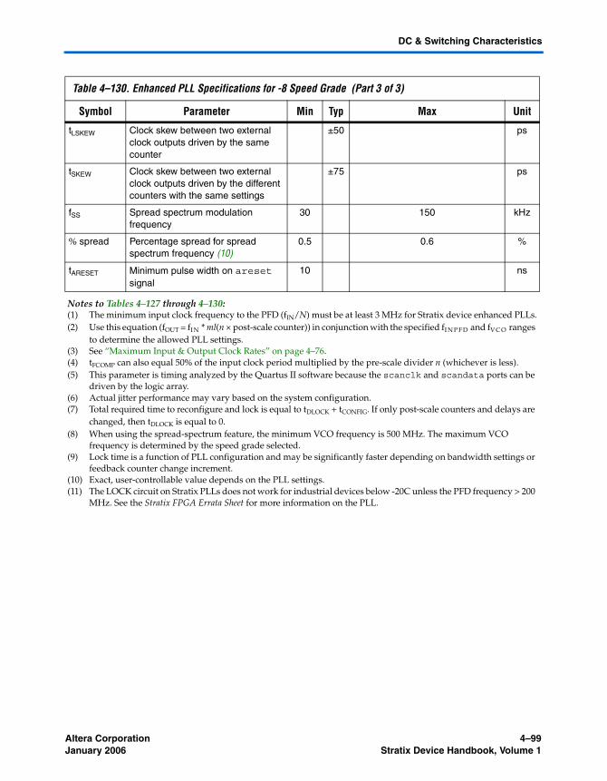
Altera Corporation 4–99January 2006 Stratix Device Handbook, Volume 1
DC & Switching Characteristics
tLSKEW Clock skew between two external clock outputs driven by the same counter
±50 ps
tSKEW Clock skew between two external clock outputs driven by the different counters with the same settings
±75 ps
fSS Spread spectrum modulation frequency
30 150 kHz
% spread Percentage spread for spread spectrum frequency (10)
0.5 0.6 %
tARESET Minimum pulse width on areset signal
10 ns
Notes to Tables 4–127 through 4–130:(1) The minimum input clock frequency to the PFD (fIN/N) must be at least 3 MHz for Stratix device enhanced PLLs.(2) Use this equation (fOUT = fI N * ml(n × post-scale counter)) in conjunction with the specified fI N P F D and fV C O ranges
to determine the allowed PLL settings.(3) See “Maximum Input & Output Clock Rates” on page 4–76.(4) tFCOMP can also equal 50% of the input clock period multiplied by the pre-scale divider n (whichever is less).(5) This parameter is timing analyzed by the Quartus II software because the scanclk and scandata ports can be
driven by the logic array.(6) Actual jitter performance may vary based on the system configuration.(7) Total required time to reconfigure and lock is equal to tDLOCK + tCONFIG. If only post-scale counters and delays are
changed, then tDLOCK is equal to 0.(8) When using the spread-spectrum feature, the minimum VCO frequency is 500 MHz. The maximum VCO
frequency is determined by the speed grade selected.(9) Lock time is a function of PLL configuration and may be significantly faster depending on bandwidth settings or
feedback counter change increment.(10) Exact, user-controllable value depends on the PLL settings.(11) The LOCK circuit on Stratix PLLs does not work for industrial devices below -20C unless the PFD frequency > 200
MHz. See the Stratix FPGA Errata Sheet for more information on the PLL.
Table 4–130. Enhanced PLL Specifications for -8 Speed Grade (Part 3 of 3)
Symbol Parameter Min Typ Max Unit

4–100 Altera CorporationStratix Device Handbook, Volume 1 January 2006
PLL Specifications
Tables 4–131 through 4–133 describe the Stratix device fast PLL specifications.
Table 4–131. Fast PLL Specifications for -5 & -6 Speed Grade Devices
Symbol Parameter Min Max Unit
fIN CLKIN frequency (1), (2), (3) 10 717 MHz
fINPFD Input frequency to PFD 10 500 MHz
fOUT Output frequency for internal global or regional clock (3)
9.375 420 MHz
fOUT_DIFFIO Output frequency for external clock driven out on a differential I/O data channel (2)
(5) (5)
fVCO VCO operating frequency 300 1,000 MHz
tINDUTY CLKIN duty cycle 40 60 %
tINJITTER Period jitter for CLKIN pin ±200 ps
tDUTY Duty cycle for DFFIO 1× CLKOUT pin (6) 45 55 %
tJITTER Period jitter for DIFFIO clock out (6) (5) ps
tLOCK Time required for PLL to acquire lock 10 100 μs
m Multiplication factors for m counter (6) 1 32 Integer
l0, l1, g0 Multiplication factors for l0, l1, and g0 counter (7), (8)
1 32 Integer
tARESET Minimum pulse width on areset signal
10 ns
Table 4–132. Fast PLL Specifications for -7 Speed Grades (Part 1 of 2)
Symbol Parameter Min Max Unit
fIN CLKIN frequency (1), (3) 10 640 MHz
fINPFD Input frequency to PFD 10 500 MHz
fOUT Output frequency for internal global or regional clock (4)
9.375 420 MHz
fOUT_DIFFIO Output frequency for external clock driven out on a differential I/O data channel
(5) (5) MHz
fVCO VCO operating frequency 300 700 MHz
tINDUTY CLKIN duty cycle 40 60 %
tINJITTER Period jitter for CLKIN pin ±200 ps
tDUTY Duty cycle for DFFIO 1× CLKOUT pin (6) 45 55 %

Altera Corporation 4–101January 2006 Stratix Device Handbook, Volume 1
DC & Switching Characteristics
tJITTER Period jitter for DIFFIO clock out (6) (5) ps
tLOCK Time required for PLL to acquire lock 10 100 μs
m Multiplication factors for m counter (7) 1 32 Integer
l0, l1, g0 Multiplication factors for l0, l1, and g0 counter (7), (8)
1 32 Integer
tARESET Minimum pulse width on areset signal
10 ns
Table 4–133. Fast PLL Specifications for -8 Speed Grades (Part 1 of 2)
Symbol Parameter Min Max Unit
fIN CLKIN frequency (1), (3) 10 460 MHz
fINPFD Input frequency to PFD 10 500 MHz
fOUT Output frequency for internal global or regional clock (4)
9.375 420 MHz
fOUT_DIFFIO Output frequency for external clock driven out on a differential I/O data channel
(5) (5) MHz
fVCO VCO operating frequency 300 700 MHz
tINDUTY CLKIN duty cycle 40 60 %
tINJITTER Period jitter for CLKIN pin ±200 ps
tDUTY Duty cycle for DFFIO 1× CLKOUT pin (6) 45 55 %
tJITTER Period jitter for DIFFIO clock out (6) (5) ps
tLOCK Time required for PLL to acquire lock 10 100 μs
m Multiplication factors for m counter (7) 1 32 Integer
l0, l1, g0 Multiplication factors for l0, l1, and g0 counter (7), (8)
1 32 Integer
Table 4–132. Fast PLL Specifications for -7 Speed Grades (Part 2 of 2)
Symbol Parameter Min Max Unit

4–102 Altera CorporationStratix Device Handbook, Volume 1 January 2006
DLL Specifications
DLL Specifications
Table 4–134 reports the jitter for the DLL in the DQS phase shift reference circuit.
f For more information on DLL jitter, see the DDR SRAM section in the Stratix Architecture chapter of the Stratix Device Handbook, Volume 1.
Table 4–135 lists the Stratix DLL low frequency limit for full phase shift across all PVT conditions. The Stratix DLL can be used below these frequencies, but it will not achieve the full phase shift requested across all
tARESET Minimum pulse width on areset signal
10 ns
Notes to Tables 4–131 through 4–133:(1) See “Maximum Input & Output Clock Rates” on page 4–76.(2) PLLs 7, 8, 9, and 10 in the EP1S80 device support up to 717-MHz input and output.
(3) Use this equation (fO U T = fI N * ml(n × post-scale counter)) in conjunction with the specified fI N P F D and fV C O ranges to determine the allowed PLL settings.
(4) When using the SERDES, high-speed differential I/O mode supports a maximum output frequency of 210 MHz to the global or regional clocks (that is, the maximum data rate 840 Mbps divided by the smallest SERDES J factor of 4).
(5) Refer to the section “High-Speed I/O Specification” on page 4–87 for more information.(6) This parameter is for high-speed differential I/O mode only.(7) These counters have a maximum of 32 if programmed for 50/50 duty cycle. Otherwise, they have a maximum
of 16. (8) High-speed differential I/O mode supports W = 1 to 16 and J = 4, 7, 8, or 10.
Table 4–133. Fast PLL Specifications for -8 Speed Grades (Part 2 of 2)
Symbol Parameter Min Max Unit
Table 4–134. DLL Jitter for DQS Phase Shift Reference Circuit
Frequency (MHz) DLL Jitter (ps)
197 to 200 ± 100
160 to 196 ± 300
100 to 159 ± 500

Altera Corporation 4–103January 2006 Stratix Device Handbook, Volume 1
DC & Switching Characteristics
process and operating conditions. Run the timing analyzer in the Quartus II software at the fast and slow operating conditions to see the phase shift range that is achieved below these frequencies.
Table 4–135. Stratix DLL Low Frequency Limit for Full Phase Shift
Phase Shift Minimum Frequency for Full Phase Shift Unit
72° 119 MHz
90° 149 MHz

4–104 Altera CorporationStratix Device Handbook, Volume 1 January 2006
DLL Specifications

Altera Corporation 5–1September 2004
5. Reference & OrderingInformation
Software Stratix® devices are supported by the Altera® Quartus® II design software, which provides a comprehensive environment for system-on-a-programmable-chip (SOPC) design. The Quartus II software includes HDL and schematic design entry, compilation and logic synthesis, full simulation and advanced timing analysis, SignalTap® II logic analyzer, and device configuration. See the Design Software Selector Guide for more details on the Quartus II software features.
The Quartus II software supports the Windows XP/2000/NT/98, Sun Solaris, Linux Red Hat v7.1 and HP-UX operating systems. It also supports seamless integration with industry-leading EDA tools through the NativeLink® interface.
Device Pin-Outs Stratix device pin-outs can be found on the Altera web site (www.altera.com).
Ordering Information
Figure 5–1 describes the ordering codes for Stratix devices. For more information on a specific package, see the Package Information for Stratix Devices chapter.
S51005-2.1
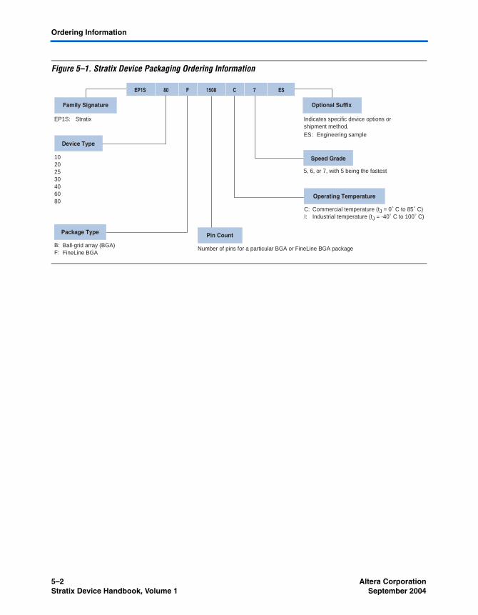
5–2 Altera CorporationStratix Device Handbook, Volume 1 September 2004
Ordering Information
Figure 5–1. Stratix Device Packaging Ordering Information
Device Type
Package Type
5, 6, or 7, with 5 being the fastest
Number of pins for a particular BGA or FineLine BGA package
ES:
B:F:
Ball-grid array (BGA)FineLine BGA
EP1S: Stratix
10202530406080
C:I:
Commercial temperature (tJ = 0˚ C to 85˚ C)Industrial temperature (tJ = -40˚ C to 100˚ C)
Optional SuffixFamily Signature
Operating Temperature
Speed Grade
Pin Count
Engineering sample
7EP1S 80 C1508F ES
Indicates specific device options or shipment method.

Altera Corporation Index–1
Index
AAccumulator 2–63Adder/Output Blocks 2–61Adder/Subtractor
2–63Accumulator
2–63AGP 1x Specifications 4–13AGP 2x Specifications 4–13Architecture 2–1
36 x 36 Multiply Mode 2–66addnsub Signal 2–8Block Diagram 2–2Bus Hold 2–121Byte Alignment 2–140Carry-Select Chain 2–11Clear & Preset Logic Control 2–13Combined Resources 2–78Dedicated Circuitry 2–137Device Resources 2–3Device Routing Scheme 2–20Digital Signal Processing Block 2–52Direct Link Connection 2–5Dynamic Arithmetic Mode 2–10
in LE 2–11Four-Multipliers
Adder Mode 2–68Functional Description 2–1LAB
Interconnects 2–4Logic Array Blocks 2–3Structure 2–4
LE Operating Modes 2–8Logic Elements 2–6Modes of Operation 2–64Multiplier Size & Configurations per DSP
block 2–70Multiply-Accumulator Mode 2–67MultiTrack Interconnect 2–14Normal Mode 2–9
in LE 2–9
Open-Drain Output 2–120Power Sequencing & Hot Socketing 2–140Programmable Drive Strength 2–119Programmable Pull-Up Resistor 2–122Simple Multiplier Mode 2–64Single-Port Mode 2–51Slew-Rate Control 2–120Two-Multipliers
Adder Mode 2–67Adder Mode Implementing Complex
Multiply 2–68
CClass I Specifications 4–11, 4–12Class II Specifications 4–11, 4–12, 4–13Clocks
Clock Feedback 2–96Clock Multiplication & Division 2–88, 2–101Clock Switchover
2–88Delay 2–97EP1S10, EP1S20 & EP1S25
Device I/O Clock Groups2–80
EP1S25, EP1S20 & EP1S10 Device Fast ClockPin Connections to Fast RegionalClocks 2–77
EP1S30 Device Fast Regional Clock Pin Con-nections to Fast Regional Clocks 2–78
EP1S30, EP1S40, EP1S60, EP1S80Device I/O Clock Groups
2–81External Clock
Inputs 2–102Outputs 2–92, 2–103Outputs for Enhanced PLLs 11 & 12 2–95Outputs for PLLs 5 & 6 2–93
Fast Regional Clock External I/O TimingParameters 4–34
Fast Regional Clock Network 2–76

Index–2 Altera Corporation
Stratix Device Handbook, Volume 1
Global & Hierarchical Clocking 2–73Global & Regional Clock Connections
from Side Pins & Fast PLL Outputs 2–85from Top Clock Pins & Enhanced PLL
Outputs 2–86Global Clock External I/O Timing
Parameters 4–35Global Clock Network 2–74Global Clocking 2–75Independent Clock Mode 2–44Input/Output
Clock Mode2–46
Simple Dual-Port Mode 2–48True Dual-Port Mode 2–47
Maximum Input & Output Clock Rates 4–76Maximum Input Clock Rate
for CLK(0, 2, 9, 11) Pins inFlip-Chip
Packages 4–77
Wire-BondPackages 4–79
(1, 3, 8, 10) Pins inFlip-Chip
Packages 4–78
Wire-BondPackages 4–80
(7..4) & CLK(15..12) Pins inFlip-Chip
Packages 4–76
Wire-BondPackages 4–78
Maximum Output Clock Ratefor PLL
(1, 2, 3, 4) Pins inFlip-Chip
Packages 4–83
Wire-BondPackages 4–85
(5, 6, 11, 12) Pins inFlip-Chip
Packages 4–81
Wire-BondPackages 4–84
Phase & Delay Shifting 2–96Phase Delay 2–96PLL Clock Networks 2–73Read/Write Clock Mode
2–49in Simple Dual-Port Mode 2–50
Regional Clock 2–75External I/O Timing Parameters 4–34
Regional Clock Bus 2–79Regional Clock Network 2–75Spread-Spectrum Clocking 2–98
Configuration 3–532-Bit IDCODE 3–3and Testing 3–1Data Sources for Configuration 3–7Local Update Mode 3–12Local Update Transition Diagram 3–12Operating Modes 3–5Partial Reconfiguration 3–7Remote Update 3–8Remote Update Transition Diagram 3–11Schemes 3–7SignalTap II Embedded Logic Analyzer 3–5Stratix FPGAs with JRunner 3–7
Control Signals 2–104
DDC Switching
Absolute Maximum Ratings 4–1Bus Hold Parameters 4–16Capacitance 4–17DC & Switching Characteristics 4–1External Timing Parameters 4–33Operating Conditions 4–1Performance 4–20Power Consumption 4–17Recommended Operating Conditions 4–1
DDRDouble-Data Rate I/O Pins 2–111
Device FeaturesEP1S10, EP1S20, EP1S25, EP1S30, 1–3EP1S40, EP1S60, EP1S80, 1–3

Altera Corporation Index–3
Stratix Device Handbook, Volume 1
Differential HSTL Specifications 4–15DSP
Block DiagramConfiguration
for 18 x 18-Bit 2–55for 9 x 9-Bit 2–56
Block Interconnect Interface 2–71Block Interface 2–70Block Signal Sources & Destinations 2–73Blocks
Arranged in Columns 2–53in Stratix Devices 2–54
Input Register Modes 2–60Input Registers 2–58Multiplier
2–60Block 2–57Signed Representation 2–60Sub-Block 2–57Sub-Blocks Using Input Shift Register
Connections 2–59Pipeline/Post Multiply Register 2–61
EEP1S10 Devices
Column PinFast Regional Clock External I/O Timing
Parameters 4–36Global Clock External I/O Timing
Parameters 4–37Regional Clock External I/O Timing
Parameters 4–36Row Pin
Fast Regional Clock External I/O TimingParameters 4–37
Global Clock External I/O TimingParameters 4–38
Regional Clock External I/O TimingParameters 4–38
EP1S20 DevicesColumn Pin
Fast Regional Clock External I/O TimingParameters 4–39
Global Clock External I/O TimingParameters 4–40
Regional Clock External I/O Timing
Parameters 4–39Row Pin
Fast Regional Clock External I/O TimingParameters 4–40
Global Clock External I/O TimingParameters 4–41
Regional Clock External I/O TimingParameters 4–41
EP1S25 DevicesColumn Pin
Fast Regional Clock External I/O TimingParameters 4–42
Global Clock External I/O TimingParameters 4–43
Regional Clock External I/O TimingParameters 4–42
Row PinFast Regional Clock External I/O Timing
Parameters 4–43Global Clock External I/O Timing
Parameters 4–44Regional Clock External I/O Timing
Parameters 4–44EP1S30 Devices
Column PinFast Regional Clock External I/O Timing
Parameters 4–45Global Clock External I/O Timing
Parameters 4–45Regional Clock External I/O Timing
Parameters 4–45Row Pin
Fast Regional Clock External I/O TimingParameters 4–46
Global Clock External I/O TimingParameters 4–47
Regional Clock External I/O TimingParameters 4–47
EP1S40 DevicesColumn Pin
Fast Regional Clock External I/O TimingParameters 4–48
Global Clock External I/O TimingParameters 4–49
Regional Clock External I/O TimingParameters 4–48
Row Pin

Index–4 Altera Corporation
Stratix Device Handbook, Volume 1
Fast Regional Clock External I/O TimingParameters 4–49
Global Clock External I/O TimingParameters 4–50
Regional Clock External I/O TimingParameters 4–50
EP1S60 DevicesColumn Pin
Fast Regional Clock External I/O TimingParameters 4–51
Global Clock External I/O TimingParameters 4–52
Regional Clock External I/O TimingParameters 4–51
M-RAMInterface Locations 2–38
Row PinFast Regional Clock External I/O Timing
Parameters 4–52Global Clock External I/O Timing
Parameters 4–53Regional Clock External I/O Timing
Parameters 4–53EP1S80 Devices
Column PinFast Regional Clock External I/O Timing
Parameters 4–54Global Clock External I/O Timing
Parameters 4–55Regional Clock External I/O Timing
Parameters 4–54Global Clock External I/O Timing
Parameters 4–56Row Pin
Fast Regional Clock External I/O TimingParameters 4–55
Regional Clock External I/O TimingParameters 4–56
HHSTL
Class I Specifications 4–14, 4–15Class II Specifications 4–14, 4–15
II/O
Standards1.5-V 4–14, 4–15
I/O Specifications 4–41.8-V
I/O Specifications 4–42.5-V
I/O Specifications 4–33.3-V 4–13
LVDS I/O Specifications 4–6PCI Specifications 4–9PCML Specifications 4–8
Advanced I/O Standard Support 2–122Column I/O Block Connection to the
Interconnect 2–107Column Pin
Input Delay Adders 4–66Control Signal Selection per IOE 2–109CTT I/O Specifications 4–16Differential LVDS Input On-Chip
Termination 2–128External I/O Delay Parameters 4–66GTL+ I/O Specifications 4–10High-Speed Differential I/O
Support 2–130HyperTransport Technology
Specifications 4–9I/O Banks 2–125I/O Structure 2–104I/O Support by Bank 2–126IOE Structure 2–105LVCMOS Specifications 4–3LVDS Performance on Fast PLL
Input 2–103LVPECL Specifications 4–8LVTTL Specifications 4–3MultiVolt I/O Interface 2–129MultiVolt I/O Support 2–130Output Delay Adders for Fast Slew Rate
on Column Pins 4–68Output Delay Adders for Fast Slew Rate
on Row Pins 4–69Output Delay Adders for Slow Slew Rate
on Column Pins 4–70Package Options & I/O Pin Counts 1–4Receiver Input Waveforms for Differential

Altera Corporation Index–5
Stratix Device Handbook, Volume 1
I/O Standards 4–5Row I/O Block Connection to the
Interconnect 2–106Row Pin
Input Delay Adders 4–67Signal Path through the I/O Block 2–108SSTL-18 4–11SSTL-2 4–12SSTL-3 4–12, 4–13Stratix IOE in Bidirectional I/O
Configuration 2–110Supported I/O Standards 2–123Transmitter Output Waveforms for Differ-
ential I/O Standards 4–6Interconnect
C4 Connections 2–18DSP Block Interface to Interconnect 2–72Left-Facing M-RAM to Interconnect
Interface 2–40LUT Chain Register Chain
Interconnects 2–17M-RAM
Column Unit Interface toInterconnect 2–42
Row Unit Interface to Interconnect 2–41R4 Connections 2–15
IOEInternal Timing Microparameters 4–29
JJTAG
Boundary-ScanRegister Length 3–3Support 3–1
Stratix JTAGInstructions 3–2Waveforms 3–4
LLAB
Control Signals 2–5Wide Control Signals 2–6
LUTChain & Register Chain 2–8
MMemory Architecture
Byte Enable for M4KRAM Block
2–32Byte Enable for M-RAM
Block2–35
External RAM Interfacing 2–115M4K
Block Internal TimingMicroparameter
Descriptions 4–24Microparameters 4–31
RAM Block2–30
Configurations (Simple Dual-Port) 2–31
Configurations (True Dual-Port) 2–31
Control Signals 2–33LAB Row Interface 2–33
M512Block Internal Timing
MicroparameterDescriptions 4–24
Microparameters 4–30RAM Block
Architecture 2–27Configurations (Simple Dual-Port
RAM) 2–27Control Signals 2–29LAB Row Interface 2–30
Memory Block Size 2–26Memory Modes 2–21M-RAM
Block2–34
Configurations (Simple Dual-Port) 2–34
Configurations (True Dual-Port) 2–35
Block Control Signals 2–37Block Internal Timing
MicroparameterDescriptions 4–25
Combined Byte Selection for x144

Index–6 Altera Corporation
Stratix Device Handbook, Volume 1
Mode 2–36Row & Column Interface Unit
Signals 2–43Parity Bit Support 2–24Shift Register
Memory Configuration 2–26Support 2–25
Simple Dual-Port & Single-Port MemoryConfigurations 2–23
Stratix IOE in DDR Input I/OConfiguration 2–112
Stratix IOE in DDR Output I/OConfiguration 2–114
TriMatrix Memory 2–21True Dual-Port Memory
Configuration 2–22
OOrdering Information 5–1
Device Pin-Outs 5–1Packaging Ordering Information 5–2Reference & Ordering Information 5–1
Output Registers 2–64Output Selection Multiplexer 2–64
PPackaging
BGA Package Sizes 1–4Device Speed Grades 1–5FineLine BGA Package Sizes 1–5
PCI-X 1.0 Specifications 4–10Phase Shifting 2–103PLL
Advanced Clear & Enable Control 2–98Dynamically Programmable Counters & De-
lays in Stratix Device EnhancedPLLs 2–91
EnhancedFast PLLs 2–81
Fast PLL 2–100Channel Layout EP1S10, EP1S20 or
EP1S25 Devices 2–138Channel Layout EP1S30 to EP1S80
Devices 2–139
Port I/O Standards 2–102I/O Standards Supported for Enhanced PLL
Pins 2–94Lock Detect & Programmable Gated
Locked 2–98PLL Locations 2–84Programmable Bandwidth 2–91Programmable Delay Chain 2–111Programmable Duty Cycle 2–98Reconfiguration 2–90
TTesting
Temperature Sensing Diode 3–13Electrical Characteristics 3–14External 3–14
Temperature vs. Temperature-Sensing DiodeVoltage 3–15
TimingDSP
Block Internal TimingMicroparameter
Descriptions 4–23Microparameters 4–29
Dual-Port RAM Timing MicroparameterWaveform 4–27
External Timing in Stratix Devices 4–33High-Speed I/O Timing 4–87High-Speed Timing Specifications &
Terminology 4–87Internal Parameters 4–22IOE Internal Timing Microparameter
Descriptions 4–22LE Internal Timing Microparameters 4–28Logic Elements Internal Timing Microparam-
eter Descriptions 4–22Model 4–19PLL Timing 4–94Preliminary & Final 4–19Stratix Device Timing Model Status 4–19Stratix JTAG
Timing Parameters & Values 3–4TriMatrix Memory
TriMatrix Memory Features 2–21