strength analysis of clamping in micro/nano scale experiments
TRANSCRIPT

Published by AMSS Press, Wuhan, China.Acta Mechanica Solida Sinica, Vol. 22, No. 6, December, 2009 ISSN 0894-9166
STRENGTH ANALYSIS OF CLAMPING INMICRO/NANO SCALE EXPERIMENTS��
Liang Liu1 Dujuan Zeng1 Xianlong Wei2 Qing Chen2 Xide Li1�
(1Department of Engineering Mechanics, AML, Tsinghua University, Beijing 100084, China)(2Key Laboratory for the Physics and Chemistry of Nanodevices and Department of Electronics,
Peking University, Beijing 100871, China)
Received 29 June 2009; revision received 27 November 2009
ABSTRACT Two kinds of clamping in micro/nano scale experiments are investigated in thispaper, one based on electron-beam-induced deposition, and the other on the van der Waals inter-action. The clamping strength and mechanism are analyzed both theoretically and experimentally.The influence of relative humidity on the micro/nano clamping and the method of electrostaticclamping are discussed. The clamping strength and performance of different clamping methodsare compared considering the size and material of the clamped objects, and the application en-vironments.
KEY WORDS micro/nano experimental mechanics, clamping, interfacial strength, electron-beam-induced deposition (EBID), cohesive zone model
I. INTRODUCTIONCreation of strong clamping or gripping becomes a crucial issue in micro and nano mechanical
experiments[1]. In recent years, a number of clamping methods have been proposed, such as clampingmethods based on electron-beam-induced deposition (EBID), van der Waals interaction, capillary force,electrostatic force, and the methods based on the vacuum, supersonic, laser, and air dynamic techniques.Among these methods, EBID and van der Waals interaction have been widely used in micro/nanoexperimental tests according to the size of the tested objects and the measurement environment. Forexample, Yu et al. used EBID clamping to grip small samples in their multi-walled nanotubes (MWNTs)tensile tests[2]; Ding et al. applied EBID clamping method to grip boron nanowires for their mechanicalbehavior tests[3]; John et al. used van der Waals interaction to grip and move sphere particles[4], andMai et al. also applied van der Waals interaction on tests of the elastic deformation behavior of bridgednanobelts[5].
Although these clamping methods have been applied in micro/nano experiments and fabricationfor many years, there is still little investigation on the interaction strength and failure mechanismof the clamping between samples and clamping structures. The clamping is an intractable problem inmicro/nano experiments, such as, there are 21 camping failures in Yu’s 40 tensile tests[2], and 7 clampingfailures in Ding’s 9 tests[3]. To understand the failure mechanism behind different clamping methods,
� Corresponding author. Email: [email protected]�� Project supported by the NSFC (Nos.10972113, 10572071 and 10732080), the National Basic Research Program ofChina (Nos.2007CB936803 and 2010CB631005), the SRFDP (No.20070003053), and the Central Laboratory of Strengthand Vibration of Tsinghua University.

Vol. 22, No. 6 Liang Liu et al.: Strength Analysis of Clamping in Micro/Nano Scale Experiments · 585 ·
the clamping strength and mechanism based on EBID and van der Waals interaction are investigatedboth theoretically and experimentally in this paper.
II. STRENGTH ANALYSIS OF EBID CLAMPINGThe clamping method based on EBID is widely used in nanoscale experiments. Radiated by the
high intensity electron beam, vapor of precursor materials or residual hydrocarbon containments in thescanning electron microscope (SEM) chamber would deposit on an area of the substrate defined by theelectron beam[6]. When a nano sample is put onto the radiated area of the substrate, the sample, suchas a nanowire, a nanobelt, or a nanotube, would be coated with the deposition, and also be clampedonto the substrate. Based on this, EBID technique has been used in many nanoscale experiments toform clamping between a sample and the substrate[2,3,7–9].
2.1. Tensile Experiments of Single Crystalline Si Nanowires with EBID Clamping
To investigate the failure behavior of the EBID clamping, a series of tensile tests with the single crys-talline Si nanowires were conducted on a SEM stage (FEI XL30) installed with multi-nanomanipulators(Kleindiek). The accelerating voltage and depositing time were chosen as the investigated parametersin EBID clamping formation in our paper, according to Ding’s work[6].
Tensile tests were carried out inside the SEM where two oppositely positioned nanomanipulators(Kleindiek), named as I and II, wrere used as the manipulating and loading unit. An atomic forcemicroscope (AFM) cantilever adhered to the tungsten probe on Manipulator I was used for tensileforce sensing, and the tungsten probe on manipulator II only for the grip, as shown in Fig.1. The AFMcantilever is made of single crystalline silicon with a length of 240 μm and spring constant of 2 N/m(OMCL-AC240TS-C2, Olympus). During tensile tests, individual Si nanowire, synthesized by the chem-ical vapor deposition method with a diameter of about 50 nm and average length of 7.5 μm, was pickedup from the substrate by the AFM cantilever probe (shown in Fig.2). To form the strong EBID clamping
Fig. 1. The experimental setup and the schematic diagramfor an AFM cantilever fixed onto the nanomanipulator. Fig. 2. SEM image of an individual Si nanowire picked up
from the source.
Fig. 3. (a) SEM image of Si nanowire clamped between an AFM tip and a tungsten probe, (b) Schematic diagram of Sinanowire under a tensile load.

· 586 · ACTA MECHANICA SOLIDA SINICA 2009
between the nanowire and the tip surface of the AFM cantilever, the electronic-beam was focused fora long time (more than 45 minutes) on the place where the nanowire was attached. The nanowire wasplaced to be parallel to the tip direction to obtain a correct tensile force during the tests. When thenannowire was clamped on the tip and adjusted in the horizontal position, this combined structure,the tip and the nanowire, was moved to one side of the view field by nanomanipulator I. The tung-sten probe attached by the nanomanipulator II wasthen gradually moved in and attached to the freeend of the nanowire. Various clamping strengthswere obtained by repeating the EBID process withdifferent accelerating voltage and depositing timeon the attached place. Figure 3 shows a clampedSi nanowire.
During tensile tests the tungsten probe was con-tinuously displaced horizontally and the SEM im-ages were acquired during the tensile loading. Fail-ure loads were obtained by analyzing the deflectionvalue of the AFM cantilever. Six groups of tensiletests have been conducted and the failure loadscorresponding to different control parameters are
Fig. 4 EBID clamping strength acquired in the tests andthe simulation vs. corresponding accelerating voltage and de-positing time.
given in Fig.4 and Table 1.
Table 1. Failure loads of EBID clamping from experimental tests and FEM simulation
Time/VoltageInner thickness width τmax, E Failure Load (μN)
(nm) (nm) (GPa) Simulation Experiment
5 min/3 kV 25 120 0.2, 30 3.0 3.210 min/3 kV 50 160 0.2, 30 5.4 5.65 min/5 kV 15 80 0.25, 35 2.3 2.410 min/5 kV 30 120 0.25, 35 4.0 8.65 min/10 kV 5 65 0.4, 40 1.6 1.110 min/10 kV 10 100 0.4, 40 3.2 3.4
2.2. Modeling of Nanowire Clamping
To understand the clamping mechanism of EBID, simulation of the tensile test was performed withfinite element method (FEM). The clamping system was modeled as four parts: nanowire, substrate,deposition, and interface between the deposition and the substrate. Considering the symmetrical char-acteristic of the one-fixed-end nanowire, the FEM analytical model was simplified as a half of the system,as shown in Fig.5(a). To simulate the practical effect of the deposition structure, the cross section ofthe deposition profile was modeled for various thicknesses and shown in Fig.5(b), where the largestthickness appeared at the frontal attached-part between the nanowire and the tungsten probe tip for
Fig. 5. (a) FEM modeling of the EBID clamping and Si nanowire tensile test, (b) Cross section of the deposition.
Vol. 22, No. 6 Liang Liu et al.: Strength Analysis of Clamping in Micro/Nano Scale Experiments · 587 ·
the tungsten probe substrate was a cone shaped structure. Young’s modulus E of the deposited materialwas taken as 30-40 GPa according to the result of Ref.[6].
According to SEM examination, the Si nanowire was modeled with a length of 1.5 μm and a diameterof 50 nm. The material of the nanowire was considered as a homogeneous elastic solid with a Young’smodulus E = 100 GPa. The substrate was modeled as a 200 nm×50 nm×1200 nm tungsten structurewith a Young’s modulus of 400 GPa and Poisson ratio of 0.2.
In order to evaluate the response of the inter-face between EBID clamping and the substrate, thecohesive zone model (CZM) was used in simula-tions. Considering the interface is relatively weakand almost no plastic deformation was observedin our and other tests[3,7], the bilinear traction-separation law in CZM[10,11], as shown in Fig.6,was incorporated into the finite element analysis,where the interface was modeled with 8-node co-hesive elements. The lowest value of work of sep-aration, Γ0 (∼ (τmax)
2/(2G)), was taken in oursimulation. Here G indicates the shear modulus. Fig. 6 Curve of bilinear traction-separation law.
Therefore, the driving force separating the interface needs only to overcome the shear strength τmax,which is a material parameter of the interface and independent of the experimental samples.
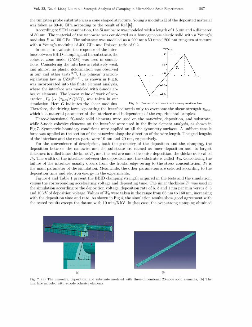
Three-dimensional 20-node solid elements were used on the nanowire, deposition, and substrate,while 8-node cohesive elements on the interface were used in the finite element analysis, as shown inFig.7. Symmetric boundary conditions were applied on all the symmetry surfaces. A uniform tensileforce was applied at the section of the nanowire along the direction of the wire length. The grid lengthsof the interface and the rest parts were 10 nm and 20 nm, respectively.
For the convenience of description, both the geometry of the deposition and the clamping, thedeposition between the nanowire and the substrate are named as inner deposition and its largestthickness is called inner thickness T1, and the rest are named as outer deposition, the thickness is calledT2. The width of the interface between the deposition and the substrate is called W0. Considering thefailure of the interface usually occurs from the frontal edge owing to the stress concentration, T1 isthe main parameter of the simulation. Meanwhile, the other parameters are selected according to thedeposition time and electron energy in the experiments.
Figure 4 and Table 1 present the EBID clamping strength acquired in the tests and the simulation,versus the corresponding accelerating voltage and depositing time. The inner thickness T1 was used inthe simulation according to the deposition voltage, deposition rate of 5, 3 and 1 nm per min versus 3, 5and 10 kV of deposition voltage. Values of W0 were taken in the range from 65 nm to 160 nm, increasingwith the deposition time and rate. As shown in Fig.4, the simulation results show good agreement withthe tested results except the datum with 10 min/5 kV. In that case, the over-strong clamping obtained
Fig. 7. (a) The nanowire, deposition, and substrate modeled with three-dimensional 20-node solid elements, (b) Theinterface modeled with 8-node cohesive elements.
· 588 · ACTA MECHANICA SOLIDA SINICA 2009
in the test could be attributed to some adhesion interaction with contaminators on the probe surface orto misalignment of the tensile load. A significant result is that we have retrieved τmax by combining theexperimental tests and numerical analysis, with its value in the range of 0.2-0.4 GPa for the interfaceof EBID-tungsten substrate at various experimental parameters. It is obvious that the cohesive zonemodeling gives us a way to estimate the shear resistance of the interface between the clamping and thesubstrate, by which the strength of EBID clamping in a specific SEM chamber could be predicted.
III. STRENGTH OF VAN DER WAALS FORCE BASED CLAMPINGWhen micro/nanowires are put on substrates or approached by microprobes, clamping between the
wire and the substrate or the probe will spontaneously form. This kind of clamping is mainly due tothe van de Waals interaction. In this section, the clamping strength of two most common configurationsbased on van der Waals interaction is discussed, including the micro/nanowire, the substrate and themicroprobe.
3.1. Clamping Strength between Microwire and Substrate
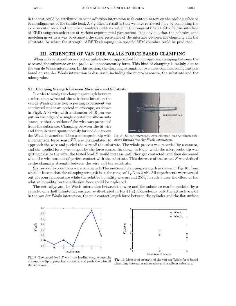
In order to study the clamping strength betweena micro/nanowire and the substrate based on thevan de Waals interaction, a peeling experiment wasconducted under an optical microscope, as shownin Fig.8. A Si wire with a diameter of 10 μm wasput on the edge of a single crystalline silicon sub-strate, so that a section of the wire was protrudedfrom the substrate. Clamping between the Si wireand the substrate spontaneously formed due to vander Waals interaction. Then a microprobe tip witha homemade force sensor[12] was manipulated to
Fig. 8 Silicon microcantilever clamped on the silicon sub-strate through van der Waals interaction.
approach the wire and peeled the wire off the substrate. The whole process was recorded by a camera,and the applied force was output by the force sensor. As shown in Fig.9, while the microprobe tip wasgetting close to the wire, the tested load F would increase until they get contacted, and then decreasedwhen the wire was out of perfect contact with the substrate. This decrease of the tested F was definedas the clamping strength between the wire and the substrate.
Six tests of two samples were conducted. The measured clamping strength is shown in Fig.10, fromwhich it is seen that the clamping strength is in the range of 1 μN to 2 μN. All experiments were carriedout at room temperature while the relative humidity was around 25%, in such a case the effect of therelative humidity on the adhesion force could be neglected.
Theoretically, van der Waals interaction between the wire and the substrate can be modeled by acylinder on a half infinite flat surface, as illustrated in Fig.11(a). Considering only the attractive partin the van der Waals interaction, the unit contact length force between the cylinder and the flat surface
Fig. 9. The tested load F with the loading step, where themicroprobe tip approaches, contacts, and peels the wire offthe substrate.
Fig. 10. Measured strength of the van der Waals force basedclamping between a micro wire and a silicon substrate.

Vol. 22, No. 6 Liang Liu et al.: Strength Analysis of Clamping in Micro/Nano Scale Experiments · 589 ·
Fig. 11. (a) Van der Waals force model between a cylinder of radius R and a flat surface, (b) Van der Waals force modelbetween two perpendicular cylinders of radius R1 and R2.
is[13]
Fvc =AH
√R
8√
2a5/2(1)
where a is the distance between the cylinder and the surface, AH = π2ρ1ρ2C the Hamaker constant,and ρ1, ρ2 the number of atoms per unit volume in the two bodies, respectively. For a silicon wire andsilicon substrate, the Hamaker constant is AH = 6.5 × 10⁻²⁰ J[14].
Note that in the cylinder-plane model, the van der Waals force between the wire and the substratedepends on the effective contact length Lc. Let Fvm = FvcLc, and the effective length Lc in our testcan be estimated by
Lc =8√
2a5/2Fvm
AH
√R
(2)
The values of Lc for the two samples in the tests are listed in Table 2, which are about 77 nm.As shown in Fig.8, the wire used in the test is not perfectly smooth and straight, and delamination of
the wire actually exists in some specific points, so that the contact between the wire and the substrateis more like a point contact. According to the van der Waals force model of a sphere-plane, the forceis[13]
Fvs =AHR
6a2(3)
where R is radius of the sphere. For R = 5 μm and a = 0.2 nm[15], the van der Waals force is Fvs = 1354nN. Table 2 gives comparison between the measured strength and the calculated strength through thesphere-plane model, from which it is seen that the calculated strength agrees well with the measuredstrength.
Table 2. Comparison between the measured and calculated van der Waals clamping strength
Sample No. d Calculated strength Fvs Averaged measured strength Fvm Lc
1 10 μm 1354 nN 1739 nN 76.6 nm2 10 μm 1354 nN 1751 nN 77.1 nm
3.2. Clamping Strength between Nanowire and Probe
When a nanowire is approached by a micromanipulator probe, van der Waals interaction betweenthem can be modeled by two perpendicular cylinders as illustrated in Fig.11(b). Thus, the force betweenthem is[13]
Fv12 =AH
√R1R2
6a2(4)
where R1 and R2 are the radius of the two cylinders, a the distance between the two cylinders and AH
the Hamaker constant. In case that the two bodies in interaction are made of different materials, theHamaker constant is approximated by[4,14]
AH =√
AH1AH2 (5)

· 590 · ACTA MECHANICA SOLIDA SINICA 2009
where AH1 and AH2 are Hamaker constants of the two materials respectively.An experiment was conducted in SEM to study
the van der Waals clamping between a siliconnanowire and a tungstenprobe.As shown inFig.12,the silicon nanowire was clamped with EBID onthe tungsten probe A, and the other probe B wasmanipulated to approach the nanowire. Clamp-ing forms immediately when the nanowire contactsprobe B.Then probeB wasmoved away fromprobeA to detach the nanowire. We observed that thenanowire did not dispart from probe B until a crit-ical displacement. With the largest deformation ofthe nanowire, the van der Waals clamping force
Fig. 12 SEM image of van der Waals force based clampingbetween a tungsten probe and a Si nanowire.
can be calculated. As shown in Fig.12, probe B contacts the nanowire on point C, D is the end of thecantilever, and lp is the distance between them, and Δp the deformation of the nanowire at point C.The test was repeated for 18 times, and the measured clamping strength between probe B and thesilicon nanowire is shown in Table 3. The average value of the 18 tested results is 7 nN.
Table 3. Test results of van der Waals clamping force between a W probe and a Si nanowire
No. lp (nm) Δp (nm) Fv12 (nN) No. lp (nm) Δp (nm) Fv12 (nN)
1 16725 1072 1.27 10 7892 748 6.902 12871 1632 4.02 11 6768 342 4.713 13038 762 1.81 12 6235 606 10.314 12683 388 0.99 13 5674 466 10.065 10012 1756 8.59 14 5640 435 9.546 9524 1664 9.31 15 5556 155 3.537 9036 1553 10.00 16 4126 297 13.948 9238 1150 6.98 17 3624 174 11.059 9036 388 2.50 18 2697 78 9.52
Theoretically, since the nanowire is made of silicon and the probe is made of tungsten, Hamakerconstants are 6.5×10⁻²⁰ J and 30×10−20 J for Si and tungsten respectively, leading to AH = 1.40×10⁻¹⁹
J. With R1 = 78 nm, R2 = 70 nm, a = 0.2 nm. van der Waal force between the nanowire and theprobe can be calculated through the perpendicular cylinder-cylinder model (Eq.(4)) and is 51.5 nN.Considering that roughness of the probe and the nanowire could decrease their van der Waal force bymore than 10% to 50%[14,16], the calculated results is reasonable.
IV. DISCUSSIONAmong the micro/nano clamping methods, EBID clamping is one of the most reliable methods that
can bear considerable tensile load on the clamped sample. Summarizing the previous test results[2,3,7–9]
and the results in this paper, the clamping strength (load) range can be from 100 nN to 20 μN, andbe controlled by adjusting the depositing acceleration voltage and time. As for the clamping based onthe van der Waals interaction, our peeling tests provide 7 nN clamping strength in the nanoscale and1.7 μN in the microscale, where the influences of relative humidity and electrostatic interaction are notconsidered.
In fact, the influence of relative humidity (RH) cannot be neglected if the value of RH is greater than30%[17] and the water film will form on the surfaces of both the sample and the substrate to producethe capillary interaction and change the clamping strength greatly. It was tested that the adhesionforce between an AFM tip and a sample surface could be raised by 100%[17], or even by 300% betweena micro Si3O4 sphere and a Si substrate[18], when the RH value is increased from 0% to 90%. In ourexperiments, the clamping force between a cylindrical tungsten wire and a signal crystalline siliconsubstrate was also tested, which increases from 32 μN to 265 μN when the RH was increased from 40%

Vol. 22, No. 6 Liang Liu et al.: Strength Analysis of Clamping in Micro/Nano Scale Experiments · 591 ·
to 90%. A broad adhesion force range with RH changing can provide flexible selection of the clampingstrength requirement where the micro/nano tests are not affected by the humidity environment.
To the electrostatic interaction, it is also an important factor in the clamping. In our SEM clampingexperiments, the nanowire would abruptly jump onto the probe when their distance reached a criticalvalue (∼100 nm). This phenomenon is supposed to be due to the electrostatic interaction between theprobe and the Si nanowire. This attractive interaction provides the pre-driven force to the consequentvan der Waals clamping.
Combining the relevant results and the work in this paper, the clamping strengths and performanceof some clamping methods are listed in Table 4. The size and the material of clamped samples, theapplication environments, and the corresponding clamping forces are given.
Table 4. Comparison on strength and performance of usually used micro/nano clamping
Principle Material Size Environment Load
EBIDCNT[1,6], B[2],
D: 10 nm-150 nm SEM/TEM0.1 μN-20 μN
C[7,8], Si NW∗ (Tensile)
van derSi wire∗ D: 157 nm/10 μm SEM/Low RH 7 nN/1.7 μN
Cu sphere[3] R: ∼10μm SEM 0.116 μNWaals
ZnO NW[4] Width: ∼200 nm AFM —
RHAFM Tip Si3N4
[17] R: ∼100 nm RH: 0-100% 30 nN-70 nN
Si3N4 sphere[18] D: ∼500 μm RH: 0-100% 100 μN-400 μNConsidered
W wire[19] D: ∼180 μm RH: 45-95% 30 μN-600 μN
D:Volt.:
Electrostatic Glass sphere[20] 300 V-1200 V ∼ 50μN100 μm∼800 μm
RH < 65%
Si NW[19] D: ∼157 nm SEM 0.025 nN-11.1 nN
∗ The results in this paper
V. CONCLUSIONAn approach combining tensile tests on Si nanowires and FEM simulation to calculate the strength
of EBID clamping is given in this paper. The strength parameter τmax of the interface between EBIDclamping and the substrate based on CZM is obtained as 0.2-0.4 GPa. The strength of EBID clampingin a specific SEM chamber could be calculated and predicted with this method.
The clamping based on the van der Waals interaction is also investigated both theoretically andexperimentally. Two types of clamping experiments are conducted and modeled. The clamping strengthsbetween a micro silicon wire and a silicon substrate, as well as a silicon nanowire and a tungsten probeare both tested and calculated.
The influences of relative humidity and the electrostatic interaction on micro/nano clamping arediscussed. The clamping strengths and performance of different clamping methods are also comparedconsidering the factors of the size and the material of clamped samples, and the application environments.
References[1] Chong,K.P., Nano science and engineering in solid mechanics. Acta Mechnica Solida Sinica, 2008, 20(2):
97-103.
[2] Yu,M.F., Oleg,L., Mark,J.D., Katerina,M., Thomas,F.K. and Rodney,S.R., Strength and breaking mech-anism of multiwalled carbon nanotubes under tensile load. Science, 2000, 287(5453): 637-640.
[3] Ding,W.Q., Lorenzo,C., Chen,X.Q., Kevin,M.K. and Rodney,S.R., Mechanics of crystalline boronnanowires. Composites Science and Technology, 2006, 66(9): 1112-1124.
[4] Feddema,J.T., Xavier,P. and Brown,R., Micro-assembly planning with van der Waals force. Journal of
Micromechatronics, 2001, 1(2): 139-153.

· 592 · ACTA MECHANICA SOLIDA SINICA 2009
[5] Mai,W.J. and Wang,Z.L., Quantifying the elastic deformation behavior of bridged nanobelts. Applied
Physics Letters, 2006, 89(7): 073112.[6] Ding,W.Q., Dikin,D.A., Chen,X.Q., Piner,R.D., Rodney,S.R. and Zussman,E., Mechanics of hydrogenated
amorphous carbon deposits from electron-beam-induced deposition of a paraf?n precursor. Journal of Ap-
plied Physics, 2005, 98(1): 014905.[7] Ding,W.Q., Lorenzo,C., Kohlhaas,K.M., Chen,X.Q., Dikin,D.A. and Rodney,S.R., Modulus, fracture
strength, and brittle vs. plastic response of the outer shell of arc-grown multi-walled carbon nanotubes.Experimental Mechanics, 2007, 47(1): 25-36.
[8] Kristian,M., Dorte,N.M., Soren,D. and Peter,B., Constructing, connecting and soldering nanostructuresby environmental electron beam deposition. Nanotechnology, 2004, 15(8): 1047-1053
[9] Zussman,E., Chen,X.Q., Ding,W.Q., Lorenzo,C., Dikin,D.A., Quintana,J.P. and Rodney,S.R., Mechanicaland structural characterization of electrospun PAN-derived carbon nanofibers. Carbon, 2005, 43(10): 2175-2185.
[10] Chandra,N., Li,H., Shet,C. and Ghonem,H., Some issues in the application of cohesive zone models formetal-ceramic interfaces. International Journal of Solids and Structures, 2002, 39(10): 2827-2855.
[11] Geubelle,P.H. and Baylor,J., Impact-induced delamination of laminated composites: A 2D simulation. Com-
posites Part B Engineering, 1998, 29(5): 589-602.[12] Li,X.D., Su,D.C. and Zhang,Z., A novel technique of microforce sensing and loading. Sensors and Actuators
A: Physical, 2009, 153(1): 13-23.[13] Jacob,N.I., Intermolecular and Surface Forces. London: Academic Press, 1992.[14] Yakov,I.R., Joshua,J.A., Ali,A., Rajiv,K.S. and Brij,M.M., Adhesion between nanoscale rough surfaces —
II. Measurement and comparison with theory. Journal of Colloid and Interface Science, 2000, 232(1): 17-24.[15] Marina,R. and Jacob,N.I., Nanotribology and Nanomechanics. Berlin: Springer, 2005.[16] Yakov,I.R., Joshua,J.A., Ali,A., Rajiv,K.S. and Brij,M.M., Adhesion between nanoscale rough surfaces —
I. Role of asperity geometry. Journal of Colloid and Interface Science, 2000, 232(1): 10-16.[17] Xiao,X.D. and Qian,L.M., Investigation of humidity-dependent capillary force. Langmuir, 2000, 16(21):
8153-8158.[18] Qing,T., Shao,T.M. and Wen,S.Z., Effects of relative humidity on surface adhesion. Tribology, 2006, 26(4):
295-299.