stress-controlled pb(zr0.52ti0.48)o3 thick films by ... · stress-controlled pb(zr0.52ti0.48)o3...
TRANSCRIPT

Stress-controlled Pb(Zr0.52Ti0.48)O3 thick films by thermal expansion mismatchbetween substrate and Pb(Zr0.52Ti0.48)O3 filmGuifang Han, Jungho Ryu, Woon-Ha Yoon, Jong-Jin Choi, Byung-Dong Hahn, Jong-Woo Kim, Dong-Soo Park,Cheol-Woo Ahn, Shashank Priya, and Dae-Yong Jeong Citation: Journal of Applied Physics 110, 124101 (2011); doi: 10.1063/1.3669384 View online: http://dx.doi.org/10.1063/1.3669384 View Table of Contents: http://scitation.aip.org/content/aip/journal/jap/110/12?ver=pdfcov Published by the AIP Publishing Articles you may be interested in Nanosheet controlled epitaxial growth of PbZr0.52Ti0.48O3 thin films on glass substrates Appl. Phys. Lett. 105, 132904 (2014); 10.1063/1.4896991 Piezoelectrically induced mechano-catalytic effect for degradation of dye wastewater through vibratingPb(Zr0.52Ti0.48)O3 fibers Appl. Phys. Lett. 104, 162907 (2014); 10.1063/1.4873522 Misfit strain dependence of ferroelectric and piezoelectric properties of clamped (001) epitaxialPb(Zr0.52,Ti0.48)O3 thin films Appl. Phys. Lett. 99, 252904 (2011); 10.1063/1.3669527 Microstress relaxation effect of Pb ( Zr 0.52 Ti 0.48 ) O 3 films with thicknesses for micro/nanopiezoelectricdevice Appl. Phys. Lett. 96, 092904 (2010); 10.1063/1.3330897 Magnetoelectric effects of nanoparticulate Pb ( Zr 0.52 Ti 0.48 ) O 3 – Ni Fe 2 O 4 composite films Appl. Phys. Lett. 89, 102907 (2006); 10.1063/1.2338766
[This article is copyrighted as indicated in the article. Reuse of AIP content is subject to the terms at: http://scitation.aip.org/termsconditions. Downloaded to ] IP:
128.173.126.47 On: Thu, 07 May 2015 17:54:09
Stress-controlled Pb(Zr0.52Ti0.48)O3 thick films by thermal expansionmismatch between substrate and Pb(Zr0.52Ti0.48)O3 film
Guifang Han,1 Jungho Ryu,1,a) Woon-Ha Yoon,1 Jong-Jin Choi,1 Byung-Dong Hahn,1
Jong-Woo Kim,1 Dong-Soo Park,1 Cheol-Woo Ahn,1 Shashank Priya,2
and Dae-Yong Jeong3,a)
1Functional Ceramics Group, Korea Institute of Materials Science (KIMS), Changwon, Gyeongnam 641-831,Korea2Department of Materials Science and Engineering, Virginia Tech., Blacksburg, Virginia 24061, USA3School of Materials Engineering, Inha University, Incheon 402-751, Korea
(Received 14 June 2011; accepted 11 November 2011; published online 16 December 2011)
Polycrystalline Pb(Zr0.52Ti0.48)O3 (PZT) thick films (thickness �10 lm) were successfully
fabricated by using a novel aerosol deposition technique on Si wafer, sapphire, and single crystal
yitria stabilized zirconia (YSZ) wafer substrates with Pt electrodes and their dielectric, ferroelectric,
and piezoelectric properties, and in-plane stresses were investigated. The films with different stress
conditions were simply controlled by the coefficient of thermal expansion (CTE) misfit of PZT films
and substrates. The results showed that the films bearing in-plane compressive stress deposited on
the YSZ and sapphire substrates have superior dielectric, ferroelectric (�90%), and piezoelectric
(>200%) properties over that of the Si wafer. Among these three substrates, YSZ shows superior
properties of the PZT films. However, films on Si wafer with tensile stress present lower properties. We
believed that in-plane compressive stresses within the films are benefited, the formation of c-domain
parallel to the thickness direction resulting in the higher piezoelectric properties. These results suggest
that the properties of polycrystalline PZT thick films can be adjusted by simply choosing the substrates
with different CTEs. VC 2011 American Institute of Physics. [doi:10.1063/1.3669384]
I. INTRODUCTION
Recently, it has been reported that the stress or strain
can significantly affect the physical and electric properties of
ferroelectric materials.1–3 In epitaxial BaTiO3 thin films,
biaxial compressive strain resulted in a higher ferroelectric
transition temperature (approximately 500 �C) and enhance-
ment of remnant polarization (at least 250%) compared to
bulk BaTiO3 ceramics.1 The stress magnitude and sign can
be controlled by the interface between the film and substrate
which have small lattice misfit strain. Regarding the electri-
cal properties with residual stress level, Lee et al. reported
that the ferroelectric properties of (111) oriented Pb(Zr,Ti)O3
(PZT) thin films were enhanced by inducing compressive
stress, which was introduced during annealing by bending
the substrate.2,3 Tuttle et al.4 have also shown that the highly
oriented PZT thin films (thickness is 300 nm) under compres-
sive residual stress exhibited superior ferroelectric properties
compared to the bulk polycrystalline ferroelectrics. How-
ever, prior studies are mostly based on the epitaxial thin
films or require a special fixture to control the stress. The
epitaxial film’s thickness is difficult to fabricate with over
1 lm-thick because of the critical stress relaxing thickness.
In practical piezoelectric applications of high power actua-
tors, high sensitivity sensors, and energy harvesting devices,
epitaxial grown or carefully orientation controlled piezoelec-
tric films have limited use, because of high production cost
and productivity. Thus, there is a critical need to understand
the physical behavior of thick polycrystalline films and iden-
tify the process to modulate the piezoelectric response. In
this study, we report �90% and 200% enhancements of fer-
roelectric and piezoelectric properties in PZT thick films,
respectively, by controlling the magnitude of interfacial
stress simply by choosing substrates with different coeffi-
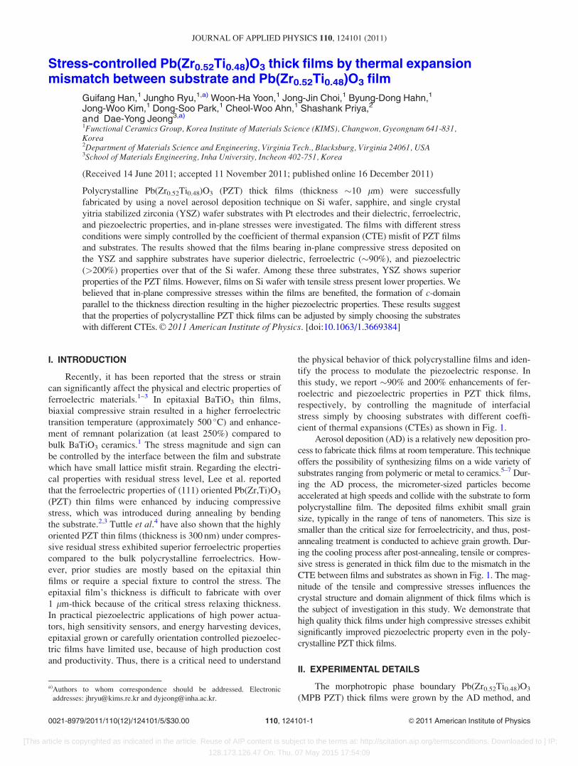
cient of thermal expansions (CTEs) as shown in Fig. 1.
Aerosol deposition (AD) is a relatively new deposition pro-
cess to fabricate thick films at room temperature. This technique
offers the possibility of synthesizing films on a wide variety of
substrates ranging from polymeric or metal to ceramics.5–7 Dur-
ing the AD process, the micrometer-sized particles become
accelerated at high speeds and collide with the substrate to form
polycrystalline film. The deposited films exhibit small grain
size, typically in the range of tens of nanometers. This size is
smaller than the critical size for ferroelectricity, and thus, post-
annealing treatment is conducted to achieve grain growth. Dur-
ing the cooling process after post-annealing, tensile or compres-
sive stress is generated in thick film due to the mismatch in the
CTE between films and substrates as shown in Fig. 1. The mag-
nitude of the tensile and compressive stresses influences the
crystal structure and domain alignment of thick films which is
the subject of investigation in this study. We demonstrate that
high quality thick films under high compressive stresses exhibit
significantly improved piezoelectric property even in the poly-
crystalline PZT thick films.
II. EXPERIMENTAL DETAILS
The morphotropic phase boundary Pb(Zr0.52Ti0.48)O3
(MPB PZT) thick films were grown by the AD method, and
a)Authors to whom correspondence should be addressed. Electronic
addresses: [email protected] and [email protected].
0021-8979/2011/110(12)/124101/5/$30.00 VC 2011 American Institute of Physics110, 124101-1
JOURNAL OF APPLIED PHYSICS 110, 124101 (2011)
[This article is copyrighted as indicated in the article. Reuse of AIP content is subject to the terms at: http://scitation.aip.org/termsconditions. Downloaded to ] IP:
128.173.126.47 On: Thu, 07 May 2015 17:54:09
single crystal silicon wafer (Si (100), Inostek Inc., Korea),
c-cut sapphire (0001), and yitria stabilized zirconia (YSZ)
with Ti=Pt bottom electrode were used as substrates. Regent
grade raw materials of PbO, ZrO2, and TiO2 (Aldrich Co.,
Milwaukee, WI) were mixed in their appropriate proportion
and ball milled for 24 h. After drying, the powder mixture
was calcined at 800 �C=5 h to obtain the PZT powder for the
AD process. All the �10 lm thick films were annealed at
700 �C for 1 h. The phases of the deposited films were identi-
fied by X-ray diffractometry. The residual stresses of the
films were analyzed by a high-resolution X-ray diffraction
system (HR-XRD, X’pert Pro MRD, Philips, Netherlands).
The microstructures of the film surface and fracture section
were identified by scanning electron microscopy (SEM:
JSM-5800, JEOL CO., Tokyo, Japan). A U1 mm Pt top
electrode was deposited to measure the electric properties
by direct current sputtering method. The poling condition
was 150 kV cm–1, 40 min, and 100 �C. The dielectric
measurement was carried out by using an impedance ana-
lyzer (4294A, Agilent, USA). The polarization-electric field
(P-E) hysteresis loops were recorded by a standardized ferro-
electric test system (P-LC100-K, Radiant Technologies). The
piezoelectric coefficients (d33eff) of the poled films were meas-
ured by both a d33-meter and laser beam interferometer.8
III. RESULTS AND DISCUSSION
In order to control the stress in PZT films, three single
crystals with varying CTEs were employed as the substrates
as shown in Fig. 1. Initially, the formation of thick PZT films
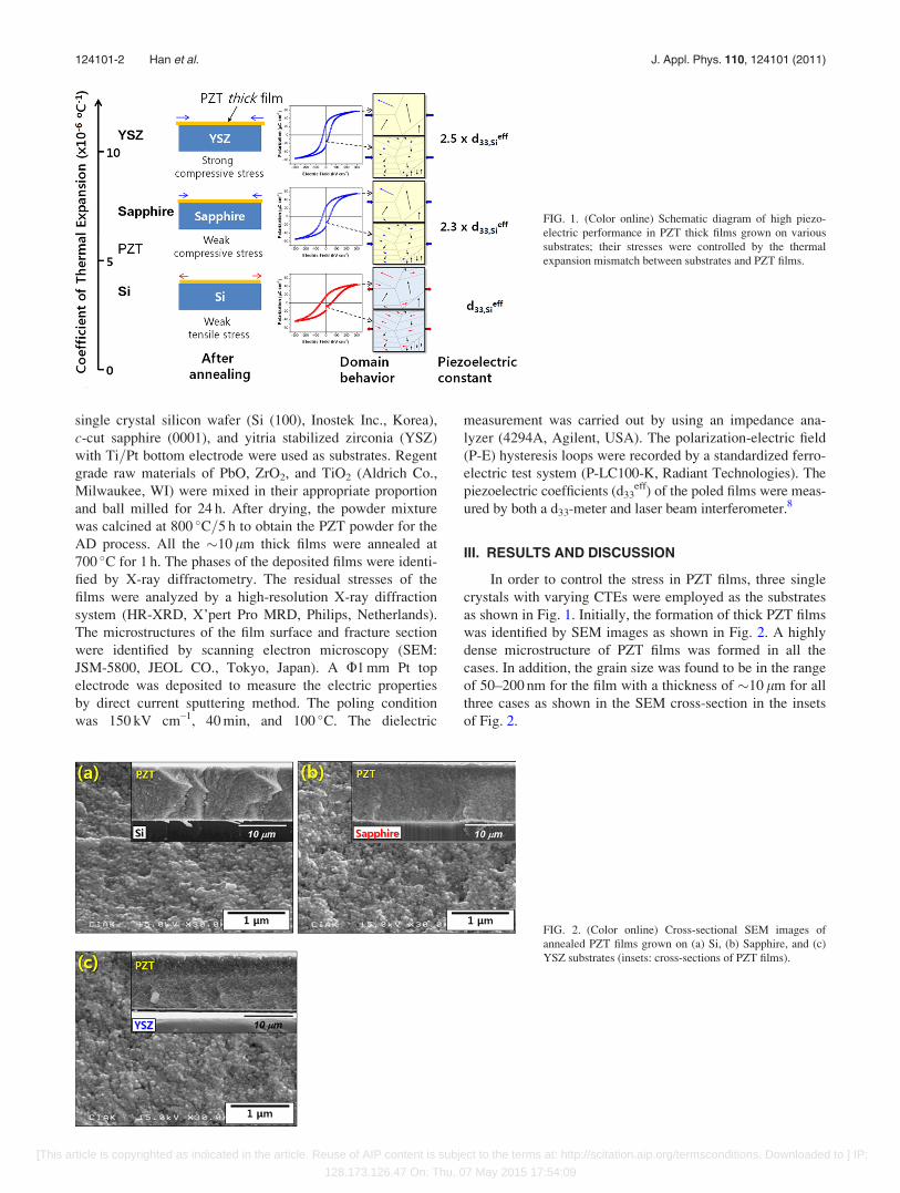
was identified by SEM images as shown in Fig. 2. A highly
dense microstructure of PZT films was formed in all the
cases. In addition, the grain size was found to be in the range
of 50–200 nm for the film with a thickness of �10 lm for all
three cases as shown in the SEM cross-section in the insets
of Fig. 2.
FIG. 1. (Color online) Schematic diagram of high piezo-
electric performance in PZT thick films grown on various
substrates; their stresses were controlled by the thermal
expansion mismatch between substrates and PZT films.
FIG. 2. (Color online) Cross-sectional SEM images of
annealed PZT films grown on (a) Si, (b) Sapphire, and (c)
YSZ substrates (insets: cross-sections of PZT films).
124101-2 Han et al. J. Appl. Phys. 110, 124101 (2011)
[This article is copyrighted as indicated in the article. Reuse of AIP content is subject to the terms at: http://scitation.aip.org/termsconditions. Downloaded to ] IP:
128.173.126.47 On: Thu, 07 May 2015 17:54:09
Compared with CTE of PZT (af¼ 5.5 ppm K�1), silicon
(asi¼ 3.5 ppm K�1) has the smaller value, while both sap-
phire (asap¼ 7.5 ppm K�1) and YSZ (aYSZ¼ 11 ppm K�1)
have the larger values as shown in Fig. 1.9–14 Hence, as
exhibited in Figs. 3 and 1, during the cooling process, tensile
stress was generated in PZT films grown on Si substrate
while films on sapphire and YSZ substrates showed the op-
posite phenomenon.
X-ray diffraction patterns of the annealed PZT films are
shown in Fig. 4. Except for the peaks of the Pt bottom elec-
trode and substrate, all the annealed PZT films showed a typ-
ical perovskite structure. The peaks of PZT films on sapphire
and YSZ substrates were shifted to a higher angle in compar-
ison to PZT film grown on Si substrate as shown in the inset
of Fig. 4. Thus, it could be suggested that the PZT films on
sapphire and YSZ substrates had a smaller lattice constant
compared to the films on Si substrates. The variation of lat-
tice parameters is an indication of the residual stress gener-
ated by the CTE mismatch between the PZT films and
substrates as listed in Fig. 1, Figs. 3 and 4, and Table I.
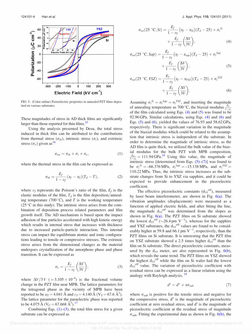
In order to investigate the domain reorientation with an
electric field, the P-E hysteresis loop was measured under a
high electric field at low frequency as presented in Fig. 5.
All the PZT films showed typical ferroelectric characteris-
tics, but the films on Si substrate exhibited the lowest
remnant and saturated polarizations and highest coercive
field. On the contrary, the films on YSZ substrate showed the
highest remnant and saturated polarizations with the lowest
coercive field. Because of the CTE mismatch between films
and substrates, the films on sapphire and YSZ substrates
have compressive stresses, with those on YSZ having the
highest compressive stress. Thus, it could be expected that
the domain alignment along the applied field direction is
facilitated. Since the grain size in our thick films is above the
critical grain size, the 90� domains will be readily formed as
the film is cooled through the Curie temperature to minimize
the effect of the stress. Especially, it could, therefore, be
expected that the domain alignment at 3 directions might be
easier for the PZT films on sapphire and YSZ substrates than
Si substrate; this is due to the compressive stress in PZT
films as indicated in Fig. 1. Furthermore, the compressive
stress along the plane direction could squeeze the Ti4þ=Zr4þ
ions along the thickness direction and give the large polariza-
tion and piezoelectric constant. However, the tensile stress,
in the PZT film on Si substrate, gave the opposite effect
resulting in the decrease of the amount of c-domain, polar-
ization, and piezoelectric constant. The summaries of electri-
cal properties of the PZT thick films are presented in Table I.
To precisely calculate the total stresses in PZT films, in-
plane residual stress was determined from the sin2w X-ray dif-
fraction technique at (211) peak (2h angle of�55.4�) as shown
in Fig. 3. Table I lists the magnitudes of residual stresses
for PZT films grown on Si, sapphire, and YSZ substrates. The
calculated magnitude of stress was found to be rtot(25 �C,
Si)¼þ119.5 6 4.1 (tensile), rtot(25 �C, Sap)¼ –131.5 6 1.1
(compressive), and rtot(25 �C, YSZ)¼ –270.6 6 4.9 MPa.
FIG. 3. (Color online) Variation of stress analysis based on d-spacing with
different Psi orientations of the sample by HR-XRD (X’pert Pro MRD, Phi-
lips, Netherlands), 2 h� 55� (112).
FIG. 4. (Color online) XRD patterns (top figures: variations of lattice pa-
rameters by tensile and compressive stresses) of PZT films deposited on var-
ious substrates.
TABLE I. In-plane stress and electric=piezoelectric properties in PZT films deposited on various substrates.
Substrate In-plane stress(MPa) d33eff(pC N–1) d33
eff(pm V–1) er(1 kHz) tan d(1 kHz) DPr=2(lC cm–2) DEc=2(kV cm–1)
Silicon 119.5 6 4.1(Tensile) 50 26.4 1026 0.025 17.0 52.6
Sapphire –131.5 6 1.1(Compressive) 80 59.8 1260 0.023 23.4 37.4
YSZ –270.6 6 4.9(Compressive) 95 66.1 1265 0.039 25.5 30.0
124101-3 Han et al. J. Appl. Phys. 110, 124101 (2011)
[This article is copyrighted as indicated in the article. Reuse of AIP content is subject to the terms at: http://scitation.aip.org/termsconditions. Downloaded to ] IP:
128.173.126.47 On: Thu, 07 May 2015 17:54:09
These magnitudes of stress in AD thick films are significantly
larger than those reported for thin films.15
Using the analysis presented by Desu, the total stress
induced in thick film can be attributed to the contributions
from thermal stress (rth), intrinsic stress (ri), and extrinsic
stress (re) given as16
rtot ¼ rth þ ri þ re; (1)
where the thermal stress in the film can be expressed as
rth ¼Ef
1� �fðaf � aSÞðTd � TÞ; (2)
where �f represents the Poisson’s ratio of the film, Ef is the
elastic modulus of the film, Td is the film deposition=anneal-
ing temperature (700 �C), and T is the working temperature
(25 �C in this study). The intrinsic stress arises from the com-
bination of deposition process related parameters and film
growth itself. The AD mechanism is based upon the impact
adhesion of fine particles accelerated with high kinetic energy
which results in internal stress that increases with thickness
due to increased particle-particle interaction. This internal
stress can impact the equilibrium atomic and ionic configura-
tions leading to tensile or compressive stresses. The extrinsic
stress arises from the dimensional changes as the material
undergoes crystallization of the amorphous phase and phase
transition. It can be expressed as
re ¼Ef
1� �f
DV
3V
� �; (3)
where DV=3 V (¼ 3.105� 10–4) is the fractional volume
change in the PZT film near MPB. The lattice parameters for
the tetragonal phase in the vicinity of MPB have been
reported to be aT¼ 4.041 A and cT¼ 4.140 A (VT¼ 67.6 A3).
The lattice parameter for the paraelectric phase was reported
to be 4.075 A (VC¼ 67.668 A3).17
Combining Eqs. (1)–(3), the total film stress for a given
substrate can be expressed as
rtotð25 �C; SiÞ ¼ Ef
1� �faf � aSi
� �ðTd � 25Þ þ ri
Si
þ Ef
1� �f
DV
3V
� �; (4)
rtotð25 �C; SapÞ ¼ Ef
1� �faf � asap
� �ðTd � 25Þ þ ri
Sap
þ Ef
1� �f
DV
3V
� �; (5)
rtotð25 �C; YSZÞ ¼ Ef
1� �faf � aYSZ
� �ðTd � 25Þ þ ri
YSZ
þ Ef
1� �f
DV
3V
� �: (6)
Assuming riSi ¼ ri
Sap ¼ riYSZ, and inserting the magnitude
of annealing temperature as 700 �C, the biaxial modulusEf
1��f
of the film calculated using Eqs. (4) and (5) was found to be
92.96 GPa. Similar calculations, using Eqs. (4) and (6) and
Eqs. (5) and (6), yielded the values of 76.93 and 58.62 GPa,
respectively. There is significant variation in the magnitude
of the biaxial modulus which could be related to the assump-
tion that intrinsic stress is independent of the substrate. In
order to determine the magnitude of intrinsic stress, as the
AD film is quite thick, we utilized the bulk value of the biax-
ial modulus for the bulk PZT with MPB composition,Eb
1��b¼ 111:94 GPa.18 Using this value, the magnitude of
intrinsic stress [determined from Eqs. (5)–(7)] was found to
be riSi ¼ –66.376 MPa, ri
Sap ¼ –15.138 MPa, and riYSZ ¼
110.22 MPa. Thus, the intrinsic stress increases as the sub-
strate changes from Si to YSZ via sapphire, and it could be
expected to provide enhancement in the piezoelectric
coefficient.
The effective piezoelectric constants (d33eff), measured
by laser beam interferometer, are shown in Fig. 6(a). The
vibration amplitudes (displacement) were measured as a
function of applied electric fields, and after fitting the line,
the magnitude d33eff was determined from the slopes as
shown in Fig. 6(a). The PZT films on Si substrate showed
the lowest d33eff (�26.4 pm V�1), whereas for the sapphire
and YSZ substrates, the d33eff values are found to be consid-
erably higher at 59.8 and 66.1 pm V�1, respectively, than the
PZT films on Si substrate. It is interesting that the PZT film
on YSZ substrate showed a 2.5 times higher d33eff than the
film on Si substrate. The direct piezoelectric constants, meas-
ured by the d33 meter, are also represented in Fig. 6(b),
which reveals the same trend. The PZT films on YSZ showed
the highest d33eff while the film on Si wafer had the lowest
d33eff value. The variation of piezoelectric coefficient with
residual stress can be expressed as a linear relation using the
analogy with Rayleigh analysis, 19
ds ¼ do þ arsub ð7Þ
where rsub is positive for the tensile stress and negative for
the compressive stress, do is the magnitude of piezoelectric
coefficient at zero residual stress, and ds is the magnitude of
piezoelectric coefficient at the residual stress of magnitude
rsub. Fitting the experimental data as shown in Fig. 6(b), the
FIG. 5. (Color online) Ferroelectric properties in annealed PZT films depos-
ited on various substrates.
124101-4 Han et al. J. Appl. Phys. 110, 124101 (2011)
[This article is copyrighted as indicated in the article. Reuse of AIP content is subject to the terms at: http://scitation.aip.org/termsconditions. Downloaded to ] IP:
128.173.126.47 On: Thu, 07 May 2015 17:54:09
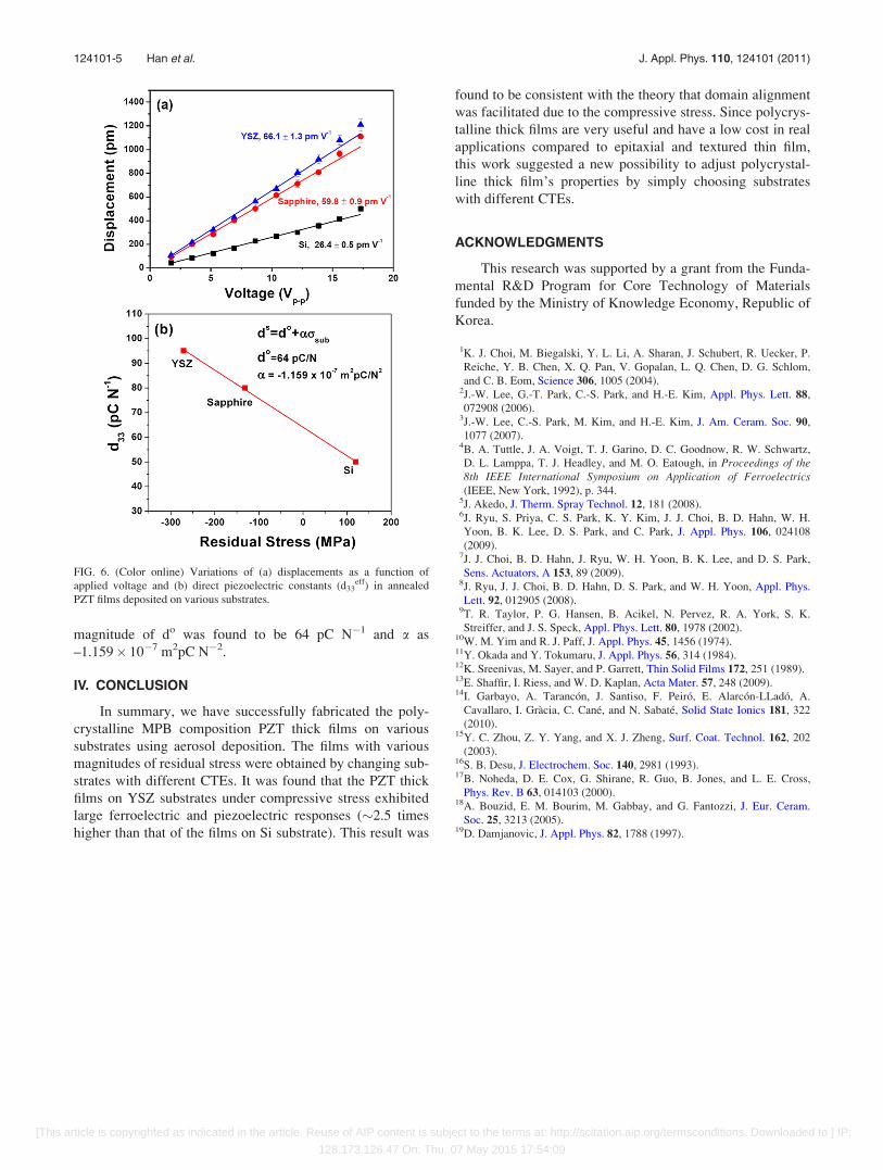
magnitude of do was found to be 64 pC N�1 and a as
–1.159� 10�7 m2pC N�2.
IV. CONCLUSION
In summary, we have successfully fabricated the poly-
crystalline MPB composition PZT thick films on various
substrates using aerosol deposition. The films with various
magnitudes of residual stress were obtained by changing sub-
strates with different CTEs. It was found that the PZT thick
films on YSZ substrates under compressive stress exhibited
large ferroelectric and piezoelectric responses (�2.5 times
higher than that of the films on Si substrate). This result was
found to be consistent with the theory that domain alignment
was facilitated due to the compressive stress. Since polycrys-
talline thick films are very useful and have a low cost in real
applications compared to epitaxial and textured thin film,
this work suggested a new possibility to adjust polycrystal-
line thick film’s properties by simply choosing substrates
with different CTEs.
ACKNOWLEDGMENTS
This research was supported by a grant from the Funda-
mental R&D Program for Core Technology of Materials
funded by the Ministry of Knowledge Economy, Republic of
Korea.
1K. J. Choi, M. Biegalski, Y. L. Li, A. Sharan, J. Schubert, R. Uecker, P.
Reiche, Y. B. Chen, X. Q. Pan, V. Gopalan, L. Q. Chen, D. G. Schlom,
and C. B. Eom, Science 306, 1005 (2004).2J.-W. Lee, G.-T. Park, C.-S. Park, and H.-E. Kim, Appl. Phys. Lett. 88,
072908 (2006).3J.-W. Lee, C.-S. Park, M. Kim, and H.-E. Kim, J. Am. Ceram. Soc. 90,
1077 (2007).4B. A. Tuttle, J. A. Voigt, T. J. Garino, D. C. Goodnow, R. W. Schwartz,
D. L. Lamppa, T. J. Headley, and M. O. Eatough, in Proceedings of the8th IEEE International Symposium on Application of Ferroelectrics(IEEE, New York, 1992), p. 344.
5J. Akedo, J. Therm. Spray Technol. 12, 181 (2008).6J. Ryu, S. Priya, C. S. Park, K. Y. Kim, J. J. Choi, B. D. Hahn, W. H.
Yoon, B. K. Lee, D. S. Park, and C. Park, J. Appl. Phys. 106, 024108
(2009).7J. J. Choi, B. D. Hahn, J. Ryu, W. H. Yoon, B. K. Lee, and D. S. Park,
Sens. Actuators, A 153, 89 (2009).8J. Ryu, J. J. Choi, B. D. Hahn, D. S. Park, and W. H. Yoon, Appl. Phys.
Lett. 92, 012905 (2008).9T. R. Taylor, P. G. Hansen, B. Acikel, N. Pervez, R. A. York, S. K.
Streiffer, and J. S. Speck, Appl. Phys. Lett. 80, 1978 (2002).10W. M. Yim and R. J. Paff, J. Appl. Phys. 45, 1456 (1974).11Y. Okada and Y. Tokumaru, J. Appl. Phys. 56, 314 (1984).12K. Sreenivas, M. Sayer, and P. Garrett, Thin Solid Films 172, 251 (1989).13E. Shaffir, I. Riess, and W. D. Kaplan, Acta Mater. 57, 248 (2009).14I. Garbayo, A. Tarancon, J. Santiso, F. Peiro, E. Alarcon-LLado, A.
Cavallaro, I. Gracia, C. Cane, and N. Sabate, Solid State Ionics 181, 322
(2010).15Y. C. Zhou, Z. Y. Yang, and X. J. Zheng, Surf. Coat. Technol. 162, 202
(2003).16S. B. Desu, J. Electrochem. Soc. 140, 2981 (1993).17B. Noheda, D. E. Cox, G. Shirane, R. Guo, B. Jones, and L. E. Cross,
Phys. Rev. B 63, 014103 (2000).18A. Bouzid, E. M. Bourim, M. Gabbay, and G. Fantozzi, J. Eur. Ceram.
Soc. 25, 3213 (2005).19D. Damjanovic, J. Appl. Phys. 82, 1788 (1997).
FIG. 6. (Color online) Variations of (a) displacements as a function of
applied voltage and (b) direct piezoelectric constants (d33eff) in annealed
PZT films deposited on various substrates.
124101-5 Han et al. J. Appl. Phys. 110, 124101 (2011)
[This article is copyrighted as indicated in the article. Reuse of AIP content is subject to the terms at: http://scitation.aip.org/termsconditions. Downloaded to ] IP:
128.173.126.47 On: Thu, 07 May 2015 17:54:09