strong light–matter interactions ... · strong light–matter interactions enabled by polaritons...
TRANSCRIPT

1901473 (1 of 25) © 2020 WILEY-VCH Verlag GmbH & Co. KGaA, Weinheim
www.advopticalmat.de
REVIEW
Strong Light–Matter Interactions Enabled by Polaritons in Atomically Thin Materials
P. A. D. Gonçalves, Nicolas Stenger, Joel D. Cox, N. Asger Mortensen,* and Sanshui Xiao*
DOI: 10.1002/adom.201901473
1. Introduction
Since the initial isolation in 2004(–2005) of single-layer graphene by mechanical exfo-liation,[1,2] a massive body of research on graphene and other atomically thin mate-rials has been growing rapidly, further catalyzed by novel physics arising in the 2D limit and also by the steady progress of nanofabrication technology. In par-ticular, advanced fabrication techniques now enable unprecedented control over material growth, quality, and customiza-tion, facilitating both the isolation of new 2D materials and their availability. Nowa-days, ultrafast epitaxial growth of large-scale single-crystal graphene is achievable by situ modulation of the vapor-phase reactants,[3–5] compositionally modulated MoS2–MoSe2 and WS2–WSe2 lateral het-erostructures have been reported,[6] and correlated insulator behavior has been observed in stacked graphene sheets twisted by a magic angle of 1.1°.[7,8] Recent developments in vdW integration of 2D materials present alternative ways to create vdW heterostructures with unique and desirable electronic and optical pro-perties that are unavailable in isolated 2D materials.[9,10] All of these advances have
triggered fundamental explorations of newly developed 2D and vdW heterostructures, stimulating investigation of their poten-tial applications in energy harvesting,[11–14] photonics and opto-electronics,[15–22] and biomedical technologies.[23–28]
Due to their atomic-scale thickness, light–matter interac-tions in 2D materials are often weak; for this reason, the strong light–matter interactions in 2D and vdW heterostructures that have been observed are often fueled by polaritonic excita-tions.[29–34] These polaritonic waves can have extremely small in-plane wavelengths λp compared to their associated free-space light wavelength λ0 (see Figure 1). For example, the light con-finement factor λ0/λp can reach ≈50 for hyperbolic phonon polaritons,[35–37] and even ≈220 for plasmon polaritons in high-quality graphene encapsulated by hexagonal boron nitride (hBN) and in graphene moiré superlattices.[38,39] The strong light concentration associated with 2D polaritons gives rise to an extremely large local density of electromagnetic states, resulting in strong light–matter interactions. Very recently, the anisotropic polariton propagation in the natural vdW material α-MoO3 has been reported[40] to exhibit ultralow loss, ten times
Polaritons, resulting from the hybridization of light with polarization charges formed at the boundaries between media with positive and negative dielec-tric response functions, can focus light into regions much smaller than its associated free-space wavelength. This property is paramount for a plethora of applications in nanophotonics, ranging from biological sensing to pho-tocatalysis to nonlinear and quantum optics. In the two-dimensional (2D) limit, represented by atomically thin and van der Waals (vdW) materials of single-layers bound by weak vdW attraction, polaritons are characterized by extremely small wavelengths associated with extreme optical confinement, and furthermore can exhibit long lifetimes, electrical tunability, and extreme sensitivity to their dielectric environment, among many other desirable quali-ties in nano-optical device applications. Here, the fundamentals of polari-tons in atomically thin materials are summarized, emphasizing plasmon and exciton polaritons, their strong light–matter interactions, and nonlinear plasmonics. More specifically, this review opens with a pedagogical discus-sion of plasmons in extended and nanostructured graphene, providing a classical electrodynamical model in a nonretarded theoretical framework, and the ultraconfined acoustic plasmons supported by hybrid graphene–dielectric–metal structures. In addition, the basic principles are introduced and the recent developments on nonlinear graphene plasmonics and on strong coupling physics with atomically thin transition metal dichalcogenides are reviewed. Finally, potentially new, promising research directions in the burgeoning field of 2D nanophotonics are identified.
Dr. P. A. D. Gonçalves, Prof. N. Stenger, Prof. S. XiaoDepartment of Photonics EngineeringTechnical University of DenmarkDK-2800 Kongens Lyngby, DenmarkE-mail: [email protected]. P. A. D. Gonçalves, Prof. N. Stenger, Prof. N. A. Mortensen, Prof. S. XiaoCenter for Nanostructured GrapheneTechnical University of DenmarkDK-2800 Kongens Lyngby, DenmarkE-mail: [email protected]. P. A. D. Gonçalves, Prof. J. D. Cox, Prof. N. A. MortensenCenter for Nano OpticsUniversity of Southern DenmarkDK-5230 Odense M, DenmarkProf. J. D. Cox, Prof. N. A. MortensenDanish Institute for Advanced StudyUniversity of Southern DenmarkDK-5230 Odense M, Denmark
The ORCID identification number(s) for the author(s) of this article can be found under https://doi.org/10.1002/adom.201901473.
Adv. Optical Mater. 2020, 1901473

www.advancedsciencenews.com
© 2020 WILEY-VCH Verlag GmbH & Co. KGaA, Weinheim1901473 (2 of 25)
www.advopticalmat.de
smaller than that of graphene plasmon polaritons at room tem-perature,[38] together with strong optical field confinement, with λ0/λp ≈ 60. The realization of actively tunable and long-lived polaritons in atomically thin materials presents a new frontier in nanophotonics to control light on length scales well below the diffraction limit. This review presents an overview of the fundamentals of polaritonic physics in extended and structured 2D materials, with an emphasis on plasmon and exciton polari-tons, and their strong light–matter interactions.
2. Graphene Plasmon Polaritons
The most prominent example of a 2D polariton in the literature is unarguably the graphene plasmon polariton.[30,41,42] Doped graphene supports plasmon polaritons across the terahertz (THz) and mid-infrared (mid-IR) spectral ranges and it is often regarded as an excellent plasmonic material.[30,38,41–44] Some of the enticing properties of graphene plasmons[30,41,42] are consequence of graphene’s tantalizing electronic and optical properties,[41,45] while others are simply related to its two-dimensionality.[41,46] Nonetheless, the unique electronic struc-ture of graphene is of paramount importance for many of its alluring polaritonic features.[32,41,42] In addition, the mechanical stability of graphene[47] together with its intrinsic atomic thick-ness makes it particularly appealing also from a technological standpoint.[48]
A key advantage of graphene plasmons—particularly when compared with traditional surface plasmons supported by 3D metals—is the ability to actively control the frequency of plasmon resonances in graphene simply by tuning its Fermi level,[49–52] which may be achieved by means of electrostatic gating[50,51] or by chemical doping.[53] Another noteworthy advantage of graphene plasmon polaritons is that they can propagate while experiencing relatively low losses when com-pared with traditional plasmonic materials (this is particularly true for graphene encapsulated in hBN).[30,38,43]
In the following, we present an overview of the elemen-tary physics governing plasmonic excitations in graphene. We begin by considering propagating plasmon polaritons sup-ported by an extended, continuous graphene sheet, and then move on to the theoretical description of localized plasmons in graphene nanostructures. Finally, it should be noted that although here particular emphasis is given to plasmons in gra-phene, the theoretical methodology introduced in this section can be straightforwardly applied to other polaritonic excita-tions[29,30] in the ever-increasing number[54] of 2D and quasi-2D materials.[55,56]
2.1. Plasmons in Extended Graphene
We consider a graphene monolayer sandwiched between two dielectric media, characterized by the relative permittivities ε1 and ε2. The dispersion relation of transverse magnetic (TM) plasmon polaritons propagating along the graphene sheet is straightforwardly derived by matching the fields on either side of the interface,[41] similarly to the derivation of the disper-sion of surface plasmon polaritons (SPPs) in dielectric–metal interfaces. The crucial difference here is that the presence of graphene is taken into account by introducing a nonvanishing surface current density, 2DJJ , which enters in the boundary con-ditions. For a uniform graphene layer—i.e., unstrained, unpat-terned, pristine graphene—the induced surface current due to an electric field is given by 2DJJ EE
σ= , where σ σ(q, ω) is the (in general nonlocal) conductivity of graphene,[41] and EE
is the total in-plane electric field evaluated at the position of the graphene sheet. With the above-noted considerations, the dis-persion relation of graphene plasmons (GPs) stems from the following implicit condition[41]
q k q k
i qεε
εε
σ ωωε−
+−
+ =( , )
01
202
1
2
202
2 0
(1)
Adv. Optical Mater. 2020, 1901473
Figure 1. Schematic of polaritons in atomically thin materials. In the 2D limit, polaritons are excited in the plane of an atomically thin crystal by light at frequencies where the imaginary part of the 2D optical conductivity σ2D and the dielectric permittivity of the background medium εb are both positive. The polariton wavelength λp is much smaller than the impinging light wavelength λ0, with the associated electric field confined within a distance ≈λp/2π of the film; this concentrated near-field drives nonlinear optical processes (e.g., harmonic generation) and can enable strong coupling with proximal quantum emitters.

www.advancedsciencenews.com
© 2020 WILEY-VCH Verlag GmbH & Co. KGaA, Weinheim1901473 (3 of 25)
www.advopticalmat.de
where q is the graphene plasmon’s wavevector and k0 = ω/c is the wavevector of a photon with the same (angular) frequency ω in free-space. In general, this dispersion relation has to be solved by numerical means. Furthermore, from Equation (1) it is clear that confined TM graphene plasmons can only exist in regions of the phase-space where Im{ } 0σ > ; in the long-wavelength limit [i.e., where σ(q → 0, ω) σ(ω)], this is fulfilled for energies ℏω/EF ≲ 1.667.[41]
The dispersion relation of plasmons in (doped) graphene is shown in Figure 2, where it has been calculated using three different models for the conductivity of graphene. The sim-plest of these is the Drude-like expression for the conductivity of graphene,[41,58–60] which predicts a square-root-type dis-persion, GPω ∝ q , for graphene plasmons. The next step in the complexity ladder is the inclusion of both intraband and interband contributions for graphene’s conductivity within the framework of the local-response approximation (LRA), i.e., the q → 0 limit, and the random-phase approximation (RPA),[41,59,60] hereafter dubbed as local RPA. Lastly, we also show the dispersion of GPs obtained by employing the more sophisticated full nonlocal conductivity of graphene obtained within the formalism of the nonlocal RPA[41,61,62] together with a particle-conserving relaxation-time approximation.[41,57] The nonlocal model imparts significant deviations of the GPs’ dispersion from its local prediction. Naturally, this deviation is more pronounced for large wavevectors (and correspond-ingly larger frequencies). Another important feature that can
only be rigorously described using the full nonlocal model is the substantial change of the GPs’ dispersion when it enters the region associated with interband Landau damping (ℏω > ℏvFq ∧ ℏω > 2EF − ℏvFq), where GPs become short-lived due to their ability to decay rapidly into electron–hole pairs.[41,42] The influence of this mechanism can be clearly inferred from the disappearance of a well-defined plasmon branch in the color plot of Figure 2, immediately after entering the interband electron–hole continuum.
Moreover, owing to the extreme subwavelength confine-ment promoted by GPs,[38,41–43] the nonretarded limit (defined by the absence of retardation effects) can be taken without any loss of accuracy in nearly all the relevant scenarios. In fact, treating plasmons in graphene within a nonretarded approach often constitutes an excellent approximation, as dem-onstrated in a number of works.[38,41–43,63–67] In this vein, we take the nonretarded limit (i.e., q ≫ k0) of Equation (1), thereby obtaining the nonretarded dispersion relation of graphene plasmons
qi
q
ωε εσ ω
= 2
( , )0
(2)
where we have introduced the quantity ε ε ε= +( )/21 2 without loss of generality.[41] We stress that, in general, Equation (2) remains an implicit condition for the GPs’ nonretarded spec-trum, due to the explicit dependence of the conductivity on both q and ω. In the local limit, and for low-loss, one can obtain a closed-form expression for the real part of the GPs’ wavevector
as a function of frequency, that is, qωε εσ ω
= 2
Im ( )0 . At this point, it is
instructive to carry out an explicit calculation by adopting the Drude-like expression for the conductivity of graphene, i.e.,
( )D
2Fσ ω
π ω γ=
+ie E
i:[41] within these approximations, the dispersion
for graphene plasmons in extended graphene becomes (for low-loss)[41]
1 22
GP Fω αε
γ= −E cq i
(3)
where e
c��α
π ε=
41/137
2
0
denotes the fine-structure constant.
Chiefly, this result predicts that plasmons in graphene exhibit a GPω ∝ q dispersion in the local, intraband-dominated conduc-tivity regime. Incidentally, such square-root dependence of the plasmon dispersion with wavevector is a manifestation of the system’s two-dimensionality, as this behavior is also observed in conventional 2D electron gases with a parabolic band.[41,46,68] However, the dependence of the plasmon energy with the car-rier density is distinct among graphene and traditional 2D electron gases (2DEGs) in semiconductor heterostructures. In particular, graphene plasmons exhibit a GP e
1/4ω ∝ q n depend-ence, whereas plasmons in a conventional 2DEG exhibit a
plasmon2DEG
e1/2ω ∝ q n scaling instead.[41,69] Evidently, this difference
can be ascribed to the linear energy-momentum dispersion that is characteristic of graphene’s massless Dirac fermions.
Before moving on to the discussion of plasmons in gra-phene nanostructures, it is instructive to obtain a rough esti-mate of the maximum confinement of the electromagnetic field that can be achieved using plasmons in extended, continuous
Adv. Optical Mater. 2020, 1901473
Figure 2. Dispersion relation of graphene plasmons in extended gra-phene. The different curves represent the graphene plasmon’s disper-sion (cf. Equation (1)), here plotted as versusReqω , calculated using different models for the conductivity of graphene[41] (in the zero-temper-ature limit), namely, the Drude-type conductivity (gray dashed line), the local RPA result (green dashed line), and the full nonlocal RPA conduc-tivity of graphene (blue solid line) in the relaxation-time approximation using Mermin’s prescription.[41,57] The colormap in the background (here in logarithmic scale) expresses the loss function via the imaginary part of the system’s reflection coefficient for p-polarized waves, Im pr , obtained within the full nonlocal RPA framework. Material parameters: ε1 = ε2 = 1, EF = 0.4 eV, and ℏγ = 8 meV.

www.advancedsciencenews.com
© 2020 WILEY-VCH Verlag GmbH & Co. KGaA, Weinheim1901473 (4 of 25)
www.advopticalmat.de
single-layer graphene. From Equation (3), the ratio between the GP’s wavelength, 2 /GP GPλ π= q , and that of photon in free-space, λ0 = 2πc/ω, with the same frequency ω, is found to be[41]
2GP
0
Fλλ
αε ω
= E
(4)
For graphene on a typical dielectric substrate, and for fre-quencies near ω ≈ EF/ℏ (i.e., sufficiently away from inter-band effects), which typically falls in the mid-IR, one obtains
10GP 02
0λ αλ λ≈ ≈ − , that is, the GP’s wavelength can be up to 100 times smaller than that of light propagating in free-space.
2.2. Plasmons in Nanostructured Graphene and Other 2D Nanostructures
The studies carried out in Section 2.1 on the basic proper-ties of propagating graphene plasmons in extended graphene systems have enabled us to establish the fundamental theory and the elementary concepts underpinning plasmonic excita-tions in graphene. Notwithstanding, the vibrant field of gra-phene plasmonics[32,41,42] is considerably wealthier, going well beyond the restricted subgroup of infinite, extended graphene structures. Below, we shall expand our previous considera-tions by discussing localized plasmons in graphene nanostruc-tures.[41,66] These are typically fabricated by patterning an otherwise continuous graphene sheet, and arguably constitute the most abundant subset of graphene-based plasmonic struc-tures considered in the scientific literature. A primary reason for this has to do with the fact that plasmons in nanostructured graphene can couple to light directly without the necessity to employ special coupling techniques (a feature that they share with localized surface plasmons in finite-sized metal nanoparti-cles). Examples of graphene nanostructures—considered either individually or in periodic arrangements—that have been used in plasmonics are graphene ribbons,[23,50,70–77] disks,[78–85] rings,[79,81] triangles,[86,87] or antidots,[83,88,89] just to mention a few.
2.2.1. Nonretarded Theoretical Framework for 2D Polaritons in Generic 2D Nanostructures
The deeply subwavelength character of graphene plasmons ren-ders retardation effects negligible, and therefore a nonretarded treatment provides an excellent description of plasmons in graphene nanostructures in virtually all situations. Conse-quently, instead of solving the full vectorial Maxwell’s equations, one can afford to solve the corresponding electrostatic problem, whereby plasmon excitations are governed by the Poisson equation for the (scalar) electric potential, i.e., rr
rrρε ε
∇ Φ = −( )( )2
0
. Both the electrostatic potential and the charge density are herein assumed to have a harmonic time dependence of the form ( , ) ( )et i trr rrΦ = Φ ω− and ( , ) ( )et i trr rrρ ρ= ω− . Additionally, the charge density is restricted to the 2D material’s plane, say, the xy-plane, and thus one may write ( ) ( ) ( )2D zrr rr
ρ ρ δ= , where ρ2D is a surface charge density and the in-plane vector rr
is given by ˆ ˆx yrr xx yy
= + . Furthermore, the induced surface charge
density can be written in terms of the in-plane electrostatic potential ( )rr
φ [with ( ) ( , 0)zrr rr
φ ≡ Φ = ] by combining Ohm’s law together with the continuity equation, yielding the fol-lowing relation i f
( ) ( ) [ ( ) ( )]2D1rr rr rrρ ω σ ω φ= ∇ ⋅ ∇− where
ˆ ˆx y
xx yy
∇ ≡ ∂∂
+ ∂∂
is the in-plane 2D nabla operator and ( )f rr
is an
envelope function that takes into account the geometry of the 2D nanostructure.[41,42] Specifically, it can be defined through
( , ) ( ) ( )frr rr
σ ω σ ω≡ , where ( ) 1f rr
= for rr
within 2D nano-structure and ( ) 0f rr
= otherwise. Hence, the nonretarded optical response can be determined in a self-consistent fashion by solving Poisson equation together with above-mentioned equation that relates the charge density ( )2D rr
ρ with the in-plane potential ( )rr
φ . We can make this more clear by consid-ering Poisson’s equation in integral form instead, namely
id G z frr rr rr rr rr rr
∫σ ωωε ε
φΦ = ′ ′ ∇′ ⋅ ′ ∇′ ′( )( )
( , ; ,0){ [ ( ) ( )]}0
(5)
where ( , )G rr rr′ is the Green’s function defined via ( , ) ( )2G rr rr rr rrδ∇ ′ = − − ′ . Crucially, notice that the Equation (5) tells
us that the potential in the entire space can be calculated pro-vided that the in-plane potential within the 2D nanostructure is known (this is the only contribution since outside the material
( ) 0f rr
= ). To that end, we now evaluate the previous equality at z = 0, thereby obtaining the ensuing self-consistent integro-dif-ferential equation for the potential within the 2D nanostructure
( )( )
( , ) { [ ( ) ( )]}0
rr rr rr rr rr rr∫φ σ ωωε ε
φ= ′ ′ ∇′ ⋅ ′ ∇′ ′i
d g f
(6)
with ( , ) ( , ; 0, 0)g G z zrr rr rr rr
′ ≡ ′ = ′ = . Equation (6) becomes particularly elucidative when written in terms of dimensionless variables: introducing /Lrr rr�� �= and L�� �∇ = ∇ , where L is some appropriate characteristic length-scale of the structure under consideration, the above equation can be recast as
� �� � � � � �� � � � � � � �( ) 2 ( , ) { [ ( ) ( )]}rr rr rr rr rr rr∫φ φΛ = − ′ ′ ∇′ ⋅ ′ ∇′ ′d g f
(7a)
i Lωε εσ ω
Λ =where2
( )0
(7b)
which is now clearly scale-invariant. This is because the inte-gral has been stripped of any reference to the structure’s size upon introducing the above-noted dimensionless spa-tial variables. Moreover, there is no frequency or any mate-rial dependencies left in the right-hand side of Equation (7a), and thus that term has a purely geometrical meaning. Con-sequently, this formalism can in fact be applied to any 2D material that is capable of supporting either plasmon polari-tons or other collective modes, e.g., phonon polaritons or exciton polaritons.
Naturally, the usefulness of the general scale-independent integro-differential equation epitomized by Equation (7a) hinges upon one’s ability to solve it. In general, this cannot be done analytically and therefore one has to rely on numer-ical methods. In spite of this, it is still possible to solve Equation (7a) using semianalytical techniques.[41,66] Broadly
Adv. Optical Mater. 2020, 1901473

www.advancedsciencenews.com
© 2020 WILEY-VCH Verlag GmbH & Co. KGaA, Weinheim1901473 (5 of 25)
www.advopticalmat.de
speaking, the idea behind such semianalytical methods is to expand the electric potential ( )rr��φ using a suitable set of basis functions. Here, we have chosen to base our semi-analytical framework on an expansion using a basis containing orthog-onal polynomials.[41,63,65,90–95] The specific type of orthogonal polynomials[96] is intimately related to the particular geometry of the nanostructure under consideration (see, for instance, ref. [41]). In any case, by performing such an expansion of the potential appearing in Equation (7a) followed by the use of the appropriate orthogonality relation,[96] the integro-differential Equation (7a) can be transformed into a standard matrix eigen-value problem
( )
0
( ) ( )U c cnm
m
m n UU cc cc∑ = Λ ⇒ = Λν νν
νν ν ν ν
=
∞
(8)
where the index ν categorizes the polaritonic resonance. Finally, the diagonalization of the square-matrix ( )UU ν yields the system’s eigenfrequencies (polaritonic resonances) via
i Lω λ ω ε εσ ω
λΛ = ⇔ =ν ν νν
νν( )
2
( )0
(9)
where λν denotes the eigenvalues of ( )UU ν . On the other end, the corresponding eigenvectors allow the construction of the in-plane potential in the 2D nanostructure and thus the mode profile associated with the polaritonic eigenfrequency ων. From here, one can also compute the induced charge density within the 2D material using i f
( ) ( ) [ ( ) ( )]2D1rr rr rrρ ω σ ω φ= ∇ ⋅ ∇− , or to
determine the potential in the entire 3D space through Equa-tion (5) [the corresponding electric field then simply follows from ( ) ( )EE rr rr= −∇Φ ].
Before applying this formalism to a particular 2D polaritonic structure, it is enlightening to substitute graphene’s Drude conductivity in Equation (9) and thereby establish an explicit connection between the eigenfrequencies ων and the eigen-values λν. Hence, assuming low-loss (i.e., ων ≪ γ), one finds the relation
E cL
i��
�ω αε
λ γ−νν1 2
2F
(10)
which bears close resemblance to the dispersion relation of GPs in extended graphene [cf. Equation (3)], where the role previously played by the wavevector is now transferred to λνL−1. Notably, this result formally validates the intuitively expected behavior 1/Lω ∝ , that here is now appropriately weighted by the eigenvalue λν that accounts for the particular geometry of the graphene nanostructure.
2.2.2. Plasmons in 2D Nanoribbons
In the context of graphene plasmonics, studies using the ribbon geometry proliferate in the literature,[23,41,50,70–75] thereby making it a prototypical system to study plasmons in two dimensions. Below, we provide an economical overview of the application of the nonretarded framework outlined above (Section 2.2.1) to the specific case of the ribbon geometry.
In what follows, we consider a 2D nanoribbon of finite width W = 2a (along the x-axis) and that is translational invariant along the y-direction. Hence, the electric potential in such a system can be written as ( ) ( , )x z eik yyrrΦ = Φ (and similarly for the charge density); thus the wavevector parallel to the ribbon’s edges, ky, can be used to parameterize the plasmon modes of the ribbon. Concretely, in the language of Equation (7), the in-plane potential ( )rr��φ and the function ( , )g rr rr� �� �′ are found to be given by ( ) ( )ex i yrr ��� �φ φ= β and ( , ) (2 ) ( | |)1
0g x x K x x π β′ = − ′− ,[41] where K0 is the zeroth order modified Bessel function of the second kind, and where we have introduced the dimension-less variables ( , ) ( / , / )x y x a y a = and normalized wavevector β = kya. Likewise, since we have assigned L a (i.e., half of the ribbon’s width), the dimensionless parameter (7b) is then i aωε ε σ ωΛ = 2 / ( )0 . Having specified all the ingredients entering in the integro-differential Equation (7), the next step is to expand the potential ( )xφ using a suitable basis in terms of orthogonal polynomials. For the ribbon geometry, such an expansion takes the form ( ) ( )
0
x c P xn
n
n ∑φ ==
∞
, where ( )P xn denotes the Legendre polynomials. Finally, substituting the aforementioned expansion into Equation (7a) and exploiting the orthogonality relation of the Legendre polynomials[96] yields an eigenproblem in the familiar form of Equation (8).
The plasmon spectrum of 2D nanoribbons calculated using the method described in the previous paragraph is shown in Figure 3. As depicted in Figure 3a, the eigenvalues λ λ λ λ= …β β β β{ , , , }[0] [1] [2] are parameterized by β and form a mani-fold of plasmon bands indexed by n, where n = 0 corresponds to the monopolar eigenmode, n = 1 to the dipolar eigenmode, and so on. Each band therefore describes a ribbon plasmon propa-gating along the y-direction with (normalized) wavevector β and exhibiting quantization (for n ≥ 1) across the ribbon’s width.
In addition to our semi-analytical results (shown as colored solid lines), we have also superimposed analytical fits (rep-resented by the black dashed lines) to the corresponding data, and whose fitting parameters are listed in Table 1. Similarly, Figure 3b shows the same results, but where a Drude-like conductivity has been assumed, thereby allowing us to write the plasmon dispersion diagram as [ ] [ ]n
anω ω λ=β β
[cf. Equation (10)], where E caa ω α ε= − −(2 / )1F
1 for the case of a graphene nanoribbon.
Figure 3c–f portrays the calculated charge density profiles that are associated with the four lowest-frequency eigenmodes, and empirically endorse the standing-wave-like picture men-tioned previously. Notwithstanding, in the limit of large β = kya, the plasmon bands indicated in Figure 3a,b can be divided into two groups based on their asymptotic behavior: one containing the two lowest-frequency eigenmodes, characterized by [ 1]nλβ
≤ , and another containing the modes defined by [ 2]nλβ
≥ . In par-ticular, the dispersion curves associated with the monopolar and dipolar ribbon eigenmodes become degenerate and asymp-totically approach the dispersion of quasi-1D edge plasmons supported by a half-sheet, specifically lim [ 1]
hsnλ λ β=
β β→∞
≤ , where λhs ≈ 0.8216 (which can also be obtained using the Wiener–Hopf technique[97]). This observation can be intuitively understood by noting that these two modes are highly—and solely—confined to the ribbon’s edges. On the other hand, the dispersion curves corresponding to eigenmodes affiliated with the second group (containing the set of higher-order modes with n ≥ 2) pile-up
Adv. Optical Mater. 2020, 1901473

www.advancedsciencenews.com
© 2020 WILEY-VCH Verlag GmbH & Co. KGaA, Weinheim1901473 (6 of 25)
www.advopticalmat.de
at the line defined by [ 2]nλ β=β≥ , when β → ∞. As such, they
acquire a successively more bulk-like behavior with growing β, and their dispersion becomes E ckn
kn
yy ω ω α ε→ =β
≥ ≥ − (2 / )[ 2] [ 2] 1F , i.e.,
indistinguishable from that of plasmons in an extended, infi-nite graphene sheet [cf. Equation (3)].
2.2.3. Plasmons in 2D Nanodisks
Like the ribbon, the disk geometry is also one of the most prominent nanostructures for investigating plasmons in nano-structured graphene, a fact that is reflected by the vast number
of works devoted to this configuration.[41,78–84] In the following, we outline the key points for applying the nonretarded for-malism introduced in this section to describe plasmon reso-nances supported by a conductive 2D nanodisk (e.g., a doped graphene nanodisk).
Let us consider a single 2D disk of radius R made from an atomically thin material. In the present case, by virtue of axial symmetry, we can express the potential as ( ) ( , )ex z ilrrΦ = Φ θ, where an analogous relation holds for the corresponding induced charge density. Therefore, we anticipate that the plasmon eigenmodes can be classified in terms of their angular momentum l, each containing a further subset of radial
Adv. Optical Mater. 2020, 1901473
Figure 3. Plasmons in an individual 2D nanoribbon of width W = 2a. a) Eigenvalues associated with plasmons of a 2D nanoribbon calculated using the semianalytical method described in the text (colored solid lines) and corresponding fits (black dashed lines). b) Dispersion relation of the plasmonic eigenmodes supported by 2D nanoribbons, obtained using the calculated eigenvalues and assuming a Drude-type conductivity
[see Equations (9) and (10)]. Here, we have defined 2 0
1ω π ε ε= −aaD , where D is the Drude weight of the 2D electron system ( /G
2F
2e E D = for graphene,
and /2DEG2
e*e n mD π= for a conventional 2DEG). c–f) Spatial profiles of the charge density across the ribbon associated with the four lowest-frequency
plasmon eigenmodes, for a fixed β = kya = 1.5. The quantities in each panel are normalized with respect to their absolute maxima. All results in (a)–(f) were obtained by truncating the eigensystem with N = 20 [cf. Equation (8)], which provides converged results for the depicted modes.

www.advancedsciencenews.com
© 2020 WILEY-VCH Verlag GmbH & Co. KGaA, Weinheim1901473 (7 of 25)
www.advopticalmat.de
eigenindices n that allocate the mode’s type of radial confine-ment. Moreover, since the natural length scale of a disk is its radius, we adopt L R, so that we have i Rωε ε σ ωΛ = 2 / ( )0 and the in-plane potential becomes ( ) ( )er ilrr ���φ φ= θ , where /r r R = . Additionally, the dimensionless function ( , )g rr rr� �� �′ admits a representation of the form ( , )
12
( ) ( )0
g r r dpJ pr J prl l ∫′ = ′∞
, where Jl is the Bessel function of the first kind of order l. Next, we expand the radial potential inside the disk—associated with an angular momentum l—using a basis in terms of Jacobi polynomials,
that is, specifically, ( ) (1 2 )0
( ,0) 2r c r P rn
n
ln
l ∑φ = −
=
∞
, where ( ,0)Pnl denotes
the Jacobi polynomials. Lastly, using the orthogonality relation of Jacobi polynomials,[96] the integro-differential equation for the potential (7) can be converted into a standard eigenvalue problem as in Equation (8). Curiously—and perhaps surpris-ingly—in the present case the matrix associated with this eigen-problem possesses analytical matrix elements.[98]
The eigenvalues [ ]lnλ characterizing the spectrum of
plasmon resonances in 2D nanodisks are depicted in Figure 4a,b as a function of the angular momentum l (where the l = 0 modes have been omitted, and where the color is used to indicate eigenmodes with the same radial eigenindex n). Like in the ribbon configuration, the spectrum shows a mani-fold of eigenmodes whose energies increase with increasing eigenindex n; however, and contrasting the ribbon geometry, these do not form (continuous) “bands”, courtesy of the azi-muthal quantization l that has no equivalent in the ribbon structure. The nature of the disk’s eigenmodes with distinct combinations of {l, n} pairs becomes readily apparent upon inspecting the corresponding induced charge density profiles, as shown in Figure 4c. The associated eigenvalues [ ]
lnλ are ref-
erenced in Table 2 for the reader’s convenience. Unsurprisingly, the charge density profiles are naturally reminiscent of the displacement ascribed to the normal modes of a vibrating circular membrane, where the “quantum numbers” l and
n classify the quantization along the azimuthal and radial directions, respectively.
The disk’s eigenmodes of dipole character, i.e., with l = 1, are of particular importance with respect to their excitation and interaction with plane-waves, since they can couple strongly to these. Evidently, in the nonretarded limit the fundamental dipole mode {1, 1} dominates the optical response of the system under plane-wave illumination, and whose absorption cross section has been shown to be quite substantial.[66,99]
In passing, it should be noted that the theoretical framework outlined above does not include edges effects pertaining to the atomic termination of the 2D nanostructure’s edges[80,87,100,101] or quantum finite-sized effects[80] associated with extremely small nanoislands containing a few tens of atoms. In order to incorporate these effects, fully atomistic calculations (e.g., the RPA with tight-binding states or time-dependent density-func-tional theory (TDDFT) methods) must necessarily be employed.
2.3. Ultraconfined Acoustic Plasmons in Hybrid Graphene– Dielectric–Metal Structures
The remarkable degree of field confinement brought about by graphene plasmons makes them particularly well-suited for studying and enhancing light–matter interactions, and, from a practical viewpoint, can be regarded as an appealing platform for delivering miniaturized nanophotonic devices. We have seen in Section 2.1 that plasmons in extended gra-phene can attain wavelengths up to 100 to 300 times smaller than that of a photon of the same frequency, and that this already quite extraordinary confinement can be pushed even further by patterning graphene into plasmonic nanoresonator structures. Yet another route is to exploit the lower frequency acoustic plasmon of double-layer graphene formed by plasmon hybridization,[41] since this mode reaches increasingly larger wavevectors as the separation between the graphene layers is decreased. Unfortunately, this comes hand in hand with the difficulty of exciting such graphene acoustic plasmons from the far-field owing to i) the deep subwavelength nature of the mode itself, and ii) to the symmetry of its field distri-bution (induced charges in opposite graphene layers are in antiphase[41]). Recently, this adversity has been circumvented by using a vdW heterostructure[102]—composed of graphene encapsulated in hBN—placed onto a metal gate.[67,103,104] Cru-cially, the latter, besides enabling active control over the Fermi level of graphene, also screens the collective charge oscilla-tions (plasmons) in the graphene monolayer that lies just above the metal, thereby yielding graphene plasmons whose properties are reminiscent of acoustic plasmons in a graphene double-layer.[105]
In the following, we provide an overview of the electro-dynamics governing these ultraconfined acoustic-like plas-mons supported by a graphene monolayer lying at a small distance d from a metal substrate. Most notably, their deeply subwavelength nature makes them highly susceptible to nonlocal effects, and thus the aforementioned modes may be used to uncover the nonlocal response of the system and to probe the quantum mechanical features of the graphene
Adv. Optical Mater. 2020, 1901473
Table 1. Fits to the eigenvalues describing the spectrum of plasmons in a 2D nanoribbon. Analytical fitting function (top row) written as a linear term plus a Padé approximant of the form [1/2], followed by the cor-responding fitting constants obtained by fitting the analytical formula to the calculated data presented in Figure 3.
1[ ]
12 3
4 52c c c
c cn n
n n
n nλ β ββ β
= + ++ +β
n 1c n2c n
3c n4c n
5c n
0 0.8216 0 −12.397 233.56 −9.6187
1 0.8106 1.1541 0.2760 0.5905 1.5169
2 1 2.7402 0.1302 0.3411 0.1928
3 1 4.2980 0.2383 0.2633 0.0667
4 1 5.8731 0.2856 0.2069 0.0336
5 1 7.4389 0.3055 0.1683 0.0200
6 1 9.0120 0.3138 0.1413 0.0131
7 1 10.579 0.3151 0.1211 0.0092
8 1 12.152 0.3119 0.1057 0.0068
9 1 13.732 0.3044 0.0933 0.0052

www.advancedsciencenews.com
© 2020 WILEY-VCH Verlag GmbH & Co. KGaA, Weinheim1901473 (8 of 25)
www.advopticalmat.de
electron liquid[67] (and of the metal[105,106]). We begin our considerations first by analyzing quantum nonlocal effects ascribed to the electrodynamics of graphene alone, and
then move on toward the general case where both the gra-phene and the metal are treated beyond the local-response approximation.
Adv. Optical Mater. 2020, 1901473
Figure 4. Plasmons in an individual 2D nanodisk of radius R. a) Eigenvalues for l ≥ 1 associated with plasmon resonances of a 2D nanodisk obtained using the nonretarded framework described in the text (colored circles; the dashed lines connecting the circles are only for visual guidance). b) Corre-sponding dispersion curves in the case where the 2D material’s optical response is well described by a conductivity of the Drude kind [see Equations (9)
and (10)]. Here, 2 0
1ω πε ε= −RRD , where D is the Drude weight of the 2D electron system. c) Spatial profiles of the normalized induced charge density
for eigenmodes with different {l, n} pairs. All results in (a)–(c) were obtained by truncating the expansion to N = 100.

www.advancedsciencenews.com
© 2020 WILEY-VCH Verlag GmbH & Co. KGaA, Weinheim1901473 (9 of 25)
www.advopticalmat.de
2.3.1. Acoustic Graphene Plasmons: Nonlocal Effects
The pioneering experimental works[67,103] that have reported the excitation and corresponding observation of acoustic gra-phene plasmons (AGPs) used a setup that consisted in hBN-encapsulated graphene deposited onto an underlying metal gate (typically made of gold with a thin titanium adhesion layer). For graphene–metal separations d below the penetration length of the graphene plasmon’s electric field, the screening exerted by the nearby metallic gate gives rise to the above-noted AGPs, which exhibit an approximately linear plasmon disper-sion at low frequencies. The spectral properties of AGPs can be measured using, for instance, a scanning near-field optical microscope (SNOM), either in scattering or in photocurrent mode.[67,103]
From a theoretical standpoint, the spectral properties of AGPs can be determined by solving the associated electro-dynamical problem or, alternatively, solving the quasi-static Poisson equation since the nonretarded regime is a very good approximation here. In particular, the dispersion of these screened graphene plasmons can be identified from the zeros of the RPA dielectric function[41]
q V q qε ω ω χ ω= − τ( , ) 1 ( , ) ( , )RPA0 (11)
where ( , )0 qχ ωτ is the Mermin-corrected noninteracting den-sity–density response function of graphene[41,57] and V(q,ω) describes the dressed Coulomb interaction akin to the layered geometry.
As previously mentioned, due to the character of their dis-persion relation, AGPs have the potential to achieve extremely large wavevectors. At the same time, the corresponding plasmon velocity, vp, can be tailored by controlling the distance d between the graphene layer and the metallic gate. Crucially, this can be done with atomic precision since the distance d amounts to the thickness of the lower hBN slab, and thus may in principle be chosen with single-atom definiteness. This fea-ture therefore makes the graphene–dielectric–metal system considered here a unique playground to study nonlocal and quantum effects in condensed matter systems, whereby non-classical effects can be probed and subsequently inferred from the material’s plasmonic response.[67]
Figure 5 explicitly shows how the dispersion of AGPs can be tailored by tuning the graphene–metal separation d (the setup under consideration is portrayed in Figure 5a). Notably, the plasmon velocity becomes increasingly slower as the
graphene–metal spacing is reduced (Figure 5b), a feature that is accompanied by a significant change of the plasmon dis-persion toward larger wavevectors (Figure 5c). Furthermore, although the classical result qualitatively captures the above-noted trends, it incurs in significant quantitative deviations from the proper nonlocal plasmon dispersion. Moreover, and perhaps more troubling, is the fact that, when the gra-phene–metal separation is on the order of a few nanometers, the classical theory predicts plasmon dispersion diagrams falling within the electron–hole continuum and corresponding plasmon velocities that fall below the Fermi velocity of elec-trons (or holes) in graphene. Clearly, such behavior is pro-hibited by the full nonlocal theory, the reason lying in the divergent feature of the density–density correlation function χ0(q,ω) as q → ω/vF.
The calculations of the AGPs spectral properties presented in Figure 5 underscore the importance of employing an ade-quate nonlocal description of plasmonic excitations in such a graphene–metal configuration, particularly when the separa-tion between the metallic substrate and the graphene sheet enters the few-nanometer regime. In what follows, we exploit the tunability and flexibility of this heterostructure—provided by the control over the separation d, but also over the carrier density ne—to investigate the nonlocal response of the metal below the graphene sheet.
2.3.2. Probing the Nonlocal Optical Response of Metals Using Graphene Plasmons
In our investigations so far, we have treated the metal at the bottom of the dielectric–graphene–dielectric–metal hetero-structure within the LRA. The justification for doing so has been that the dynamics affecting the graphene plasmons in the considered system are dominated by the electrodynamics of the graphene itself. Nevertheless, given the high momenta attained by the AGPs studied here, at some point the nonlocal response of the metal will need to be accounted for. In what follows, we consider nonlocal effects both in the electrody-namic response of graphene and the metal. In the latter case, we incorporate nonlocality using the hydrodynamical model (HDM).[105,107]
In that spirit, we consider a graphene–dielectric–metal ver-tical heterostructure as depicted in Figure 6. The implicit con-dition for the dispersion relation of acoustic-like graphene plasmons supported by the aforementioned heterostructure is then[105]
1
1
1
1
1
2 0
m 2
2 mnl
1
1
2
2 0
m 2
2 mnl
2 2
i
ie d
εκ
εκ
σωε
ε κε κ
δ
εκ
εκ
σωε
ε κε κ
δ
+ + + +
= − + − + − κ−
(12a)
where
qδκ κ
ε εε
= − ∞
∞nl
2
nl m
m
(12b)
Adv. Optical Mater. 2020, 1901473
Table 2. Computed eigenvalues [ ]lnλ corresponding to different {l, n}
eigenmodes that classify the plasmon resonances in individual 2D nano-disks (cf. Figure 4).
n = 1 n = 2 n = 3
1[ ]lnλ = 1.0978 4.9141 8.1338
2[ ]lnλ = 1.9943 6.2456 9.5456
3[ ]lnλ = 2.8557 7.5125 10.899

www.advancedsciencenews.com
© 2020 WILEY-VCH Verlag GmbH & Co. KGaA, Weinheim1901473 (10 of 25)
www.advopticalmat.de
is a nonlocal correction. Here, for {d,m}202q k jj jκ ε= − ∈
(and where( )
) and [ ( ) / ] / .mp2
mnl
2m p
2 2
iq iε ε
ωω ω γ
κ ω ω γ ω ε β= −+
= − + −∞ ∞
Crucially, the transcendental equation posed by the condi-tion (12a) determines the dispersion relation of AGPs in planar dielectric–graphene–dielectric–metal structures[108] (see Figure 6) including nonlocal effects in graphene as well as in the metal. In the former, these are accounted for via a suitable expression for the material’s surface conductivity, i.e., σ σ(q, ω), whereas in the latter, nonlocality enters within the scope of the HDM through the nonlocal correction parameter δnl.
Before proceeding further, it is instructive to take a closer look at Equation (12). We note that the term on the left-hand side is simply the multiplication of the “bare” dispersion rela-tions of the uncoupled interfaces: that of graphene cladded by two dielectric media with relative permittivities ε1 and ε2 times that of a dielectric–metal interface. On the other hand, the term figuring on the right-hand side of Equation (12a) mediates the interaction between the two interfaces. Clearly, in the limit of large separations between the graphene and the metal, or, more precisely, when κ2d → ∞ (corresponding to qd ≫ 1 in the nonretarded regime), the two interfaces effectively decouple.
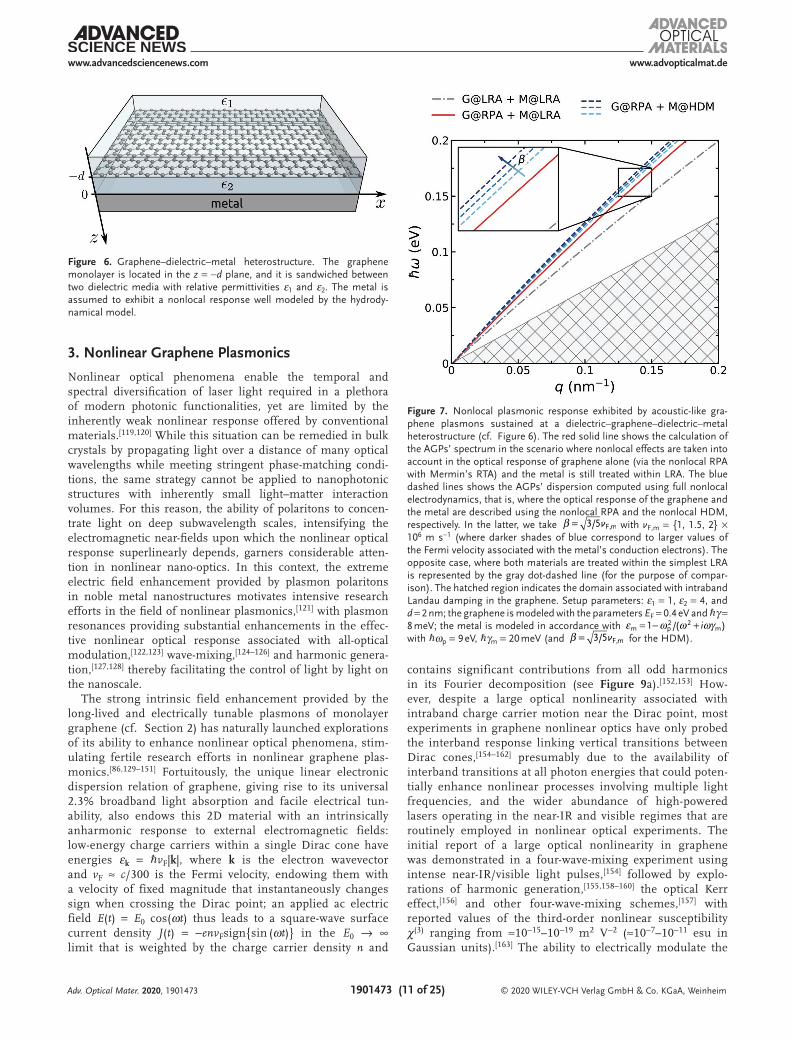
Figure 7 shows the AGPs’ spectrum computed using three different approaches: i) both the graphene and the metal are modeled within the LRA (this plays the role of a “base-line”), ii) the graphene electrodynamics are described within the non-local RPA, whereas the metal’s optical response is still treated within the LRA, and, finally, iii) the latter assumption is relaxed further and nonlocality in the metal is taken into account under the framework of the HDM. The results unambigu-ously demonstrate that the incorporation of nonlocality in the metal’s optical response imparts an additional blueshift to the AGPs’ dispersion. In particular, the magnitude of the blueshift
is proportional to the velocity of the hydrodynamic plasma pressure wave 3/5 F,mvβ = and inversely proportional to the metal’s plasma frequency (not shown; see ref. [105]).
Hence—and provided that all other parameters are well-known experimentally—we envision that one could use the theoretical framework outlined above in order to shed light about the metal’s nonlocal response, e.g., deducing the value of β by comparing the experimentally measured and the theoretical spectra.[104,105,109] A perhaps more appropriate reasoning, that squarely rests on the microscopic formalism of the Feibelman d-parameters,[110–112] is to establish a connec-tion between the value of β and the position of the centroid of the induced charge density with respect to the dielectric–metal interface (given by Red⊥, and where d⊥ is the main Feibelman d-parameter).
Next, in Figure 8, we examine the dependence of the non-local hydrodynamic blueshift on the graphene–metal separa-tion d. For the parameters considered in the figure (well within reach of current experimental capabilities[67,104]), the nonlocal response of the metal can lead to quite significant blueshifts of the AGPs’ dispersion for d ≲ 5 nm. This can be understood by realizing that AGPs attain increasingly larger wavevectors—and therefore are more sensitive to nonlocality in general—upon decreasing d.
Furthermore, for graphene–metal separations of only a few-nanometers, d becomes comparable to the penetration length of the electric field into the metal promoted by the smearing of the electronic density and concomitant “inward spill” of the screening charges due to nonlocality.[113–118] In particular, this notion has been exploited to theoretically describe plasmonic dimers by replacing the actual dimer separation d0 (which plays a similar role to the graphene–metal separation d in our geom-etry) by an “effective separation” deff ≠ d0 in order to capture (albeit only qualitatively) the above-noted nonlocal shift of the induced surface charges.[104,105,115,116]
Adv. Optical Mater. 2020, 1901473
Figure 5. Transition from the local to the nonlocal response regime by controlling the thickness d of the dielectric separating a graphene layer from a metal substrate. a) Pictorial representation of the graphene–dielectric–metal heterostructure under consideration. b) Plasmon velocity vp ∂ω/∂q as a function of the graphene–metal separation d (for a resonant frequency of ω/(2π) = 5 THz). c) Dispersion curves of graphene plasmons sup-ported by the graphene–dielectric–metal system for four different graphene–metal separations (indicated in the plot). The dispersion of conventional (“unscreened”) graphene plasmons is shown by the solid black line to facilitate the comparison and the interpretation of the results. Setup parameters:
(0) (0) 4.88dhBN hBNε ε ε= x z ,[67] ne = 1012 cm2 (which roughly amounts to EF = 0.117 eV, for vF = 106 m s−1); as in ref. [67], the metal is assumed to be well
approximated by a perfect electric conductor in the THz regime.
www.advancedsciencenews.com
© 2020 WILEY-VCH Verlag GmbH & Co. KGaA, Weinheim1901473 (11 of 25)
www.advopticalmat.de
3. Nonlinear Graphene Plasmonics
Nonlinear optical phenomena enable the temporal and spectral diversification of laser light required in a plethora of modern photonic functionalities, yet are limited by the inherently weak nonlinear response offered by conventional materials.[119,120] While this situation can be remedied in bulk crystals by propagating light over a distance of many optical wavelengths while meeting stringent phase-matching condi-tions, the same strategy cannot be applied to nanophotonic structures with inherently small light–matter interaction volumes. For this reason, the ability of polaritons to concen-trate light on deep subwavelength scales, intensifying the electromagnetic near-fields upon which the nonlinear optical response superlinearly depends, garners considerable atten-tion in nonlinear nano-optics. In this context, the extreme electric field enhancement provided by plasmon polaritons in noble metal nanostructures motivates intensive research efforts in the field of nonlinear plasmonics,[121] with plasmon resonances providing substantial enhancements in the effec-tive nonlinear optical response associated with all-optical modulation,[122,123] wave-mixing,[124–126] and harmonic genera-tion,[127,128] thereby facilitating the control of light by light on the nanoscale.
The strong intrinsic field enhancement provided by the long-lived and electrically tunable plasmons of monolayer graphene (cf. Section 2) has naturally launched explorations of its ability to enhance nonlinear optical phenomena, stim-ulating fertile research efforts in nonlinear graphene plas-monics.[86,129–151] Fortuitously, the unique linear electronic dispersion relation of graphene, giving rise to its universal 2.3% broadband light absorption and facile electrical tun-ability, also endows this 2D material with an intrinsically anharmonic response to external electromagnetic fields: low-energy charge carriers within a single Dirac cone have energies εk = ℏvF|k|, where k is the electron wavevector and vF ≈ c/300 is the Fermi velocity, endowing them with a velocity of fixed magnitude that instantaneously changes sign when crossing the Dirac point; an applied ac electric field E(t) = E0 cos(ωt) thus leads to a square-wave surface current density J(t) = −envFsign{sin (ωt)} in the E0 → ∞ limit that is weighted by the charge carrier density n and
contains significant contributions from all odd harmonics in its Fourier decomposition (see Figure 9a).[152,153] How-ever, despite a large optical nonlinearity associated with intraband charge carrier motion near the Dirac point, most experiments in graphene nonlinear optics have only probed the interband response linking vertical transitions between Dirac cones,[154–162] presumably due to the availability of interband transitions at all photon energies that could poten-tially enhance nonlinear processes involving multiple light frequencies, and the wider abundance of high-powered lasers operating in the near-IR and visible regimes that are routinely employed in nonlinear optical experiments. The initial report of a large optical nonlinearity in graphene was demonstrated in a four-wave-mixing experiment using intense near-IR/visible light pulses,[154] followed by explo-rations of harmonic generation,[155,158–160] the optical Kerr effect,[156] and other four-wave-mixing schemes,[157] with reported values of the third-order nonlinear susceptibility χ(3) ranging from ≈10−15–10−19 m2 V−2 (≈10−7–10−11 esu in Gaussian units).[163] The ability to electrically modulate the
Adv. Optical Mater. 2020, 1901473
Figure 6. Graphene–dielectric–metal heterostructure. The graphene monolayer is located in the z = −d plane, and it is sandwiched between two dielectric media with relative permittivities ε1 and ε2. The metal is assumed to exhibit a nonlocal response well modeled by the hydrody-namical model.
Figure 7. Nonlocal plasmonic response exhibited by acoustic-like gra-phene plasmons sustained at a dielectric–graphene–dielectric–metal heterostructure (cf. Figure 6). The red solid line shows the calculation of the AGPs’ spectrum in the scenario where nonlocal effects are taken into account in the optical response of graphene alone (via the nonlocal RPA with Mermin’s RTA) and the metal is still treated within LRA. The blue dashed lines shows the AGPs’ dispersion computed using full nonlocal electrodynamics, that is, where the optical response of the graphene and the metal are described using the nonlocal RPA and the nonlocal HDM, respectively. In the latter, we take 3/5 F,mvβ = with vF,m = {1, 1.5, 2} × 106 m s−1 (where darker shades of blue correspond to larger values of the Fermi velocity associated with the metal’s conduction electrons). The opposite case, where both materials are treated within the simplest LRA is represented by the gray dot-dashed line (for the purpose of compar-ison). The hatched region indicates the domain associated with intraband Landau damping in the graphene. Setup parameters: ε1 = 1, ε2 = 4, and d = 2 nm; the graphene is modeled with the parameters EF = 0.4 eV and ℏγ = 8 meV; the metal is modeled in accordance with 1 /( )m p
2 2mε ω ω ωγ= − + i
with ℏωp = 9 eV, ℏγm = 20 meV (and 3/5 F,mvβ = for the HDM).

www.advancedsciencenews.com
© 2020 WILEY-VCH Verlag GmbH & Co. KGaA, Weinheim1901473 (12 of 25)
www.advopticalmat.de
nonlinear optical response in graphene has recently been demonstrated,[161,162] along with high-harmonic generation (HHG) by the carbon monolayer when driven by intense terahertz[164] and mid-IR[165,166] light pulses.
Early theoretical ventures in nonlinear graphene plas-monics employed perturbation theory to reveal large second-harmonic[130] and Kerr-type optical nonlinearities[131] associated with the highly confined surface plasmon polari-tons hosted by extended graphene, which however cannot be directly launched by light from free space due to their large momenta. Nonlinear optical wave-mixing was later predicted to circumvent this limitation and enable the excita-tion of graphene plasmons with visible light impinging at angles such that a linear combinations of their frequency and in-plane optical momentum coincides with the plasmon dispersion curve lying well below the light line.[133,134] Fur-ther strengthening light–matter coupling to boost the intrin-sically large graphene nonlinearity, localized plasmons in graphene nanoresonators, concentrating light to volumes millions of times smaller than its corresponding free-space wavelength, are predicted to enable single-photon-level non-linear optical interactions,[132,138,149] optical bistability,[137] and intense nonlinear absorption.[136,147] These exciting prospects were explored in classical electrodynamic models of the nonlinear optical response associated with plasmons in gra-phene nanostructures, characterizing the optical response using the linear and nonlinear optical conductivities of extended graphene. In parallel, atomistic calculations of plasmons in nanostructured graphene, with the dynamics of electrons in tight-binding (TB) states governed by a single-particle density matrix in the self-consistent field
approximation—at the level of the RPA—revealed enormous nonlinear polarizabilities associated with harmonic genera-tion[86] and wave-mixing[135] processes (orders of magnitude above those produced by plasmons in similarly sized noble metal nanoparticles), confirming that the excellent nonlinear optical properties of graphene persist in its nanostructured form, and identifying the thresholds at which quantum finite-size effects emerge in structures with lateral size below ≈10 nm.[141] Time-domain simulations based on the TB+RPA method, which go beyond perturbation theory to enable the exploration of extreme nonlinear optical processes driven by intense ultrashort optical pulses, present further evidence of plasmonic enhancement in high-harmonic generation produced by doped graphene nanoribbons,[129] as we show in Figure 9b. We refer the interested reader to ref. [151] for a review on the nonlinear TB+RPA approach in nanostruc-tured graphene. For larger 2D nanostructures, the nonlinear optical response can be well-described by the theoretical description outlined in the following subsection, designed to model localized graphene plasmons but applicable to polaritons in other atomically thin materials characterized by 2D linear and nonlinear optical conductivities. Going beyond perturbation theory, we later discuss the regime of extreme nonlinear plasmonics, where intense optical pulses resonantly drive plasmon-enhanced saturable absorption and high-harmonic generation.
3.1. Analytical Description of Plasmon-Assisted Nonlinearity in Graphene Nanostructures
The nonlinear plasmonic response in graphene nanostruc-tures of ≳10 nm lateral size, i.e., beyond the threshold at which quantum finite-size effects play a non-negligible role,[80] can be described semi-analytically through the procedure introduced in ref. [143], which constitutes an extension of the electrostatic eigenmode expansion for the linear optical response outlined in ref. [66] (in a way reminiscent of the framework detailed in Section 2.2.1) to higher-order processes. In this model (pre-sented in this section in Gaussian units), the response associ-ated with a nonlinear optical process of order n and harmonic s [e.g., n = s = 3 for third-harmonic generation (THG)] to an external field Eexte−iωt + c.c. polarized in the ( , )x yrr
= plane of the graphene nanostructure, with geometry defined by the filling function ( )f rr
, is characterized by the induced dipole moment
i( ), ,
sdn s n spp rr jj rr
∫ω=
(13)
where the total current
,NL
, (1) ,jj jj EEσ= + ωn s n s
sn s
(14)
contains contributions from the intrinsic nonlinear current ,
NLjjn s
driven by the linear electric field
dfEE rr EE
rrrr rr
rr EE rr
∫σωε
= + ∇ ′− ′
∇′ ⋅ ′ ′ω( )i
| |( ) ( )1,1 ext
(1)1,1
(15)
Adv. Optical Mater. 2020, 1901473
Figure 8. Dependence of the nonlocal plasmonic response of acoustic-like graphene plasmons for varying graphene–metal separations d (indi-cated in the plot with matching colors). The response of graphene is evaluated at the level of the nonlocal RPA in all the cases shown here. As for the metal’s optical response, we consider two distinct models: the local response approximation (solid lines) and nonlocal hydrodynamic model (dashed lines). Setup parameters: same as in Figure 7 but with fixed 3/5 F,mvβ = , where vF,m = 1.4 × 10⁶ m s−1 (as in gold or silver).

www.advancedsciencenews.com
© 2020 WILEY-VCH Verlag GmbH & Co. KGaA, Weinheim1901473 (13 of 25)
www.advopticalmat.de
at the impinging light frequency ω and the current arising from the system’s linear response to the self-consistent non-linear field
( )i
| |( ), ,
s
dn s n sEE rrrr
rr rrjj rr
∫ω= ∇ ′
− ′∇′ ⋅ ′
(16)
at the generated frequency sω, while the form of the intrinsic nonlinear current
,NLjjn s
depends on the particular nonlinear pro-cess under consideration. For an inversion-symmetric graphene nanostructure, third-order processes constitute the leading con-tribution to the nonlinear response due to the inherent cen-trosymmetry of graphene’s hexagonal lattice; here we limit our discussion to THG and the optical Kerr nonlinearity, for which the associated currents are written as
( )NL3,3
3(3) 1,1 1,1 1,1jj EE EE EEσ= ⋅ω
(17)
2 | |NL3,1 (3) 1, 1 1,1 1,1 1,1 1,1 2jj EE EE EE EE EEσ ( )= ⋅ + ω
−
(18)
in terms of the local 2D nonlinear conductivities ( )snσ ω calculated
for extended graphene, obtained in the single-band approxi-mation by solving the semiclassical Boltzmann transport equation[143,152,167] or in quantum-mechanical approaches that incorporate effects both due to intraband and interband elec-tron processes.[163,168,169]
For a given 2D morphology and specific nonlinear optical process, the self-consistent solution of Equation (16) through the eigenmode expansion procedure detailed in ref. [143] yields
the nonlinear current jn,s entering the expression for the induced dipole in Equation (13). The analysis is simplified considerably by retaining only the dominant lowest-order dipolar plasmon mode in the expansion, choosing an inversion-symmetric geometry that suppresses any even-ordered nonlinear optical response, and considering normally impinging light; under these conditions, the nonvanishing linear and nonlinear polariz-abilities for a structure of characteristic size D are then given by
i1 ( )/
(1)2
(1)2
1
Dαω
σ ζη ω η
=−ω ω
(19)
Dαω
σ ξη ω η[ ]
=−
ω ωi
3 1 ( )/3(3)
2
3(3)
3,3
13
(20)
i
1 ( )/ | 1 ( )/ |(3)
2(3)
3,1
12
12
Dαω
σ ξη ω η η ω η[ ]
=− −
ω ω
(21)
where Dη ω σ εω= ω( ) i /(1) contains the dependence on the linear conductivity (1)σ ω and size, while the eigenvalue η1, the linear dipole coupling parameter ζ, and the nonlinear coupling parameters ξn,s are specific to the 2D geometry under consid-eration, and have been tabulated for various morphologies (e.g., disk, triangle, nanoribbon, etc.) in ref. [143].
While the above formalism is graphene-centered, it is impor-tant to recognize that the procedure is general to any 2D mate-rial characterized by isotropic, local conductivities. In the case of graphene, the third-order conductivities associated with
Adv. Optical Mater. 2020, 1901473
Figure 9. Nonlinear graphene optics and plasmon-assisted high-harmonic generation. a) The conical low-energy band structure of graphene (upper left) responds to a monochromatic electric field E(t) = E0 cos(ωt) by producing an induced current with a square-wave temporal profile in the E0 → ∞ limit, containing all odd-ordered harmonics in its Fourier spectrum; in contrast, a semiconducting crystal with parabolic charge carrier dispersion (upper right) responds to the same field harmonically at the driving frequency ω. b) The contour plot shows the simulated light emission (dipole acceleration) from a 20 nm wide graphene nanoribbon doped to EF = 0.4 eV when driven by a transverse-polarized normally incident light pulse as a function of the incident and emitted photon energies. The impinging pulse is characterized by a peak intensity of 1012 W m−2 and full width at half maximum (FWHM) duration of 100 fs. In the adjacent panels, the absorption cross-section normalized to the ribbon area is indicated along both axes of the contour plot by filled orange curves, with the emission produced upon resonant illumination of the nanoribbon plasmon plotted as a purple curve in the right panel, where the pulse is centered spectrally at ℏωp = 0.336 eV (i.e., at the energy indicated by the vertical dashed line in the contour). Adapted with permission.[129] Copyright 2017, Springer Nature.

www.advancedsciencenews.com
© 2020 WILEY-VCH Verlag GmbH & Co. KGaA, Weinheim1901473 (14 of 25)
www.advopticalmat.de
purely intraband charge carrier motion can be readily obtained from a perturbative solution of the Boltzmann transport equa-tion in the local approximation as (in Gaussian units)[143]
3i4
1( i )(2 i )(3 i )
3(3)
4F2
2F
1 1 1
e v
Eσ
π ω τ ω τ ω τ=
+ + +ω − − −
(22)
3i
4
1
(2 i )( )(3)
4F
2
2F
1 2 2
e v
Eσ
π ω τ ω τ= −
+ +ω − −
(23)
Analytical corrections to the above conductivities including interband contributions have been reported by Mikhailov,[169] and constitute an extension of the local RPA description of gra-phene to third-order.
In Figure 10, we employ the above procedure, incorpo-rating the third-order local RPA conductivities reported in ref. [169], to study plasmon-assisted third-order nonlinear optical processes in graphene nanoribbons characterized by a width D = 40 nm and EF = 1 eV doping, contrasting results of the analytical model (dashed curves) with those predicted in rigorous atomistic calculations of the linear and non-linear polarizabilities (solid curves). The four parameters η1 = −0.06873, ζ = 0.9428, ξ3,3 = −0.9415, and ξ3,1 = 3.093 asso-ciated with the lowest order ( j = 1) dipolar plasmon mode of the nanoribbon geometry already yield excellent agreement with the TB+RPA method, and can be improved by including higher-order modes.
3.2. Extreme Nonlinear Plasmonics
The strong electromagnetic field concentration provided by 2D plasmons in graphene reduces the light-intensity threshold for extreme nonlinear optical phenomena, arising when strong optical fields produce highly out-of-equilibrium electron dynamics that cannot be understood within a pertubative theo-retical framework. HHG is one such process, predicted to be particularly effective in highly doped, nanostructured graphene
due to the synergetic combination of plasmonic near-field enhancement and anharmonic intraband charge carrier motion near the Dirac point[129] (see Figure 9b). Plasmon-assisted HHG in graphene is however competing with its strong intrinsic satu-rable absorption,[170] which diminishes the in-plane plasmonic near-field enhancement in the material; the coherent saturable absorption is augmented by an incoherent saturation originating in the optical heating of electrons, which becomes substantial due to enhanced light absorption at the plasmon resonance.[145]
Several experimental investigations probing nonlinear plas-monic phenomena in both extended and nanostructured gra-phene resonators with intense pulsed laser fields are high-lighted in Figure 11. In particular, the electronic heating associ-ated with resonant excitation of plasmons constitutes an inco-herent but substantial source of optical nonlinearity that can be exploited to realize all-optical switching with relatively low-fluence pulses. This concept has been studied experimentally for propagating plasmons in extended graphene[171] and local-ized terahertz plasmons in ribbons.[140] Intense optical nonlin-earities associated with wave-mixing have also been observed in experiments, originally in extended graphene as a means to excite propagating plasmons directly from free space,[139] and later for nanoribbons in the near- and mid-infrared;[144] these studies also report a large effect attributed to the electronic heating produced by intense illumination.
The appeal of highly confined and actively tunable plasmons in graphene is partially offset by their limitation to mid-IR and lower frequencies, which presents a technological chal-lenge impeding its widespread application toward nonlinear nano-optical devices. With plasmon resonance frequencies in graphene nanostructures scaling as /FE Dω ∝ and practical considerations limiting the graphene doping level to EF ≈ 1 eV, one possibility to boost plasmon resonances to near-IR and visible frequencies consists in patterning graphene on very small length scales, possibly down to the molecular plas-monics regime, where graphene nanoislands are more akin to polycyclic aromatic hydrocarbons.[172] Interestingly, TB+RPA simulations for such graphene nanoislands down to sizes of only a few nano meters (in agreement with more sophis-ticated quantum chemistry simulations based on TDDFT)
Adv. Optical Mater. 2020, 1901473
Figure 10. Linear and nonlinear optical response of graphene nanoribbons. For a highly doped (EF = 1 eV) graphene nanoribbon of width D = 40 nm, we present a) the linear absorption cross-section 4 Im{ }/abs (1) cσ πω α= ω along with the nonlinear susceptibilities /( ) ( )
grd Dsn
snχ α=ω ω (normalizing the
polarizability per unit length by the ribbon width and graphene effective thickness dgr = 0.33 nm) for b) third-harmonic generation (n = s = 3) and c) the optical Kerr nonlinearity (n = 3, s = 1), comparing atomistic quantum-mechanical (QM) simulations for zigzag-edge-terminated ribbons (solid curves) with the classical (CL) analytical theory (broken curves); in the latter, dashed curves are obtained by limiting the modal expansion to the leading-order dipolar mode, while dash-dotted curves show the response including up to the first three dipole-active modes. Reproduced with permission.[143] Copyright 2018, American Physical Society.

www.advancedsciencenews.com
© 2020 WILEY-VCH Verlag GmbH & Co. KGaA, Weinheim1901473 (15 of 25)
www.advopticalmat.de
indicate that a large plasmon-assisted optical nonlinearity is maintained despite a breakdown of the Dirac cone electronic dispersion relation into discrete states separated by large energy gaps,[151] suggesting molecular self-assembly[173,174] as a path toward mid-IR nonlinear plasmonic devices. Graphene plasmons however constitute only one element within the broader suite of 2D polaritons that can undergo strong nonlinear optical interactions. As we discuss in the following section, exciton polaritons in TMDCs exhibit resonance ener-gies determined by the electronic bandgap of the material and the screened electron–hole interaction, and their strong cou-pling with proximal external plasmonic elements leads to the formation of hybridized exciton polaritons that have their own intrinsic optical nonlinearity.
4. Strong Light–Matter Interactions in Layered Transition Metal Dichalcogenides
The manipulation of light and matter is a foundational theme in photonics and plasmonics that enables applications in inte-grated light sources (conventional or quantum),[175] informa-tion processing,[175] as well as sensing and metrology.[176] The traditional approach is to utilize a photonic cavity to modify the electromagnetic environment of quantum light emitters such as natural atoms[177] or artificial emitters such as quantum dots based on semiconducting materials.[175] Depending on the strength of the coupling between the two subsystems we can distinguish two regimes, namely the weak and the strong-coupling regimes as explained in Section 4.1 and illustrated in Figure 12.
In the former regime, the rate of energy exchange between the emitter and the cavity is slower than any losses pertaining to the system’s constituents, and thus the light and matter states essentially remain as separate entities (albeit with modi-fied dynamics). In the weak coupling regime, the enhance-ment of the electromagnetic local density of states (LDOS) and of the field enhancement provided by the optical cavity can be used to increase the emission rate of an emitter: this behavior is known as the Purcell effect.[178–181] On the opposite end, that is, in the strong-coupling regime—where the rate of energy exchange between the emitter and the cavity is faster than any losses—the light and matter states hybridize to form new eigenstates simultaneously endowed with both light-like and matter-like character.[182] The hybrid nature of polaritons emerging in the strong-coupling regime offers many exciting opportunities not only for fundamental research[183] but also for quantum technologies such as photon blockades,[184] coherent quantum bit manipulation,[185] or new quantum light generation and thresholdless polaritonic lasers.[186] How-ever, in order to prevent detrimental dephasing processes in both the cavity and in the emitter, pioneering experimental works[187–189] have been carried out under cryogenic con-ditions,[188,189] thus limiting the development of scalable, application-oriented devices.
Over the last few years, there has been a growing interest in studying the strong-coupling regime using organic semi-conductors[189–192] and, more recently, atomically thin and 2D materials[34,193–202] as material platforms. Here, we give special emphasis to the latter. In particular, 2D materials like TMDCs can host excitons—electron–hole pairs bounded by the (screened) Coulomb interaction—that are stable at room
Adv. Optical Mater. 2020, 1901473
Figure 11. Experimental investigations in nonlinear graphene plasmonics. a) The left panel illustrates conceptually the prospect of optically exciting propagating plasmons in extended graphene through nonlinear wave-mixing (difference frequency generation), which can provide the momentum required to access the graphene plasmon dispersion curve lying well-outside the light line (red curve). In the right panel, the experimental signature of this process is observed through differential reflection as a function of the temporal overlap between pump and probe pulses. Adapted with per-mission.[139] Copyright 2016, Springer Nature. b) Pump–probe excitation of THz graphene plasmons in microribbon arrays reveals a strong transient nonlinear optical response associated with electronic heating. Reproduced with permission.[140] Copyright 2016, American Chemical Society. c) Infrared nanoimaging of hBN-encapsulated graphene reveals transient plasmons produced by femtosecond optical pump pulses, enabling real-space snapshots of the out-of-equilibrium electron dynamics. Adapted with permission.[171] Copyright 2016, Springer Nature. d) Experimental scheme to study plasmon-assisted nonlinear wave-mixing in graphene nanoribbons. Reproduced with permission.[144] Copyright 2018, American Chemical Society.

www.advancedsciencenews.com
© 2020 WILEY-VCH Verlag GmbH & Co. KGaA, Weinheim1901473 (16 of 25)
www.advopticalmat.de
temperature, thereby opening enticing prospects for exploring strong light–matter interactions under ambient conditions. Strong coupling at room temperature using dielectric cavities together with TMDCs[34] has been experimentally demonstrated, while similar systems such as metallic microcavities coupled to TMDCs[203] have also joined the race, exhibiting polaritonic split-tings as large as 100 meV.[204] Furthermore, Rabi-like splittings in excess of 100 meV have been achieved in systems utilizing plasmonic lattices and localized surface plasmons resonances (LSPRs) together with single inorganic quantum dots[205–208] or organic molecules,[209] such as J-aggregates,[210–213] and 2D materials.[195–202] At the time of writing, most of the reviews on strong coupling in nanophotonics[197,214–217] predominately cover previous works where the emitters are either conventional quantum dots or (in)organic molecules. Hence, herein we focus on reviewing the recent developments concerning strong light–matter interactions based on plasmonic resonances jointly with atomically thin materials, like TMDCs, as a growing number of experimental works have demonstrated sizable Rabi-like energy splittings[195–202,218] (e.g., as large as 175[201] and 190 meV[219]) using architectures based on few-layer and single-layer TMDCs. In the following, we provide an overview of the elementary principles describing strong coupling in a nanophotonics con-text. Next, we describe the basic optical properties of TMDCs and then review the most recent experimental investigations of strong coupling between excitons in atomically thin TMDCs and plasmonic resonances supported by metallic nanoparticles. In closing, we identify and discuss potential avenues for future investigations in this emerging and enticing field.
4.1. The Strong-Coupling Regime
Let us consider a plasmonic resonator—e.g., an individual metallic nanoparticle supporting a LSPR—in close proximity to an emitter such that there is significant overlap between the near-fields of the plasmonic cavity and of the emitter. If the emitter is well described by a point-like two-level system (Figure 12a), then the coupling energy follows from ( )0g EE rrµ= ⋅ , where µ is transition dipole moment associated with the tran-sition and ( )0EE rr is the electric field evaluated at the emitter’s position 0rr .[197,214,215,217] In this review, we shall consider that the “emitter” is represented by an excitonic resonance ascribed to the 2D TMDC (Figure 12b); in such a case, the previous expression cannot be employed directly and an explicit formula for the coupling energy is in general a nontrivial and onerous task (for a discussion about this predicament, see, for instance, ref. [220] and references therein). Notwithstanding, one may still in principle define an effective coupling (g geff herein) that could be inferred from experimental data.
In what follows, we treat the plasmon–exciton interac-tion semiclassically within the framework of the coupled-oscillator model,[34,194,217] wherein the coupling between the plasmon and the exciton is described by the non-Hermitian Hamiltonian
E
g
g
EE
i2 i
2
plpl
exex
α
β
α
β
−Γ
− Γ
=
±
±
±
(24)
Adv. Optical Mater. 2020, 1901473
Figure 12. Fundamentals of strong coupling in nanophotonics. a) Plasmonic open cavity, e.g., a plasmonic resonator of some arbitrary shape (here exemplified by a gold nanodisk for definiteness alone), characterized by a plasmon resonance of energy Epl and damping Γpl, placed in the vicinity of a point-like emitter (e.g., a canonical two-level system) characterized by a transition energy Eex, intrinsic linewidth Γex, and dipole moment µ. Here, the coherent exchange of energy between the two systems is described by the coupling strength g. b) Same plasmonic open cavity as in (a) but now near an atomically thin TMDC; the latter supports excitonic resonances that play the role previously assigned to the two-level system. The coupling between the two entities is now described by an effective coupling rate geff (that parameterizes the overall coupling due to an effective ensemble of excitons hosted by the 2D TMDC). c) Pictorial representation of the interaction-modified dynamics of the emitter (here a two-level system for simplicity). In the so-called weak coupling regime, defined by QR < 1 (see text), the emitter decay rate is enhanced (Purcell enhancement) without a substantial modifi-cation of the emitter (eigen)state. Conversely, in the strong-coupling regime, i.e., for QR > 1, the coupling is so large that it leads to the formation of two new eigenstates exhibiting hybrid emitter-cavity character(s), with energy being exchanged coherently at a rate governed by the Rabi frequency ΩR (which amounts to ℏΩR ≈ 2g in the low-loss regime).

www.advancedsciencenews.com
© 2020 WILEY-VCH Verlag GmbH & Co. KGaA, Weinheim1901473 (17 of 25)
www.advopticalmat.de
where Epl(ex) and Γpl(ex) are respectively the plasmon (exciton) resonant energy and associated linewidth, g denotes the cou-pling strength introduced above, and we introduce the ampli-tudes α and β describing the hybrid polaritonic states in terms of their plasmonic (α±) and excitonic (β±) constituents. The sys-tem’s eigenmodes can be straighforwardly calculated by diago-nalizing the Hamiltonian (24), which yields the following pair of eigenenergies
E E E
gi
1
2
i
4
1
24
2
pl ex pl ex
2pl ex
2
δ
( ) ( )
( )
= + − Γ + Γ
± + − Γ − Γ
±
(25)
where δ = Epl − Eex is the plasmon–exciton detuning. The eigen-values E± give rise to an energy spectrum divided into two branches: an upper-polariton branch (UPB; E+) and a lower-polariton branch (LPB; E−). The Rabi-like splitting, ER, is then defined as the energy difference between the UPB and LPB at zero detuning,[217] and reads
44
R2 pl ex
2
E g( )= −Γ − Γ
(26)
The criteria for strong coupling have been widely discussed in the literature,[182,197,217,221] and, broadly speaking, it is defined when the rate of coherent energy exchange exceeds any damping mechanisms (e.g., g ≫ Γpl, Γex). Although more than one criterion exists, a common approach to classify the strong coupling regime hinges on the fulfillment of the condition ER > (Γpl + Γex)/2 [provided that (4g)2 > (Γpl − Γex)2].[193,196,197,201,217] An alternative approach—which is particularly useful in the presence of large losses typical of plasmonic cavities—is to make use of the formalism introduced in ref. [222], and define the following figure-of-merit (FOM)
2R
R
pl ex
QE=
Γ + Γ (27)
As detailed in ref. [222], this quantity is a quality factor that essentially quantifies the number of temporal oscillations in the occupation numbers of the new eigenstates. As such, QR = 1 marks the onset of the strong-coupling regime: for QR < 1, that is, in the weak coupling regime, the original character of the modes is retained and the emitter population decays exponen-tially (Figure 12c; top row); on the other hand, in the strong coupling regime, marked by QR > 1, the occupation numbers of the hybrid eigenstates oscillate in time with a characteristic Rabi-like frequency of ΩR = ER/ℏ (Figure 12c; bottom row).
4.2. Excitons in Atomically Thin Semiconductors
In recent years, excitons—i.e., electron–hole pairs bounded through their mutual Coulomb interaction—in 2D materials like TMDCs have attracted a great deal of attention due to their singular optical properties.[223–225] These, to a great extent, reflect the presence of 2D excitons with large binding energies
(hundreds of meV), thereby making such collective excita-tions stable even at room temperature. This is in stark contrast with excitons in conventional bulk 3D semiconductors which typically possess binding energies of the order of k TB (where k T 26meVB at T = 300 K). The reason for this order-of-mag-nitude difference lies in inherently reduced screening in two dimensions.[223,224,226]
Furthermore, excitons in 2D TMDCs are not only stable at room temperature, but also host large (effective) dipole moments µ [195] oriented in-plane. Note that both of these fea-tures are instrumental to achieve the strong-coupling regime at room temperature.
As the low-energy physics of atomically thin TMDCs is well-described by an effective Dirac-like Hamiltonian with finite mass,[227,228] the valley degree of freedom can be used to manipulate the spin polarization of electrons—due to the siz-able spin-orbit coupling exhibited by such materials[223]—using circularly polarized light.[228–230] Pioneering experiments have shown that it is possible to inject excitons with highly polar-ized spins that could be utilized for valleytronics.[228–230] Con-versely, the valley polarization of these materials could also be exploited to coherently change the polarization state of the emitted light[231] or to steer the propagation direction of surface plasmon polaritons.[232,233]
Moreover, the intrinsic properties of 2D TMDCs can be actively tuned by doping via electrostatic gating. Crucially, this not only modifies the occupation number of electrons (holes) in the conduction (valence) bands, but also strongly influences the excitonic spectrum owing to the change in the screening dynamics. Additionally, doped 2D TMDCs can also host charged excitons (dubbed trions); these are excitonic complexes formed when a neutral exciton binds to another electron or hole, thereby forming a charged three-particle state.[223] These charged excitons are expected to play an important role in energy harvesting and in new optoelec-tronic devices.[234]
At low temperatures and for small doping, biexcitons (four-body states) can be formed and contribute to the optical response of 2D TMDCs.[235–237] Decaying biexcitons in TMDCs could be an interesting platform to generate entangled pairs of photons for quantum technologies such as quantum networks and quantum cryptography. On a more fundamental viewpoint, when the density of excitons is very high, new states of elec-tronic matter can be emerge such as dropletons[238] or Bose–Einstein condensates.[183,186,239]
Most of the experimental works exploiting 2D TMDCs as platforms for studying light–matter interactions in the strong-coupling regime have predominantly involved MoS2, WS2, or WSe2, presumably, because they are commercially available, can be synthesized by CVD methods, and their optical properties are stable under ambient conditions over a long period of time. Nevertheless, with the advances in nanofabrication methods[240] enabling the possibility to realize new atomically thin mate-rials with new properties, we anticipate the emergence of novel nanophotonic devices in the form of van der Waals heterostruc-tures[9,102] with functionalities going beyond the ones provided by the individual layers.
All the above-mentioned properties explain why 2D semicon-ducting TMDCs constitute exquisite architectures for exploring
Adv. Optical Mater. 2020, 1901473

www.advancedsciencenews.com
© 2020 WILEY-VCH Verlag GmbH & Co. KGaA, Weinheim1901473 (18 of 25)
www.advopticalmat.de
the rich physics of the strong-coupling regime (and, possibly, even in the ultrastrong-coupling regime[241]).
4.3. Strong Plasmon–Exciton Coupling with Plasmonic Cavities and TMDCs
The formation of exciton polaritons created by exploiting excitons in layered TMDCs in combination with photonic or plasmonic cavities has now been demonstrated by many groups,[34,193,195–202,211,213,243] signaling that the field has left its infant stage and has now reached adolescence. To illustrate this, in Figure 13 we provide a cursory overview of a number of hybrid metal–TMDCs systems exhibiting strong plasmon–exciton interactions. In most cases, the experimental setup con-sists in hybrid systems composed by atomically thin TMDCs in conjunction with plasmonic resonators, such as metallic nano-particles with various shapes,[195,196,199–201] nanoparticle-on-a-mirror (NPoM) geometries,[198,219,244] plasmonic crystals,[242,245] as well as plasmonic lattices.[204,246–248] A significant number of such plasmonic cavities are based on chemically grown metallic nanoparticles;[249,250] this is motivated by the high-quality (up to the single-crystalline level) and extremely low surface rough-ness presented by these nanoparticles, which naturally yield plasmonic resonances with smaller linewidths.
Typically, in order to reach the so-called strong-coupling regime one tries to maximize the coupling strength g while minimizing the overall damping mechanisms. As mentioned above, the latter can be achieved by employing highly crystal-line metal nanoparticles, whereas the former can be engineered
by maximizing the spatial overlap of the plasmonic mode with the 2D material hosting the excitonic resonance. Lastly, excitonic resonances exhibiting large oscillator strengths are naturally better candidates as platforms for strong coupling (in this regard, WS2 seems to be particularly well-suited for that end[225]).
As portrayed in Figure 13, substantial plasmon–exciton cou-pling has been achieved by combining different 2D TMDCs platforms with a plethora of plasmonic nanostructures such as nanorods, bipyramids, or nanodisks. Recently, it has been shown that one could improve the coupling strength (and thus obtain larger values of ER) by increasing the number of layers of TMDCs involved in the coupling process (Figure 13d).[198,200,201] Strikingly, the addition of a few more layers does not seem to significantly affect the excitonic resonance, despite modifying the material’s bandstructure and creating an indirect bandgap (instead the direct one exhibited in monolayers).[251] Hence, in this spirit, varying the number of layers incrementally could be a viable strategy to study the weak-to-strong coupling transition.
In Table 3, we have summarized some of the latest works exploring strong coupling in hybrid metal–TMDCs systems. Even though the list is of course not exhaustive, it clearly shows a vast breath of different metal–TMDCs platforms suitable for investigating strong-coupling in nanophotonics. In the table, we provide the parameters that characterize the plasmon–exciton interaction in each device, e.g., the amplitude of the measured Rabi-like splitting, along with the linewidths asso-ciated with the (uncoupled) plasmon and exciton resonances. These quantities then enable us to compute the FOM QR intro-duced in Equation (27) that quantifies the coupling strength.
Adv. Optical Mater. 2020, 1901473
Figure 13. Overview of the different hybrid metal–TMDC strutures used in recent experiments. a) Gold nanorods on WS2. Reproduced with permis-sion.[195] Copyright 2017, American Chemical Society. b) Metallic spheres-on-a-mirror with mono- and multilayer WSe2 in the gap. Adapted with permission.[198] Copyright 2017, Springer Nature. c) Plasmonic modes in silver nanotriangles coupled to excitons and trions in WS2. Reproduced with permission.[199] Copyright 2018, American Chemical Society. d) Gold bypiramids on mono- and multilayer WSe2. Adapted with permission.[200] Copyright 2018, American Chemical Society. e) Ultrathin gold nanodisks coupled to mono- and multilayer WS2. Reproduced with permission.[201] Copyright 2019, American Chemical Society. f) Dielectrically loaded plasmonic crystal in monocrystalline surfaces coupled to WSe2. Adapted with permission.[242] Copyright 2019, American Chemical Society.

www.advancedsciencenews.com
© 2020 WILEY-VCH Verlag GmbH & Co. KGaA, Weinheim1901473 (19 of 25)
www.advopticalmat.de
Firstly, notice that the energy splittings can range from about 18 meV[242] all the way up to values well above 150 meV.[201,219] In spite of this, most devices feature a FOM close to unity, i.e., QR ≈ 1, with many satisfy the strong coupling criterion QR > 1 (even though by a relatively small margin). Importantly, it is clear that the FOM can increase significantly when considering few-layer TMDCs (as opposed to its single-layer version).[200,201]
For comparison purposes with other platforms capable of achieving strong coupling at room temperature, we have also included in Table 3 the different parameters reported by Wersäll et al.[213] using LSPRs coupled to organic molecules as the “excitonic material”. Remarkably, they reach a FOM of 3.2, which constitutes the highest value reported so far for single plasmonic resonators coupled to emitters. This exceptionally large value could be explained by the fact that the J-aggregates used in this experiment entirely cover the silver nanotrian-gles, therefore maximizing the overlap of the plasmon mode with the exciton-supporting material. This is in contrast with the TMDCs-based setups that have been explored so far, where the TMDCs layer interacts mostly with only one fraction of the plasmon mode. Hence, we speculate on the possibility of increasing the overall coupling strength by, say, encapsulating such metallic nanoparticles with 2D TMDCs.
4.4. Perspectives on Strong Coupling
Since the first demonstration of strong coupling between LSPRs in metallic nanoparticles and excitons in 2D TMDCs, a growing number of experimental works have reported signatures of plasmon–exciton strong coupling probed by optical measure-ments. From the point of view of characterization techniques, many of the aforementioned experiments have used dark-field scattering spectroscopy methods[195,196,200,201] for determining the amplitude of the polariton anticrossing and infer from it wether the interaction is in the weak or strong coupling regime. How-ever, as it has been recently pointed out by a number of theo-retical[221,252] and experimental[205] works, the sole measurement of the scattering cross-section is not sufficient to unambiguously
conclude if the system is within strong-coupling regime. Indeed, the splitting observed in scattering measurements could simply be a consequence of plasmon-enhanced absorption or simply Fano-type physics.[252] Therefore, it is imperative to use other complementary characterization methods that can provide fur-ther insight about the plasmon–exciton coupling mechanism at work. For instance, examples of such methods are photolumi-nescence in the far-[205,213,219,253,254] and near-field[207,208] and/or spectroscopic methods enabling direct or indirect access to the absorption cross-section.[201,252] In addition, plasmon–exciton polaritons have also been observed using electron energy-loss-spectroscopy;[202] this technique opens enticing perspectives for probing plasmon–exciton interactions at the true nanom-eter scale. Furthermore, recent experimental works involving photoluminescence spectroscopy of LSPRs coupled to organic molecules[253] or excitons in TMDCs[198,219,254] have reported that most of the spontaneously emitted light originates from the LPB, with very little emission arising from the UPB. Neverthe-less, more investigations—e.g., using time-domain spectrosco-pies—are needed in order to obtain a deeper understanding of the dynamics in these systems.
Moreover, from the point of view of methods for fabricating 2D materials, there are many prospective systems waiting to be explored.[240] On the other hand, the recent discovery of superconductivity in graphene by simply twisting adjacent layers in bilayer graphene[7] hints at the possibility of tailoring many-body interactions involved in exciton formation by twisting TMDCs (dubbed “moiré excitons”).[255–258] This new degree of freedom, which is not present in conventional semi-conductors, opens the possibility to design novel exciton spe-cies that may in principle be optimally tailored in order to maxi-mize the coupling with electromagnetic modes.
Finally, in order to be suitable for quantum-based applica-tions, strong coupling achieved in hybrid metal–TMDC systems must necessarily pass a few experimental tests and demonstrate quantum coherence in the coupling between plasmon and exci-tons. In this regard, direct measurement in the time-domain of Rabi oscillations[259] would be an important step toward that end (though experimentally challenging due to the fast rate of
Adv. Optical Mater. 2020, 1901473
Table 3. Reported parameters from experimental works on individual localized surface plasmon resonances (LSPRs) interaction with atomically thin transition metal dichalcogenides (TMDCs) and corresponding calculated figure-of-merit (FOM) QR. For comparison, parameters and FOM from the experimental work of Wersäll et al.[213] with silver nanotriangles coupled to organic molecules are reported in the last columns. Abbreviations: nanocube-on-a-mirror (NCoM); room-temperature (RT); dielectrically loaded plasmonic cavity (DLPC).
Refs. LSPR TMDC # of layers ER [meV] Γpl [meV] Γex [meV] QR T [K]
[196] Ag nanorod WSe2 1 49.5 98 43 0.7 RT
[195] Au nanorods WS2 1 106 149 57 1.03 RT
[199] Ag nanotriangles WS2 1 120 190 20 1.14 RT
[200] Au bipyramids WSe2 8 101 110 63 1.17 RT
[244] NCoM WS2 1 145 220 50 1.07 RT
[245] Au nanoholes WS2 1 162 380 60 0.74 RT
[201] Au nanodisks WS2 7 175 170 44 1.64 RT
[242] Ag DLPC WSe2 1 18.2 7 7.5 2.51 4
[219] Ag NCoM MoS2 1 190 280 50 1.15 RT
[213] Ag nanotriangles J-aggregates N. A. 400 150 100 3.2 RT

www.advancedsciencenews.com
© 2020 WILEY-VCH Verlag GmbH & Co. KGaA, Weinheim1901473 (20 of 25)
www.advopticalmat.de
oscillation), as well as measuring the statistics and correlation functions of the emitted photons. Theoretical[260,261] and experi-mental[262] works have paved the way in that direction for sys-tems involving organic molecules interacting with LSPRs and still need to be demonstrated for 2D material-based devices.
5. Outlook
The advent of atomically thin materials—initiated and spear-headed by graphene—has opened enticing new routes for nanophotonics in two dimensions. In this review, we provide a hopefully representative sample of polaritons and light–matter interactions enabled by 2D polaritons (e.g., plasmon polaritons, exciton polaritons, phonon polaritons, etc.). Despite the fast-paced growth we have been witnessing over the last couple of years, it is not unfathomable to think that research in 2D nanophotonics has only scratched the surface, with a plethora of exciting possibilities over the horizon. While some of these possibilities are yet to be recognized, new avenues are already starting to be pursued. Examples of the latter are hyper-bolic[36,263] and chiral polaritonics,[233,264] using 2D polaritons for controlling the dynamics of emitters placed in the vicinity of a 2D material,[265] or the engineering of new flavors of polari-tons[29,30] (e.g., plasmon–exciton polaritons, plasmon–phonon polaritons, etc.). Other alluring research directions are 2D mate-rial-based topological photonics,[266,267] twist-polaritonics,[268–270] as well as transdimensional photonics[271] (i.e., the intermediate regime between the “strictly 3D” and the “strictly 2D” regime).
The strong field confinement and high tunability provided by 2D polaritons makes them an outstanding tool to control and study light–matter interactions at the nanoscale. In the light of the continuously increasing catalogue of 2D materials with diverse and complimentary optical and electronic properties, we anticipate that research in “flatland nanophotonics” will continue to flourish in the coming years, ultimately maturing in wide deployment of next-generation nanoscale optoelectronic devices.
AcknowledgementsThe Center for Nanostructured Graphene is sponsored by the Danish National Research Foundation (Project No. DNRF103). S.X. was supported by the Independent Research Fund Denmark (Project No. 9041-00333B). The Center for Nano Optics is supported by the University of Southern Denmark (SDU 2020 funding). J.D.C. and N.A.M. were supported by VILLUM Fonden (Grant No. 16498).
Conflict of InterestThe authors declare no conflict of interest.
Keywords2D materials, excitons, light–matter interaction, nanophotonics, plasmons, polaritons
Received: August 31, 2019Revised: October 29, 2019
Published online:
[1] K. S. Novoselov, A. K. Geim, S. V. Morozov, D. Jiang, Y. Zhang, S. V. Dubonos, I. V. Grigorieva, A. A. Firsov, Science 2004, 306, 666.
[2] K. S. Novoselov, D. Jiang, F. Schedin, T. J. Booth, V. V. Khotkevich, S. V. Morozov, A. K. Geim, Proc. Natl. Acad. Sci. USA 2005, 102, 10451.
[3] S. Tang, H. Wang, H. S. Wang, Q. Sun, X. Zhang, C. Cong, H. Xie, X. Liu, X. Zhou, F. Huang, X. Chen, T. Yu, F. Ding, X. Xie, M. Jiang, Nat. Commun. 2015, 6, 6499.
[4] X. Xu, Z. Zhang, L. Qiu, J. Zhuang, L. Zhang, H. Wang, C. Liao, H. Song, R. Qiao, P. Gao, Z. Hu, L. Liao, Z. Liao, D. Yu, E. Wang, F. Ding, H. Peng, K. Liu, Nat. Nanotechnol. 2016, 11, 930.
[5] T. Wu, X. Zhang, Q. Yuan, J. Xue, G. Lu, Z. Liu, H. Wang, H. Wang, F. Ding, Q. Yu, X. Xie, M. Jiang, Nat. Mater. 2016, 15, 43.
[6] X. Duan, C. Wang, J. C. Shaw, R. Cheng, Y. Chen, H. Li, X. Wu, Y. Tang, Q. Zhang, A. Pan, J. Jiang, R. Yu, Y. Huang, X. Duan, Nat. Nanotechnol. 2014, 9, 1024.
[7] Y. Cao, V. Fatemi, S. Fang, K. Watanabe, T. Taniguchi, E. Kaxiras, P. Jarillo-Herrero, Nature 2018, 556, 43.
[8] Y. Cao, V. Fatemi, A. Demir, S. Fang, S. L. Tomarken, J. Y. Luo, J. D. Sanchez-Yamagishi, K. Watanabe, T. Taniguchi, E. Kaxiras, R. C. Ashoori, P. Jarillo-Herrero, Nature 2018, 556, 80.
[9] K. S. Novoselov, A. Mishchenko, A. Carvalho, A. H. Castro Neto, Science 2016, 353, aac9439.
[10] F. Pizzocchero, L. Gammelgaard, B. S. Jessen, J. M. Caridad, L. Wang, J. Hone, P. Bøggild, T. J. Booth, Nat. Commun. 2016, 7, 11894.
[11] X. Yang, C. Cheng, Y. Wang, L. Qiu, D. Li, Science 2013, 341, 534.[12] W. Wu, L. Wang, Y. Li, F. Zhang, L. Lin, S. Niu, D. Chenet,
X. Zhang, Y. Hao, T. F. Heinz, J. Hone, Z. L. Wang, Nature 2014, 514, 470.
[13] M. Zhao, J. Zhang, N. Gao, P. Song, M. Bosman, B. Peng, B. Sun, C.-W. Qiu, Q.-H. Xu, Q. Bao, K. P. Loh, Adv. Mater. 2016, 28, 3138.
[14] B. Anasori, M. R. Lukatskaya, Y. Gogotsi, Nat. Rev. Mater. 2017, 2, 16098.
[15] F. Xia, H. Wang, D. Xiao, M. Dubey, A. Ramasubramaniam, Nat. Photonics 2014, 8, 899.
[16] F. Bonaccorso, Z. Sun, T. Hasan, A. C. Ferrari, Nat. Photonics 2010, 4, 611.
[17] M. Liu, X. Yin, E. Ulin-Avila, B. Geng, T. Zentgraf, L. Ju, F. Wang, X. Zhang, Nature 2011, 474, 64.
[18] C. T. Phare, Y.-H. D. Lee, J. Cardenas, M. Lipson, Nat. Photonics 2015, 9, 511.
[19] Y. Ding, X. Zhu, S. Xiao, H. Hu, L. H. Frandsen, N. A. Mortensen, K. Yvind, Nano Lett. 2015, 15, 4393.
[20] T. Mueller, F. Xia, P. Avouris, Nat. Photonics 2010, 4, 297.[21] Y. Ding, X. Guan, X. Zhu, H. Hu, S. I. Bozhevolnyi, L. K. Oxenlowe,
K. J. Jin, N. A. Mortensen, S. Xiao, Nanoscale 2017, 9, 15576.[22] Y. Ding, Z. Chen, X. Zhu, K. Yvind, J. Dong, M. Galili, H. Hu,
N. A. Mortensen, S. Xiao, L. K. Oxenløwe, Nanophotonics 2020, https://doi.org/10.1515/nanoph-2019-0167.
[23] D. Rodrigo, O. Limaj, D. Janner, D. Etezadi, F. J. García de Abajo, V. Pruneri, H. Altug, Science 2015, 349, 165.
[24] D. Rodrigo, A. Tittl, O. Limaj, F. J. García de Abajo, V. Pruneri, H. Altug, Light: Sci. Appl. 2017, 6, e16277.
[25] N. Dontschuk, A. Stacey, A. Tadich, K. J. Rietwyk, A. Schenk, M. T. Edmonds, O. Shimoni, C. I. Pakes, S. Prawer, J. Cervenka, Nat. Commun. 2015, 6, 6563.
[26] H. Hu, X. Yang, F. Zhai, D. Hu, R. Liu, K. Liu, Z. Sun, Q. Dai, Nat. Commun. 2016, 7, 12334.
[27] X. Chen, Y. J. Park, M. Kang, S.-K. Kang, J. Koo, S. M. Shinde, J. Shin, S. Jeon, G. Park, Y. Yan, M. R. MacEwan, W. Z. Ray, K.-M. Lee, J. A. Rogers, J.-H. Ahn, Nat. Commun. 2018, 9, 1690.
[28] H. Hu, X. Yang, X. Guo, K. Khaliji, S. R. Biswas, F. J. García de Abajo, T. Low, Z. Sun, Q. Dai, Nat. Commun. 2019, 10, 1131.
Adv. Optical Mater. 2020, 1901473

www.advancedsciencenews.com
© 2020 WILEY-VCH Verlag GmbH & Co. KGaA, Weinheim1901473 (21 of 25)
www.advopticalmat.de
[29] D. N. Basov, M. M. Fogler, F. J. García de Abajo, Science 2016, 354, aag1992.
[30] T. Low, A. Chaves, J. D. Caldwell, A. Kumar, N. X. Fang, P. Avouris, T. F. Heinz, F. Guinea, L. Martin-Moreno, F. Koppens, Nat. Mater. 2017, 16, 182.
[31] A. A. Balandin, D. L. Nika, Mater. Today 2012, 15, 266.[32] F. H. L. Koppens, D. E. Chang, F. J. García de Abajo, Nano Lett.
2011, 11, 3370.[33] L. Britnell, R. M. Ribeiro, A. Eckmann, R. Jalil, B. D. Belle,
A. Mishchenko, Y.-J. Kim, R. V. Gorbachev, T. Georgiou, S. V. Morozov, A. N. Grigorenko, A. K. Geim, C. Casiraghi, A. H. Castro Neto, K. S. Novoselov, Science 2013, 340, 1311.
[34] X. Liu, T. Galfsky, Z. Sun, F. Xia, E.-c. Lin, Y.-H. Lee, S. Kéna-Cohen, V. M. Menon, Nat. Photonics 2015, 9, 30.
[35] E. Yoxall, M. Schnell, A. Y. Nikitin, O. Txoperena, A. Woessner, M. B. Lundeberg, F. Casanova, L. E. Hueso, F. H. L. Koppens, R. Hillenbrand, Nat. Photonics 2015, 9, 674.
[36] S. Dai, Z. Fei, Q. Ma, A. S. Rodin, M. Wagner, A. S. McLeod, M. K. Liu, W. Gannett, W. Regan, K. Watanabe, T. Taniguchi, M. Thiemens, G. Dominguez, A. H. Castro Neto, A. Zettl, F. Keilmann, P. Jarillo-Herrero, M. M. Fogler, D. N. Basov, Science 2014, 343, 1125.
[37] P. Li, M. Lewin, A. V. Kretinin, J. D. Caldwell, K. S. Novoselov, T. Taniguchi, K. Watanabe, F. Gaussmann, T. Taubner, Nat. Commun. 2015, 6, 7507.
[38] A. Woessner, M. B. Lundeberg, Y. Gao, A. Principi, P. Alonso-González, M. Carrega, K. Watanabe, T. Taniguchi, G. Vignale, M. Polini, J. Hone, R. Hillenbrand, F. H. L. Koppens, Nat. Mater. 2015, 14, 421.
[39] M. Polini, F. H. L. Koppens, Nat. Mater. 2015, 14, 1187.[40] W. Ma, P. Alonso-Gonzalez, S. Li, A. Y. Nikitin, J. Yuan,
J. Martin-Sanchez, J. Taboada-Gutierrez, I. Amenabar, P. Li, S. Velez, C. Tollan, Z. Dai, Y. Zhang, S. Sriram, K. Kalantar-Zadeh, S.-T. Lee, R. Hillenbrand, Q. Bao, Nature 2018, 562, 557.
[41] P. A. D. Gonçalves, N. M. R. Peres, An Introduction to Graphene Plasmonics, World Scientific, Singapore 2016.
[42] F. J. García de Abajo, ACS Photonics 2014, 1, 135.[43] G. X. Ni, A. S. McLeod, Z. Sun, L. Wang, L. Xiong, K. W. Post,
S. S. Sunku, B.-Y. Jiang, J. Hone, C. R. Dean, M. M. Fogler, D. N. Basov, Nature 2018, 557, 530.
[44] S. Xiao, X. Zhu, B.-H. Li, N. A. Mortensen, Front. Phys. 2016, 11, 117801.
[45] A. H. Castro Neto, F. Guinea, N. M. R. Peres, K. S. Novoselov, A. K. Geim, Rev. Mod. Phys. 2009, 81, 109.
[46] K. Linghua, Y. Baorong, H. Xiwei, Plasma Sci. Technol. 2007, 9, 519.[47] D. G. Papageorgiou, I. A. Kinloch, R. J. Young, Prog. Mater. Sci.
2017, 90, 75.[48] T. Das, B. K. Sharma, A. K. Katiyar, J.-H. Ahn, J. Semicond. 2018,
39, 011007.[49] The relation between graphene’s Fermi energy, FE , and its elec-
tronic density, en , is given by F F eE v n π= . Typical values for the carrier density in doped graphene are 10 cme
11 2n = − to 10 cm13 2− [50,51], though values as high as 4 10 cme
14 2n = × − have been reported [52].
[50] L. Ju, B. Geng, J. Horng, C. Girit, M. Martin, Z. Hao, H. A. Bechtel, X. Liang, A. Zettl, Y. R. Shen, F. Wang, Nat. Nanotechnol. 2011, 6, 630.
[51] a) Z. Fei, A. S. Rodin, G. O. Andreev, W. Bao, A. S. McLeod, M. Wagner, L. M. Zhang, Z. Zhao, M. Thiemens, G. Dominguez, M. M. Fogler, A. H. C. Neto, C. N. Lau, F. Keilmann, D. N. Basov, Nature 2012, 487, 82; b) J. Chen, M. Badioli, P. Alonso-González, S. Thongrattanasiri, F. Huth, J. Osmond, M. Spasenovic, A. Centeno, A. Pesquera, P. Godignon, A. Z. Elorza, N. Camara, F. J. García de Abajo, R. Hillenbrand, F. H. L. Koppens, Nature 2012, 487, 77.
[52] D. K. Efetov, P. Kim, Phys. Rev. Lett. 2010, 105, 256805.[53] H. Liu, Y. Liu, D. Zhu, J. Mater. Chem. 2011, 21, 3335.[54] At the time of writing, several hundreds of 2D materials have been
identified. Most of them and their properties can be found in “2D materials databases” such as the ones provided in refs. [55,56].
[55] S. Haastrup, M. Strange, M. Pandey, T. Deilmann, P. S. Schmidt, N. F. Hinsche, M. N. Gjerding, D. Torelli, P. M. Larsen, A. C. Riis-Jensen, J. Gath, K. W. Jacobsen, J. J. Mortensen, T. Olsen, K. S. Thygesen, 2D Mater. 2018, 5, 042002.
[56] N. Mounet, M. Gibertini, P. Schwaller, D. Campi, A. Merkys, A. Marrazzo, T. Sohier, I. E. Castelli, A. Cepellotti, G. Pizzi, N. Marzari, Nat. Nanotechnol. 2018, 13, 246.
[57] N. D. Mermin, Phys. Rev. B 1970, 1, 2362.[58] J. Horng, C.-F. Chen, B. Geng, C. Girit, Y. Zhang, Z. Hao,
H. A. Bechtel, M. Martin, A. Zettl, M. F. Crommie, Y. R. Shen, F. Wang, Phys. Rev. B 2011, 83, 165113.
[59] L. A. Falkovsky, A. A. Varlamov, Eur. Phys. J. B 2007, 56, 281.[60] L. A. Falkovsky, S. S. Pershoguba, Phys. Rev. B 2007, 76, 153410.[61] B. Wunsch, T. Stauber, F. Sols, F. Guinea, New J. Phys. 2006, 8,
318.[62] E. H. Hwang, S. Das Sarma, Phys. Rev. B 2007, 75, 205418.[63] P. A. D. Gonçalves, E. J. C. Dias, S. Xiao, M. I. Vasilevskiy,
N. A. Mortensen, N. M. R. Peres, ACS Photonics 2016, 3, 2176.[64] P. A. D. Gonçalves, S. I. Bozhevolnyi, N. A. Mortensen,
N. M. R. Peres, Optica 2017, 4, 595.[65] P. A. D. Gonçalves, S. Xiao, N. M. R. Peres, N. A. Mortensen, ACS
Photonics 2017, 4, 3045.[66] R. Yu, J. D. Cox, J. R. M. Saavedra, F. J. García de Abajo,
ACS Photonics 2017, 4, 3106.[67] M. B. Lundeberg, Y. Gao, R. Asgari, C. Tan, B. Van Duppen,
M. Autore, P. Alonso-González, A. Woessner, K. Watanabe, T. Taniguchi, R. Hillenbrand, J. Hone, M. Polini, F. H. L. Koppens, Science 2017, 357, 187.
[68] F. Stern, Phys. Rev. Lett. 1967, 18, 546.[69] As detailed in the text, the nonretarded dispersion rela-
tion for plasmons supported by 2D electron systems can be generically written as 2 /Im ( )0ωε ε σ ω=q , assuming negli-gible loss. Hence, for a Drude-type 2D conductivity, this trans-
lates to 22D-plasmon0
ω πε ε= qD where D is the so-called Drude
weight. This quantity is defined via the Drude conductivity for an arbitrary 2D electron system, i.e., ( ) i
iDσ ω π ω γ= + .
Since the Drude weight of graphene, D / /G
2F
2 2F ee E e v nπ= = ,
is different than that of a parabolic 2DEG, D /2DEG2
e*e n mπ= ,
this leads to 2D plasmons whose dispersions exhibit different dependencies as a function of the electronic density, namely
, for plasmons in graphene
, for plasmons in a 2DEG2D-plasmon
1/2e1/4
2DEG1/2
e1/2
ω =
C q n
C q n
G , where, for the sake
of completeness, the constants in the previous expressions are
2G
2
0C e vFπε ε
= and
22DEG
2
0*C e
mε ε=
.[70] P. A. D. Gonçalves, E. J. C. Dias, Y. V. Bludov, N. M. R. Peres, Phys.
Rev. B 2016, 94, 195421.[71] J. Christensen, A. Manjavacas, S. Thongrattanasiri, F. H. L. Koppens,
F. J. García de Abajo, ACS Nano 2012, 6, 431.[72] H. Yan, T. Low, W. Zhu, Y. Wu, M. Freitag, X. Li, F. Guinea,
P. Avouris, F. Xia, Nat. Photonics 2013, 7, 394.[73] I. J. Luxmoore, C. H. Gan, P. Q. Liu, F. Valmorra, P. Li, J. Faist,
G. R. Nash, ACS Photonics 2014, 1, 1151.[74] C. Sorger, S. Preu, J. Schmidt, S. Winnerl, Y. V. Bludov,
N. M. R. Peres, M. I. Vasilevskiy, H. B. Weber, New J. Phys. 2015, 17, 053045.
[75] D. B. Farmer, P. Avouris, Y. Li, T. F. Heinz, S.-J. Han, ACS Photonics 2016, 3, 553.
Adv. Optical Mater. 2020, 1901473

www.advancedsciencenews.com
© 2020 WILEY-VCH Verlag GmbH & Co. KGaA, Weinheim1901473 (22 of 25)
www.advopticalmat.de
Adv. Optical Mater. 2020, 1901473
[76] X. Zhu, W. Yan, N. A. Mortensen, S. Xiao, Opt. Express 2013, 21, 3486.
[77] Y. Dai, X. Zhu, N. A. Mortensen, J. Zi, S. Xiao, J. Opt. 2015, 17, 065002.
[78] H. Yan, X. Li, B. Chandra, G. Tulevski, Y. Wu, M. Freitag, W. Zhu, P. Avouris, F. Xia, Nat. Nanotechnol. 2012, 7, 330.
[79] H. Yan, F. Xia, Z. Li, P. Avouris, New J. Phys. 2012, 14, 125001.[80] S. Thongrattanasiri, A. Manjavacas, F. J. García de Abajo, ACS
Nano 2012, 6, 1766.[81] Z. Fang, S. Thongrattanasiri, A. Schlather, Z. Liu, L. Ma, Y. Wang,
P. M. Ajayan, P. Nordlander, N. J. Halas, F. J. García de Abajo, ACS Nano 2013, 7, 2388.
[82] Z. Fang, Y. Wang, A. E. Schlather, Z. Liu, P. M. Ajayan, F. J. García de Abajo, P. Nordlander, X. Zhu, N. J. Halas, Nano Lett. 2014, 14, 299.
[83] X. Zhu, W. Wang, W. Yan, M. B. Larsen, P. Bøggild, T. G. Pedersen, S. Xiao, J. Zi, N. A. Mortensen, Nano Lett. 2014, 14, 2907.
[84] Z. Wang, T. Li, K. Almdal, N. A. Mortensen, S. Xiao, S. Ndoni, Opt. Lett. 2016, 41, 5345.
[85] W. Wang, S. Xiao, N. A. Mortensen, Phys. Rev. B 2016, 93, 165407.[86] J. D. Cox, F. J. García de Abajo, Nat. Commun. 2014, 5, 5725.[87] W. Wang, T. Christensen, A.-P. Jauho, K. S. Thygesen, M. Wubs,
N. A. Mortensen, Sci. Rep. 2015, 5, 9535.[88] K. Y. M. Yeung, J. Chee, H. Yoon, Y. Song, J. Kong, D. Ham, Nano
Lett. 2014, 14, 2479.[89] P. Q. Liu, F. Valmorra, C. Maissen, J. Faist, Optica 2015, 2, 135.[90] A. L. Fetter, Phys. Rev. B 1986, 33, 3717.[91] A. L. Fetter, Phys. Rev. B 1986, 33, 5221.[92] X. Xia, J. J. Quinn, Phys. Rev. B 1994, 50, 8032.[93] W. Wang, P. Apell, J. Kinaret, Phys. Rev. B 2011, 84, 085423.[94] W. Wang, S. P. Apell, J. M. Kinaret, Phys. Rev. B 2012, 86, 125450.[95] W. Wang, J. Phys.: Condens. Matter 2012, 24, 402202.[96] M. Abramowitz, I. A. Stegun, Handbook of Mathematical Functions:
With Formulas, Graphs, and Mathematical tables, Dover, New York 1972.
[97] V. A. Volkov, S. A. Mikhailov, Sov. Phys. JETP 1988, 67, 1639.[98] This fact was noted by Fetter [90], where he used the same method
for expanding the charge density instead of expanding the poten-tial. Naturally, such a formulation is tantamount—and ultimately equivalent—to the one described here. In any case, and perhaps more important for practical matters, we stress that the approach we follow here also admits a matrix with analytical matrix elements.
[99] S. Thongrattanasiri, F. H. L. Koppens, F. J. García de Abajo, Phys. Rev. Lett. 2012, 108, 047401.
[100] T. Christensen, W. Wang, A.-P. Jauho, M. Wubs, N. A. Mortensen, Phys. Rev. B 2014, 90, 241414(R).
[101] K. O. Wedel, N. A. Mortensen, K. S. Thygesen, M. Wubs, Phys. Rev. B 2018, 98, 155412.
[102] A. K. Geim, I. V. Grigorieva, Nature 2013, 499, 419.[103] P. Alonso-González, A. Y. Nikitin, Y. Gao, A. Woessner,
M. B. Lundeberg, A. Principi, N. Forcellini, W. Yan, S. Vélez, A. J. Huber, K. Watanabe, T. Taniguchi, F. Casanova, L. E. Hueso, M. Polini, J. Hone, F. H. L. Koppens, R. Hillenbrand, Nat. Nanotechnol. 2017, 12, 31.
[104] D. Alcaraz Iranzo, S. Nanot, E. J. C. Dias, I. Epstein, C. Peng, D. K. Efetov, M. B. Lundeberg, R. Parret, J. Osmond, J.-Y. Hong, J. Kong, D. R. Englund, N. M. R. Peres, F. H. L. Koppens, Science 2018, 360, 291.
[105] E. J. C. Dias, D. A. Iranzo, P. A. D. Gonçalves, Y. Hajati, Y. V. Bludov, A.-P. Jauho, N. A. Mortensen, F. H. L. Koppens, N. M. R. Peres, Phys. Rev. B 2018, 97, 245405.
[106] A. R. Echarri, J. D. Cox, F. J. García de Abajo, Optica 2019, 6, 630.
[107] S. Raza, S. I. Bozhevolnyi, M. Wubs, N. A. Mortensen, J. Phys.: Condens. Matter 2015, 27, 183204.
[108] If the dielectric media that encapsulate the graphene sheet are uni-axial
diag [ , , ]j jx
jx
jzε ε ε ε= (like, for instance, hBN) the corresponding
AGPs’ dispersion relation is nevertheless readily obtainable from Equation (12) upon making the following replacements: ε ε→j j
x and ( / ) 2
02κ ε ε ε→ −q kj j
xjz
jx for {1,2}j ∈ . This setting is considered in
Ref. [105], together with the hybridization of the acoustic-like gra-phene plasmons with the optical phonons in hBN.
[109] C. Ciracì, R. T. Hill, J. J. Mock, Y. Urzhumov, A. I. Fernández-Domínguez, S. A. Maier, J. B. Pendry, A. Chilkoti, D. R. Smith, Science 2012, 337, 1072.
[110] P. J. Feibelman, Prog. Surf. Sci. 1982, 12, 287.[111] T. Christensen, W. Yan, A.-P. Jauho, M. Soljacic, N. A. Mortensen,
Phys. Rev. Lett. 2017, 118, 157402.[112] P. A. D. Gonçalves, T. Christensen, N. Rivera, A.-P. Jauho,
N. A. Mortensen, M. Soljacic, Nat. Commun. 2020, https://doi.org/10.1038/s41467-019-13820-z.
[113] P. Ginzburg, A. V. Zayats, ACS Nano 2013, 7, 4334.[114] N. A. Mortensen, Photonics Nanostruct.: Fundam. Appl. 2013, 11,
303.[115] T. V. Teperik, P. Nordlander, J. Aizpurua, A. G. Borisov, Phys. Rev.
Lett. 2013, 110, 263901.[116] A. I. Fernández-Domínguez, P. Zhang, Y. Luo, S. A. Maier,
F. J. García-Vidal, J. B. Pendry, Phys. Rev. B 2012, 86, 241110.[117] W. Zhu, R. Esteban, A. G. Borisov, J. J. Baumberg, P. Nordlander,
H. J. Lezec, J. Aizpurua, K. B. Crozier, Nat. Commun. 2016, 7, 11495.
[118] G. Toscano, J. Straubel, A. Kwiatkowski, C. Rockstuhl, F. Evers, H. Xu, N. A. Mortensen, M. Wubs, Nat. Commun. 2015, 6, 7132.
[119] R. W. Boyd, Nonlinear Optics, Academic Press, Amsterdam 2008.[120] E. Garmire, Opt. Express 2013, 21, 30532.[121] M. Kauranen, A. V. Zayats, Nat. Photonics 2012, 6, 737.[122] C. Voisin, N. Del Fatti, D. Christofilos, F. Vallée, J. Phys. Chem. B
2001, 105, 2264.[123] M. Abb, P. Albella, J. Aizpurua, O. L. Muskens, Nano Lett. 2011,
11, 2457.[124] S. Palomba, L. Novotny, Phys. Rev. Lett. 2008, 101, 056802.[125] H. Harutyunyan, G. Volpe, R. Quidant, L. Novotny, Phys. Rev. Lett.
2012, 108, 217403.[126] Y. Zhang, F. Wen, Y.-R. Zhen, P. Nordlander, N. J. Halas, Proc.
Natl. Acad. Sci. USA 2013, 110, 9215.[127] J. Butet, P.-F. Brevet, O. J. F. Martin, ACS Nano 2015, 9,
10545.[128] A. Krasnok, M. Tymchenko, A. Alù, Mater. Today 2018, 21, 8.[129] J. D. Cox, A. Marini, F. J. García de Abajo, Nat. Commun. 2017, 8,
14380.[130] S. A. Mikhailov, Phys. Rev. B 2011, 84, 045432.[131] A. V. Gorbach, Phys. Rev. A 2013, 87, 013830.[132] M. Gullans, D. E. Chang, F. H. L. Koppens, F. J. García de Abajo,
M. D. Lukin, Phys. Rev. Lett. 2013, 111, 247401.[133] X. Yao, M. Tokman, A. Belyanin, Phys. Rev. Lett. 2014, 112, 055501.[134] J. Tao, Z. Dong, J. K. W. Yang, Q. J. Wang, Opt. Express 2015, 23,
7809.[135] J. D. Cox, F. J. García de Abajo, ACS Photonics 2015, 2, 306.[136] M. Jablan, D. E. Chang, Phys. Rev. Lett. 2015, 114, 236801.[137] T. Christensen, W. Yan, A.-P. Jauho, M. Wubs, N. A. Mortensen,
Phys. Rev. B 2015, 92, 121407(R).[138] M. T. Manzoni, I. Silveiro, F. J. García de Abajo, D. E. Chang, New
J. Phys. 2015, 17, 083031.[139] T. J. Constant, S. M. Hornett, D. E. Chang, E. Hendry, Nat. Phys.
2016, 12, 124.[140] M. M. Jadidi, J. C. König-Otto, S. Winnerl, A. B. Sushkov,
H. D. Drew, T. E. Murphy, M. Mittendorff, Nano Lett. 2016, 16, 2734.
[141] J. D. Cox, I. Silveiro, F. J. García de Abajo, ACS Nano 2016, 10, 1995.

www.advancedsciencenews.com
© 2020 WILEY-VCH Verlag GmbH & Co. KGaA, Weinheim1901473 (23 of 25)
www.advopticalmat.de
Adv. Optical Mater. 2020, 1901473
[142] H. Rostami, M. I. Katsnelson, M. Polini, Phys. Rev. B 2017, 95, 035416.
[143] J. D. Cox, R. Yu, F. J. García de Abajo, Phys. Rev. B 2017, 96, 045442.
[144] D. Kundys, B. V. Duppen, O. P. Marshall, F. Rodriguez, I. Torre, A. Tomadin, M. Polini, A. N. Grigorenko, Nano Lett. 2018, 18, 282.
[145] J. D. Cox, F. J. García de Abajo, Optica 2018, 5, 429.[146] J. D. Cox, F. J. García de Abajo, Phys. Rev. Lett. 2018, 121, 257403.[147] I. A. Calafell, J. D. Cox, M. Radonjic, J. R. M. Saavedra, F. J. García
de Abajo, L. A. Rozema, P. Walther, npj Quantum Inf. 2019, 5, 37.[148] T. Jiang, V. Kravtsov, M. Tokman, A. Belyanin, M. B. Raschke, Nat.
Nanotechnol. 2019, 14, 838.[149] J. D. Cox, F. J. García de Abajo, Nano Lett. 2019, 19, 3743.[150] C. Wolff, C. Tserkezis, N. A. Mortensen, New J. Phys. 2019, 21,
073046.[151] J. D. Cox, F. J. García de Abajo, Acc. Chem. Res. 2019, 52, 2536.[152] S. A. Mikhailov, Europhys. Lett. 2007, 79, 27002.[153] K. L. Ishikawa, Phys. Rev. B 2010, 82, 201402(R).[154] E. Hendry, P. J. Hale, J. Moger, A. K. Savchenko, S. A. Mikhailov,
Phys. Rev. Lett. 2010, 105, 097401.[155] A. Y. Bykov, T. V. Murzina, M. G. Rybin, E. D. Obraztsova, Phys.
Rev. B 2012, 85, 121413(R).[156] H. Zhang, S. Virally, Q. Bao, L. K. Ping, S. Massar, N. Godbout,
P. Kockaert, Opt. Lett. 2012, 37, 1856.[157] T. Gu, N. Petrone, J. F. McMillan, A. van der Zande, M. Yu,
G. Q. Lo, D. L. Kwong, J. Hone, C. W. Wong, Nat. Photonics 2012, 6, 554.
[158] N. Kumar, J. Kumar, C. Gerstenkorn, R. Wang, H.-Y. Chiu, A. L. Smirl, H. Zhao, Phys. Rev. B 2013, 87, 121406(R).
[159] S.-Y. Hong, J. I. Dadap, N. Petrone, P.-C. Yeh, J. Hone, R. M. Osgood Jr., Phys. Rev. X 2013, 3, 021014.
[160] Y. Q. An, J. E. Rowe, D. B. Dougherty, J. U. Lee, A. C. Diebold, Phys. Rev. B 2014, 89, 115310.
[161] T. Jiang, D. Huang, J. Cheng, X. Fan, Z. Zhang, Y. Shan, Y. Yi, Y. Dai, L. Shi, K. Liu, C. Zeng, J. Zi, J. E. Sipe, Y.-R. Shen, W.-T. Liu, S. Wu, Nat. Photonics 2018, 12, 430.
[162] G. Soavi, G. Wang, H. Rostami, D. G. Purdie, D. D. Fazio, T. Ma, B. Luo, J. Wang, A. K. Ott, D. Yoon, S. A. Bourelle, J. E. Muench, I. Goykhman, S. D. Conte, M. Celebrano, A. Tomadin, M. Polini, G. Cerullo, A. C. Ferrari, Nat. Nanotechnol. 2018, 13, 583.
[163] J. L. Cheng, N. Vermeulen, J. E. Sipe, New J. Phys. 2014, 16, 053104.[164] H. A. Hafez, S. Kovalev, J.-C. Deinert, Z. Mics, B. Green, N. Awari,
M. Chen, S. Germanskiy, U. Lehnert, J. Teichert, Z. Wang, K.-J. Tielrooij, Z. Liu, Z. Chen, A. Narita, K. Müllen, M. Bonn, M. Gensch, D. Turchinovich, Nature 2018, 561, 507.
[165] N. Yoshikawa, T. Tamaya, K. Tanaka, Science 2017, 356, 736.[166] M. Baudisch, A. Marini, J. D. Cox, T. Zhu, F. Silva, S. Teichmann,
M. Massicotte, F. Koppens, L. S. Levitov, F. J. García de Abajo, J. Biegert, Nat. Commun. 2018, 9, 1018.
[167] N. M. R. Peres, Y. V. Bludov, J. E. Santos, A.-P. Jauho, M. I. Vasilevskiy, Phys. Rev. B 2014, 90, 125425.
[168] J. L. Cheng, N. Vermeulen, J. E. Sipe, Phys. Rev. B 2015, 91, 235320.
[169] S. A. Mikhailov, Phys. Rev. B 2016, 93, 085403.[170] A. Marini, J. D. Cox, F. J. García de Abajo, Phys. Rev. B 2017, 95,
125408.[171] G. X. Ni, L. Wang, M. D. Goldflam, M. Wagner, Z. Fei,
A. S. McLeod, M. K. Liu, F. Keilmann, B. Özyilmaz, A. H. Castro Neto, J. Hone, M. M. Fogler, D. N. Basov, Nat. Photonics 2016, 10, 244.
[172] A. Lauchner, A. Schlather, A. Manjavacas, Y. Cui, M. J. McClain, G. J. Stec, F. J. García de Abajo, P. Nordlander, N. J. Halas, Nano Lett. 2015, 15, 6208.
[173] K. Müllen, ACS Nano 2014, 8, 6531.
[174] P. Ruffieux, S. Wang, B. Yang, C. Sánchez-Sánchez, J. Liu, T. Dienel, L. Talirz, P. Shinde, C. A. Pignedoli, D. Passerone, T. Dumslaff, X. Feng, K. Müllen, R. Fasel, Nature 2016, 531, 489.
[175] P. Lodahl, S. Mahmoodian, S. Stobbe, Rev. Mod. Phys. 2015, 87, 347.
[176] X.-L. Chu, S. Götzinger, V. Sandoghdar, Nat. Photonics 2017, 11, 58.
[177] J.-M. Raimond, M. Brune, S. Haroche, Rev. Mod. Phys. 2001, 73, 565.
[178] M. Pelton, Nat. Photonics 2015, 9, 427.[179] K. J. Russell, T.-L. Liu, S. Cui, E. L. Hu, Nat. Photonics 2012,
6, 459.[180] G. M. Akselrod, C. Argyropoulos, T. B. Hoang, C. Ciracì, C. Fang,
J. Huang, D. R. Smith, M. H. Mikkelsen, Nat. Photonics 2014, 8, 835.
[181] I. M. Palstra, H. M. Doeleman, A. F. Koenderink, Nanophotonics 2019, 8, 1513.
[182] G. Khitrova, H. M. Gibbs, M. Kira, S. W. Koch, A. Scherer, Nat. Phys. 2006, 2, 81.
[183] I. Carusotto, C. Ciuti, Rev. Mod. Phys. 2013, 85, 299.[184] D. E. Chang, A. S. Sørensen, E. A. Demler, M. D. Lukin, Nat. Phys.
2007, 3, 807.[185] A. Wallraff, D. I. Schuster, A. Blais, L. Frunzio, R.-S. Huang,
J. Majer, S. Kumar, S. M. Girvin, R. J. Schoelkopf, Nature 2004, 431, 162.
[186] D. Sanvitto, S. Kéna-Cohen, Nat. Mater. 2016, 15, 1061.[187] Y. Kaluzny, P. Goy, M. Gross, J. Raimond, S. Haroche, Phys. Rev.
Lett. 1983, 51, 1175.[188] C. Weisbuch, M. Nishioka, A. Ishikawa, Y. Arakawa, Phys. Rev. Lett.
1992, 69, 3314.[189] D. G. Lidzey, D. Bradley, M. Skolnick, T. Virgili, S. Walker,
D. Whittaker, Nature 1998, 395, 53.[190] J. Bellessa, C. Bonnand, J. C. Plenet, J. Mugnier, Phys. Rev. Lett.
2004, 93, 036404.[191] S. Kéna-Cohen, S. Forrest, Nat. Photonics 2010, 4, 371.[192] E. Orgiu, J. George, J. Hutchison, E. Devaux, J. Dayen,
B. Doudin, F. Stellacci, C. Genet, J. Schachenmayer, C. Genes, G. Pupillo, P. Samorì, T. W. Ebbesen, Nat. Mater. 2015, 14, 1123.
[193] A. Krasnok, S. Lepeshov, A. Alú, Opt. Express 2018, 26, 15972.
[194] P. A. D. Gonçalves, L. P. Bertelsen, S. Xiao, N. A. Mortensen, Phys. Rev. B 2018, 97, 041402(R).
[195] J. Wen, H. Wang, W. Wang, Z. Deng, C. Zhuang, Y. Zhang, F. Liu, J. She, J. Chen, H. Chen, S. Deng, N. Xu, Nano Lett. 2017, 17, 4689.
[196] D. Zheng, S. Zhang, Q. Deng, M. Kang, P. Nordlander, H. Xu, Nano Lett. 2017, 17, 3809.
[197] D. G. Baranov, M. Wersäll, J. Cuadra, T. J. Antosiewicz, T. Shegai, ACS Photonics 2017, 5, 24.
[198] M.-E. Kleemann, R. Chikkaraddy, E. M. Alexeev, D. Kos, C. Carnegie, W. Deacon, A. C. de Pury, C. Große, B. de Nijs, J. Mertens, A. I. Tartakovskii, J. J. Baumberg, Nat. Commun. 2017, 8, 1296.
[199] J. Cuadra, D. G. Baranov, M. Wersäll, R. Verre, T. J. Antosiewicz, T. Shegai, Nano Lett. 2018, 18, 1777.
[200] M. Stührenberg, B. Munkhbat, D. G. Baranov, J. Cuadra, A. B. Yankovich, T. J. Antosiewicz, E. Olsson, T. Shegai, Nano Lett. 2018, 18, 5938.
[201] M. Geisler, X. Cui, J. Wang, T. Rindzevicius, L. Gammelgaard, B. S. Jessen, P. A. D. Gonçalves, F. Todisco, P. Bøggild, A. Boisen, M. Wubs, N. A. Mortensen, S. Xiao, N. Stenger, ACS Photonics 2019, 6, 994.

www.advancedsciencenews.com
© 2020 WILEY-VCH Verlag GmbH & Co. KGaA, Weinheim1901473 (24 of 25)
www.advopticalmat.de
Adv. Optical Mater. 2020, 1901473
[202] A. B. Yankovich, B. Munkhbat, D. G. Baranov, J. Cuadra, E. Olsén, H. Lourenço-Martins, L. H. Tizei, M. Kociak, E. Olsson, T. Shegai, Nano Lett. 2019, 19, 8171.
[203] B. Chakraborty, J. Gu, Z. Sun, M. Khatoniar, R. Bushati, A. L. Boehmke, R. Koots, V. M. Menon, Nano Lett. 2018, 18, 6455.
[204] S. Wang, S. Li, T. Chervy, A. Shalabney, S. Azzini, E. Orgiu, J. A. Hutchison, C. Genet, P. Samorì, T. W. Ebbesen, Nano Lett. 2016, 16, 4368.
[205] H. Leng, B. Szychowski, M.-C. Daniel, M. Pelton, Nat. Commun. 2018, 9, 4012.
[206] K. Santhosh, O. Bitton, L. Chuntonov, G. Haran, Nat. Commun. 2016, 7, 11823.
[207] H. Groß, J. M. Hamm, T. Tufarelli, O. Hess, B. Hecht, Sci. Adv. 2018, 4, eaar4906.
[208] K.-D. Park, M. A. May, H. Leng, J. Wang, J. A. Kropp, T. Gougousi, M. Pelton, M. B. Raschke, Sci. Adv. 2019, 5, eaav5931.
[209] R. Chikkaraddy, B. De Nijs, F. Benz, S. J. Barrow, O. A. Scherman, E. Rosta, A. Demetriadou, P. Fox, O. Hess, J. J. Baumberg, Nature 2016, 535, 127.
[210] A. E. Schlather, N. Large, A. S. Urban, P. Nordlander, N. J. Halas, Nano Lett. 2013, 13, 3281.
[211] A. I. Väkeväinen, R. J. Moerland, H. T. Rekola, A.-P. Eskelinen, J.-P. Martikainen, D.-H. Kim, P. Törmä, Nano Lett. 2014, 14, 1721.
[212] G. Zengin, M. Wersäll, S. Nilsson, T. J. Antosiewicz, M. Käll, T. Shegai, Phys. Rev. Lett. 2015, 114, 157401.
[213] M. Wersäll, J. Cuadra, T. J. Antosiewicz, S. Balci, T. Shegai, Nano Lett. 2016, 17, 551.
[214] J. T. Hugall, A. Singh, N. F. van Hulst, ACS Photonics 2018, 5, 43.[215] F. Marquier, C. Sauvan, J.-J. Greffet, ACS Photonics 2017, 4, 2091.[216] P. Vasa, C. Lienau, ACS Photonics 2017, 5, 2.[217] P. Törmä, W. L. Barnes, Rep. Prog. Phys. 2014, 78, 013901.[218] X. Zhang, C. De-Eknamkul, J. Gu, A. L. Boehmke, V. M. Menon,
J. Khurgin, E. Cubukcu, Nat. Nanotechnol. 2019, 14, 844.[219] S. Hou, L. Y. Tobing, X. Wang, Z. Xie, J. Yu, J. Zhou, D. Zhang,
C. Dang, P. Coquet, B. K. Tay, M. D. Birowosuto, E. H. T. Teo, H. Wang, Adv. Opt. Mater. 2019, 7, 1900857.
[220] C. Tserkezis, A. Fernández-Domínguez, P. A. D. Gonçalves, F. Todisco, J. Cox, K. Busch, N. Stenger, S. Bozhevolnyi, N. A. Mortensen, C. Wolff, arXiv:1907.02605, 2019.
[221] M. Pelton, S. D. Storm, H. Leng, Nanoscale 2019, 11, 14540.[222] F. Todisco, R. Malureanu, C. Wolff, P. A. D. Gonçalves,
A. S. Roberts, N. A. Mortensen, C. Tserkezis, arXiv:1906.09898, 2019.
[223] G. Wang, A. Chernikov, M. M. Glazov, T. F. Heinz, X. Marie, T. Amand, B. Urbaszek, Rev. Mod. Phys. 2018, 90, 021001.
[224] K. S. Thygesen, 2D Mater. 2017, 4, 022004.[225] Y. Li, A. Chernikov, X. Zhang, A. Rigosi, H. M. Hill,
A. M. van der Zande, D. A. Chenet, E.-M. Shih, J. Hone, T. F. Heinz, Phys. Rev. B 2014, 90, 205422.
[226] A. Chernikov, T. C. Berkelbach, H. M. Hill, A. Rigosi, Y. Li, O. B. Aslan, D. R. Reichman, M. S. Hybertsen, T. F. Heinz, Phys. Rev. Lett. 2014, 113, 076802.
[227] A. J. Chaves, R. M. Ribeiro, T. Frederico, N. M. R. Peres, 2D Mater. 2017, 4, 025086.
[228] D. Xiao, G.-B. Liu, W. Feng, X. Xu, W. Yao, Phys. Rev. Lett. 2012, 108, 196802.
[229] H. Zeng, J. Dai, W. Yao, D. Xiao, X. Cui, Nat. Nanotechnol. 2012, 7, 490.
[230] T. Cao, G. Wang, W. Han, H. Ye, C. Zhu, J. Shi, Q. Niu, P. Tan, E. Wang, B. Liu, J. Feing, Nat. Commun. 2012, 3, 887.
[231] A. M. Jones, H. Yu, N. J. Ghimire, S. Wu, G. Aivazian, J. S. Ross, B. Zhao, J. Yan, D. G. Mandrus, D. Xiao, W. Yao, X. X, Nat. Nanotechnol. 2013, 8, 634.
[232] S.-H. Gong, F. Alpeggiani, B. Sciacca, E. C. Garnett, L. Kuipers, Science 2018, 359, 443.
[233] T. Chervy, S. Azzini, E. Lorchat, S. Wang, Y. Gorodetski, J. A. Hutchison, S. Berciaud, T. W. Ebbesen, C. Genet, ACS Photo nics 2018, 5, 1281.
[234] J. S. Ross, P. Klement, A. M. Jones, N. J. Ghimire, J. Yan, D. Mandrus, T. Taniguchi, K. Watanabe, K. Kitamura, W. Yao, D. H. Cobden, X. Xu, Nat. Nanotechnol. 2014, 9, 268.
[235] Y. You, X.-X. Zhang, T. C. Berkelbach, M. S. Hybertsen, D. R. Reichman, T. F. Heinz, Nat. Phys. 2015, 11, 477.
[236] A. Steinhoff, M. Florian, A. Singh, K. Tran, M. Kolarczik, S. Helmrich, A. W. Achtstein, U. Woggon, N. Owschimikow, F. Jahnke, X. Li, Nat. Phys. 2018, 14, 1199.
[237] J. Pei, J. Yang, X. Wang, F. Wang, S. Mokkapati, T. Lü, J.-C. Zheng, Q. Qin, D. Neshev, H. H. Tan, C. Jagadish, Y. Lu, ACS Nano 2017, 11, 7468.
[238] A. Almand-Hunter, H. Li, S. Cundiff, M. Mootz, M. Kira, S. W. Koch, Nature 2014, 506, 471.
[239] H. Deng, H. Haug, Y. Yamamoto, Rev. Mod. Phys. 2010, 82, 1489.[240] A. Shivayogimath, J. D. Thomsen, D. M. Mackenzie, M. Geisler,
R.-M. Stan, A. J. Holt, M. Bianchi, A. Crovetto, P. R. Whelan, A. Carvalho, A. H. Castro Neto, P. Hofmann, S. Stenger, P. Bøggild, T. J. Booth, Nat. Commun. 2019, 10, 2957.
[241] A. F. Kockum, A. Miranowicz, S. D. Liberato, S. Savasta, F. Nori, Nat. Rev. Phys. 2019, 1, 19.
[242] A. M. Dibos, Y. Zhou, L. A. Jauregui, G. Scuri, D. S. Wild, A. A. High, T. Taniguchi, K. Watanabe, M. D. Lukin, P. Kim, H. Park, Nano Lett. 2019, 19, 3543.
[243] L. C. Flatten, Z. He, D. M. Coles, A. A. P. Trichet, A. W. Powell, R. A. Taylor, J. H. Warner, J. M. Smith, Sci. Rep. 2016, 6, 33134.
[244] X. Han, K. Wang, X. Xing, M. Wang, P. Lu, ACS Photonics 2018, 5, 3970.
[245] X. Chen, H. Wang, N.-S. Xu, H. Chen, S. Deng, Appl. Mater. Today 2019, 15, 145.
[246] B. Lee, J. Park, G. H. Han, H.-S. Ee, C. H. Naylor, W. Liu, A. C. Johnson, R. Agarwal, Nano Lett. 2015, 15, 3646.
[247] W. Liu, B. Lee, C. H. Naylor, H.-S. Ee, J. Park, A. T. C. Johnson, R. Agarwal, Nano Lett. 2016, 16, 1262.
[248] B. Lee, W. Liu, C. H. Naylor, J. Park, S. C. Malek, J. S. Berger, A. T. C. Johnson, R. Agarwal, Nano Lett. 2017, 17, 4541.
[249] X. Lu, M. Rycenga, S. E. Skrabalak, B. Wiley, Y. Xia, Annu. Rev. Phys. Chem. 2009, 60, 167.
[250] F. Qin, T. Zhao, R. Jiang, N. Jiang, Q. Ruan, J. Wang, L.-D. Sun, C.-H. Yan, H.-Q. Lin, Adv. Opt. Mater. 2016, 4, 76.
[251] H. Zeng, G.-B. Liu, J. Dai, Y. Yan, B. Zhu, R. He, L. Xie, S. Xu, X. Chen, W. Yao, X. Cui, Sci. Rep. 2013, 3, 1608.
[252] T. J. Antosiewicz, S. P. Apell, T. Shegai, ACS Photonics 2014, 1, 454.[253] M. Wersäll, B. Munkhbat, D. G. Baranov, F. Herrera, J. Cao,
T. J. Antosiewicz, T. Shegai, ACS Photonics 2019, 6, 2570.[254] L. Liu, L. Y. Tobing, X. Yu, J. Tong, B. Qiang,
A. I. Fernández-Domínguez, F. J. Garcia-Vidal, D. H. Zhang, Q. J. Wang, Y. Luo, Adv. Opt. Mater. 2019, 7, 1901002.
[255] K. Tran, G. Moody, F. Wu, X. Lu, J. Choi, K. Kim, A. Rai, D. A. Sanchez, J. Quan, A. Singh, J. Embley, A. Zepeda, M. Campbell, T. Autry, T. Taniguchi, K. Watanabe, N. Lu, S. K. Banerjee, K. L. Silverman, S. Kim, E. Tutuc, L. Yang, A. H. MacDonald, X. Li, Nature 2019, 567, 71.
[256] K. L. Seyler, P. Rivera, H. Yu, N. P. Wilson, E. L. Ray, D. G. Mandrus, J. Yan, W. Yao, X. Xu, Nature 2019, 567, 66.
[257] C. Jin, E. C. Regan, A. Yan, M. I. B. Utama, D. Wang, S. Zhao, Y. Qin, S. Yang, Z. Zheng, S. Shi, K. Watanabe, T. Taniguchi, S. Tongay, A. Zettl, F. Wang, Nature 2019, 567, 76.
[258] E. M. Alexeev, D. A. Ruiz-Tijerina, M. Danovich, M. J. Hamer, D. J. Terry, P. K. Nayak, S. Ahn, S. Pak, J. Lee, J. I. Sohn, M. R. Molas, M. Koperski, K. Watanabe, T. Taniguchi, K. S. Novoselov, R. V. Gorbachev, H. S. Shin, V. I. Fal’ko, A. I. Tartakovskii, Nature 2019, 567, 81.

www.advancedsciencenews.com
© 2020 WILEY-VCH Verlag GmbH & Co. KGaA, Weinheim1901473 (25 of 25)
www.advopticalmat.de
Adv. Optical Mater. 2020, 1901473
[259] P. Vasa, W. Wang, R. Pomraenke, M. Lammers, M. Maiuri, C. Manzoni, G. Cerullo, C. Lienau, Nat. Photonics 2013, 7, 128.
[260] A. I. Fernández-Domínguez, S. I. Bozhevolnyi, N. A. Mortensen, ACS Photonics 2018, 5, 3447.
[261] R. Sáez-Blázquez, J. Feist, A. Fernández-Domínguez, F. García-Vidal, Optica 2017, 4, 1363.
[262] O. S. Ojambati, R. Chikkaraddy, W. D. Deacon, M. Horton, D. Kos, V. A. Turek, U. F. Keyser, J. J. Baumberg, Nat. Commun. 2019, 10, 1049.
[263] A. Nemilentsau, T. Low, G. Hanson, Phys. Rev. Lett. 2016, 116, 066804.
[264] J. C. W. Song, M. S. Rudner, Proc. Natl. Acad. Sci. USA 2016, 113, 4658.[265] N. Rivera, I. Kaminer, B. Zhen, J. D. Joannopoulos, M. Soljacic,
Science 2016, 353, 263.
[266] L. Ju, Z. Shi, N. Nair, Y. Lv, C. Jin, J. Velasco, C. Ojeda-Aristizabal, H. A. Bechtel, M. C. Martin, A. Zettl, J. Analytis, F. Wang, Nature 2015, 520, 650.
[267] A. B. Khanikaev, G. Shvets, Nat. Photonics 2017, 11, 763.[268] F. Hu, S. R. Das, Y. Luan, T.-F. Chung, Y. P. Chen, Z. Fei, Phys. Rev.
Lett. 2017, 119, 247402.[269] C. Lewandowski, L. Levitov, Proc. Natl. Acad. Sci. U SA 2019, 116,
20869.[270] N. C. Hesp, I. Torre, D. Rodan-Legrain, P. Novelli, Y. Cao, S. Carr,
S. Fang, P. Stepanov, D. Barcons-Ruiz, H. Herzig-Sheinfux, K. Watanabe, T. Taniguchi, D. K. Efetov, E. Kaxiras, P. Jarillo-Herrero, M. Polini, F. H. Koppens, arXiv:1910.07893, 2019.
[271] A. Boltasseva, V. M. Shalaev, ACS Photonics 2019, 6, 1.