structural analysis of nanomaterials using electron …maud/maud2015/maud2015-philippe.pdfmaud...
TRANSCRIPT
MAUD School 2015
Structural Analysis of Nanomaterialsusing Electron Diffraction
Philippe BOULLAYCristallographie et Sciences des Matériaux – CRISMAT UMR 6508 CNRS – Caen, France
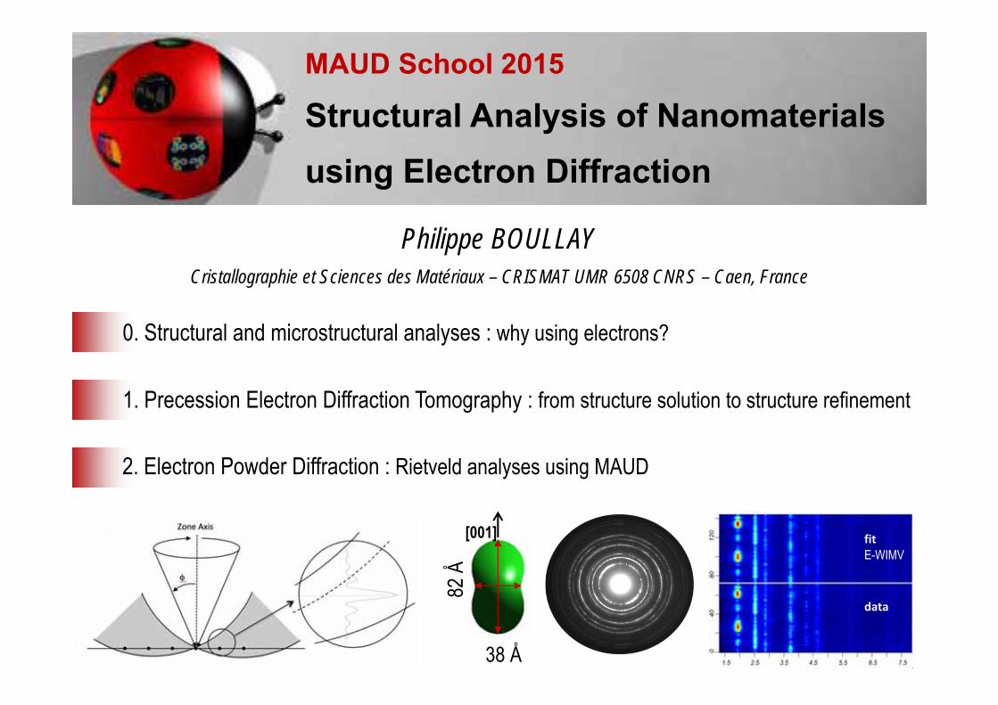
1. Precession Electron Diffraction Tomography : from structure solution to structure refinement
2. Electron Powder Diffraction : Rietveld analyses using MAUD
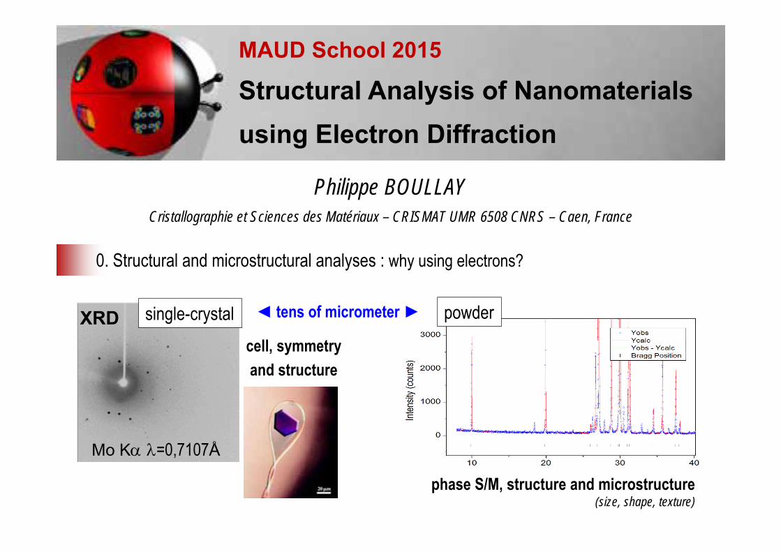
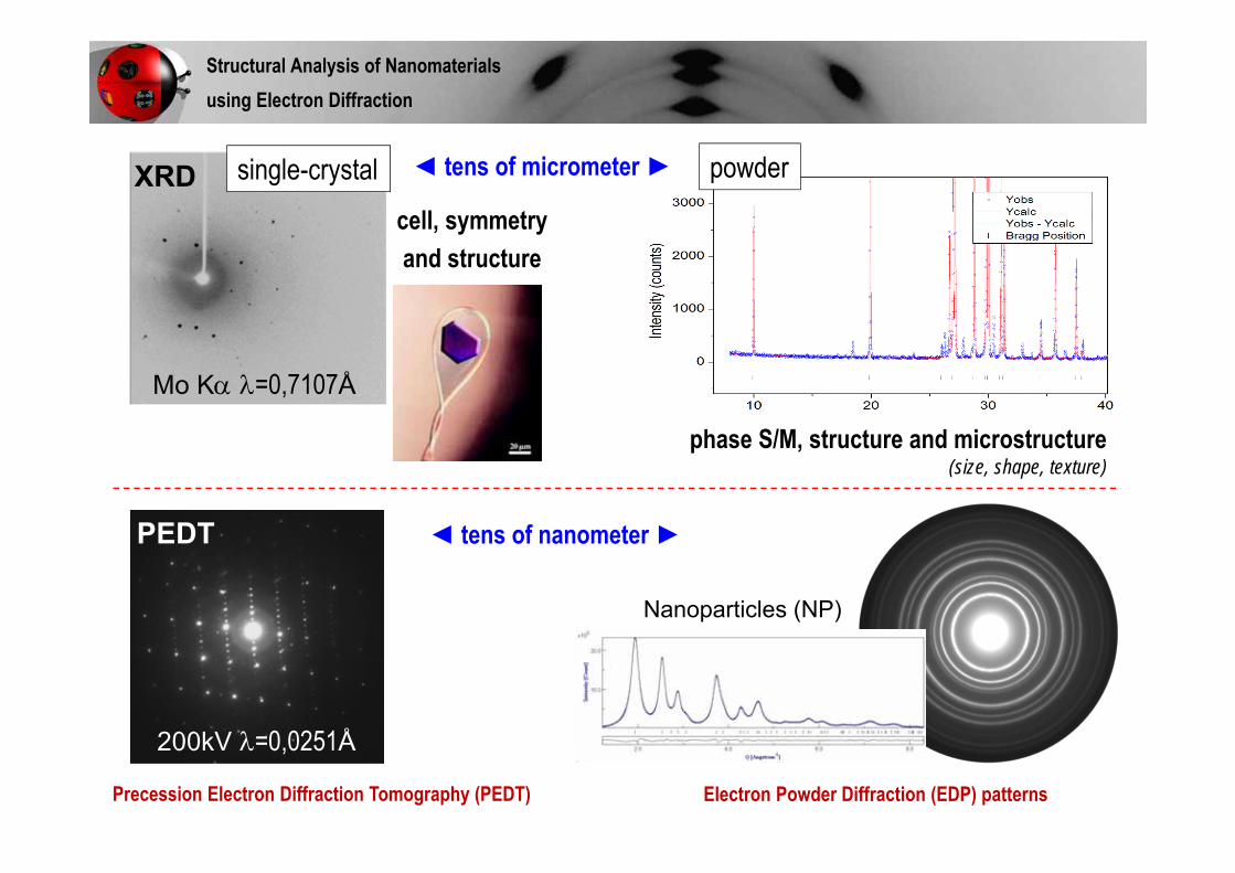
0. Structural and microstructural analyses : why using electrons?
82 Å
38 Å
[001]
data
fitE-WIMV
MAUD School 2015
Structural Analysis of Nanomaterialsusing Electron Diffraction
Philippe BOULLAYCristallographie et Sciences des Matériaux – CRISMAT UMR 6508 CNRS – Caen, France
phase S/M, structure and microstructure(size, shape, texture)
powder
cell, symmetry and structure
XRD
Mo K =0,7107Å
single-crystal ◄ tens of micrometer ►
0. Structural and microstructural analyses : why using electrons?
phase S/M, structure and microstructure(size, shape, texture)
powder
cell, symmetry and structure
XRD
Mo K =0,7107Å
single-crystal ◄ tens of micrometer ►
PEDT
200kV =0,0251Å
Precession Electron Diffraction Tomography (PEDT) Electron Powder Diffraction (EDP) patterns
Nanoparticles (NP)
Structural Analysis of Nanomaterialsusing Electron Diffraction
◄ tens of nanometer ►

Structural Analysis of Nanomaterialsusing Electron Diffraction
Amplitude scattered by a crystalline lattice
in “ 3D ”
atomic form factors
atomic positions
transmission function
atoms in the elementary unit cell crystal form factor
measure Ig=||Ag||2
the phase is lost
TF
Motif de diffractionFraunhofer Diffraction = FT of the transmission function of the object
TF‐1
structure factor
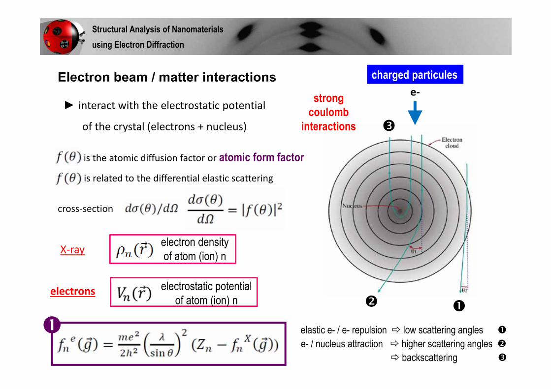
► interact with the electrostatic potential
of the crystal (electrons + nucleus)
Electron beam / matter interactions
Structural Analysis of Nanomaterialsusing Electron Diffraction
elastic e- / e- repulsion low scattering angles e- / nucleus attraction higher scattering angles
backscattering
e‐
strongcoulomb
interactions
is related to the differential elastic scattering
cross‐section :
electrons electrostatic potentialof atom (ion) n
X‐ray electron densityof atom (ion) n
is the atomic diffusion factor or atomic form factor
charged particules
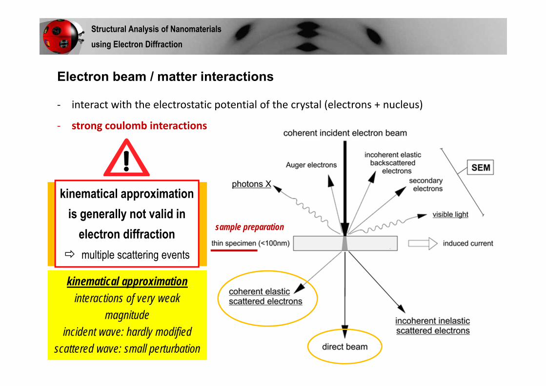
kinematical approximationinteractions of very weak
magnitudeincident wave: hardly modified
scattered wave: small perturbation
‐ interact with the electrostatic potential of the crystal (electrons + nucleus)
‐ strong coulomb interactions
Electron beam / matter interactions
diffractioncoherent elastic scattering
no energy or wavelength changeof the incident wave
Structural Analysis of Nanomaterialsusing Electron Diffraction
kinematical approximation is generally not valid in
electron diffraction multiple scattering events
sample preparation
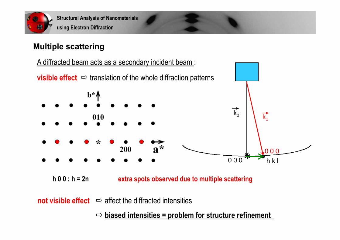
k0 k1
* 0 0 0 h k l 0 0 0
A diffracted beam acts as a secondary incident beam :
visible effect translation of the whole diffraction patterns
Multiple scattering
not visible effect affect the diffracted intensities
biased intensities = problem for structure refinement
Structural Analysis of Nanomaterialsusing Electron Diffraction
h 0 0 : h = 2n extra spots observed due to multiple scattering
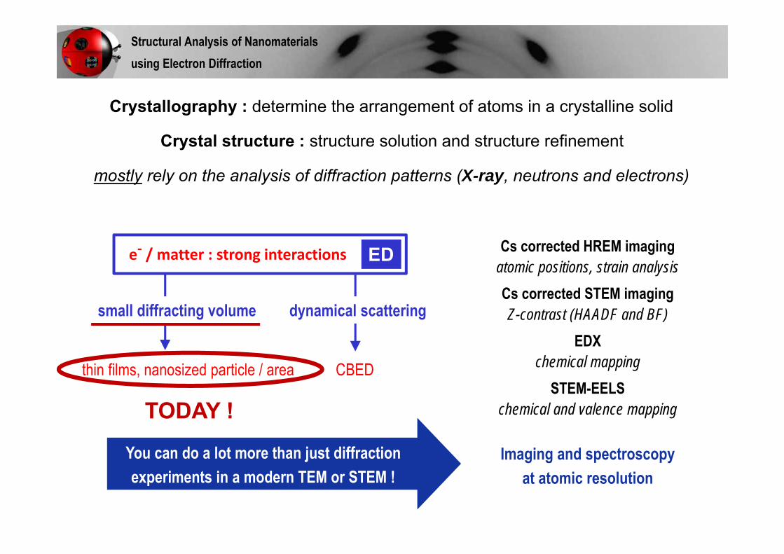
Crystallography : determine the arrangement of atoms in a crystalline solid
Crystal structure : structure solution and structure refinement
mostly rely on the analysis of diffraction patterns (X-ray, neutrons and electrons)
Cs corrected HREM imagingatomic positions, strain analysisCs corrected STEM imagingZ-contrast (HAADF and BF)
EDXchemical mapping
STEM-EELSchemical and valence mapping
You can do a lot more than just diffractionexperiments in a modern TEM or STEM !
Imaging and spectroscopyat atomic resolution
e‐ / matter : strong interactions
thin films, nanosized particle / area
ED
small diffracting volume
CBED
dynamical scattering
Structural Analysis of Nanomaterialsusing Electron Diffraction
TODAY !

10
O
IG
000
a*
b*
incident parallel e‐beam
Structural Analysis of Nanomaterialsusing Electron Diffraction
2dsin=nBragg’s law
11
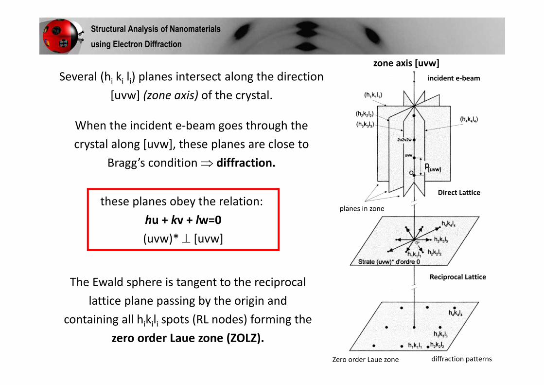
The Ewald sphere is tangent to the reciprocal lattice plane passing by the origin and
containing all hikili spots (RL nodes) forming the zero order Laue zone (ZOLZ).
these planes obey the relation: hu + kv + lw=0(uvw)* [uvw]
zone axis [uvw]
Direct Lattice
Several (hi ki li) planes intersect along the direction [uvw] (zone axis) of the crystal.
When the incident e‐beam goes through the crystal along [uvw], these planes are close to
Bragg’s condition diffraction.
incident e‐beam
Reciprocal Lattice
diffraction patternsZero order Laue zone
planes in zone
Structural Analysis of Nanomaterialsusing Electron Diffraction
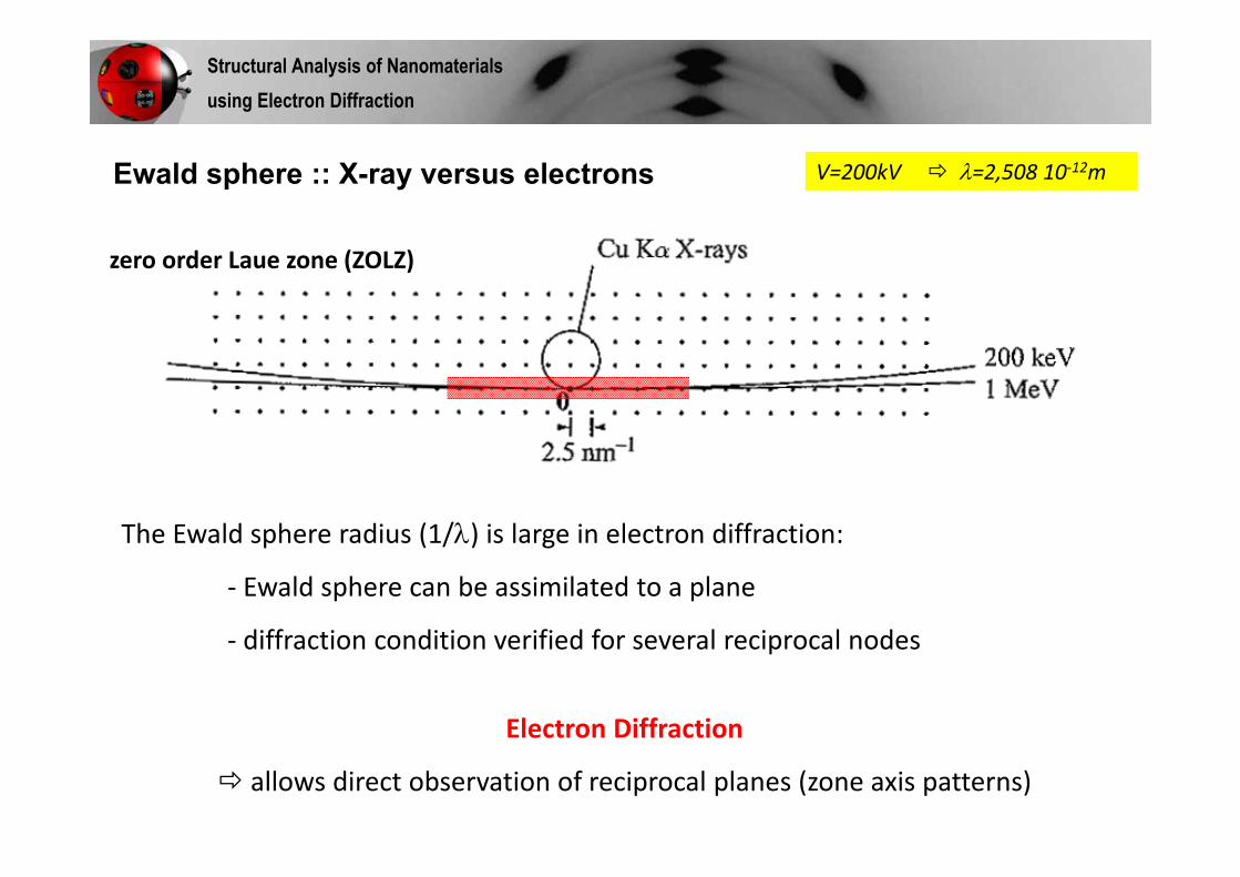
The Ewald sphere radius (1/) is large in electron diffraction:
‐ Ewald sphere can be assimilated to a plane
‐ diffraction condition verified for several reciprocal nodes
Electron Diffraction
allows direct observation of reciprocal planes (zone axis patterns)
Ewald sphere :: X-ray versus electrons
Structural Analysis of Nanomaterialsusing Electron Diffraction
zero order Laue zone (ZOLZ)
V=200kV =2,508 10‐12m
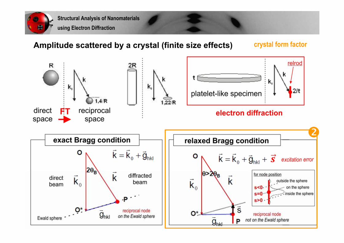
Amplitude scattered by a crystal (finite size effects) crystal form factor
Structural Analysis of Nanomaterialsusing Electron Diffraction
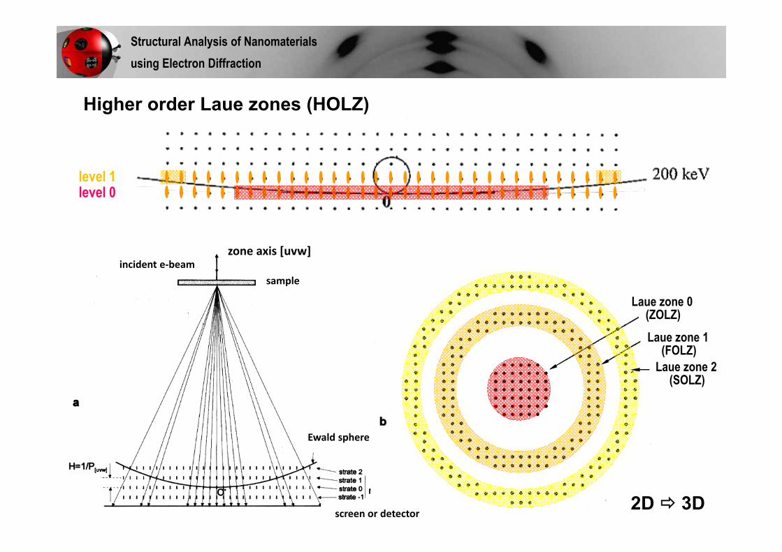
Higher order Laue zones (HOLZ)
level 0level 1
2D 3D
incident e‐beamzone axis [uvw]
sample
screen or detector
Ewald sphere
Laue zone 2(SOLZ)
Laue zone 0(ZOLZ)Laue zone 1
(FOLZ)
Structural Analysis of Nanomaterialsusing Electron Diffraction
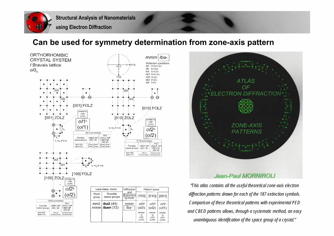
Can be used for symmetry determination from zone-axis pattern
“This atlas contains all the useful theoretical zone-axis electron
diffraction patterns drawn for each of the 187 extinction symbols.
Comparison of these theoretical patterns with experimental PED
and CBED patterns allows, through a systematic method, an easy
unambiguous identification of the space group of a crystal.”
Structural Analysis of Nanomaterialsusing Electron Diffraction

MAUD School 2015
Structural Analysis of Nanomaterialsusing Electron Diffraction
Philippe BOULLAYCristallographie et Sciences des Matériaux – CRISMAT UMR 6508 CNRS – Caen, France
1. Precession Electron Diffraction Tomography : from structure solution to structure refinement
a. Electron Diffraction Tomography (EDT)
b. Precession Electron Diffraction Tomography (PEDT)
c. PEDT and structure solution (kinematical approximation)
d. PEDT and structure refinement (dynamical approach)
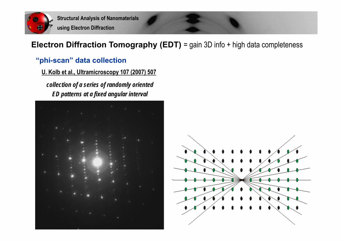
“phi-scan” data collectionU. Kolb et al., Ultramicroscopy 107 (2007) 507
collection of a series of randomly oriented ED patterns at a fixed angular interval
Structural Analysis of Nanomaterialsusing Electron Diffraction
Electron Diffraction Tomography (EDT) = gain 3D info + high data completeness
Structural Analysis of Nanomaterialsusing Electron Diffraction
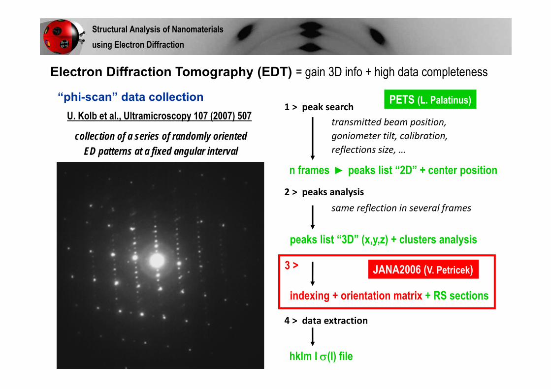
“phi-scan” data collection PETS (L. Palatinus)1 > peak search
transmitted beam position, goniometer tilt, calibration, reflections size, …
n frames ► peaks list “2D” + center position
2 > peaks analysissame reflection in several frames
peaks list “3D” (x,y,z) + clusters analysis
4 > data extraction
hklm I (I) file
indexing + orientation matrix + RS sections
JANA2006 (V. Petricek)3 >
U. Kolb et al., Ultramicroscopy 107 (2007) 507
collection of a series of randomly oriented ED patterns at a fixed angular interval
Electron Diffraction Tomography (EDT) = gain 3D info + high data completeness

- limit the interactions between the diffracted beams
- less sensitive to thickness variation
- increase the resolution limit
- integrated intensities
R. Vincent and P.A. Midgley, Ultramicroscopy 53 (1994) 271
► Electron crystallography : more complicated than XRD due to dynamical conditions
limit the dynamical effects
thin samples, light atoms, oblique texture ED, …
PED
4 > data extraction
hklm I (I) file
► EDT datasets : go further and use intensities for structure solution ?
structure ?
Structural Analysis of Nanomaterialsusing Electron Diffraction
Electron Diffraction Tomography (EDT) = gain 3D info + high data completeness
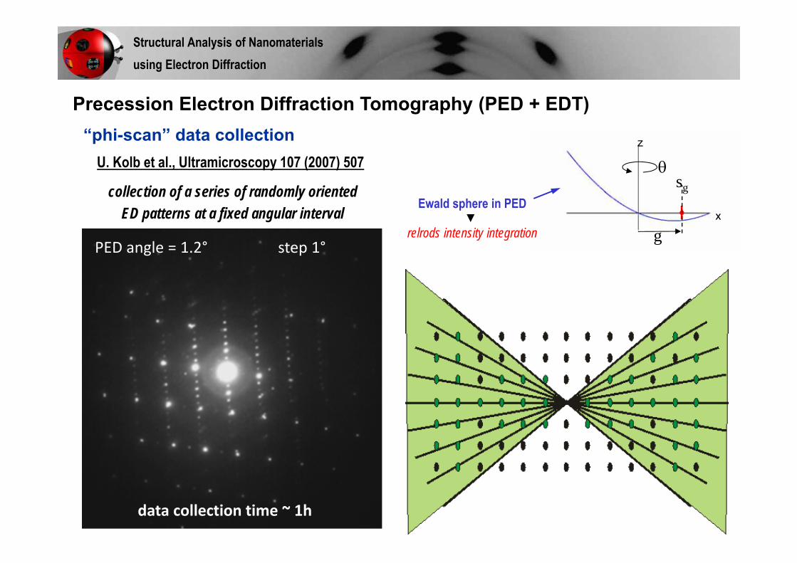
“phi-scan” data collectionU. Kolb et al., Ultramicroscopy 107 (2007) 507
collection of a series of randomly oriented ED patterns at a fixed angular interval x
z
sg
g
Ewald sphere in PED▼
relrods intensity integrationPED angle = 1.2° step 1°
data collection time ~ 1h
Precession Electron Diffraction Tomography (PED + EDT)
Structural Analysis of Nanomaterialsusing Electron Diffraction

Structural Analysis of Nanomaterialsusing Electron Diffraction
z
sg
g
Ewald sphere in PED
limit the dynamical effects PED
- limit the interactions between the diffracted beams- less sensitive to thickness variation- increase the resolution limit - integrated intensities
Data Analysis ►1 hkl I (I) file
NdGaO3 Pnma ap√2 x 2ap x ap√2
~1,75°
~0,8°
increase the data completeness EDT
Precession Electron Diffraction Tomography
structure solutionkinematical approximation
structure refinement
PEDT
zone‐axis PED
Precession Electron Diffraction Tomography (PED + EDT)
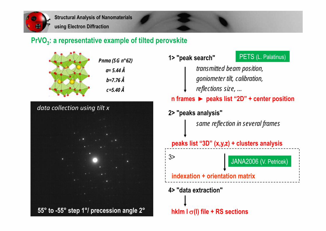
55° to -55° step 1°/ precession angle 2°
data collection using tilt x
PETS (L. Palatinus)1> "peak search"transmitted beam position, goniometer tilt, calibration, reflections size, …
n frames ► peaks list “2D” + center position
2> "peaks analysis"same reflection in several frames
peaks list “3D” (x,y,z) + clusters analysis
4> "data extraction"
hklm I (I) file + RS sections
indexation + orientation matrix
JANA2006 (V. Petricek)3>
PrVO3: a representative example of tilted perovskite
Structural Analysis of Nanomaterialsusing Electron Diffraction
Pnma (SG n°62)
a= 5.44 Å
b=7.76 Å
c=5.40 Å

Data Analysis > like single crystal XRD Phi scan
-55° to +55°, step 1°
PED angle: 2.0°
111 unoriented patterns nb. Of reflections : ~ 1050 [I> 3σ(I)]_Acquisition time ≈ 20 min
a*
c*
Lattice indexationa ≈ 5,471 Å; b ≈ 7,698 Å; c ≈ 5,356 Å;
α ≈ β≈ γ ≈ 90°Parameters:
*.xyz
coverage 1Å shell ~98%
Structural Analysis of Nanomaterialsusing Electron Diffraction

Check symmetry using reciprocal space sections
(0kl) (1kl) (h0l)
Orthorhombic Pnmaa = 5,47 Å; b = 7,69 Å; c = 5,36 Å
(hk0) (hk1) ►
►
►
c* c*
b* b*
c*
a*
a*a*
b* b*
PETS
Structural Analysis of Nanomaterialsusing Electron Diffraction
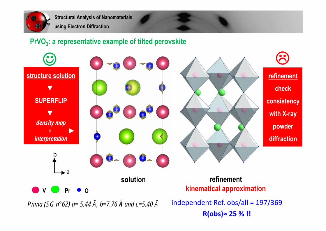
Electron density map
Pnma (SG n°62) a= 5.44 Å, b=7.76 Å and c=5.40 Å
b
asolution refinement
kinematical approximation V Pr O
independent Ref. obs/all = 197/369R(obs)≈ 25 % !!
PrVO3: a representative example of tilted perovskite
Structural Analysis of Nanomaterialsusing Electron Diffraction
structure solution
▼
SUPERFLIP
▼density map
+ ►interpretation
refinement
check
consistency
with X-ray
powder
diffraction

► does it means that this structure is wrong ?
Residual dynamic effects !
reliability factors calculated based onkinematical approximation are biased
Pnma (SG n°62) a= 5.44 Å, b=7.76 Å and c=5.40 Å
* M.J. Martinez-Lope et al., Inorg. Chem. 47 (2008) 2634-2640
ADRA= Average Distance of Reference Atoms(comparison with the
NPD reference*)
confidence ?
Kinematicaldist. restric.
PrVO3
PrVO3: a representative example of tilted perovskite
Structural Analysis of Nanomaterialsusing Electron Diffraction
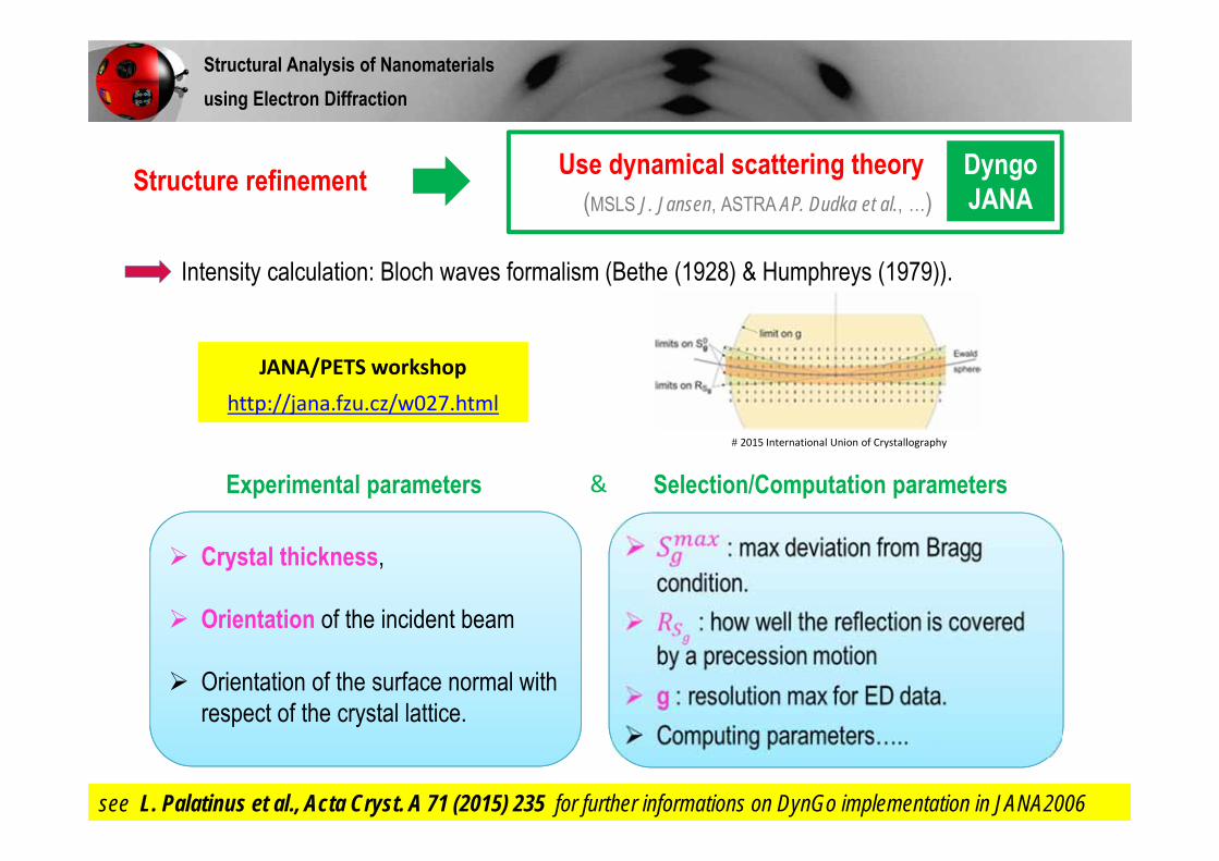
Use dynamical scattering theory DyngoJANAStructure refinement
(MSLS J. Jansen, ASTRA AP. Dudka et al., …)
see L. Palatinus et al., Acta Cryst. A 71 (2015) 235 for further informations on DynGo implementation in JANA2006
Intensity calculation: Bloch waves formalism (Bethe (1928) & Humphreys (1979)).
Experimental parameters Selection/Computation parameters&
Crystal thickness,
Orientation of the incident beam
Orientation of the surface normal withrespect of the crystal lattice.
# 2015 International Union of Crystallography
JANA/PETS workshophttp://jana.fzu.cz/w027.html
Structural Analysis of Nanomaterialsusing Electron Diffraction

d* limit
► Dedicated integration procedure of intensities for each frame : list of reflections, hkl , intensity, scale and estimated standard deviation σ(I)
PETS
► Parameters optimization JANA2006
thickness
R-factor
Thickness optimization
~280 nm
orientation optimization
►n hkl I (I) files !
Structural Analysis of Nanomaterialsusing Electron Diffraction

► Dynamical refinement results (no distance constraints and no data selection: 111 PED patterns)
Towards accurate structure refinement with an accuracycomparable to XRD and NPD
better▼
accuracy
confidence
L. Palatinus et al., submitted Structure refinement using precession electron diffraction tomography and dynamical diffraction
►111 frames
Dynamicalref. + ADP
Dynamical ref. + aniso. ADP PrVO3
dynamical refinement
Structural Analysis of Nanomaterialsusing Electron Diffraction
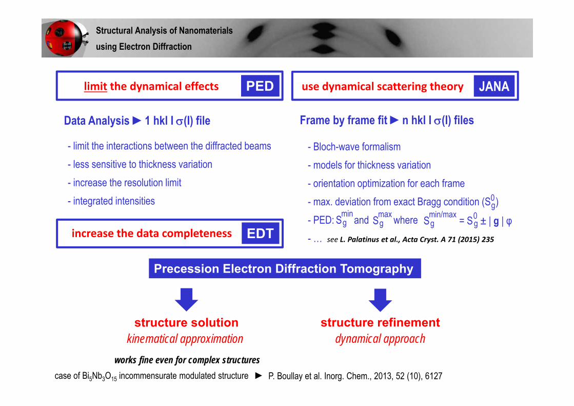
limit the dynamical effects PED
- limit the interactions between the diffracted beams- less sensitive to thickness variation- increase the resolution limit - integrated intensities
Data Analysis ►1 hkl I (I) file
structure solutionkinematical approximation
increase the data completeness EDT
Precession Electron Diffraction Tomography
works fine even for complex structurescase of Bi5Nb3O15 incommensurate modulated structure ►
use dynamical scattering theory JANA
Frame by frame fit ►n hkl I (I) files
- Bloch-wave formalism- models for thickness variation- orientation optimization for each frame- max. deviation from exact Bragg condition (S )- PED: and where- …
g0
Sgmin
Sgmax S = S ± | g | φg
min/maxg0
see L. Palatinus et al., Acta Cryst. A 71 (2015) 235
structure refinementdynamical approach
P. Boullay et al. Inorg. Chem., 2013, 52 (10), 6127
Structural Analysis of Nanomaterialsusing Electron Diffraction

Structural Analysis of Nanomaterialsusing Electron Diffraction
More crystals more reflections, resulting in concentric rings with a central beam in the middle
◄ tens of nanometer ►PEDT
single crystal Electron Powder Diffraction (EDP) patterns
Nanoparticles (NP)
1 2x 4x
…
single crystal
MAUD School 2015
Structural Analysis of Nanomaterialsusing Electron Diffraction
Philippe BOULLAYCristallographie et Sciences des Matériaux – CRISMAT UMR 6508 CNRS – Caen, France
2. Electron Powder Diffraction : Rietveld analyses using MAUD
a. phase search and indexing
b. sizes, shapes and textures
c. structure refinements
P. Boullay, L. Lutterotti, D. chateigner and L. Sicard, Acta Cryst. A 70 (2014) 448-456 Fast Microstructure and Phase Analyses of Nanopowders using Combined Analysis of TEM scattering patterns

Quantitative and statistically representative analysis of crystallite
sizes and shapes, structure and crystallographic texture of
nanoparticles in the form of powders and thin films?
Extraction of intensities from electron diffraction “ring patterns” for quantitative or semi-quantitative analysis …
Vainshtein (1964), …
PCED 2.0 : X.Z. Li, Ultramicroscopy 110 (2010) 297-304
ProcessDiffraction : J.L. Labar, Microsc. Microanal. 15 (2009) 20-29
TextPat : P. Oleynikov, S. Hovmoller and X.D. Zou in Electron Crystallography
The MAUD program : L. Lutterotti Nuclear Inst. and Methods in Physics Res. B268 (2010) 334-340.
Structural Analysis of Nanomaterialsusing Electron Diffraction
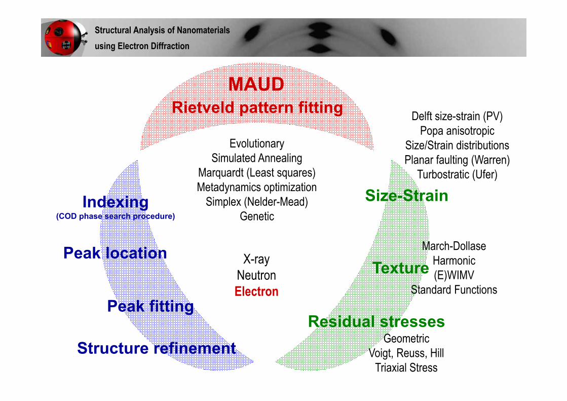
Size-Strain
Texture
Residual stresses
March-DollaseHarmonic(E)WIMV
Standard Functions
GeometricVoigt, Reuss, Hill
Triaxial Stress
Delft size-strain (PV)Popa anisotropic
Size/Strain distributionsPlanar faulting (Warren)
Turbostratic (Ufer)
EvolutionarySimulated Annealing
Marquardt (Least squares)Metadynamics optimization
Simplex (Nelder-Mead)Genetic
X-rayNeutronElectron
Rietveld pattern fittingMAUD
Indexing(COD phase search procedure)
Peak location
Peak fitting
Structure refinement
Structural Analysis of Nanomaterialsusing Electron Diffraction
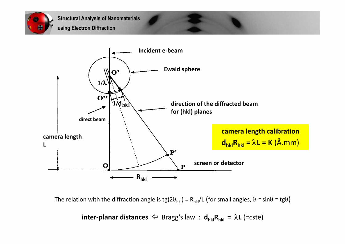
The relation with the diffraction angle is tg(2hkl) = Rhkl/L (for small angles, ~ sin ~ tg)
inter‐planar distances Bragg’s law : dhklRhkl = L (=cste)
Rhkl
camera length calibrationdhklRhkl = L = K (Å.mm)
camera length L
Incident e‐beam
direct beam
Ewald sphere
direction of the diffracted beam for (hkl) planes
screen or detector
Structural Analysis of Nanomaterialsusing Electron Diffraction

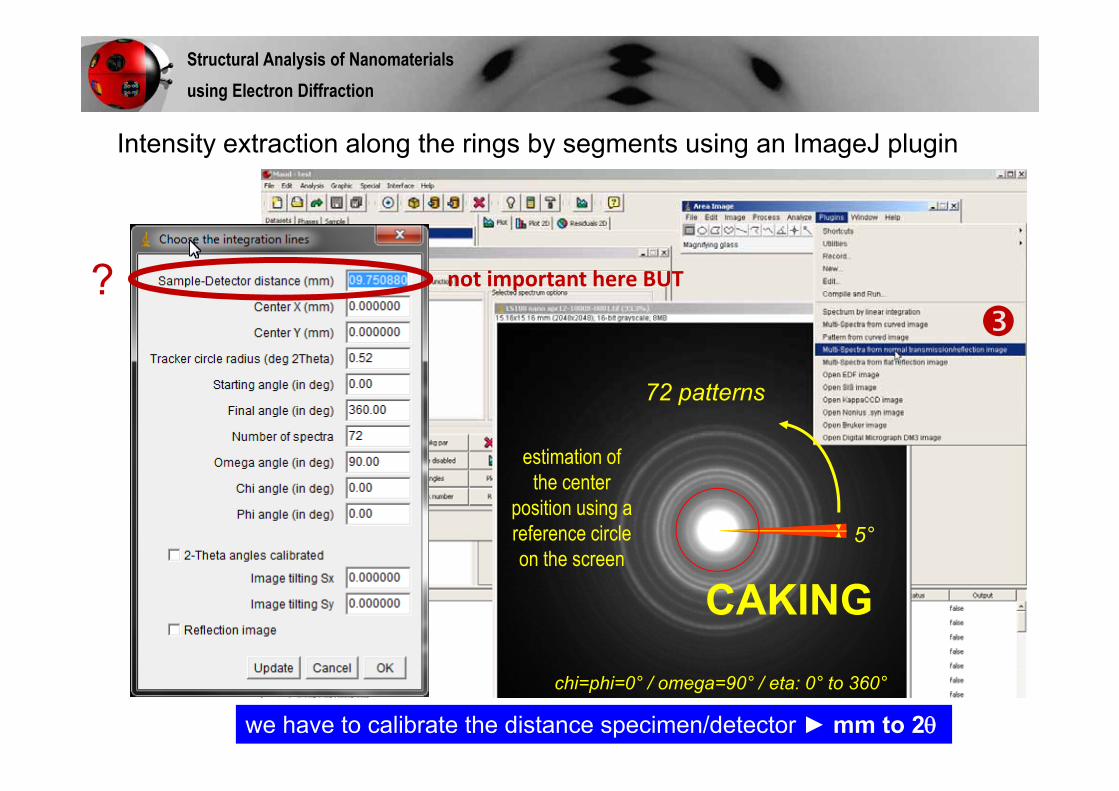
Intensity extraction along the rings by segments using an ImageJ plugin
Structural Analysis of Nanomaterialsusing Electron Diffraction
only dependent of the specification of your CCD camera► pixel to mm
pixel size

Intensity extraction along the rings by segments using an ImageJ plugin
Structural Analysis of Nanomaterialsusing Electron Diffraction
Transmission geometry for TEM scattering experiments with the nomenclature used in MAUD
3°
120 patterns
CAKING
chi=phi=0° / omega=90° / eta: 0° to 360°

Intensity extraction along the rings by segments using an ImageJ plugin
5°
72 patterns
CAKING
chi=phi=0° / omega=90° / eta: 0° to 360°
estimation of the center
position using a reference circle on the screen
Structural Analysis of Nanomaterialsusing Electron Diffraction

Pawley fitting without refining center or tiltingCentre defined graphically on the image Rwp = 2.83 %
Pawley fitting refining center but not tilting x-center error = -0.00717(5) mmy-center error = -0.01278(5) mmRwp = 2.32 %
Corrections for center position and elliptical distortion ?
Pawley fitting refining centre and tiltingx-center error = -0.00755(4) mmy-center error = -0.01093(4) mmtilting error x (sin(error)) = -0.0048(3)tilting error y (sin(error)) = 0.1211(3)Rwp = 1.56 %
Structural Analysis of Nanomaterialsusing Electron Diffraction
Intensity extraction along the rings by segments using an ImageJ plugin
5°
72 patterns
CAKING
chi=phi=0° / omega=90° / eta: 0° to 360°
estimation of the center
position using a reference circle on the screen
Structural Analysis of Nanomaterialsusing Electron Diffraction
we have to calibrate the distance specimen/detector ► mm to 2
? not important here BUT
Intensity extraction along the rings by segments using an ImageJ plugin
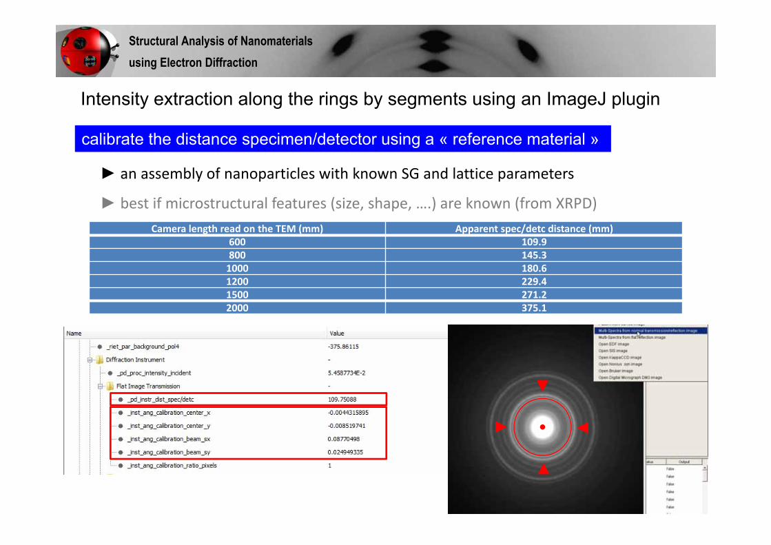
Structural Analysis of Nanomaterialsusing Electron Diffraction
calibrate the distance specimen/detector using a « reference material »
▼
▼▼
▼
► an assembly of nanoparticles with known SG and lattice parameters
► best if microstructural features (size, shape, ….) are known (from XRPD) Camera length read on the TEM (mm) Apparent spec/detc distance (mm)
600 109.9800 145.31000 180.61200 229.41500 271.22000 375.1

Intensity extraction along the rings by segments using an ImageJ plugin
3°
120 patterns
CAKING
chi=phi=0° / omega=90° / eta: 0° to 360°
estimation of the center
position using a reference circle on the screen
2D plot
Structural Analysis of Nanomaterialsusing Electron Diffraction

2 (°) => Q (Å-1)
b(x): background => pic at 0° + polynomial function
peak location and intensities
1D XRPD-like pattern (360° summed intensity)
measured profile h(x) = f(x) g(x) + b(x)
Structural Analysis of Nanomaterialsusing Electron Diffraction
Database Pattern
Rietveld fit(for each phase inthe database)
RankingAdd newphases
Best phase> threshold N End:
RietveldY
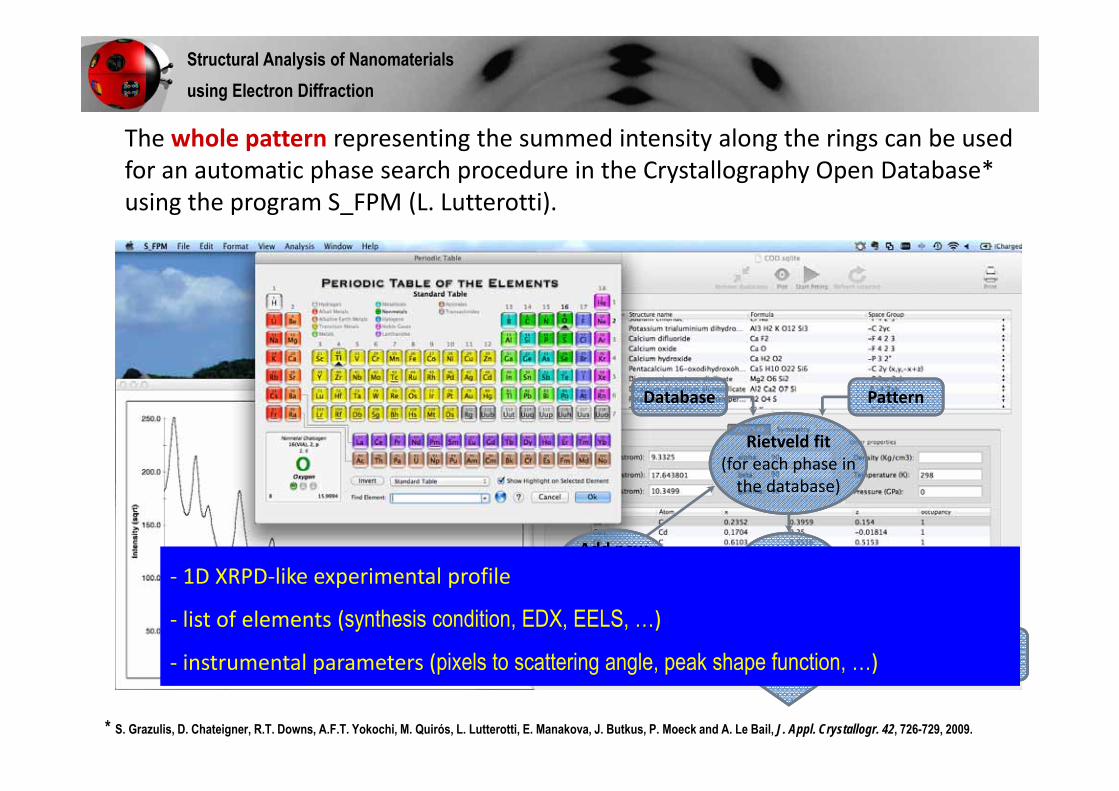
The whole pattern representing the summed intensity along the rings can be used for an automatic phase search procedure in the Crystallography Open Database* using the program S_FPM (L. Lutterotti).
* S. Grazulis, D. Chateigner, R.T. Downs, A.F.T. Yokochi, M. Quirós, L. Lutterotti, E. Manakova, J. Butkus, P. Moeck and A. Le Bail, J. Appl. Crystallogr. 42, 726-729, 2009.
‐ 1D XRPD‐like experimental profile
‐ list of elements (synthesis condition, EDX, EELS, …)
‐ instrumental parameters (pixels to scattering angle, peak shape function, …)
Structural Analysis of Nanomaterialsusing Electron Diffraction
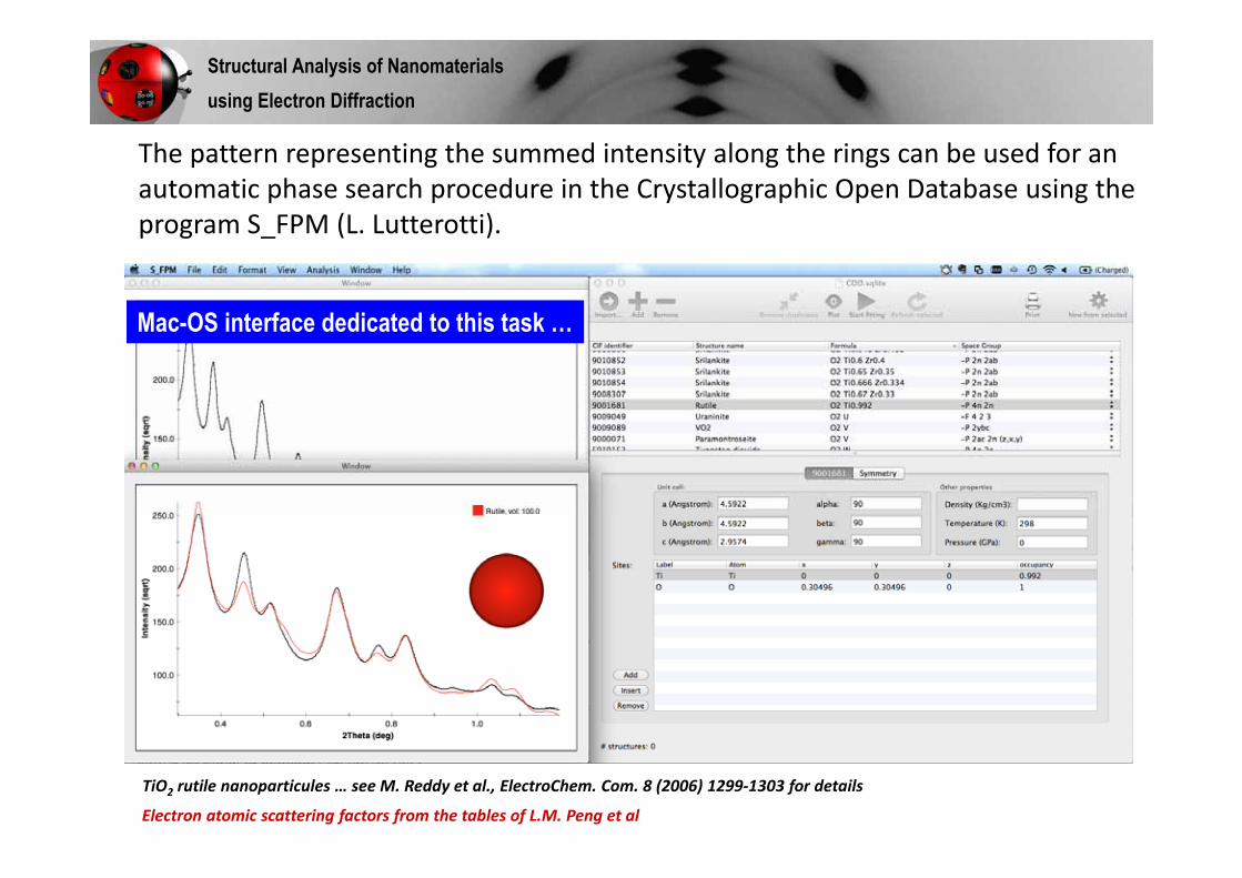
TiO2 rutile nanoparticules … see M. Reddy et al., ElectroChem. Com. 8 (2006) 1299‐1303 for details
The pattern representing the summed intensity along the rings can be used for an automatic phase search procedure in the Crystallographic Open Database using the program S_FPM (L. Lutterotti).
Electron atomic scattering factors from the tables of L.M. Peng et al
Structural Analysis of Nanomaterialsusing Electron Diffraction
Mac-OS interface dedicated to this task …

kinematicapproximation is used tocalculate the whole pattern profile
http://nanoair.dii.unitn.it:8080/sfpm and http://cod.iutcaen.unicaen.fr
automatic phase search procedure is possible (COD database, multi-phases)
Structural Analysis of Nanomaterialsusing Electron Diffraction
a web site dedicated to this task is available
Test on nanopowders (TiO2 rutile, Mn3O4 hausmannite, CoFe2O4 spinel) and textured
thin films (MgO on Pt)
• low texture : one single ED‐RP is sufficient
• strong texture : more tricky …need more than one ED‐RP
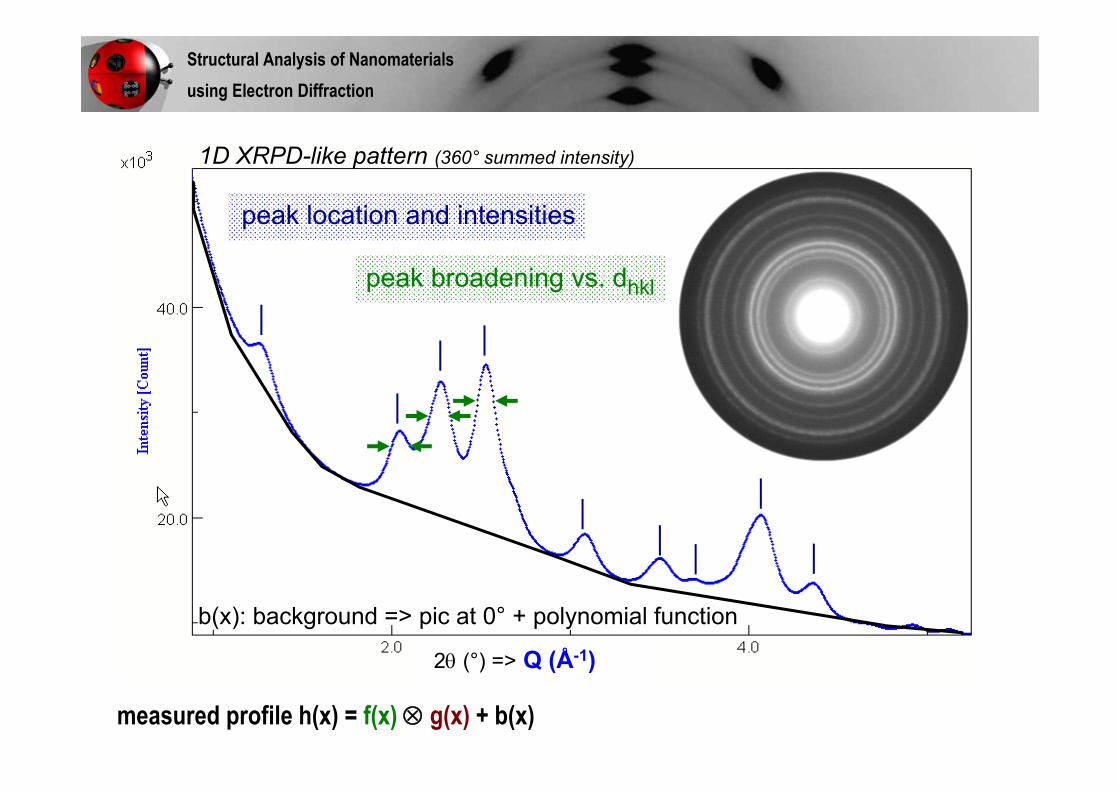
2 (°) => Q (Å-1)
b(x): background => pic at 0° + polynomial function
peak location and intensities
peak broadening vs. dhkl
1D XRPD-like pattern (360° summed intensity)
measured profile h(x) = f(x) g(x) + b(x)
Structural Analysis of Nanomaterialsusing Electron Diffraction
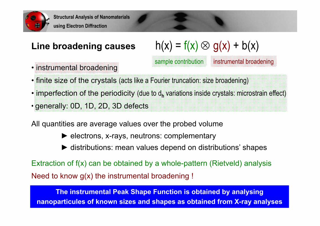
h(x) = f(x) g(x) + b(x)sample contribution instrumental broadening
Extraction of f(x) can be obtained by a whole-pattern (Rietveld) analysis
Line broadening causes
• instrumental broadening
• finite size of the crystals (acts like a Fourier truncation: size broadening)• imperfection of the periodicity (due to dh variations inside crystals: microstrain effect)• generally: 0D, 1D, 2D, 3D defects
All quantities are average values over the probed volume ► electrons, x-rays, neutrons: complementary► distributions: mean values depend on distributions’ shapes
Need to know g(x) the instrumental broadening !
L. Lutterotti and P. Scardi, J. of Appl. Crystallogr. 23, 246-252 (1990)The instrumental Peak Shape Function is obtained by analysing nanoparticules of known sizes and shapes as obtained from X-ray analyses
Structural Analysis of Nanomaterialsusing Electron Diffraction
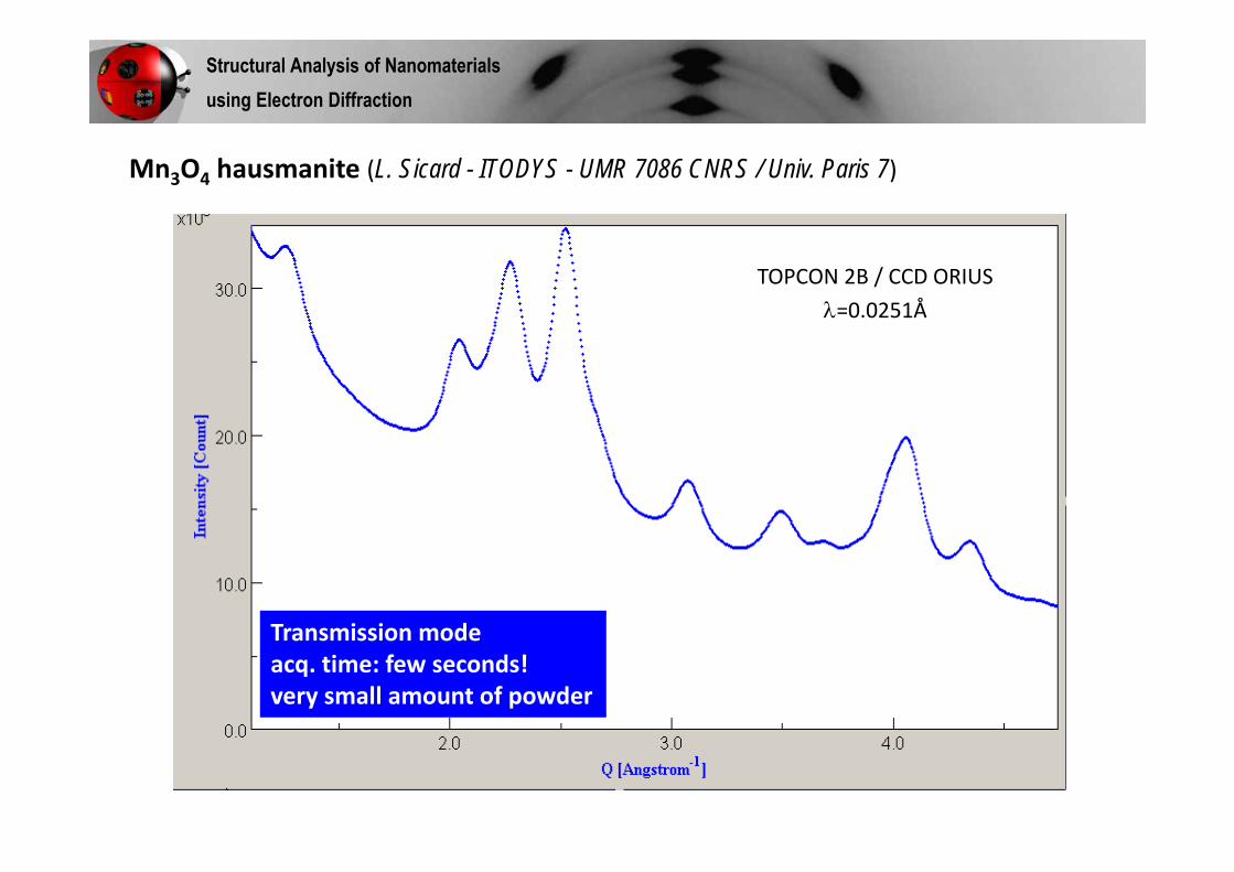
Reflection modeacq. time:3h30 > 100mg powder
Transmission modeacq. time:6hpowder in a capillary
Mn3O4 hausmanite (L. Sicard - ITODYS - UMR 7086 CNRS / Univ. Paris 7)
Structural Analysis of Nanomaterialsusing Electron Diffraction
Bruker D8 / Lynx Eye 1D =1.54056 Å (Cu K1)
SG: I 41/a m d a=5.764(2)Å and c=9.448(4)Å
Transmission modeacq. time: few seconds!very small amount of powder
TOPCON 2B / CCD ORIUS=0.0251Å
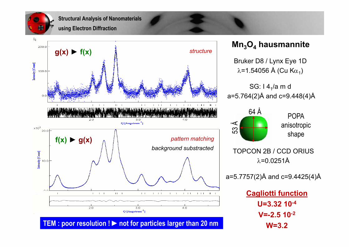
Mn3O4 hausmannite
Bruker D8 / Lynx Eye 1D =1.54056 Å (Cu K1)
SG: I 41/a m d a=5.764(2)Å and c=9.448(4)Å
TOPCON 2B / CCD ORIUS=0.0251Å
a=5.7757(2)Å and c=9.4425(4)Å
53 Å
64 Å
pattern matching
structure
POPAanisotropic
shape
g(x) ► f(x)
f(x) ► g(x)background substracted
Structural Analysis of Nanomaterialsusing Electron Diffraction
TEM : poor resolution ! ►not for particles larger than 20 nm
Cagliotti functionU=3.32 10-4
V=-2.5 10-2
W=3.2

TOPCON 2B / CCD ORIUS=0.0251Å
a=5.7757(2)Å and c=9.4425(4)Å
53 Å
64 Å POPAanisotropic
shape
f(x) ► g(x)
Structural Analysis of Nanomaterialsusing Electron Diffraction
Mn3O4 hausmannite
20nm
5°
72 patterns
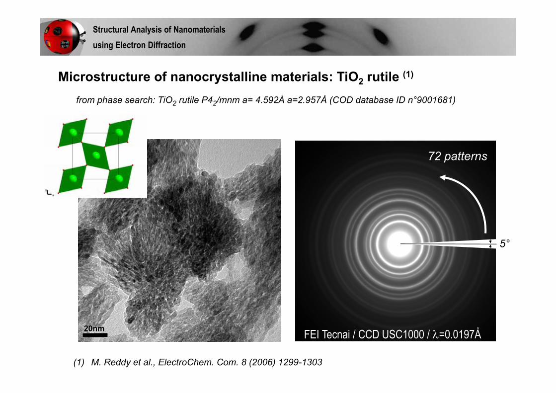
Microstructure of nanocrystalline materials: TiO2 rutile (1)
(1) M. Reddy et al., ElectroChem. Com. 8 (2006) 1299-1303
FEI Tecnai / CCD USC1000 / =0.0197Å
from phase search: TiO2 rutile P42/mnm a= 4.592Å a=2.957Å (COD database ID n°9001681)
Structural Analysis of Nanomaterialsusing Electron Diffraction
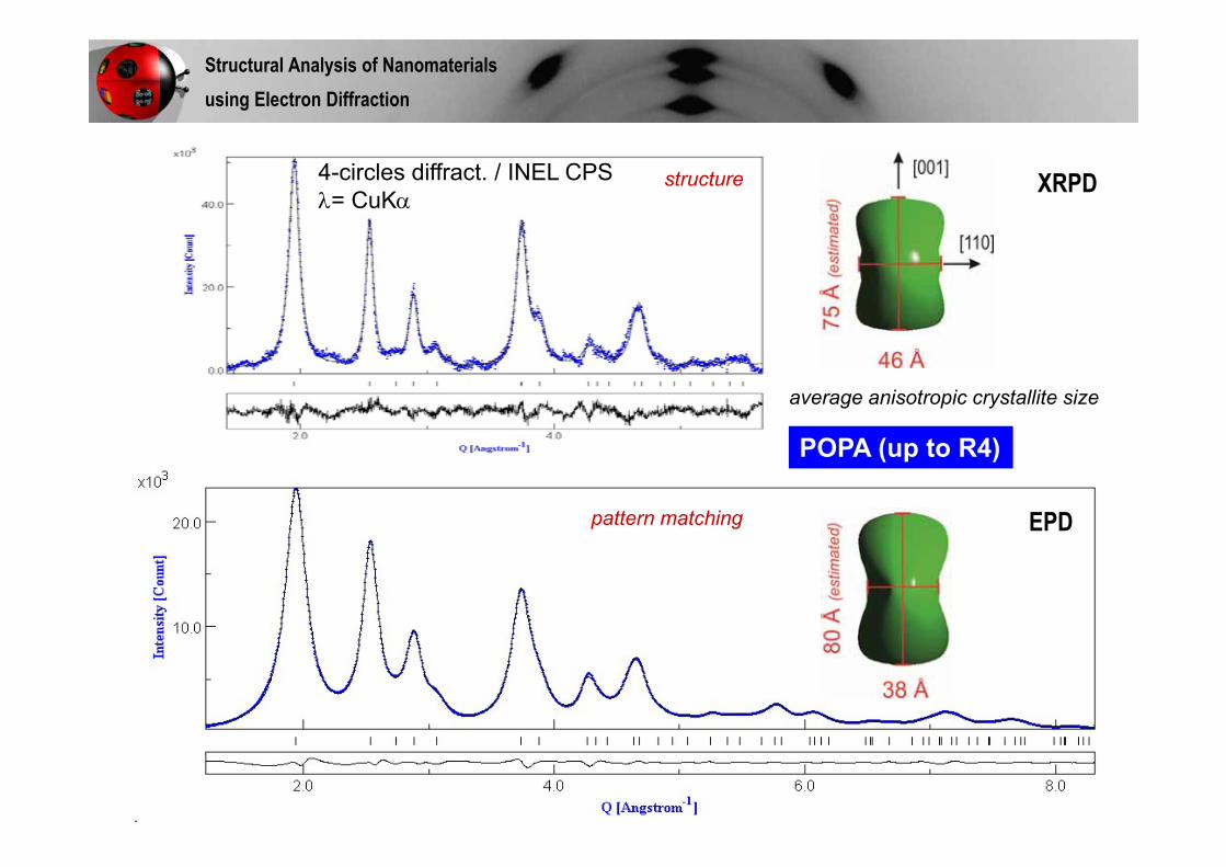
XRPD
EPD
average anisotropic crystallite size
structure
pattern matching
4-circles diffract. / INEL CPS= CuK
Structural Analysis of Nanomaterialsusing Electron Diffraction
POPA (up to R4)

Structural Analysis of Nanomaterialsusing Electron Diffraction
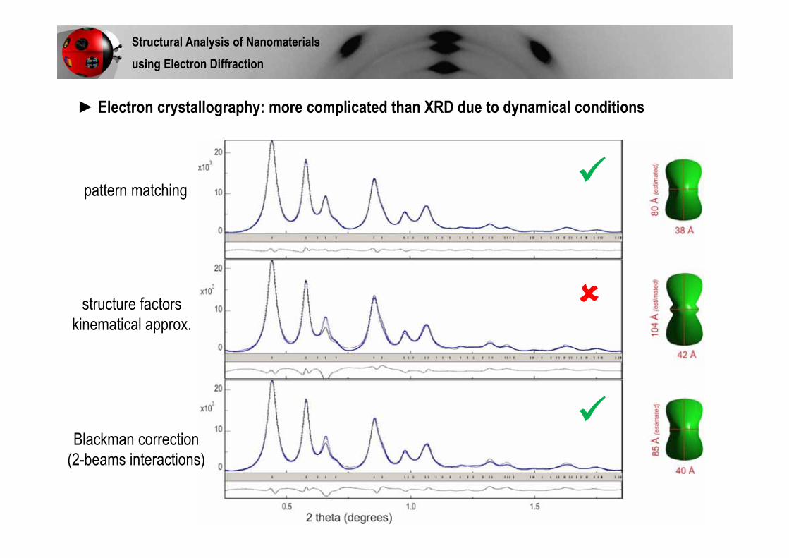
pattern matching
structure factorskinematical approx.
► microstructural features can be obtained in the pattern-matching mode
► not convincing using structure factors from kinematical approximation …
► Electron crystallography: more complicated than XRD due to dynamical conditions
Take into account dynamical conditions ?
Structural Analysis of Nanomaterialsusing Electron Diffraction
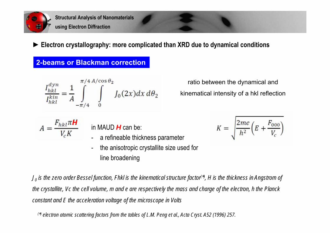
► Electron crystallography: more complicated than XRD due to dynamical conditions
2-beams or Blackman correction
ratio between the dynamical and
kinematical intensity of a hkl reflection
(*) electron atomic scattering factors from the tables of L.M. Peng et al., Acta Cryst. A52 (1996) 257.
J0 is the zero order Bessel function, Fhkl is the kinematical structure factor(*), H is the thickness in Angstrom of
the crystallite, Vc the cell volume, m and e are respectively the mass and charge of the electron, h the Planck
constant and E the acceleration voltage of the microscope in Volts
in MAUD H can be:- a refineable thickness parameter- the anisotropic crystallite size used for
line broadening
H
Structural Analysis of Nanomaterialsusing Electron Diffraction
pattern matching
structure factorskinematical approx.
Blackman correction(2-beams interactions)
► Electron crystallography: more complicated than XRD due to dynamical conditions
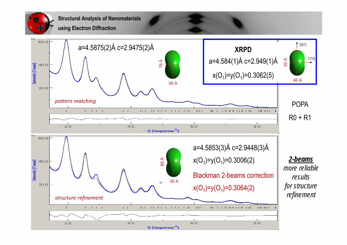
pattern matching
structure refinement
a=4.5853(3)Å c=2.9448(3)Åx(O1)=y(O1)=0.3006(2)
Blackman 2-beams correctionx(O1)=y(O1)=0.3064(2)
a=4.5875(2)Å c=2.9475(2)Å
Structural Analysis of Nanomaterialsusing Electron Diffraction
XRPDa=4.584(1)Å c=2.949(1)Å
x(O1)=y(O1)=0.3062(5)
POPA
R0 + R1
2-beamsmore reliable
resultsfor structure refinement

decreasing the selected area
0.5μm
data
fitno texture
Q (Å-1)
6μm
data
fitE-WIMV
Q (Å-1)
intensity variation along the rings
Structural Analysis of Nanomaterialsusing Electron Diffraction
local textureanalysis

QTA analysis of Pt thin film deposited on Si
The features available in MAUD allow a full quantitative texture analysis for general cases
(not only fiber textures) from EPD patterns with the obtention of accurate pole figures
(11 EPD patterns from +25° to -25° step 5°)
{111} pole figure from ODF refinement
Structural Analysis of Nanomaterialsusing Electron Diffraction
coverage
Tested using both Pawley structure factors extraction or Blackman structure factors calculationconsidering E-WIMV ODF refinement and one fiber texture component

NP TiO2 rutile
TEM =0.0251Å
synchrotron =0.486Å
I=f(Q)
CuK (150o 2)
√I*Q=f(Q)
see A.M.M. Abeykoon, C.D. Malliakas, P. Juhás, E.S. Božin, M.G. Kanatzidis, S.J.L. Billinge, Z. Kristallogr. 227 (2012) 248T.E. Gorelik, M.U. Schmidt; U. Kolb, S.J.L. Billinge, Microscopy and Microanalysis 21 (2015) 459
Structural Analysis of Nanomaterialsusing Electron Diffraction
PDF analyses on EPD ?
What can we do
in MAUD ?
▼
Rietveld “PDF-like”

Structural Analysis of Nanomaterialsusing Electron Diffraction
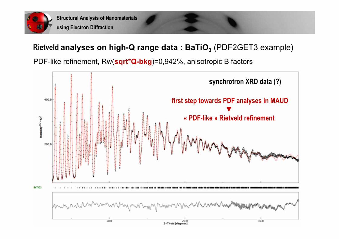
Rietveld analyses on high-Q range data : BaTiO3 (PDF2GET3 example)
normal refinement, sqrt statistic, anisotropic B factors : Rw=1.81%
synchrotron XRD data (?)
badly fitted▼
give more weight to high-Q
Structural Analysis of Nanomaterialsusing Electron Diffraction
Rietveld analyses on high-Q range data : BaTiO3 (PDF2GET3 example)
PDF-like refinement, Rw(sqrt*Q-bkg)=0,942%, anisotropic B factors
synchrotron XRD data (?)
first step towards PDF analyses in MAUD▼
« PDF-like » Rietveld refinement
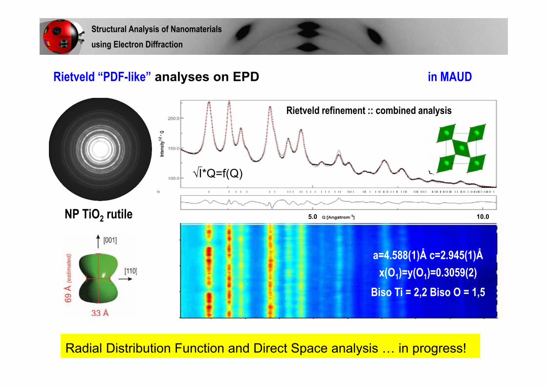
NP TiO2 rutile
√I*Q=f(Q)
5.0 10.0
a=4.588(1)Å c=2.945(1)Å x(O1)=y(O1)=0.3059(2)
Biso Ti = 2,2 Biso O = 1,5
Rietveld refinement :: combined analysis
Structural Analysis of Nanomaterialsusing Electron Diffraction
Rietveld “PDF-like” analyses on EPD in MAUD
Radial Distribution Function and Direct Space analysis … in progress!