structural and electrical properties of nickel zinc .... introduction ferrites are wide ... x-ray...
TRANSCRIPT

American Journal of Engineering Research (AJER) 2018
American Journal of Engineering Research (AJER)
e-ISSN: 2320-0847 p-ISSN : 2320-0936
Volume-7, Issue-3, pp-338-347
www.ajer.org Research Paper Open Access
w w w . a j e r . o r g
Page 338
Structural and Electrical Properties of Nickel Zinc Ferrite
Nanoparticles
Md. Thesun Al-Amin 1*
, Md. Feroz Alam Khan 2, Md. Ruhul Amin
1
1 Department of Electrical and Electronic Engineering (EEE)
Islamic University of Technology (IUT), Board Bazar, Gazipur-1704, Bangladesh. 2Department of Physics,
Bangladesh University of Engineering and Technology (BUET), Dhaka-1000, Bangladesh.
Corresponding author: Md. Thesun Al-Amin
ABSTRACT—Nickel Zinc Ferrite (NZF) nanoparticles were prepared by solid state reaction method. Nickel,
zinc and iron oxides were used as raw materials. The crystal structure characterization and morphology were
investigated by scanning electron microscopy (SEM) and X-ray diffraction (XRD) respectively. Annealing the
sample at high temperature provides better microstructure. Energy dispersive X-ray (EDX) was used to study
the elemental composition of the sample. The temperature dependent impedance of the sample was examined
using a high frequency impedance analyzer. This provides us an equivalent circuit which matches with the
simulated result. The percentage composition of the sample was found from X-ray fluorescence (XRF)
technique. Observing all characteristics of the sample we concluded that this sample would be better for the
application in the electronic devices near 30 MHz.
KEYWORDS— Ferrite, Nanoparticles, XRD, SEM, EDX, XRF, Impedance Analyzer.
----------------------------------------------------------------------------------------------------------------------------- ----------
Date of Submission: 17-03-2018 Date of acceptance: 01-04-2018
----------------------------------------------------------------------------------------------------------------------------- ----------
I. INTRODUCTION
Ferrites are wide range of minerals and synthetic materials, which have been used in various industrial
applications. They have excellent characteristics for magnetic and electrical performance. They also have the
advantage of low price, low power loss, high quality factor, high saturation magnetization, high permeability,
high curie temperature, high resistivity and large number of parameters that can be controlled [1]. The most
significant and popular usage of ferrites are in optics, electronics, mechanics and other technical fields [2]. Ni-
Zn type ferrites are interesting materials because of their both magnetic and semiconductor properties. NZF
have been considered as one of the basic components in the high frequency electromagnetic applications
especially in the field of telecommunication and biomedical [1, 3-5]. Because of the extensive study of several
researchers it has been found that NZF ferrite is the one of the reliable core materials which is suitable for high
frequency applications [6]. Small particles are required for various applications, especially in the magneto-
polymer composites for waste water treatment, medical diagnostics, genetic engineering, chemistry, biomedical
imaging, microwave absorption devices, recording media etc. [7]. The ferrite that contains zinc and nickel has
been observed to form homogenously at lower temperatures and provides controllable properties [8].
II. EXPERIMENTAL DETAILS
Knowledge and control of chemical composition, homogeneity and microstructure are very crucial. For
the best preparation delicate handling and cautious approach is very much essential. In this work the solid state
reaction method has been used for the preparation of Ni-Zn ferrites for its relative simplicity and availability [9].
This method involves high processing or the sintering temperatures (1100-1400 °C); thus, particle or grain sizes
of Ni-Zn ferrites obtained by a conventional method is in size of micrometres.

American Journal of Engineering Research (AJER) 2018
w w w . a j e r . o r g
Page 339
Steps of Ferrite Preparation
There are four major steps of ferrite preparation. Such as:
i. Preparing material mixture with the cations in the percentage corresponding to that in the final product.
ii. Pre-firing the mixture to form ferrite.
iii. Converting the raw ferrite into powder and making desired shapes using the powder by pressing.
iv. Sintering to produce a highly densified product.
In the solid state reaction method, the required composition is usually prepared from the appropriate
amount of raw mineral oxides or carbonates. This was done by crushing, grinding and milling. The raw
materials used in the synthesis of this compound were NiO, ZnO and Fe2O3. The first requirement was to take
the powder weight according to the requirement. Then they were thoroughly mixed using ceramic mortar and
pestle. The chemical mixing was done with stainless steel balls milling machine and acetone/ethanol was used to
prepare the mixture into slurry. The resultant powder was ball milled for 5 hours to produce fine powders of
mixed constituents.
After mixing and milling, the slurry was dried in an oven at 70℃ and after that transferred to
porcelain cubical for prefiring at temperature 875℃.
During the prefiring stage, solid state reaction took place among the metal oxides along with Fe2O3 and
finally spinel was formed. According to the reactions:
MeO + Fe2O3→ MeFe2O4 (General form of Spinel)
where, Me is the divalent ions.
The NiO and ZnO react with Fe2O3 and form an intermediate phase.
Fe2O3 + NiO → NiFe2O4
Fe2O3 + ZnO → ZnFe2O4
In order to produce chemically homogeneous and magnetically better material this prefired lump
material was crushed. This oxide mixture was then milled thoroughly for 6-8 hours to obtain homogeneous
mixture. This will help to reduce the grain size upto 1 micron. Besides reducing the particle size, grinding also
eliminates intra-particle pores and homogenizes the ferrite by mixing.
The powder was pressed into compact of desired shapes by conventional method in a die-punch
assembly. The specimen was prepared by a hydraulic press with a pressure of 2 ton/cm2.
Samples were sintered at 1500 ℃ for 5 hours in a furnance. The furnace was then switched ―off‖ for the
purpose of slow cooling. The sample was taken out of the furnace after one day.
The total sample preparation procedure is shown in the block diagram of figure 1.
Figure 1. Preparation process of the sample.

American Journal of Engineering Research (AJER) 2018
w w w . a j e r . o r g
Page 340
The final shape of the sample is shown in Figure 2 from the top view. Its outer diameter was 12 mm,
inner diameter was 8 mm and the thickness was 4 mm.
Figure 2: Final shape of the sample from top view.
III. CHARACTERIZATIONS AND RESULTS
The X-ray Diffraction
X-ray diffraction (XRD) is a non-destructive analytical technique for the identification and quantitative
determination of different crystalline phase of powder or solid samples of any compound. X-rays are
electromagnetic waves whose wavelengths are around 1 Å [10].
Whenever X-rays are incident on a crystal surface, they get reflected from it which is called Bragg
reflection. If a beam of monochromatic radiation of wavelength, λ falls on a periodic crystal plane at an angle θ
and is diffracted in the same angle, this abides by Bragg’s law which is given below.
2d sin θ = nλ (1)
where, d is the distance between crystal planes, n is a positive integer. This law also suggest that diffraction is
only possible when λ< 2d.
A PHILIPS X Pert PRO X-ray diffraction system was used to get the X-ray data for the sample.
Powder diffraction technique was utilized with a primary beam power of 30 mA and 40 kV for Cu radiation. A
nickel filter was used to reduce the Cu-Kα radiation and finally one beam was used. A (θ-2θ) scan was
performed from 200 to 70
0 to obtain probable fundamental peaks of the sample with the sampling pitch of 0.02
0
and data collection was done at 1.0 sec interval. Both the programmable divergence and receiving slits were
used to control the irradiated beam area and output intensity from the sample respectively. An anti-scatter slits
was used just after the sample holder to reduce air scattering. Two solar slits were used just after the tube and in
front of the detector to get parallel beam only. Data was analyzed using computer software ―X PERT
HIGHSCORE‖. For the XRD experiment, the sample was converted in to powder, set on a glass slide and fixed
it by putting adhesive tape. The obtained XRD pattern of the sample is shown in Figure 3.
Figure 3: XRD Pattern of NZF.

American Journal of Engineering Research (AJER) 2018
w w w . a j e r . o r g
Page 341
The results indicate that this sample has a well-defined single crystalline phase with spinel structure.
The sharp peaks of the obtained pattern indicate that the sample is in good crystalline form.
Lattice Parameter
The values of the lattice parameter obtained from each crystal plane are plotted against Nelson-Riley function
2 21 cos cos( )
2 sinF
(2)
where, θ is the Bragg’s angle.
We obtain a straight line for the obtained experimental data. The values of the lattice parameters are estimated
from the extrapolation of these lines to F(θ) = 0 or θ = 900. The equation of the linear fitting of the points is
shown in Figure 4.
Figure 4: Nelson-Riley function for NZF
Average Particle size
The average particle size was estimated from the broadening of the highest intensity peak of the XRD pattern
using Debye-Scherrer formula:
0.9
cosD
(3)
Where, D is the average particle size, λ is the wavelength of X-ray (λ=1.54178Å), θ is the angle of the incident
beam in degree and β is the full width at half maximum (FWHM) of the fundamental reflection in radian of the
FCC ferrite phase.
The Debye-Scherrer’s formula is based on approximation and provides the average particle size when there is
narrow grain size distribution and the strain induced effects are negligible. The average particle sizes have been
measured around 2 nm.
XRF Analysis
From the X-ray Fluorescence (XRF) we have found that there are Iron, Nickel and Zinc in the sample. The
quantitative amounts of different elements are given in the Table 1.
Table 1 Quantitative amount of different elements
Analytic Components Percentage Result
Fe 98.3031
Ni 1.0838
Zn 0.6131

American Journal of Engineering Research (AJER) 2018
w w w . a j e r . o r g
Page 342
IV. MICROSTRUCTURE ANALYSIS
The sensitivity of electrical and magnetic properties depend on the microstructure of the ferrite sample.
In order to observe the size and shape or the grain structures of the sample, we performed the microstructural
studies. Permeability is directly proportional to the grain size [11]. Density and resistivity depend on the
porosity of the sample. The microstructure of the sample was observed by scanning electron microscope (SEM).
The electron beam, ranging from 0.2 keV – 40 keV, is focused by one to two condenser lenses and passes
through a pair of scanning coils in the electron column with the purpose to deflect the beam in the direction of x
and y axes in order to scan in raster mode. When the primary beam interacts with the specimen, the electron
immediately loses energy by randomly scattering and absorbing within the interaction volume, extending from
100 nm to 5 microns depending on the specimen density and atomic number. The energy exchange between the
specimen and electron beam results in elastic scattering and emission of electromagnetic radiation and
secondary electrons by inelastic scattering, both in which can be detected. SEM measures the thicknesses and
images of the microstructure and morphology of each ferrite deposition. The sample was polished with fine
Al2O3 powder followed by thermal etching from 800-900 ℃. After that the grains were seen clearly by SEM.
The corresponding graphs are shown in Figure 5 and Figure 6 respectively. Figure 5 describes the
microstructure of the as made sample, whereas Figure 6 describes the annealed sample. Visible grains are
observed after annealing. The surface tension of the grain boundary is the driving force for grain growth.
Figure 5: Microstructure of as made sample.
Figure 6: Microstructure of annealed sample.
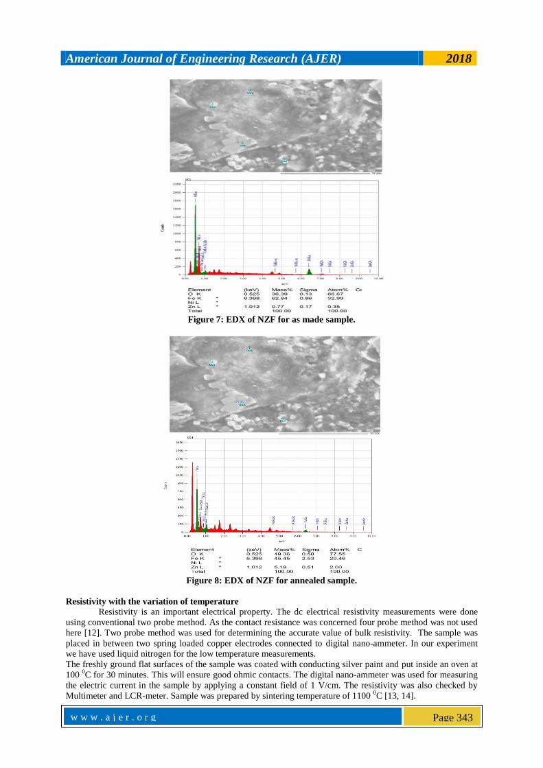
The Energy Dispersive X-ray (EDX) of the sample have been shown in Figure 7 and Figure 8
respectively. Figure 7 is the EDX of the as made sample and Figure 8 is the annealed sample.
We have observed that the percentage composition of different atoms have been changed and the mass of the
elements have also changed due to annealing.
American Journal of Engineering Research (AJER) 2018
w w w . a j e r . o r g
Page 343
Figure 7: EDX of NZF for as made sample.
Figure 8: EDX of NZF for annealed sample.
Resistivity with the variation of temperature
Resistivity is an important electrical property. The dc electrical resistivity measurements were done
using conventional two probe method. As the contact resistance was concerned four probe method was not used
here [12]. Two probe method was used for determining the accurate value of bulk resistivity. The sample was
placed in between two spring loaded copper electrodes connected to digital nano-ammeter. In our experiment
we have used liquid nitrogen for the low temperature measurements.
The freshly ground flat surfaces of the sample was coated with conducting silver paint and put inside an oven at
100 0C for 30 minutes. This will ensure good ohmic contacts. The digital nano-ammeter was used for measuring
the electric current in the sample by applying a constant field of 1 V/cm. The resistivity was also checked by
Multimeter and LCR-meter. Sample was prepared by sintering temperature of 1100 0C [13, 14].

American Journal of Engineering Research (AJER) 2018
w w w . a j e r . o r g
Page 344
The sample was polished by emery paper with grit size of 600 and 800 successively. Then silver paste
was applied to the both sides of the samples along with two thin copper wires of 100 micron diameter. The
resistivity was measured using an Electrometer Keithley model 6517 at room temperature. The resistivity has
been calculated using the formula
LRA
(4)
where 𝜌 is the resistivity, L is the thickness and A is the area of the sample. The variations of electrical
resistivity with temperatures for the sample are shown in Figure 9. It is obvious that the electrical resistivity
decreases with the increasing temperatures, illustrates that the sample exhibits semiconducting behaviour as
usual ferrite characteristics.
Figure 9: Resistivity vs Temperatures.
Equivalent circuit parameters for the sample with varying temperatures
The equivalent circuit parameters with the variation of temperature are shown in Table 2. We have
observed that with the increase of the temperature the resistance and the inductance values are increasing but the
capacitive value is decreasing gradually.
Table 2 Equivalent circuit parameters with temperatures
Temperature
( )
Equivalent
Circuit
Resistance, R (Ω) Inductance, L (µH) Capacitance, C (pF)
-195 301.25 2.0256 11.505
-120 333.44 2.2196 11.496
-90 354.12 2.3312 11.377
-60 367.78 2.4303 11.202
Room 373.42 2.5145 10.812
100 398.62 2.6533 8.7325
120 406.58 2.7842 6.1342
140 411.16 2.8047 5.8874
160 425.39 2.9955 5.7454
180 446.40 3.0417 5.7151
The frequency dependent impedance and its corresponding angle with the variation of temperatures are
also shown in Figure 10 and Figure 11 respectively.

American Journal of Engineering Research (AJER) 2018
w w w . a j e r . o r g
Page 345
Figure 10. Impedance vs frequency
Figure 11. Angle vs frequency
We have also verified the practical results with the theoretical results. And we found very good matching for both
the cases. The simulation has been done in MATLAB with the equivalent circuit parameters which are shown in Figure 12
and 13 respectively.
Figure 12. Theoretical Impedance vs frequency
Figure 13. Theoretical Angle vs frequency
V. CONCLUSION
We can summarize the work with the following points. Microstructure analysis of NZF shows strong
size dependent electrical and magnetic properties. DC resistivity remains constant at low temperature and onset
of decrease occurs around room temperature. Annealing at high temperature has improved the microstructural
properties of the NZF sample. Theoretical equivalent circuit corresponds well with the experimentally observed
electrical parameters. Clear resonance occurs around 30 MHz which makes this material suitable for electronic
device application around this frequency.
ACKNOWLEDGEMENT
The authors would like to express their gratitude to the Islamic University of Technology (IUT)
authority for providing the necessary financial support and permission to carry out this research work. We are
also thankful to the material science laboratory of Bangladesh University of Engineering and Technology
(BUET).

American Journal of Engineering Research (AJER) 2018
w w w . a j e r . o r g
Page 346
Authors Contribution
MTAA performed the experiments and wrote the manuscript, MFAK conceived the idea and guided
the experiments; MRA helped in the experiment, discussed on the results and wrote some parts of the
manuscript. All authors approved the final manuscript.
Competing interest
We declare that we have no competing interest.
REFERENCES [1]. R. Rameshbabu, R. Ramesh, S. Kanagesan, A. Karthigeyan, and S. Ponnusamy, "Synthesis and study of structural, morphological
and magnetic properties of ZnFe2O4 nanoparticles," Journal of Superconductivity and Novel Magnetism, vol. 27, pp. 1499-1502,
2014.
[2]. B. Xue, R. Liu, Z.-D. Xu, and Y.-F. Zheng, "Microwave Fabrication and Magnetic Property of Hierarchical Spherical. ALPHA.-Fe2O3 Nanostructures," Chemistry Letters, vol. 37, pp. 1058-1059, 2008.
[3]. H. Zhang, B. Zhang, G. Wang, X. Dong, and Y. Gao, "The structure and magnetic properties of Zn 1− xNixFe 2 O 4 ferrite
nanoparticles prepared by sol–gel auto-combustion," Journal of magnetism and magnetic materials, vol. 312, pp. 126-130, 2007. [4]. J. Azadmanjiri, "Structural and electromagnetic properties of Ni–Zn ferrites prepared by sol–gel combustion method," Materials
Chemistry and Physics, vol. 109, pp. 109-112, 2008.
[5]. M. Niyaifar, "Effect of Preparation on Structure and Magnetic Properties of ZnFe₂O₄," Journal of Magnetics, vol. 19, pp. 101-105, 2014.
[6]. T. Tsutaoka, "Frequency dispersion of complex permeability in Mn–Zn and Ni–Zn spinel ferrites and their composite materials,"
Journal of Applied Physics, vol. 93, pp. 2789-2796, 2003.
[7]. S. A. Morrison, C. L. Cahill, E. E. Carpenter, S. Calvin, R. Swaminathan, M. E. McHenry, et al., "Magnetic and structural properties of nickel zinc ferrite nanoparticles synthesized at room temperature," Journal of Applied Physics, vol. 95, pp. 6392-6395,
2004.
[8]. S. Zahi, M. Hashim, and A. R. Daud, "Synthesis, magnetic properties and microstructure of Ni–Zn ferrite by sol–gel technique," Journal of magnetism and magnetic materials, vol. 308, pp. 177-182, 2007.
[9]. G. Herrera and M. Pérez-Moreno, "Microstructure dependence of the magnetic properties of sintered Ni–Zn ferrites by solid-state
reaction doped with V2O3," Journal of Materials Science, vol. 47, pp. 1758-1766, 2012. [10]. B. Culity and S. Stock, "Elements of X-ray Diffraction," Reading: Addition-Wesley, 1978.
[11]. M. Ebrahimi, R. R. Shahraki, S. S. Ebrahimi, and S. Masoudpanah, "Magnetic properties of zinc ferrite nanoparticles synthesized
by coprecipitation method," Journal of Superconductivity and Novel Magnetism, vol. 27, pp. 1587-1592, 2014. [12]. M. S. R. Prasad, B. Prasad, B. Rajesh, K. Rao, and K. Ramesh, "Magnetic properties and DC electrical resistivity studies on
cadmium substituted nickel–zinc ferrite system," Journal of magnetism and magnetic materials, vol. 323, pp. 2115-2121, 2011.
[13]. A. A. Hossain, S. Mahmud, M. Seki, T. Kawai, and H. Tabata, "Structural, electrical transport, and magnetic properties of Ni 1− xZnxFe 2 O 4," Journal of magnetism and magnetic materials, vol. 312, pp. 210-219, 2007.
[14]. B. V. Prasad, "Cation distribution, structural and electric studies on cadmium substituted nickel–zinc ferrite," Modern Physics
Letters B, vol. 28, p. 1450155, 2014.
Md. Thesun Al-Amin " Structural and Electrical Properties of Nickel Zinc Ferrite
Nanoparticles.‖ American Journal of Engineering Research (AJER), vol. 7, no. 3, 2018,
pp.338-347.