structural, electronic, optical and transport...
TRANSCRIPT

Structural, Electronic, Optical and Transport Properties of Pristine and Alloyed Ultrathin
Nanowires of Noble Metals
Synopsis for Ph.D. in Physics
Submitted by
Arun Kumar
in
Faculty of Physical SciencesDepartment of Physics
Himachal Pradesh UniversitySummerhill, Shimla-171005
Himachal Pradesh (India)
Presented on 5th January 2013 in
Research Degree Committee meeting of
Physics Department
Supervisor
Dr. P. K. AhluwaliaProfessor
Department of PhysicsHimachal Pradesh University
SummerhillShimla-171005
5th January 2013

Structural, Electronic, Optical and Transport
Properties of Pristine and Alloyed Ultrathin
Nanowires of Noble Metals
1 Introduction
In the last two decades, nanoscience and nanotechnology have initiated muchinterest in fundamental research of the properties of nanomaterials and theirindustrial applications. As a result nanostructured materials as a foundationof nanoscience and nanotechnology, have become the hottest topics of research[2, 3, 49, 147]. Normally, nanostructures are defined as the structures with atleast one dimension less than 100 nm. In this dimension, the number of atomsare countable, making the properties of nanostructures different from those oftheir bulk counterparts due to distinct density of states (DOS) and increasedsurface to volume ratio. According to the number of dimensions less than 100nm, nanostructures can be classified into two-dimensional (2D, nanofilm), one-dimensional (1D, nanotube or nanowire), and zero-dimensional (0D, quantumdot) structures.
1.1 One-dimensional nanostructures
In a 1D nanostructure there is a confinement in two dimensions perpendicu-lar to the longitudinal extent of the structure. This confinement is quantummechanical in nature. Due to the combination of both quantum confinementin the nanoscaled dimensions and the bulk properties in the third dimension,many interesting properties and applications can be expected based on a widevariety of 1D nanostructures. Also it has been observed [1] that 1D nanostruc-tures represent the smallest dimension structure that can efficiently transportelectrical carriers and can be exploited as both the wiring and device elementsin future architectures for functional nanosystems.
Depending on the topology and morphology, the 1D nanostructures can beclassified into following main groups:
• Nanotubes [3].
• Nanowires [4, 5].
• Coaxial cable structures [6].
• Side-by-side biaxial nanowires [7].
• Nanobelts (or nanoribbons) [8].
1

The first three nanostructures listed above have a common characteristic ofcylindrical cross section, biaxial nanowires have the stacking of two parallelnanowires of different materials and nanobelts have a rectangular cross section(belt like morphology). The distinctive geometrical shapes of these 1D nanostuc-tures are important as their mechanical, electrical, optical, and thermal trans-port properties are geometry dependent. To investigate the uniqueness offeredby these shapes, new techniques have been developed to measure the propertiesof individual wire-like structures quantitatively and their structures are wellcharacterized by electron microscopy techniques [2].
1.2 Review of Literature
The quantum confined nanowires have a wide range of applications in electron-ics [60–69], optoelectronics [10–13], thermoelectrics [70, 71], optics [62, 72, 73],chemo and bio-sensing [18, 21, 25–27, 74, 75, 77], magnetic media [78–85], pho-tocatalysis [30–32] and piezoelectronics [33–39] etc. As a result of the rapidprogression of modern nanoelectronics, nanowires (NWs) have begun to drawthe attention of researchers in cross disciplinary areas of physics, chemistry andengineering. In nanoelectronics, nanowires can function as interconnects in thefabrication of integrated circuits [64, 65], resonators [66–69], diodes [9–13, 60],light emitting diodes (LED) [61], multifunctional devices [63], logic gates [18–23]using nanowire field-effect transistors (NW-FETs) [62] and single electron tran-sistors [24]. Their small size and their high electrical conductivity makes themvery attractive for applications in nanoelectronics [76].
Sensing is another area in which the application of nanowires is expected tohave a great impact. Nanowire sensors have been reported, that can detect thepresence of many gases like O2, NO2 and NH3 [74] at very low concentrations.Nanowires also have been used for the detection of ultraviolet light [75] as wellas highly sensitive biological and chemical species [77]. These sensors oftenfunction on the basis of changes in the electrical or physical properties of thenanowires when they come in contact of targeted chemical/biological [74–76]species. The sensing capabilities of nanowires can be controlled by selectivedoping that raises their affinities to certain substances. Also the nanowiresof noble metals particularly have been used as barcode tags for optical readout [86, 87]. Single-crystalline NW have also been used in batteries [47], solarcells [48] and photoelectrochemcal cells [31] for effective charge separation andcollection.
In these areas, NW structures exhibit unique and superior properties com-pared to their bulk counterparts, resulting from 1D confined transport of elec-trons or photons, large surface area, quantum confinement, and excellent me-chanical properties [40–46].
In recent years, long metallic nanowires with well defined structures anda diameter of several nanometers have been fabricated using different meth-ods [88–91]. For example, stable gold nanobridge with 0.8-3 nm in thicknessand 5-10 nm in length has been produced by electron beam irradiation of gold(001) oriented thin film [88]. Also suspended gold nanowire with 6 nm in length
2

and diameter down to 0.6 nm have been made and the novel multishell structurewere observed [91]. In 1998, Ohnishi et. al. [53] used scanning tunneling micro-scope and Yanson et. al. [54] through mechanically break-junction experimentsproduced atomically thin bridge of gold atoms and calculated the conductanceequal to Go = 2e2/h and the interatomic distance was reported as 2.6 A [92].The break-junction experiments have also been performed for Ag [55], Cu [52]
and Pt [52] chains, with conductance nearly 1Go (Go = 2e2
h ) for Cu, Ag and Auand 1.5Go to 2.5Go for Pt chains.
Noble metal nanowires, which is the subject matter of the proposed work,have been drawing a great deal of attention due to their significantly differentstructural, electronic, magnetic, optical and transport properties compared totheir bulk manifestation [49, 50]. The increased surface to volume ratio andincreased density of states (DOS) makes them different from their correspondingbulk materials. Also the DOS does not vanish at subband edges and remainfinite. This makes these materials an interesting and exciting subject to exploreoptical properties. Noble metal nanowires, particularly, can also be used tocreate materials that exhibit negative index of refraction in the near-infraredregion [51]. The finite monoatomic chains of noble metals can be produced bymechanical break junction experiments [52–55] for Cu, Ag, Au and Pt chains.Many innovative experimental studies on one dimensional systems [53,54,56,57],revealing their fascinating properties, have boosted related theoretical research.Depending upon the type of structure, the electronic, magnetic, optical andtransport properties of these systems show interesting variations [58,59].
Very few studies have been made of the properties of metal alloys at the atomicscale (alloyed metal nanowires) [93–98]. In 2002 and 2003, point contact studieswere made of random alloys of a transition metal and a noble metal, namelygold and palladium [93], copper and nickel [94] and gold and platinum [96] fordifferent concentration ratios. In these experiments peak has been found at1Go, that is characteristic of the noble metals, survives for transition metalconcentrations well over 50%. The interpretation for this observation requiresfurther study. There is an evidence for segregation of the noble metals awayfrom the contact under the application of a high bias current [98].
2 Theoretical Background
The universe around us is made of condensed matter i.e. matter whose en-ergy is low enough that it gets condensed to form stable system of atoms andmolecules usually in solid or liquid phases. These atoms and molecules are fur-ther made up of electrons and nuclei. The quantum mechanics has proven to bethe best formulation to describe interacting system of electrons and nuclei. TheSchrodinger equation is the fundamental quantum mechanical equation that de-scribes a system of electrons and nuclei in terms of wave function ψ, which isfundamental entity in quantum mechanics.
3
The systems under study are indeed many electron systems and for a multi-electron system the Schrodinger wave equation can be written as:− ~2
2me
∑i
∇2i −
~2
2MA
∑A
∇2A +
∑A>B
ZAZBe2
4πεoRAB+∑i>j
e2
4πεorij−∑Ai
ZAe2
4πεorAi
ψ = Eψ
Here i and j are indices used for electrons and A and B are the indices used fornuclei. On the left hand side of above equation first two terms represent the ki-netic energy of electrons and nuclei respectively and the following terms describethe inter-nuclear, electron-electron and electron-nuclear Coulomb interaction en-ergies respectively. If we use atomic units i.e. (e = me = ~ = 4πεo = 1), theSchrodinger equation becomes−1
2
∑i
∇2i −
1
2MA
∑A
∇2A +
∑A>B
ZAZB
RAB+∑i>j
1
rij−∑Ai
ZA
rAi
ψ = Eψ (1)
The ultimate aim of any physicist or a chemist for a typical system is to solvethis equation.
However, as Paul Dirac at the dawn of theoretical quantum mechanics has saidthat all the answers of chemistry could be calculated from schrodinger equation[103], but it is the most challenging task to solve this equation analytically.Unfortunately the schrodinger equation can be solved exactly for only a fewsystems such as hydrogen atom and even numerically to systems containingsmall number of electrons [102].
2.1 Approximations
To solve the equation (1) one uses various approximations, which do not sig-nificantly affect the involved physics of the system under study and facilitatemeaningfully the study of variety of many body problems.
2.1.1 Born-Oppenheimer approximation
One of the most simplifying approximation is based upon the idea that mass ofelectron is much smaller than that of the nucleus and thus electrons move muchmore rapidly than nucleus. Thus for a given set of positions of nuclei, electronsadjust almost immediately to movement of nuclei. This is known as Born-Oppenheimer approximation [99]. In other words we can say that forces onboth electrons and nuclei due to their charge are of same order of magnitude, sochanges which occur in their momenta as a result of these forces must also beof the same magnitude. But since nuclei are much more massive than electronsso accordingly they have much smaller velocities. While solving the schrodingerequation given by equation (1), one can assume that nuclei are stationary andsolve it for electronic ground state first and then calculate the energy of thesystem in that configuration and then later solve for nuclear motion. This helpsto separate the electronic and nuclear motion. Furthermore, this allows us toseparate the wavefunction as a product of nuclear and electronic terms. Theelectronic wave function φe(r,R) is solved for a given set of nuclear coordinates
4

Heφe(r,R) = −1
2
∑i
∇2i −
∑A,i
ZA
RAi+∑i>j
1
rijφe(r,R)
= Ee(R)φe(r,R) (2)
and the electronic energy obtained contributes a potential term to the motionof nuclei described by the nuclear wave function φN (R).
HNφN (R) = −∑A
1
2MA∇2
A + Ee(R) +∑A>B
ZAZB
RABφN (R)
= EφN (R) (3)
2.1.2 Independent Electron Approximation
Another approximation called independent electron approximation [120] whichassumes electrons to be non-interacting with each other has quantum manifes-tation because electrons obey Pauli’s exclusion principle. This manifestationof Pauli’s exclusion principle resulted in Hartree-Fock method and allows oneto express total Hamiltonian for N-electron system (H) as summation of singleelectron Hamiltonian (Hi) i.e. H =
∑iHi and total wave function as Slater de-
terminant of single electron wave functions. The slater determinant approxima-tion does not take into account Coulomb Correlation leading to a total electronicenergy different from the exact solution of non-relativistic Schrodinger equationwithin Born-Oppenheimer Approximation. Therefore, Hartree-Fock Energy isalways above the exact energy. This difference is called the Correlation Energy,a term coined by Lowdin [100].
2.2 Density Functional Theory: An Ab initio Approach
To overcome the difficulty of correlation energy and problem of 3N variables,a new approach ‘Density Functional Theory (DFT)’ was adopted for elec-tronic structure calculations. In 1964 Hohenberg and Kohn, showed in a con-ference paper [101] that schrodinger equation (for N electron system containingwave function of 3N variables) could be reformulated as an equation of electrondensity with only three variables. This theory gives approximate solutions toboth Exchange and Correlation Energies. The main objective of DFT is to re-place the many-particle electronic wavefunction with the electronic density asthe basic quantity. Our interest is in solving Schrodinger’s equation by meansof ab initio Density Functional Theory (DFT) as described below.
The term Ab initio used here originates from Latin word which means ‘fromthe beginning’. A method is said to be Ab initio or from first principles if itrelies on basic and established laws of nature without additional assumptionsor special models based upon particular material. Density functional theory(DFT) is an extremely successful ab initio approach to compute properties ofmatter at microscopic scales. DFT is a quantum mechanical modelling methodused in physics to investigate the electronic structure (principally the groundstate) of many-body systems, in particular atoms, molecules, and the condensedphases (bulk, surfaces, chains).
5

The fundamental pillars of density functional theory are two physical theo-rems proved by Kohn and Hohenberg [101,118,119]. The first Hohenberg Kohn(HK) theorem states that: The ground-state energy from Schrodingers equa-tion is a unique functional of the electron density. This theorem provides oneto one mapping between ground state wave function and ground state chargedensity. The first HK theorem is stated as: the ground state charge density canuniquely describe all the ground state properties of system. The fundamentalconcept behind density functional theory is that charge density (3-Dimensional)can correctly describe the ground state of N-particle instead of explicit usage ofwave function (3N-Dimensional) [117]. Thus by using charge density instead ofwave functions a 3N dimensional problem reduces to just a three dimensionalproblem.
The second HK theorem states that: The electron density that minimizes theenergy of the overall functional is the true electron density corresponding to thefull solution of the Schrodinger equation. If the true functional form of energyin terms of density gets known, then one could vary the electron density untilthe energy from the functional is minimized, giving us required ground statedensity. This is essentially a variational principle and is used in practice withapproximate forms of the functional designed by quantum chemists/physiciststo study different types of systems [120]. The simplest possible choice of afunctional can be a constant electron density all over the space.
The total charge density can be written in terms of single particle wave func-tions as:
n(r) =∑µ
ψ∗µ(r)ψµ(r) (4)
An important step towards applying DFT to real systems was taken by Kohnand Sham in 1965 in the form of Kohn-Sham (KS) [119] equations. The Kohn-Sham equation reformulate the Schrodinger equation of interacting electronsmoving in an external ion potential into a problem of non interacting elec-trons moving in an effective potential. The KS equations are defined by alocal effective external potential (called Kohn-Sham potential) in which thenon-interacting particles move. The Kohn-Sham equations have the form(
− ~2
2m∇2 + Veff(r)
)ψµ(r) = εµψµ(r) (5)
where
Veff(r) = V (r) + VH(r) + VXC(r) (6)
The contribution to the total energy here gets divided into two parts. The
first part contains terms: the kinetic energy (− ~2
2m∇2), the hartree potential en-ergy (VH(r)) and classical Coulomb energy (V (r)) and second part contains theexchange correlation energy (VXC(r)) which includes many body and quantumeffects. It is customary to divide the exchange correlation into exchange part(for which there exists an exact expression although computationally expensiveto calculate) and correlation part (which is unknown).
6

Kohn and Sham introduced a set of orbitals from which electron density canbe calculated. These Kohn -Sham orbitals do not in general correspond to actualelectron density. The only connection the Kohn-Sham orbitals have to the realelectronic wave function is that they both give rise to the same charge density.To calculate the kinetic energy term, the Kohn-Sham orbitals are used as shownbelow:
Ts[ρ] =N∑i=1
∫dr ψ∗
µ(r)
(− ~2
2m∇2
)ψµ(r) (7)
On the right-hand side of equation (6) there are three potentials, V , VH , andVXC . The first potential defines the interaction of an electron with differentatomic nuclei present which is basically Coulomb potential. One takes care ofthis term with the help of a trick which replaces Coulomb potential by a Pseu-dopotential [120]. It is well known that since core electrons do not participatein bond formation, it was natural to assume that they can be replaced with apseudo core. That means we have to deal with fewer number of electrons (va-lence electrons). Thus a pseudopotential is an approximation for the full corepotential. How good a pseudopotential is, infact successful for the generatedpseudopotential decided by how well it reproduce the results from all electroncalculations. The effort in generating a pseudopotential lies in the fact that,all electron wave function must match with the pseudo wave function after acertain cut off radii.
The second potential is called the Hartree potential. This potential describesthe Coulomb repulsion between the electron being considered in one of theKohn-Sham equations and the total charge density defined by all electrons in theproblem. The Hartree potential includes a so called self-interaction contributionbecause the electron we are describing in the Kohn-Sham equation is also part ofthe total electron density, so part of VH involves a Coulomb interaction betweenthe electron and itself. The self interaction is unphysical, and the correction forit is one of several effects that are lumped together into the final potential inthe KS equations, VXC , which defines exchange and correlation contributionsto the single electron equations.
To solve KS equation we need Hartree potential which depends upon thecharge density of the system and to know the charge density we need the singleparticle wave functions, which can be obtained only after solving KS equations.Thus the problem reduces to solving a set of self consistent equations. Theyare solved in an iterative way by starting with a trial set of single particle wavefunctions from which Hartree potential is obtained. The solution obtained inthis way is called self consistent solution. The algorithm used to solve it is asgiven in figure 1.
2.3 Local Density Approximation(LDA)
The most important potential term in KS equations is VXC [103] which is usedto describe exchange and correlation effects. Unfortunately, exact form of the
7

Figure 1: Algorithm to solve Kohn Sham equations in DFT Codes
exchange correlation functional whose existence is ensured by the Hohenberg-Kohn theorem is not known. There is only one case of uniform electron gaswhere this functional can be derived exactly as the electron density is constantat all points in space. Therefore, the exchange-correlation potential at each po-sition is set to be obtained from the electron density observed at that position.Since this approximation uses only the local density to define the approximateexchange correlation functional, so it is called the local density approximation(LDA) [121]. Although, LDA gives a way to completely define the Kohn-Shamequations, but these equations do not exactly solve the true Schrodinger equa-tion because the true exchange correlation functional are not being used ratherare always approximately known.
2.3.1 Beyond LDA
Apart from LDA, many other functionals tailored to explain properties of par-ticular systems have been tried for DFT calculations. After LDA, the bestknown class of functional that has been defined is generalized gradient correc-tion (GGA). GGA uses information about the local electron density and alsothe local gradient in the electron density [122]. Though GGA includes morephysical information than LDA, it is not necessary that it must be more ac-curate. There are a large number of distinct GGA functionals depending onthe ways in which information from the gradient of the electron density can beincluded in a GGA functional.
2.3.2 Choosing a Functional
The choice of the functional is the main issue in DFT. The functionals whichuse LDA are CA (Ceperley-Alder) [123] and PW92 [121] (Perdew-Wang-92)and the functionals which use GGA are PBE [122] (Perdew-Burke-Ernzerhof),revPBE [124] (Revised Perdew-Burke-Ernzerhof), PBEsol [125] (Perdew-Burke-Ernzerhof for solids). The most popular functionals are pure density functionalsand hybrid functionals. Altough LDA and GGA are very useful but have prob-lems in certain applications. The main problems with LDA and GGA are theunderestimation of band gaps, failure to describe localized electrons in bothsolids and molecules, absence of Vander Waals interactions, etc. [126].
8
2.3.3 Choosing a Wavefunction
There is another very important aspect of Kohn-Sham equation which lies inits solution described by wave function ψµ(r), which arises when one sets up asimulation. The important question is how does one represent the wavefunctioninside the supercell. The wave function of the full macro-lattice is obtained bycombining these via Bloch functions [127] (k-point sampling). This is knownas basis set [120]. There are four main groups of basis sets used in literaturenamely: plane wave [120], Gaussian [128], augmented [129] and numerical basisset [130–132] and is the starting point of the solution of Kohn-sham equation.The choice of numerical basis sets makes DFT applicable for realistic largesystems.
Atomic orbitals as a basis set have been used for a long time in the electronicstructure calculations of molecules and bulks. Especially, in covalent molecularsystems, one particle wave functions are well described by a linear combinationof atomic orbitals (LCAO) [130] because of the nature of localization in theelectronic states, which is a reason why chemists prefer to use the atomic or-bitals. On the other hand, in the solid-state physics, LCAO has been regardedas a somewhat empirical method such as a tool for an interpolation of elec-tronic structure calculations with a high degree of accuracy. However, duringthe last decade, LCAO has been attracting much interest from different points ofview, since great efforts have been made not only for developing order N (O(N))methods of the eigen value problem, but also for making efficient and accuratelocalized orbitals as a basis set being suitable for O(N) [130–132] methods toextend the applicability of density functional theories (DFT) to realistic largesystems. Once atomic orbitals are chosen one can expand a Kohn-Sham (KS)orbital ψµ of a given system using these atomic orbitals φiα in a form known aslinear combination of atomic orbitals (LCAO) as:
ψµ(r) =∑iα
cµ,iαφiα(r− ri) (8)
where i is a site index, α ≡ (plm) is an organized orbital index, and φiα(r) ≡Ylm(θ, φ)Ripl(r). Here Ripl is the radial wave function, which depends on angu-lar momentum quantum number l, site index i, and a multiplicity index p andYlm spherical wave function. The spherical wave function is well defined (fixedshape), also one can play with shape (number of atomic orbitals per atom),range (spatial extension of the orbitals) and shape of the radial part of wavefunction.
Density functional theory of electronic structure is widely and successfullyapplied in simulations throughout engineering and sciences. However, for manypredicted properties, there are known failures [103] that can be traced to thedelocalization error and static correlation error of commonly used approxima-tions. A clear understanding of the errors from the most basic principles hasenabled the development of functionals to open new frontiers for applications ofDFT.
9

2.4 DFT and Structural Properties
The most basic type of DFT calculation is the computation of the structuralproperties of the system under study. One can begin with electron density, thenuse the trial density to define the effective potential. The Kohn-sham equationswith this effctive potential are solved self consistently till self consistent solu-tion for electron density is obtained as stated earlier. The electron density soobtained has been used to calculate the ground state energy for a given system.One can use various methods for structure optimization. Congugate gradientis one such structure optimization method. In these calculations one can allowthe position of atoms to change keeping the shape of the supercell constant orcan allow both atoms and supercell to change. The structure corresponding tominimum energy tell us about the structural parameters (for example latticetype, lattice constant, bond length, bond angle etc.).
2.5 DFT and Electronic Properies
One of the primary quantities used to describe the electronic state of a materialis the electronic density of states (DOS):
ρ(E)dE = number of electronic states with energies in the interval (E,E+dE)
Once the DFT calculations have been performed, the electronic DOS canbe determined by integrating the resulting electron density in k-space. There isanother very important electronic property known as band structure, that canalso be estimated using DFT. The DFT does not gives us exact band structure,but gives us Kohn-Sham band structure. The Kohn-Sham band structure isgenerally one-electron band structure and which is the dispersion of the energylevels n as a function of k in the Brillouin zone. The Kohn-Sham eigenvaluesand eigenstates are not one-electron energy states for the electron in the solid.However, it is common to interpret the solutions of Kohn-Sham equations asone-electron states: the result is often a good representation, especially con-cerning band dispersion. The main problem with the band structure is theunderestimation of band gap. Band gap error is not due to LDA, but can beattributed to the discontinuity in the exact Vxc [104–107]. DFT is, in principle,an exact theory to reproduce and predict ground state properties (e.g., the totalenergy, the atomic structure, etc.). However, DFT is not a theory to addressexcited state properties, such as the band plot of a solid. Hence, in principle,Kohn-Sham based DFT is not a band theory, i.e., not a theory suitable for cal-culating bands and band-plots. In principle time-dependent DFT can be usedto calculate the true band structure although in practice this is often difficult.
2.6 DFT and Dielectric Properties
DFT also have been used to perform dielectric properties calculations of ma-terials. The formula used for calculating dielecric function [108, 110, 111] wasgiven as:
ε(ω, q) = 1 +8πe2
Ωq2
∑k,n,m
|〈k+q, n|eiqr|k,m〉|2(fk,m − fk+q,n)
Ek,m − Ek+q,n + ~ω + iδ(9)
10
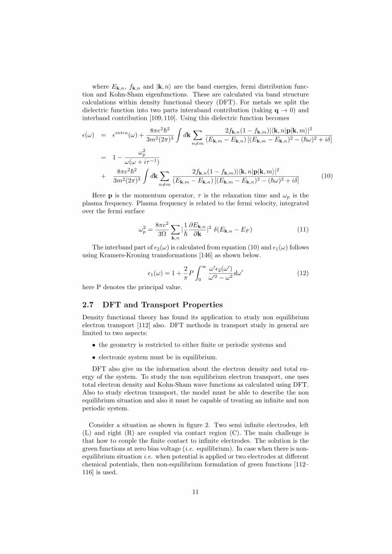
where Ek,n, fk,n and |k, n〉 are the band energies, fermi distribution func-tion and Kohn-Sham eigenfunctions. These are calculated via band structurecalculations within density functional theory (DFT). For metals we split thedielectric function into two parts interaband contribution (taking q → 0) andinterband contribution [109,110]. Using this dielectric function becomes
ε(ω) = εintra(ω) +8πe2~2
3m2(2π)3
∫dk
∑n 6=m
2fk,n(1− fk,m)|〈k, n|p|k,m〉|2
(Ek,m − Ek,n) [(Ek,m − Ek,n)2 − (~ω)2 + iδ]
= 1−ω2p
ω(ω + iτ−1)
+8πe2~2
3m2(2π)3
∫dk
∑n6=m
2fk,n(1− fk,m)|〈k, n|p|k,m〉|2
(Ek,m − Ek,n) [(Ek,m − Ek,n)2 − (~ω)2 + iδ](10)
Here p is the momentum operator, τ is the relaxation time and ωp is theplasma frequency. Plasma frequency is related to the fermi velocity, integratedover the fermi surface
ω2p =
8πe2
3Ω
∑k,n
|1~∂Ek,n
∂k|2 δ(Ek,n − EF ) (11)
The interband part of ε2(ω) is calculated from equation (10) and ε1(ω) followsusing Kramers-Kroning transformations [146] as shown below.
ε1(ω) = 1 +2
πP
∫ ∞
0
ω′ε2(ω′)
ω′2 − ω2dω′ (12)
here P denotes the principal value.
2.7 DFT and Transport Properties
Density functional theory has found its application to study non equilibriumelectron transport [112] also. DFT methods in transport study in general arelimited to two aspects:
• the geometry is restricted to either finite or periodic systems and
• electronic system must be in equilibrium.
DFT also give us the information about the electron density and total en-ergy of the system. To study the non equilibrium electron transport, one usestotal electron density and Kohn-Sham wave functions as calculated using DFT.Also to study electron transport, the model must be able to describe the nonequilibrium situation and also it must be capable of treating an infinite and nonperiodic system.
Consider a situation as shown in figure 2. Two semi infinite electrodes, left(L) and right (R) are coupled via contact region (C). The main challenge isthat how to couple the finite contact to infinite electrodes. The solution is thegreen functions at zero bias voltage (i.e. equilibrium). In case when there is non-equilibrium situation i.e. when potential is applied or two electrodes at differentchemical potentials, then non-equilibrium formulation of green functions [112–116] is used.
11

Figure 2: A model to study transport properties
3 Computational Method
Today many open source and proprietary computer codes are available whichprovide a way to calculate and study various properties of materials using den-sity functional theory. These codes differ in terms of their implementationsused to solve KS equations. Depending on how atomic electrons are treatedthey are termed as full potential (FP-Wien2k [133] and ELK [134]), pseudopo-tential (SIESTA [135], CASTEP [136]), atomic sphere approximation (ASA-SPRKKR [137]) or Muffin tin (LMTO [138]) based. They are also classifieddepending upon what basis set is used to expand wave function. Various meth-ods use plane wave (PW: Quantum Essperso, ABINIT, VASP, CASTEP), aug-mented plane wave (APW: ELK, Wien2k, EXCITING) or localised atomic or-bitals as basis sets (SIESTA, FPLO) [139]. We in our study of nanowires havedecided to use SIESTA (Spanish Initiative for Electronic Simulations on Thou-sands of Atoms) code which is an open source code, using atomic orbitals andis very efficient, easy to run on a quad core machine in parallel mode. In thefollowing, is given a brief description of SIESTA code which we are using to cal-culate the structural, electronic, optical and transport properties of Nanowiresusing DFT.
3.1 SIESTA Code
SIESTA (Spanish Initiative for Electronic Simulations on Thousands of Atoms)is a calculation method and computer code which solves problems of condensedmatter using density functional theory (DFT). These problems are, generally,related to ground-state properties. Energy/volume curves, phase diagrams (e.g.,magnetic ones), phonons are all related to ground-state structural properties andab initio molecular dynamics. It uses norm-conserving pseudopotentials in theirfully nonlocal (Kleinman-Bylander) form. As stated above atomic orbitals areused as a basis set, allowing inclusion of unlimited multiple-zeta and angularmomenta, polarization and off-site orbitals. This is an efficient code to performDFT calculations on systems containing large number of atoms.
SIESTA falls into category of methods with atom-centered basis sets. It meansthat it allows choice of big unit cell volumes. For doing calculations with largesystems, we have to only optimize basis set.
12

3.2 Possibilities with SIESTA
SIESTA can be used to study the structural (lattice constant, bulk modulus,cohesive energy, phonon spectrum), electronic (band structure, DOS), magnetic(magnetic moment) and optical (real and imaginary part of dielectric function)properties of Bulk materials, surfaces, clusters, CNT, nanowires, liquids (radialdistribution function), biomolecules. It can also be used to study the transportproperties of nanosystems at zero bias voltage and at some finite bias voltage.In other words we can say that SIESTA is a very efficient method and a tool tostudy various properties of condensed matter.
3.3 Structural Properties using SIESTA
Several options for structural optimization have been implemented in SIESTA.CG [140](Coordinate optimization by conjugate gradients), Broyden [141] (Co-ordinate optimization by a modified Broyden scheme) and FIRE (Coordinateoptimization by Fast Inertial Relaxation Engine (FIRE) [142]. These differentrelaxation methods moves the atoms (and optionally the cell vectors) tryingto minimize the forces (and stresses) on them. One can calculate the struc-tural parameters (lattice constant, bond length and bond angle with the helpof visualization code known as Xcrysden [143]) of the relaxed structure
3.4 Electronic Properties using SIESTA
The band structure calculations have been performed after the geometry op-timization. k-mesh is a very important parameter for doing band structurecalculations. However one needs to check the convergence, in terms of graduallyincreasing the k-mesh density.
3.5 Dielectric Properties using SIESTA
Other important feature of SIESTA code is to study dielectric properties ofthe materials. The dielectric properties calculations in the code is performedby using first-order time-dependent perturbation theory [144, 145] to find thedipolar transition matrix elements between occupied and unoccupied single-electron eigenstates as implemented in SIESTA, in which the exchange andcorrelation effects are taken care of by plugging, the self consistent ground stateDFT energies and eigenfunctions into the dipolar transition matrix elements.Thus the imaginary part of the dielectric function ε2 is obtained, which canbe further used to calculate real part ε1 of dielectric function and reflectancespectra with the help of Kramers-Kronig transformations [146]. The electronenergy loss spectra (EELS) can be calculated from real and imaginary parts ofdielectric functions as
Im
− 1
ε(ω)
=
ε2(ω)
ε21(ω) + ε22(ω)(13)
.Using real and imaginary part of dielectric function, other optical properties
like refractive index (n), extinction coefficient(κ), reflectance (R) etc. can alsobe calculated using following relations:
13

n =
√√ε21 + ε22 + ε1
2
κ =
√√ε21 + ε22 − ε1
2
R =n+ iκ− 1
n+ iκ+ 1(14)
3.6 Transport Properties using SIESTA
One of the most interesting features of SIESTA is availability of a module to cal-culate transport properties particularly of nano-systems, known as TranSiesta.It is based on DFT and Non-equilibrium Green Function [112,114,115] (NEGF)method which can be used for both structure relaxation and conductance cal-culations. Using TranSiesta, one can calculate electronic transport propertiessuch as, zero bias conductances and the I-V characteristics, of a nanoscale sys-tem in contact with two electrodes at different electrochemical potentials. Heredensity functional theory (DFT) is used for the electronic structure calculationsand then combined with non-equilibrium Greens function (NEGF) theory forthe quantum transport. Various steps used by TranSIESTA are as follows:
• Calculation of the bulk electrodes, to get H (hamiltonian), charge density(ρ), and Self-energies.
• Calculation for the open system
1. Reads the electrode data.
2. Builds H from ρ.
3. Solves the open problem using Non-equilibrium Greens Functions.
4. Builds new ρ.
5. If ρ self consistent, then stop, otherwise go to step 2.
• Postprocessing tool, which computes T(E), I and V.
In other words we can say that this method is based on non equilibriumGreens functions (NEGF), that are constructed using the density functionaltheory Hamiltonian obtained from a given electron density. A new density iscomputed using the NEGF formalism, which closes the DFT-NEGF self consis-tent cycle.
4 Motivations and Research Objectives
The structural, electronic and magnetic properties of transition metals and no-ble metals NWs (free standing) with different topologies (linear, ladder, zigzag,double zigzag) [147–151] have been studied extensively in the past. But thereis a dearth of reports on optical properties. These properties can prove to bea useful tool in analyzing the electronic properties of bulk and low-dimensional
14

structures. Also their study equips one with a better understanding of theelectronic structure. Literature shows that the optical studies have mainly con-centrated on NWs of semiconductor materials. We are particularly interestedin the ultrathin NWs of the noble metals in pristine and alloyed form. Alsothe alloyed nanowires have many applications in electronics and optoelectron-ics [86,152]. But there is lack of theoretical/computational reports on electronic,optical and transport properties of alloyed ultrathin nanowires of noble metals.
Our main objective is to study the structural, electronic, optical and transportproperties of pristine and alloyed free standing ultrathin nanowires of noblemetals with different topologies and morphologies.
5 Work Done So Far
Till date we have studied the bulk properties (structural, electronic and di-electric) of FCC structured noble metal namely Cu, Ag, Au and Pt [58]. Wehave also studied the structural, electronic and dielectric properties of pristinefree standing noble metal (Cu, Ag, Au and Pt) ultrathin nanowires in differenttopologies.
Dielectric functions of bulk noble metals is in good agreement with exper-imentally measured data. The binding energy has been found largest for Ptnanowires and smallest for Ag nanowires. Dimer topology of Ag wire and lin-ear topology of the Ag and Cu wires are found nearly semi metallic in natureas compared to metallic nature of all other topologies of studied wires. Thepartial DOS of all the studied topologies of noble metals have been found tohave contribution mainly from ‘d’orbitals, however, significant contribution from‘s’orbitals have been found to come from linear and dimer topologies of all thenoble metals. The pronounced DOS has been found to increase in nanowires ascompared to their bulk counterparts. Ballistic conductance increases for ladderand zigzag topology of Cu, Ag and Au as compared to other topologies, while itremains same for all the topologies of Pt wire. The reflectance edge for all thestudied topologies of wires is found in infrared region except ladder topology ofPt for which reflectance edge has been found near visible region. The percentagedecrease in the position of reflectance edge w.r.t. bulk has been found largestfor Pt ultrathin nanowires among all the studied ultrathin nanowires of noblemetals. Dielectric properties of nanowires has been found to change significantlywith the topology, therefore, suggesting that the optical properties can be usedas a tool for characterization of the nanowires.
6 Future Plan of Work
In future we will focus on structural, electronic and optical properties of freestanding alloyed nanowires of noble metals with different topologies (linear,ladder, double zigzag). We will compare the results with the correspondingpristine nanowires. Further we will study the transport properties of of these freestanding nanowires (both pristine and alloyed nanowire) using TRANSIESTAa module in SIESTA to study electron transport of nanowires.
15
References
[1] J. Hu, T. W. Odom, C. M. Lieber, Acc. Chem. Res. 32 (1999) 435
[2] Y. Takai, T. Kawasaki, Y. Kimura, T. Ikuta, R. Shimizu, Phys. Rev. Lett.87 (2001) 106105.
[3] S. Iijima, Nature 354 (1991) 56
[4] A. M. Morales, C. M. Lieber, Science 279 (1998) 208.
[5] D. P. Yu, Z. G. Bai, Y. Ding, Q. L. Hang, H. Z. Zhang, J. J. Wang, Y. H.Zou, W. Qian, G. C. Xiong, H. T. Zhou, S. Q. Feng, Appl. Phys. Lett. 72(1998) 3458
[6] Y. Zhang, K. Suenaga, C. Colliex, S. Iijima, Science 281 (1998) 973
[7] Z. L. Wang, Z. R. Dai, Z. G. Bai, R. P. Gao, J. Gole, Appl. Phys. Lett. 77(2000) 3349.
[8] Z. W. Pan, Z. R. Dai, Z. L. Wang, Science 291 (2001) 1947
[9] F. Qian, S. Gradecak, Y. Li, C. Y. Wen, C. M. Lieber, Nano Lett. 5 (2005)2287.
[10] K. Tomioka, J. Motohisa, S. Hara, K. Hiruma, T. Fukui, Nano Lett. 10,(2010) 1639.
[11] S. K. Lee, T. H. Kim, S. Y. Lee, K. C. Choi, P. Yang, Philos. Mag. 87(2007) 2105.
[12] C. Mazuir W. V. Schoenfeld, J. Nanophotonics 1 (2007) 013503.
[13] S. Xu, C. Xu, Y. Liu, Y. F. Hu, R. S. Yang, Q. Yang, J. H. Ryou, H. J.Kim, Z. Lochner, S. Choi, R. Dupuis, Z. L. Wang, Adv. Mater. 22 (2010)4749.
[14] S. Vandenbrouck, K. Madjour, D. Theron, Y. J. Dong, Y. Li, C. M. Lieber,C. Gaquiere, IEEE Electron Device Lett. 30 (2009) 322.
[15] Y. Li, J. Xiang, F. Qian, S. Gradecak, Y. Wu, H. Yan, H. Yan, D. A. Blom,C. M. Lieber, Nano Lett. 6 (2006) 1468.
[16] X. C. Jiang, Q. H. Xiong, S. Nam, F. Qian, Y. Li, C. M. Lieber, Nano Lett.7 (2007) 3214.
[17] M. T. Bjork, O. Hayden, H. Schmid, H. Riel, W. Riess, Appl. Phys. Lett.90 (2007) 142110.
[18] G. H. Yu, C. M. Lieber, Pure Appl. Chem. 82 (2010) 2295.
[19] N. A. Kotov, J. O. Winter, I. P. Clements, E. Jan, B. P. Timko, S.Campidelli, S. Pathak, A. Mazzatenta, C. M. Lieber, M. Prato, R. V.Bellamkonda, G. A. Silva, N. W. S. Kam, F. Patolsky, L. Ballerini, Adv.Mater. 21 (2009) 3970.
16
[20] X. C. Jiang, J. S. Hu, L. A. Fitzgerald, J. C. Biffinger, P. Xie, B. R.Ringeisen, C. M. Lieber, Proc. Natl. Acad. Sci. U.S.A. 107 (2010) 16806.
[21] H. Yan, H. S. Choe, S. W. Nam, Y. J. Hu, S. Das, J. F. Klemic, J. C.Ellenbogen, C. M. Lieber, Nature 470 (2011) 240.
[22] B. Z. Tian, T. Cohen-Karni, Q. A. Qing, X. J. Duan, P. Xie, C. M. Lieber,Science 329 (2010) 830.
[23] S. Nam, X. C. Jiang, Q. H. Xiong, D. Ham, C. M. Lieber, Proc. Natl. Acad.Sci. U.S.A. 106 (2009) 21035.
[24] C. Thelander, T. Martensson, M. T. Bjork, B. J. Ohlsson, M. W. Larsson,L. R. Wallenberg, L. Samuelson, Appl. Phys. Lett. 83 (2003) 2052.
[25] X. D. Wang, C. J. Summers, Z. L. Wang, Nano Lett. 4 (2004) 423.
[26] J. Zhou, Y. Ding, S. Z. Deng, L. Gong, N. S. Xu, Z. L. Wang, Adv. Mater.17 (2005) 2107.
[27] A. Ponzoni, E. Comini, G. Sberveglieri, J. Zhou, S. Z. Deng, N. S. Xu, Y.Ding, Z. L. Wang, Appl. Phys. Lett. 88 (2006) 203101.
[28] A. I. Hochbaum, P. D. Yang, Chem. Rev. 110 (2010) 527.
[29] M. Fardy, A. I. Hochbaum, J. Goldberger, M. M. Zhang, P. D. Yang, Adv.Mater. 19 (2007) 3047.
[30] J. Shi, Y. Hara, C. L. Sun, M. Anderson, X. D. Wang, Nano Lett. 11 (2011)3413.
[31] S. W. Boettcher, J. M. Spurgeon, M. C. Putnam, E. L. Warren, D. B.Turner-Evans, M. D. Kelzenberg, J. R. Maiolo, H. A. Atwater, N. S. Lewis,Science 327 (2010) 185.
[32] M. D. Kelzenberg, S. W. Boettcher, J. A. Petykiewicz, D. B. Turner Evans,M. C. Putnam, E. L. Warren, J. M. Spurgeon, R. M. Briggs, N. S. Lewis,H. A. Atwater, Nature Mater. 9 (2010) 239.
[33] X. D. Wang, J. H. Song, J. Liu, Z. L. Wang, Science 316 (2007) 102.
[34] C. T. Huang, J. H. Song, W. F. Lee, Y. Ding, Z. Y. Gao, Y. Hao, L. J.Chen, Z. L. Wang, J. Am. Chem. Soc. 132 (2010) 4766.
[35] Y. Qin, X. D. Wang, Z. L. Wang, Nature 451 (2008) 809.
[36] Z. L. Wang, Nano Today 5 (2010) 540.
[37] Z. L. Wang, J. Phys. Chem. Lett. 1 (2010) 1388.
[38] C. T. Huang, J. H. Song, C. M. Tsai, W. F. Lee, D. H. Lien, Z. Y. Gao,Y. Hao, L. J. Chen, Z. L. Wang, Adv. Mater. 22 (2010) 4008.
[39] G. C. Yi, C. R. Wang, W. I. Park, Semicond. Sci. Technol. 20 (2005) S22.
[40] C. M. Lieber, Z. L. Wang, MRS Bull. 32 (2007) 99.
17

[41] E. Garnett, P. D. Yang, Nano Lett. 10 (2010) 1082.
[42] R. X. Yan, D. Gargas, P. D. Yang, Nat. Photonics 3 (2009) 569.
[43] B. Tian, T. J. Kempa, C. M. Lieber, Chem. Soc. Rev. 38 (2009) 16.
[44] S. A. Dayeh, A. V. Gin, S. T. Picraux, Appl. Phys. Lett. 98 (2011) 163112.
[45] Y. Cui, X. F. Duan, J. T. Hu, and C. M. Lieber, J. Phys. Chem. B 104(2000) 5213.
[46] C. M. Lieber, Nano Lett. 2 (2002) 81.
[47] M. Law, L. E. Greene, J. C. Johnson, R. Saykally, P. D. Yang, NatureMater. 4 (2005) 455.
[48] C. K. Chan, H. L. Peng, G. Liu, K. McIlwrath, X. F. Zhang, R. A. Huggins,and Y. Cui, Nat. Nanotechnol. 3 (2008) 31.
[49] B. Bhushan, Spriger Handbook of Nanotechnology, Volume 2, second ed.,Springer, Heidelberg, 2006.
[50] M. Springborg and Y. Dong, Handbook of Metal Physics: MetallicChains/Chains of Metals, first ed., Elsevier, Netherlands, 2007.
[51] X. Hu and C. T. Chan, Appl. Phys. Lett. 85 (2004) 1520
[52] R.H.M. Smit, C. Untiedt, A.I. Yanson, J.M. van Ruitenbeek, Phys. Rev.Lett. 87 (2001) 266102
[53] H. Ohnishi, Y. Kondo, K. Takayanagi, Nature 395 (1998) 780
[54] A.I. Yanson, G. R. Bollinger, H.E. van den Brom, N. Agraıt, and J.M. vanRuitenbeek, Nature 395 (1998) 783
[55] N. Agraıt, A.L. Yeyati, J.M. van Ruitenbeek, Phys. Reps. 377 (2003) 81
[56] V. Rodrigues, T. Fuhrer, D. Ugarte, Phys. Rev. Lett. 85 (2000) 4124
[57] P. Gambardella, A. Dallmeyer, K. Maiti, M. C. Malagoli, W. Eberhardt,K. Kern, C. Carbone, Nature (London) 416 (2002) 301
[58] A. Kumar, A. Kumar, P.K. Ahluwalia, Physica E 46 (2012) 259
[59] P. Sen, S. Ciraci, A. Buldum, I. P. Batra, Phys. Rev. B 64 (2001) 195420.
[60] Y. Huang, X. Duan, Y. Cui, L. J. Lauhon, K. H. Kim, C. M. Lieber, Science294 (2001) 1313
[61] X. Duan, Y. Huang, Y.Cui, J. Wang, C. M. Lieber, Nature 409 (2001) 66
[62] M. S. Gudiksen, L. J. Lauhon, J. Wang, D. Smith, C. M. Leiber, Nature415 (2002) 617
[63] M. Mongillo, P. Spathis, G. Katsaros, P. Gentik, S. De Franceschi, NanoLett. 12 (2012) 3074
18

[64] N. Kharche, S. R. Manjari, Y. Zhou, R. E. Gear, S. K. Nayak, J. Phys.Condens. Matter 23 (2011) 085501
[65] J. Song, W. Dongmok, M. C. McAlpine, R. S. Friedman, W. Yue, C. M.Lieber, Nano Letters 4 (2004) 915
[66] S. Perisanu, P. Vincent, A. Ayari, M. Choueib, S. T. Purcell, M. Bechelany,D. Cornu, App. Phys. Lett. 90 (2007) 43113
[67] Z. L. Wang, G. R. Ping, P. Z. Wei, D. Z. Rong, Advanced EngineeringMaterials 3 (2001) 657
[68] A. Shik, H. E. Ruda, I. G. Currie, J. Appl. Phys. 98 (2005) 94306
[69] A. Husain, J. Hone, H. W. C. Postma, X. M. H. Huang, T. Drake, M.Barbic, A. Scherer, M. L. Roukes, App. Phys. Lett. 83 (2003) 1240
[70] J. P. Heremans, C. M. Thrush, Phys. Rev. B 59 (1999) 12579
[71] J. P. Heremans, C. M. Thrush, D. T. Morelli, M. C. Wu, Phys. Rev. Lett.88 (2002) 216801
[72] X. Duan, Y. Huang, Y. Cui, J. Wang, and C. M. Lieber, Nature 409 (2001)66
[73] M. H. Huang, S. Mao, H. Feick, H. Yan, Y. Wu, H. Kind, E. Weber, R.Russo, P. Yang, Science 292 (2001) 1897
[74] Daihua Zhang, Chao Li, Xiaolei Liu, Song Han, Tao Tang, Chongwu Zhou,Appl. Phys. Lett. 83 (2003) 1845
[75] H. Kind, Adv. Materials 14 (2002) 158
[76] Y. Cui, C. Lieber, Science 291 (2001) 851
[77] Y. Cui, Q. Wei, H. Park, C. Lieber, Science 293 (2001) 1289
[78] H. Zeng, M. Zheng, R. Skomski, D. J. Sellmyer, Y. Liu, L. Menon, S.Bandyopadhyay, J. Appl. Phys. 87 (2000) 4718
[79] A. Bala, T. Nautiyal, S. Auluck, Journal of Magnetism and Magnetic Ma-terials 321 (2009) 1856
[80] T. Thurn-Albrecht, J. Schotter, G. A. Kastle, N. Emley, T. Shibauchi, L.Krusin-Elbaum, K. Guarini, C. T. Black, M. T. Tuominen, T. P. Russell,Science 290 (2000) 2126
[81] R. Moradian, A. Fathalian, Nanotechnology 17 (2006) 1835
[82] X. Ma, Y. Cai, N. Lun, S. Wen, Nanotube-based Devices 772 (2003) 87
[83] E. Borowiak-Palen, E. Mendoza, A. Bachmatiuk, M. H. Rummeli, T. Gem-ming, J. Nogues, V. Skumryev, R. J. Kalenczuk, T. Pichler, S. R. P. Silva,Chem. Phys. Lett. 421 (2006) 129
[84] Y.-L. Mao, X.-H. Yan, Y. Xiao, Nanotechnology 16 (2005) 3092
19

[85] M. Weissmann, G. Garcia, M. Kiwi, R. Ramirez, Phys. Rev. B 70 (2004)201401
[86] S. Nicewarner-Pena, R. G. Freeman, He L. Reis, D. Pena, I. Walton, R.Cromer, C. K. M. Natan, Science 294 (2001) 137
[87] H. He, N. J. Tao, Encyclopedia of Nanoscience and Nanotechnology, VolX, American Scientic Publishers, North Lewis Way, 2004.
[88] Y. Kondo, K. Takayanagi, Phys. Rev. Lett. 79 (1997) 3455.
[89] I. Lisiecki et al, Phys. Rev. B 61 (2000) 4968.
[90] W. S. Yun et al, J. Vac. Sci. Technol. A 18 (2000) 1329.
[91] Y. Kondo, K. Takayanagi, Science 289 (2000) 606.
[92] G. Untiedt, A.I. Yanson, R. Grande, G. Rubio-Bollinger, N. Agraıt, S.Vieira, J.M. van Ruitenbeek, Phys. Rev. B 66 (2002) 085418
[93] A. Enomoto, S. Kurokawa, and A. Sakai, Phys. Rev. B 65 (2002) 125410.
[94] D.J. Bakker, Y. Noat, A.I. Yanson, and J.M. van Ruitenbeek, Phys. Rev.B 65 (2002) 235416.
[95] N. Agraıt, A. L. Yeyatib, J. M. van Ruitenbeek, Phys. Rep. 377 (2003) 81
[96] A. Anaya, A.L. Korotkov, M. Bowman, J. Waddell, D. Davidivic,Nanometer-scale metallic grains connected with atomic-scale conductors,preprint (2002). http://arXiv.org/abs/cond-mat/0210620.
[97] A. Enomoto, S. Kurokawa, A. Sakai, Phys. Rev. B 65 (2002) 125410
[98] J.W.T. Heemskerk, Y. Noat, D.J. Bakker, J.M. van Ruitenbeek, B.J. Thi-jsse, P. Klaver, A current induced transition in atomic-size contacts ofmetallic alloys, preprint (2002). http://arXiv.org/abs/cond-mat/0209577.
[99] T. J. Gil, S. Shi, A. Askar, H. A. Rabitz, Phys. Rev. A 45 (1992) 6479.
[100] P.-O. L owdin, Phys. Rev. 97 (1955) 1474.
[101] P. Hohenberg, W. Kohn, Phys. Rev. 136 (1964) B864.
[102] L. I. Schiff, Quantum Mechanics, Tata McGraw Hill, 3rd ed.
[103] A. E. Mattsson, Science 298 (2002) 759.
[104] L. J. Sham, M. Schlter, Phys. Rev. Lett. 51 (1983) 1888.
[105] L. J. Sham, M. Schlter, Phys. Rev. B 32 (1985) 3883.
[106] J. P. Perdew and M. Levy, Phys. Rev. Lett. 51 (1983) 1884.
[107] R. W. Godby, M. Schluter, L. J. Sham, Phys. Rev. Lett. 56 (1986) 2415.
[108] F. Knider, J. Hugel, A. V. Postnikov, J. Phys.: Condens. Matter 19 (2007)196105.
20

[109] F. Wooten, Optical Properties of Solids, Academic Press (1972).
[110] P. B. Johnson, R. W. Christy, Phys. Rev. B 6 (1972) 4370-4279.
[111] A. Y-C. Yu, W. E. Spicer, Phys. Rev. 171 (1968) 834-835.
[112] K. Stokbro, J. Taylor, M. Brandbyge, P. Ordejon, Ann. N.Y. Acad. Sci.1006 (2003) 212.
[113] M. Brandbyge, J. L. Mozos, P. Ordejon, J. Taylor, K. Stokbro, Phys. Rev.B 65 (2002) 165401.
[114] M. Buttiker, Y. Imry, R. Landauer, and S. Pinhas, Phys. Rev.B 31 (1985)6207.
[115] S. Datta, Electronic Transport in Mesoscopic Systems, Cambridge Uni.Press, 1997
[116] S. Datta, Quantum Transport: Atom to Transistor, Second ed., Cam-bridge University Press 2005
[117] David S. Sholl and Janice A. Steckel, Density Functional Theory: A Prac-tical Introduction, Willey, 2009
[118] W. Kohn, Nobel Lecture: Electronic Structure of Matter-Wave Functionsand Density Functionals, Rev. Mod. Phys. 71, 1253 (1999)
[119] W. Kohn and L. J. Sham, Phys. Rev. 140, A1133 (1965)
[120] M. C. Payne, M. P. Teter, D. C. Allen, T. A. AriasandJ. D. Joannopoulos,Rev. Mod. Phys. 64 (1992) 1045
[121] John P. Perdew and Yue Wang Phys. Rev. B 45 (1992) 13244.
[122] John P. Perdew, K. Burke, andM. Ernzerhof, Phys. Rev. Lett. 77, 3865(1996)
[123] Perdew, Zunger, PRB 23 (1981) 5075.
[124] Y. Zhang, W. Yang, PRL 80 (1998) 890.
[125] J. P. Perdew, A. Ruzsinszky, G. I. Csonka, O. A. Vydrov, G. E. Scuseria,L. A. Constantin, X. Zhou, K. Burke, Phys. Rev. Lett. 100 (2008) 136406-136409.
[126] A. J. Cohen, P Mori-Sanchez, W. Yang, Science, 321 (2008) 792
[127] C. Kittel, Introduction to Solid State Physics, seventh ed., Wiley, NewYork, 1996.
[128] L. Burnelle, J. J. Kaufman, J. Chem. Phys. 43 (1965) 3540.
[129] P. E. Blochl, Phys. Rev. B 50 (1994) 17953.
[130] E. Artacho, D. Sanchez-Portal, P. Ordejon, A. Garcıa, J. M. Soler, Phys.Stat. Sol. (b) 215 (1999) 809. (1999).
21

[131] P. Ordejon, D. A. Drabold, M. P. Grumbach, R. M. Martin, Phys. Rev.B 48 (1993) 14646.
[132] P. Ordejon, E. Artacho, J. M. Soler, Phys. Rev. B 53, (1996) 10441.
[133] P. Blaha et. al. WIEN2k, An Augmented Plane Wave+Local Orbitals Pro-gram for Calculating Crystal Properties, Technical University of Vienna,Vienna (2001)
[134] http://elk.sourceforge.net/
[135] http://www.uam.es/siesta
[136] http://www.castep.org/
[137] http://olymp.cup.uni-muenchen.de/ak/ebert/SPRKKR
[138] http://www2.fkf.mpg.de/andersen/
[139] Richard M. Martin, Electronic Structure: Basic Theory and PracticalMethods Cambridge University Press (2004)
[140] J. R. Shewchuk, An Introduction to the Conjugate Gradient MethodWithout the Agonizing Pain, School of Computer Science, Carnegie MellonUniversity, Pittsburgh (1994)
[141] D.D. Johnson, Phy. Rev. B 38 (1988) 12807.
[142] E. Bitzek et al, Phy. Rev. Lett. 97 (2006) 170201.
[143] A. Kokalj, J. Mol. Graphics Modelling 17 (1999) 176.
[144] J. M. Soler, E. Artacho, J. D. Gale, A. Garcıa, J. Junquera, P. Ordejon,D. Sanchez-Portal, J. Phys. Condens. Matter 14 (2002) 2745
[145] E. G. Maksimov, I. I. Mazin, S. N. Rashkeev, Y. A. Uspenski, J. Phys. F:Met. Phys. 18 (1988) 833
[146] J. S. Toll, Phys. Rev. 104 (1956) 1760
[147] M. S. Borg, P. Sarkar, Phys. Rev. B 68 (2003) 045430
[148] J. C. Tung, G. Y. Guo, Phys. Rev. B 76 (2007) 094413
[149] A. Delin, E. Tosatti, Phys. Rev. B 68 (2003) 144434
[150] D. Sanchez-Portal, E. Artacho, J. Junquera, P. Ordejon, A. Garcia, J. M.Soler, Phys. Rev. Lett. 83 (1999) 3884
[151] F. J. Ribeiroand, M. L. Cohen, Phys. Rev. B 68 (2003) 035423
[152] W. S. Chae, H. O. Lee, E. M. Kim, H. Yu, Bull. Korean Chem. Soc. 32(2011) 1346
22

7 List of Publications
• Ab initio study of structural, electronic and dielectric properties of freestanding ultrathin nanowires of noble metals, Arun Kumar, Ashok Kumarand P.K. Ahluwalia, Physica E, 46 (2012) 259269.
8 Papers Presented in Conferences/Symposia
• Electronic and Optical Properties of Free Standing Pt Nanowires using Lo-calized Basis-sets, Arun Kumar, Ashok Kumar and P.K. Ahluwalia, AIPConf. Proc. 1447 (2012) 831-832, 56th DAE Solid State Physics Sympo-sium (DAE-SSPS 2011) at SRM University Kattankulathur, Tamilnadu,India.
• Electronic and Optical Properties of Free Standing Au Nanowires usingDensity Functional Theory Anil Thakur, Arun Kumar, P. K. Ahluwalia,57th DAE Solid State Physics Symposium (DAE-SSPS 2012) at IIT Bom-bay, Powai, Mumbai, India.
9 Papers Under Preparation
• Electronic and Optical Properties of Free Standing Alloyed Nanowires ofNoble metals.
• Transport Properties of Pristine and Alloyed Nanowires of Noble Metals.
Arun KumarPh.D. Student
Department of PhysicsHimachal Pradesh UniversitySummerhill, Shimla-171005
Supervisor:
Dr. P. K. AhluwaliaProfessor
Department of PhysicsHimachal Pradesh University
SummerhillShimla-171005
23