studies of subgap absorption and related parameters by the constant photocurrent method of high rate...
TRANSCRIPT

Thin Solid Films, 203 (1991) 251 257
ELECTRONICS AND OPTICS 251
STUDIES OF SUBGAP A B S O R P T I O N A N D R E L A T E D P A R A M E T E R S BY T H E C O N S T A N T P H O T O C U R R E N T M E T H O D OF H I G H RATE D E P O S I T E D H Y D R O G E N A T E D A M O R P H O U S SILICON FILMS
AJAY TYAGI, O. S. PANWAR, B. S. SATYANARAYAN, P. N. DIXIT, TANAY SETH,
R. BHATTACHARYYA AND V. V. SHAH
Thin Film and Amorphous Materials Group, National Physical Laboratory, Dr. K. S. Krishnan Road, New Delhi 110012 (India)
(Received November 15, 1990; revised February 13, 1991: accepted March 19, 1991)
The constant photocurrent method (CPM) has been used to measure subgap- related parameters such as absorption coefficient ~, characteristic energy E 0 of tail states and density of subgap defect states together with an estimate of the band gap of hydrogenated amorphous silicon (a-Si:H) films prepared at various deposition rates. A higher deposition rate in the home-made plasma chemical vapour deposition system was obtained by an improved design of powered electrode and an earthed shield coupled with optimization of process parameters. The results of our measurement show that with increase in deposition rate of a-Si:H films from 6.7 to 18/~ s- t, the values of the characteristic energy E 0, defect density Ns and band gap Eg increases from 55.9 to 65.2 meV, from 3.3 × 10¹⁶ to 9.8 × 1016 cm 3 and from 1.73 to 1.80 eV respectively. CPM measurements were further extended on light-soaked and annealed samples and it was found that E 0 and the defect density increase after light soaking and the effect is reversed after annealing the sample at 160 °C for 1 h.
1. INTRODUCTION
The absorption in the band gap in hydrogenated amorphous silicon (a-Si:H) and related alloys is an important qualifying parameter to determine the suitability of a material for device fabrication 1. A number of techniques such as photothermal deflection spectroscopy and the constant photocurrent method (CPM) 2-4 are being used to extract information about the subgap absorption. It is known that at low photon energies an additional absorption process appears involving states near the midgap, which could be silicon dangling bonds, forming a bump in the density of states s. It is also known that the subgap region is highly sensitive to doping, deposition conditions and deposition rate. In order to assess the influence of deposition rate on band gap and subgap parameters, such as absorption coefficient ct, characteristic energy E o of tail state and the density N s of subgap defect states, CPM measurements were conducted on a-Si:H films grown at deposition rates varying from 6.7 to 18 ,~ s-1. These measurements were further extended to light- soaked and annealed a-Si:H samples. The results of all such measurements are reported in this paper.
0040-6090/91/$3.50 ~Z~ Elsevier Sequoia/Printed in The Netherlands

252 ,~. FYAGI et a/.
2. EXPER1MENTAI. 1)ETAII.S
A high rate in the d.c. glow discharge system without using a grid between the electrodes (designed and fabricated in this laboratory) was obtained by the confinement of plasma with an earthed shield using an improved geometry of the powered electrode. To increase the deposition rate, systematic wlriation of applied power to the cathode was investigated, the flow rate of pure silane being kept constant at a fixed substrate temperature. The deposition conditions were as follows: (i) pressure, 0.5 0.6Torr: (ii) substrate temperature, 280 C: (iii) flow rate, 25 standard cm ~ min 1:(iv) power density, from 16 to 180roW cm 2. The thicknesses of the films as measured by a Talystep instrument (Rank Taylor Hobson) were in the range of about 1.5 ~m. Optical reflection and transmission measurements were carried out on a Cary 17D spectrophotometer. The absorption coefficient ~ in the visible region was evaluated by using a computer-aided iteration technique ~' using measured values of reflection, transmission and thickness of the sample. The value of the optical gap Eg was obtained by extrapolating a plot of(~hv) ~ 2 t's. hv (Tauc's plotl using the relationship (~hv) ~e - c o n s t a n t ×(tn ..... Eg). CPM measurements were carried out in the d.c. mode on the sample in a coplanar configuration made by evaporating aluminium electrodes with an electrode spacing of 0.079 cm and a width of 1.0 cm on a-Si:H samples deposited on Coming 7059 glass substrates. A tungsten iodine vapour lamp of 250 W power was used as the light source and the focused light was allowed to pass through a high intensity monochromator (Thermo Jerell Ash model 82-463) before falling on the sample detector. The light intensity was varied in order to keep the photocurrent constant at different energies. Silicon and lead sulphide detectors were used to detect the incident light intensity which was then converted to the number of photons. The experimental set-up is similar to that reported by Vanecek et al. "s The light soaking was carried out under a 100 mW cm e light intensity. Heat radiation was eliminated by introducing a water cell in the path of the light beam.
3. ( ' O N S T A N T P H O T O C U R R E N ' f METt tOI)
Constant photocurrent means a constant density of free electrons by assuming that electron mobility is not changed under light illumination. A constant free electron density, however, implies that the occupancy of impurity level is not changed. The measurement involving the CPM can be performed using alternating or direct current. A.c. measurements are normally made at low frequencies (about 12.5 Hz), the choice of working frequency being decided by the frequency response of the photoconductor 7. In CPM a low intensity monochromatic beam is used to excite photoconductivity in the sample. Coplanar ohmic evaporated electrodes are used to apply an electric field and to measure the resultant photocurrent generated by the probe light beam. In a typical spectral response of the photocurrent, it is found that the photocurrent initially increases with an increase in photon energy, attaining a maximum value at a particular hv value (corresponding to the band gap of the material). At higher hv values the photocurrent starts to decrease. The wavelength of the probe beam is scanned across the spectral range of interest (0.4-

SUBGAP-RELATI-D PARAMETERS OF a-Si:H 253
1,3 pm). The probe beam intensity Ipr required to maintain a constant photocurrent (/ph = lph(E,F) = constant) is recorded by power regulation of the halogen lamp. The total number of photons is calculated from the formula s
1015p() ' ) S 1 c m - 2 ( l )
n p h - 1.6E(2)
where P(),) (mW cm 2) is the power of incident illumination at energy E(2) (eV). By holding the photocurrent at a fixed value during the measurements one ensures a constant occupancy of gap state defects. This holds only if the localized-to-localized state transition probability is negligible. If this condition holds then the absorption coefficient ~ is inversely proportional to tTph. The value of the photocurrent is kept small enough so that the equilibrium occupation of the midgap defect level is not disturbed significantly. The experimental variation in nph vs. E(hv) is first recorded, which is then plotted as l/nph VS. E(hv). A normalization is then carried out according to (1/nph)/(1/nph . . . . ). In the weak absorption region, the absorption coefficient ~ is obtained by multiplying the inverse of number of photons by the inverse l/d of the thickness up to the peak position 9 and is written as
l/rink 1 - (2)
I/nrh .... d
This value of ~ so obtained is then matched with absorption coefficient ~ at any chosen point, obtained from reflection and transmission measurements in the visible region, and thus a final curve of the absorption coefficient :t is obtained at different energy values.
4. RESULTS AND DISCUSSION
4.1. Subgap parameters Figure l(a) shows the spectral dependence of optical absorption coefficient
(given by the inverse of number of photons required to keep the photocurrent constant) for a-Si:H films grown at an 8.3 As ~ deposition rate and a 280 C substrate temperature together with the absorption coefficient :t obtained from reflection and transmission measurement at higher energy (1.77eV and above). Figure l(b) shows the raw data as obtained by R and T measurements on a spectrophotometer and by the CPM technique using a silicon and a PbS detector covering a spectral range from 2.2 to 1.0 eV. It may be noted that there are two discontinuities in the figure and by a process of matching data points at 1.82 eV and 1.44eV we have generated a smooth curve as shown in Fig. l(a). The :~ hv curve consists of three regions.
(i) There is a saturation region at higher energies (above about 1.8 eV), which is due to a direct valence band to conduction band transition.
(ii) The second region is an exponential Urbach edge region where the absorption coefficient ~ varies as :~ = % exp(hv/Eo) until it meets the low energy defect absorption shoulder. The exponential portion of the optical absorption is referred to as the Urbach tail and E o is the characteristic energy of the band tail. This transition is due to a tail state to delocalized (extended) band transition.

254 ,~,. TYAGI et al.
5 I0
i 1 o4! 7+0+ ¸ w G I la_ LL
U 2
Z I0 0 I - CE
0
i o i !
I
I0 J O8
1,. / i 0 5 _ _
,o,l 2,,
0 8 1.6 2 4 tb) E (eV)
__,_ 21 i 1!2 IJ6 2 0 4 2.8 3.2
{a) ENERGY(eV)
Fig. 1. (a) Spectral dependence of the optical absorption coefficient 2 given by the inverse of the n u m b c i
of photons required to keep the photocurrent constant for a-Si:H lilms grown at a deposition rate of
8.3/~ s ~ at a 280 C substrate temperature I © ) and spectral dependence of :~ determined from reflection and transmission measurements (@). {b) The raw data obtained from R and 7' measurements and the
C P M technique using silicon and PbS detectors. Matching of the data has been carried out at 1.82eV a n d
1.44 eV.
(iii) There is a third region where the subbandgap tail is superimposed on the Urbach edge and this is due to photon absorption by gap states. In this photon energy range absorption is governed by transition between localized states and extended states.
It is generally believed that the transition from occupied gap states below the Fermi level Ev to the conduction band contributes much more to the subgap absorption than transitions from the valence band to unoccupied localized states above Ev because of the large density of states below the midgap. From the subgap tail and Urbach edge, the excess absorption due to subgap defect states is computed by using the formula 1°
3{ex = 3{cpm ~-- 3{obs ~0 exp{hv,,Eo) (3)
where Eo is the characteristic energy of the band tail extracted from the slope of the Urbach edge and %x is the difference between the observed value and the extrapolated value of the exponential tail ~0 exp(hv/Eo). The density of subgap states is calculated by using the expression 1
N~ = 1.9 x 101(' ~exCPmdE (4) )
where the integration limits extend from zero to the energy E at which the exponential absorption terminates (1.44eV in the present investigations). Thus CPM t2'13 provides a useful measure of the relative number of defects in a-Si:H for
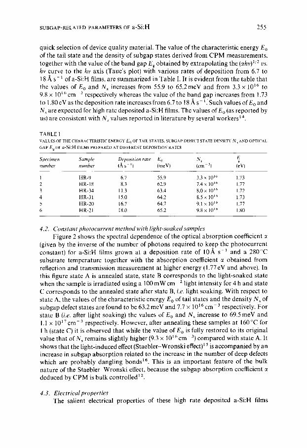
SUBGAP-RELATED PARAMETERS OF a-Si:H 255
quick selection of device quality material. The value of the characteristic energy E o of the tail state and the density of subgap states derived from CPM measurements, together with the value of the band gap Eg obtained by extrapolating the (cthv) ~/2 vs.
hv curve to the hv axis (Tauc's plot) with various rates of deposition from 6.7 to 18 ~, s - 1 of a-Si:H films, are summarized in Table I. It is evident from the table that the values of E 0 and N s increases from 55.9 to 65.2 meV and from 3.3 × 10¹⁶ to 9.8 × 1016 cm 3 respectively whereas the value of the band gap increases from 1.73 to 1.80 eV as the deposition rate increases from 6.7 to 18 ,~ s ~. Such values of E o and Ns are expected for high rate deposited a-Si:H films. The values of E o (as reported by us) are consistent with N~ values reported in literature by several workers 14.
TABLE 1 VALUES OF THE CHARACTERISTIC ENERGY E 0 OF TAIL STATES. SUBGAP DEFECT STATE DENSITY N s AND OPTICAL
GAP Eg OF a-Si:H FILMS PREPARED AT DIFFERENT DEPOSITION RATES
Specimen Sample Deposition rate E o N s E g
number number (/~ s 7) (meV) (cm- 3) (eV)
1 ttR-9 6.7 55.9 3.3 × 10¹⁶ 1.73 2 HR-18 8.3 62.9 7.4 × 10¹⁶ 1.77 3 HR-34 11.3 63.4 8.0 x 10 t6 1.72 4 ttR-31 15.0 64.2 8.5 x 10¹⁶ 1.73 5 HR-20 16.7 64.7 9.1 x 10¹⁶ 1.77 6 ttR-21 I8.0 65.2 9.8 x 10 TM 1.80
4.2. Constant photocurrent me thod with l ight-soaked samples
Figure 2 shows the spectral dependence of the optical absorption coefficient c¢ (given by the inverse of the number of photons required to keep the photocurrent constant) for a-Si:H films grown at a deposition rate of 10~, s 1 and a 280°C substrate temperature together with the absorption coefficient ~ obtained from reflection and transmission measurement at higher energy (1.77 eV and above). In this figure state A is annealed state, state B corresponds to the light-soaked state when the sample is irradiated using a 100mWcm 2 light intensity for 4h and state C corresponds to the annealed state after state B, i.e. light soaking. With respect to state A, the values of the characteristic energy Eo of tail states and the density N s of subgap defect states are found to be 63.2 meV and 7.7 x 1016 cm- 3 respectively. For state B (i.e. after light soaking) the values of E0 and Ns increase to 69.5 meV and 1.1 × 1017 cm-3 respectively. However, after annealing these samples at 160 °C for 1 h (state C) it is observed that while the value of E o is fully restored to its original value that of N, remains slightly higher (9.3 x 10¹⁶ c m 3 ) compared with state A. It shows that the light-induced effect (Staebler-Wronski effect) 1 s is accompanied by an increase in subgap absorption related to the increase in the number of deep defects which are probably dangling bonds ~6. This is an important feature of the bulk nature of the Staebler-Wronski effect, because the subgap absorption coefficient c~ deduced by CPM is bulk controlled 12
4.3. Electrical propert ies The salient electrical properties of these high rate deposited a-Si:H films

256 .,,. I Y A G I WI ~l/.
5 I 0 ,
4
<,.5 ~ i I
U,
@
z IC
C'
0 IC, ] 1 . • •
<7 4 J 8 I 2 6 2 O 2 4 EbiER(;'r" ( e V )
l i g . 2. S p e c l r a l d e p e n d e n c e e l o p t i c a l ab~ ,o rp th )n ~:ocllicient x g i v e n t~ ~ r t [~c i l lvorse o f the n u m b e f
o f p l l o t o n x requ i red to keep lhe p h o t o c t i r r c n l ccmstanl Ior a -S i :H IHnas grox~n tit tl d c p o s i l i o n ra ie i , f
I l l ,\ s i a! a 2}411 ( ' -,tlbStl-alt_' lcnlpcf{ l tLIrt. ' it1 (i} -;talc' ,,\ (a l l l l ca led s l a l e l l I, (t it Male' t'} [ l ight s o a k e d clsing
I l l ( i m W c m -' l ight i n t cns i l ) fo r 4 h l l , i and diii s la lc ( d i g h t - ~ o a k e d and annea led sta le l I~q. The <~pcctra] depei ' /dence o f ;, de te rm ined I ron/ r t . ' l lecl ion Hlld l i~ l l lSmission illc{isLirt_'lllL'rllS is cilso sho~3, n l i i ) .
deposited wi th rates vary ing from 6.7 A s ~ to l g A s ~ Iwhich have previously been reportcd I" in detail) arc as follows: (i) dtirk conduct ivi ty al 25 (', l0 11 10 9 i~ 1
cm 1 (it) phoioconduct iv i ty tit a 100roW cm e light n t ens ty , 1() ~ 10 4 t i cm 2. (iiil photosensit ivi ty rrph, cs,--- 3 × I(P 4 × 10⁵: (iv) exponent n of photocon- ductivitv, 0.76 0.84; (x,l densities of states derived from space-charge-limited current (SCLC) measurements in the samples deposited tit a rate of 6 g/~ s i are 5 × I0 ~ ~
g × 10 ~ 5 cm ;~ eV 1. It is known ~s that the values densities of states calculated from S( 'LC measurements made in thc n i n (sandwiched) cont igurat ion are in general Iov,,er than the values determined by CPM and photoihermal deflection spectros- copy techniques etc. The electrical properties of these high rate deposited a-Si:H lilms w,ith various rates from 6.7/~ s ~ to 18.0 ~ s ~ seem to be in agreement with the subgap absorpt ion parameters E~ and N~ reported ilere.
5. ( ' ( ) N ( ' l I:SII{IN
T h e C P M has been used to derive informat ion about the absorpt ion coefficient in the subgap region, the characteristic energy Eo of tail states and the density of subgap defect states of a-Si:H films deposited with various rates ranging from 6.7/~ s ' to 18 ~ s i. Between these extreme values of the deposit ion rates the value of E o is found to increase from 55.9 to 65.2meV, N~ from 3 . 3 x 1 0 l~' to 9.8× 10~"cm ~ and the bandgap E. fiom 1.73 to 1.80cV. The disorder seems to increase marginal ly with increasing rate of deposit ion of lilms (6.7 18.0/~s 1). Further. it has been found that the light soaking enhances the value of the

SUBGAP-RELATED PARAMETERS OF a-Si:H 257
characteristic energy E0 and defect density Ns in the material and this is accompanied by an increase in the subgap absorption related to an increase in the number of defects, probably dangling bonds. By and large the optoelectronic properties appear to be reasonably good up to a deposition rate of 18/~ s ~ and these films appear to be suitable for various applications requiring high growth rate such as electrophotographic drums.
ACKNOWLEDGMENTS
The authors are grateful to the Director, National Physical Laboratory, New Delhi, India, for giving permission to publish this paper and to the DNES, Government of India, for financial support. They acknowledge Dr. P. J. George, Kurukshetra University, for helpful discussions. Thanks are also due to the learned referees for pointing out certain drawbacks in the results reported in the original manuscript.
REFERENCES
1 R. Ranganathan , M. Gal and P. C. Taylor, Sol. Cells, 24 (1988) 257. 2 J. Kocka, M. Vanecek, J. Stuchlik, O. Stika, E. Sipek, H. T. Ha and A. Triska, in W. H. Bloss and G.
Grassi (eds.), Proe. 4th European Communities' Photovoltaic Solar Energy Conl:, Stresa, Reidel, Dordrecht, 1982, p. 443.
3 M. Vanecek, J, Kocka, J. Stuchlik, Z. Kozisek, O. Stika and A. Triska, Sol. Energy Mater., 8 (1983) 411.
4 H .G . Grimmeiss and L. A. kedebo, J. Appl. Phys., 46 (1975) 2155. 5 J .I . Pankove, Sol. Cells, 24 (1988) 299. 6 A. Tyagi, B. S. Satyanarayan, P. N. Dixit, T. Seth, A. Basu, R. Bhanacharyya and V. V. Shah, Proe.
Int. Cot~[i on Semiconductor Materials. New Delhi, December8 16, 1988. 7 R . S . Crandall, in J. I. Pankove (ed.), Semiconductors and Semimetals, Vol. 21B, Hydrogenated
Amorphous Silicon, Academic Press, New York, 1984, p. 245. 8 A. Madan and M. P. Shaw, in The Physics and Applications of Amorphous Semiconductors,
Academic Press, New York, 1988, p. 161. 9 M. Vanecek, J. Kocka, J. Stuchlik and A. Triska, Solid State Commun., 39 ( 1981 ) 1199.
10 N . M . Amer and W. B. Jackson, in J. I. Pankove (ed.), Semiconductors and Semimetals, Vol. 21 B, Hydrogenated Amorphous Silicon, Academic Press, New York, 1984, p. 83.
11 Z .E . Smith, V. Chu, K. Shepard, S. Aljishi, P. Stobodin, J. Kolodzey and S. Wagner, Appl. Phys. Lett.,50(1987) 1521.
12 J. Kocka, M, Vanecek and A. Triska, in H. Fritzsche (ed.), Amorphous Silicon and Related Materials, Vol. 1, World Scientific Publishers, London, 1989, p. 297.
13 J~ Kocka, M. Vanecek, Z. Kozisek, O. Stika and J. Beichler, J. Non-Cr.vst. Solids, 59-60 ( 19833 293. 14 Z .E . Smith, ~n K. Tanaka (ed.), Glow Discharge Hydrogenated Amorphous Silicon, K T K Scientific
Publishers, Tokyo, Kluwer Academic Publishers, London, 1989, p. 101. 15 D.L. Staebler and C. R. Wronski, Appl. Phys, Lett., 31 (19773 292; J. Appl. Phys., 51 (1980) 3262, 16 J. Kocka, M. Vanecek, J. Stuchlik, O. Stika, 1. Kubelik and A. Triska, in R. Grigorovici (ed.), Proc.
Int. Con/i on Amorphous Semiconductors. Bucharest, August September, 1982, p. 150. 17 T. Seth, P. N. Dixit, B. S. Satyanarayan, O. S. Panwar, A. Tyagi, R. Bhattacharyya and V. V. Shah,
20th hit. Cm![~ on Physies o['Semieonduetors. Thessaloniki, August 6 10. 1990. 18 J. 1. B. Wilson, in Properties of Amorphous Silicon, EM1S Datareviews Series No. 1, INSPEC,
London, 2nd edn., 1989, p. 131.