study of nonlinear behavior and chaos phenomena in power ... · been made to study the bifurcation...
TRANSCRIPT

International Journal of Engineering and Applied Sciences (IJEAS)
ISSN: 2394-3661, Volume-5, Issue-2, February 2018
59 www.ijeas.org
Abstract— A study has been done for chaos and bifurcation
phenomena in a various kind of single and three phase dc to ac
inverter along with nine level stepped wave inverter. The
converters are simulated using a software package
MATLAB/SIMULINK. It is observed that the inverters moves
from periodic operation state to chaotic operation state as
bifurcation parameter like input voltage frequency and load to
the inverter is changed. The bifurcation pathway includes
smooth period-doubling bifurcations as well as border collision
bifurcations. Simulated results output voltage and current
waveform of single and three phase inverter along with stepped
wave inverter are validated by waveforms and FFT
spectrum. .Inverters with a large number of steps can generate
high quality voltage waveforms. The simulation of single phase
three level, three phase h-bridge inverter and nine stepped wave
inverters is done in software Matlab/Simulink. The FFT
spectrums for the outputs are compared and presented to
validate the proposed control strategy. This information leads a
powerful role for designing practical circuits in power
electronics.
Index Terms— Bifurcation, dc-ac inverter, Chaos, Stepped
wave inverter
I. INTRODUCTION
All types of power electronics converters may be classified
as on linear time-varying dynamical systems because they
exhibit a wealth of nonlinear phenomena, including various
kinds of bifurcations and chaos. The principal source of
non-linearity is the inherent switching action and presence of
a potential source of engineering malfunction and failure. In
order to avoid these phenomena it is very important to predict
and analyze these nonlinear phenomena of a converter.
nonlinear components (e.g. the power diodes) and control
methods (e.g. pulse-width modulation). These nonlinearities
are the occurrence of bifurcations and chaos in power
electronics was first reported in the literature by Hamill [1] in
1988. Experimental observations regarding bounded ness,
chattering and chaos were also made by Krein and Bass [2]
back in 1990. Although these early reports did not contain any
rigorous analysis, they provided solid evidence of the
importance of studying the complex behavior of power
electronics and its possible benefits for practical design.
Using an implicit iterative map, the occurrence of
period-doublings, sub-harmonics and chaos in a simple buck
converter was demonstrated by Hamill [3] using numerical
analysis, PSPICE simulation and laboratory measurements.
Sanjeev Kumar, Electrical and Electronics, S.R.M.S.College of Engg. &
Technology, Bareilly, India, 9458702654.
Dr.G.K.Banerjee, Electrical Engg.Department, IFTM University,
Moradabad, India, 9557350400
Dr.Piush Kumar, Electrical and Electronics, S.R.M.S.College of Engg.
& Technology, Bareilly, India, 9458702505,
Rajesh Kumar, Electrical and Electronics, MBM Engineering College
Jodhpur, India, 9458701261
The derivation of a closed-form iterative map for the boost
converter under a current-mode control scheme was presented
later by the same group of researchers [4, 5].Further work on
the bifurcation behavior of the buck converter was
investigated by Chakrabarty [6] who specifically studied the
bifurcation behavior under variation of a range of circuit
parameters including storage inductance, load resistance,
output capacitance, etc. In 1996,Fossas and Olivar [7]
presented a detailed analytical description of the buck
converter dynamics, identifying the topology of its chaotic
attractor and studying the regions associated with different
system evolutions.
Power electronics is a relatively new and fast-growing area of
electronics with wide practical application. In particular, the
stability and the bifurcation analysis of the power electronics
systems with the pulse-width modulation (ab. PWM)
technique has attracted much interest in recent years [8], [9].
Over the past years, a new type of bifurcation phenomena
called border-collision bifurcation has been discovered for
one or two-dimensional one-parameter families in discrete
systems [10], [11].
In reality, bifurcation is to be avoided, but it is also known that
designing a system too remote from bifurcation boundaries
may degrade performance characteristics. Hence, efforts have
been made to study the bifurcation behavior in single, three
and nine stepped wave inverters, to show the practical
relevance of bifurcations and chaos in power electronics
systems. In the first stage simulation are carried out for the
single and three phase H-bridge converters, to investigate
nonlinearities. In order to provide stable operation for
conversion dc in to ac. Input dc can be obtained from battery,
fuel cell, Chopper, solar cell etc.
In second stage, the nine stepped inverter is achieved by
cascading four single phase H-bridge inverter. This stepped
wave inverter has fixed input voltage and a variable output ac
voltage as number of H-bridge inverter increase or decrease.
The inverters are simulated through a powerful software
package MATLAB/SIMULINK. Voltage current waveforms
and FFT spectrum are obtained with change in input
parameter values to obtain nonlinearities and complex
behavior.
II. BASIC PRINCIPLE
A single phase three stage H-bridge inverter is shown in Fig.
1. The inverter in first stage provides the three state output as
well as converts pure dc in to ac .It consist of four Power
semiconductor devices which operates as
switches(T1,T2,T3,T4), to the output voltage of desired
magnitude and frequency. At the same time only two switches
Study of Nonlinear Behavior and Chaos Phenomena
in Power Inverter
Sanjeev Kumar, Dr. G.K Banerjee, Dr.Piush Kumar, Rajesh Kumar
Study of Nonlinear Behavior and Chaos Phenomena in Power Inverter
60 www.ijeas.org
operates and remaining two switches are in off stage. This
circuit is easily realized by four switches, a voltage source, an
inductor and a resistor. The four switches are named by T1,
T2, T3, and T4. This circuit has the following two conditions.
State A: T1 and T3: ON
T2 and T4: OFF,
State B: T1 and T3: OFF
T2 and T4: ON,
Table I: Switching States Single Phase Inverter
T1 T2 T3 T4 VA VB
ON OFF ON OFF
_
OFF ON OFF ON + +
ON OFF ON OFF
_
OFF ON OFF
ON
+
+
Fig. 1: Simulink model of Single phase H-Bridge
inverter
H Bridge DC-AC converter operating waveforms is shown in
Fig. 5. In one switching cycle, the arriving of clock pulse drives
T1 and T3 on, T2 and T4 off, the inductor current increases;
when the inductor current reaches the compensated current
reference˜iref, T1 and T3 off, T2, T4 on, the inductor current
begins to decline.
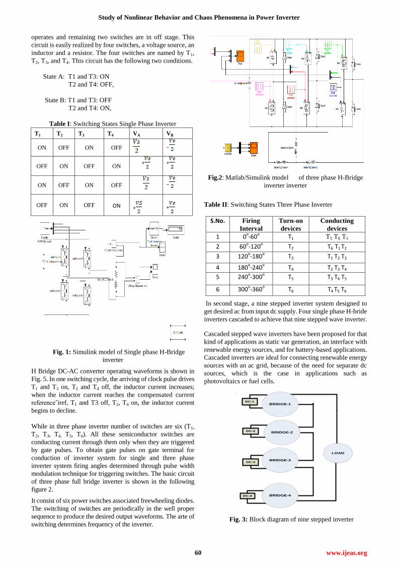
While in three phase inverter number of switches are six (T1,
T2, T3, T4, T5, T6). All these semiconductor switches are
conducting current through them only when they are triggered
by gate pulses. To obtain gate pulses on gate terminal for
conduction of inverter system for single and three phase
inverter system firing angles determined through pulse width
modulation technique for triggering switches. The basic circuit
of three phase full bridge inverter is shown in the following
figure 2.
It consist of six power switches associated freewheeling diodes.
The switching of switches are periodically in the well proper
sequence to produce the desired output waveforms. The arte of
switching determines frequency of the inverter.
Fig.2: Matlab/Simulink model of three phase H-Bridge
inverter inverter
Table II: Switching States Three Phase Inverter
S.No. Firing
Interval Turn-on
devices Conducting
devices
1 0o-60
o T1 T5 T6 T1
2 60o-120
o T2 T6 T1 T2
3 120o-180
o T3 T1 T2 T3
4 180o-240
o T4 T2 T3 T4
5 240o-300
o T5 T3 T4 T5
6 300o-360
o T6 T4 T5 T6
In second stage, a nine stepped inverter system designed to
get desired ac from input dc supply. Four single phase H-bride
inverters cascaded to achieve that nine stepped wave inverter.
Cascaded stepped wave inverters have been proposed for that
kind of applications as static var generation, an interface with
renewable energy sources, and for battery-based applications.
Cascaded inverters are ideal for connecting renewable energy
sources with an ac grid, because of the need for separate dc
sources, which is the case in applications such as
photovoltaics or fuel cells.
DC-1
DC-3
DC-2
DC-4
BRIDGE-1
BRIDGE-2
BRIDGE-3
BRIDGE-4
LOAD
Fig. 3: Block diagram of nine stepped inverter

International Journal of Engineering and Applied Sciences (IJEAS)
ISSN: 2394-3661, Volume-5, Issue-2, February 2018
61 www.ijeas.org
From the single phase structure of a cascaded H-bridge
inverter as shown in Fig. 1 above, we can make the three level,
five level, seven level, nine level, and eleven level inverters
without using any type of modulation technique, and by this
topology, the number of output-phase voltage steps is defined
by P= 2Q+1, where ‘’ is the no of levels and ‘Q’ is the
number of DC sources. So, for an example the output phase
voltage of nine stepped wave inverter is given by
Van= Va1+Va2+Va3+Va4 (1)
Where Va1, Va2, Va3, Va4 are the voltages across output
terminals of h-bridge inverters of nine stepped inverter.
Van= Va1+Va2+Va3 (2)
This output voltage is valid for seven stepped inverter which
require three h-bridge inverter.Simelarly output voltage of
different stepped inverter can be obtain.
Under the assumption that the inductor current is
essentially piecewise linear, the dynamics of the controlled
current is described by the following map:
In+1 = In + m1T if In ≤ Iref - m1T (3)
In+1 = Iref –m2tn
if In> Iref - m1T (4)
Where In = IL (nT) is the value of the inductor current at the
clock instant nT; m1 and m 2 are respectively the magnitudes of
the slopes on the increasing and decreasing segment of IL and tn
is the duration of the OFF cycle in the clock in the cycle
between nT and nT + T. Under steady state operation in
periodic or chaotic mode, with a constant input voltage V in and
a low ripple output voltage of constant average value Vout, the
constants m1, m2 and can be expressed as:
m1 = (Vin –Vout) / L
& m2 = Vout/L (5)
(3)
= (m2 /m1)
= Vout / (Vin-Vout) (6)
Here is the ratio of slopes magnitude. If > 1 then, state of
operation of the inverter is unstable and circuit has no stable
periodic solution. Fig. 2 shows a typical segment of the
inductor current, I L , o f a dc-ac converter under current mode
control in the chaotic regime.
Iref
nT (n+1)T (n+2)T
t*nIL
t
m2m1
Fig. 4: Typical segment of inductor current for chaotic
regime, >1
Fig.5: Bifurcation diagram
III. SIMULATION RESULTS
All inverter circuits of Fig.1,Fig.2 and Fig.12 are simulated
on the powerful software package MATLAB/SIMULINK
Fig. 5 shows the Output voltage waveform of single phase
h-bridge inverter (period one operation) with input voltage
100V and R=10,L=10mh,Modulation Index=0.44,
frequency=50Hz . Figure.6 shows enlarge view of output
voltage and current waveform when Vin=100V, R=10Ω,
L=10mh, modulation Index=0.8, frequency=50Hz which
gives stable period-1 operation and first orbit comes into
existence. Hence the converter operates in period one
operation. Unstable states of voltage and current waveforms
When input voltage=300V,R=100Ω,L=60mh,
modulation index=0.8, frequency=50Hz indicated in Fig. 7 &
Fig.8.Therefore this orbit subsequently undergoes a
border-collision, and around that point another coexisting
higher period orbit comes into existence. Top most waveform
shows the output current waveform, which reaches in to
chaotic state value. Hence the inverter moves to operates in
period one operation to chaotic mode operation as bifurcation
parameter changes.
Fig. 5: Output voltage waveform of single phase inverter
(period one operation)
Fig.6: Enlarge view of output voltage and current waveform

Study of Nonlinear Behavior and Chaos Phenomena in Power Inverter
62 www.ijeas.org
Fig.7: output voltage and current waveform
Fig 8: Enlarge view of output voltage and current waveform
in unstable state
Fig. 9: Output Voltage Waveform of Power Bridge Inverter
Fig. 10: Distorted load current after variation in Load
Fig. 11: Voltage waveform of Three Phase Inverter
Fig. 11 shows the voltage waveform of Three Phase Inverter
when input voltage ,Vin=100volt , R=100 Ω,,L=15mh, ,
modulation index=035 frequency being 200Hz. the inverter
operates in period one operation at this stage.Fig.12 and Fig.13
gives voltage waveform of Three phase Power H-Bridge
inverter in unstable mode on input supply Vin=200V,
R-=100Ω, ,L=10mh , modulation index=0.75 ,carrier
frequency=200Hz as the bifurcation parameter is varied. The
same bifurcation structure is obtained when the bifurcation
parameter are changed to original value. Fig. 15 Enlarge view
of output voltage waveform in chaotic mode that shows
inverter enter stable operation to unstable operating state.
Fig. 12: Distorted voltage waveform of Three Phase Power
H-Bridge Inverter
Fig. 13: Enlarge view of voltage waveform of Three Phase
Power H-Bridge Inverter in unstable mode
Fig. 14: Voltage waveform of Three Phase Power H-Bridge
Inverter ln chaotic mode
Fig. 7 shows an enlarged view of the Inductor current
waveform when input voltage is 45V. Inductor current shows
irregular pattern. It is bounded by maximum reference value
and missed some clock pulses. Inductor current states do not
repeat at the clock instant. Hence converter operates in
chaotic mode
Fig. 15: Enlarge view of output voltage waveform in chaotic
mode

International Journal of Engineering and Applied Sciences (IJEAS)
ISSN: 2394-3661, Volume-5, Issue-2, February 2018
63 www.ijeas.org
IV. CASCADED NINE STEPPED INVERTER
The new development in the field of power electronics and
microelectronics made it possible to reduce the magnitude of
harmonics with multilevel inverters, in which the number of
levels of the inverters are increased rather than increasing the
size of the filters. The performance of multilevel inverters
enhances as the number of levels of the inverter increases.
The AC outputs of various full h-bridge inverters are connected
in series such that the synthesized voltage waveform is the sum
of the individual converter outputs.
Fig. 16: Simulink model of nine stepped wave inverter
Fig. 17: Internal circuit for subsystem of nine stepped wave
inverter
V. SIMULATION RESULTS OF STEPPED INVERTER
Simulation results are obtained by observing voltage and
current waveforms at variable load and input supply voltage
(Vin.) as bifurcation parameter. When the input supply voltage
Vin varies from higher voltage to lower voltage, there is change
in the dynamics.Fig.18 demonstrates the output voltage
waveform V2 recorded and current through when supply
voltage waveform Vin was 3 volts and load have only R=10 Ω,
only. This waveform is periodic (period-1 operation). In Fig.20
shows the output voltage and current waveform in unstable
state when R=10 Ω, L=10mH and input supply voltage Vin
=3V. Fig.22 to Fig 25 shows output voltage and current
waveform in unstable state of nine stepped for the
corresponding chaotic or strange attractor (graph between
output voltage and current) has been drawn.
Inverter has transitioned by means of period doubling from
periodic to chaotic operation. In short, power electronic circuits
can exhibit nonlinear dynamics for example bifurcations, sub
harmonic oscillations and chaos.
It is observed that the inductor current waveform during the
switch on and switch off of the switch has “ringing” (fast
damped oscillations) due to the presence of parasitic
Fig. 18: Enlarge view of output voltage and current waveform
in stable state (period-1)
Fig. 19: FFT spectrum of nine stepped inverter for voltage
(Vin = 3V, R=10Ω)
Fig. 20: Distorted output voltage and current waveform in
unstable state

Study of Nonlinear Behavior and Chaos Phenomena in Power Inverter
64 www.ijeas.org
Fig. 21: FFT spectrum for voltage of nine stepped inverter
for o/p voltage (Vin = 3V, R=10Ω, L=10mH)
Fig. 22: Enlarge view of output current in period two
operation
Fig. 23: output voltage and current waveform in unstable
state
Fig. 24: Output voltage and current waveform in unstable
state
Fig. 25: Enlarge view of output voltage and current waveform
in chaotic state
Fig. 26: FFT spectrum of nine stepped inverter for current
VI. CONCLUSION
Bifurcation phenomena and nonlinear behavior investigated
in the various types of dc to ac converter such as single, three
and nine stepped wave dc to ac power converter. The inverter
shows peculiar behavior as the bifurcation parameter like
input voltage, to the inverter and nature of load is changed.
Current, voltage waveforms and fast Fourier transform
spectrum are obtained against various values of R,R-L load,
which show that how inverters operates in period one, period
two, higher periods and chaotic mode. The bifurcation
pathway includes smooth period-doubling bifurcations as
well as border collision bifurcations. Different values of the
input voltage, load the orbit undergoes a bifurcation, and the
system subsequently obtain to chaotic condition.
REFERENCES
[1] D.C. Hamill and D.J. Jefferies, "Sub-harmonics and chaos in a controlled
switched-mode power converter," IEEE Trans. Circ. Syst. I, vol. 35, pp
1059-1061 (1988)
[2] P.T. Krein and R.M. Bass, "Types of instabilities encountered in simple
power electronics circuits: unbounded ness, chattering and chaos,"
IEEE Applied Power Electron. Conf. Exp., pp. 191-194, 1990.
[3] J.H.B. Deane and D.C. Hamill, “Analysis, simulation and experimental
study of chaos in the buck converter”, Power Electronics Specialists
Conference Record, vol. II, pp 491-498 (1990)
[4] J.H.B. Deane and D.C. Hamill, “Chaotic behavior in a current-mode
controlled DC-DC converter”, Electronics Letters, vol. 27, no. 13, pp
1172-1173 (1991)
[5] J.H.B. Deane, “Chaos in a current-mode controlled boost dc-dc
converter”, IEEE Transactions on Circuits and Systems, vol. 39 no. 8,
pp 680-683 (August 1992)
[6] K. Chakrabarty, G. Podder and S. Banerjee, "Bifurcation behaviour of
buck converter," IEEE Trans. Power Electron., vol. 11, pp. 439-447,
1995
[7] E. Fossas and G. Olivar, "Study of chaos in the buck converter," IEEE
Trans. Circuit &. System, I, vol. 43, pp. 13-25, 1996.
[8] S. Banerjee, G. C. Verghese ed., “Nonlinear Phenomena in Power
Electronics: Attractors, Bifurcations, Chaos, and Nonlinear Control,”
Wiley-IEEE Press, 2001.
[9] M. di Bernardo, C. K. Tse, “Chaos in Power Electronics: An
overview,”Chaos in Circuits and Systems, chapter 16. World
Scientific, pp. 317–340, 2002.
[10] H. E. Nusse and J. A. Yorke, “Border-Collision bifurcations
including‘period two to period three’ for piecewise smooth systems,”
Physica, D57, pp. 39–157, 1992.
[11] H. E.Nusse and J. A. Yorke, “Border-Collision Bifurcations For
Piecewise Smooth One-Dimensional Maps,” International Journal of
Bifurcation and Chaos, vol. 5-1, pp. 189-207, 1994.
.

International Journal of Engineering and Applied Sciences (IJEAS)
ISSN: 2394-3661, Volume-5, Issue-2, February 2018
65 www.ijeas.org
AUTHORS PROFILE
Sanjeev Kumar graduated from Shri Ram Murti
College of Engineering and Technology, Bareilly India, in 2001, and
received his Master’s degree in 2006,from the MNNIT ALLAHABA He is
currently working as Assistant Professor in Department of Electrical and
Electronics Engineering SRMSCET, Bareilly, He is currently pursuing his
Ph.D. from the IFTM University, Moradabad .He is life time member of
institute of engineers. His research interests include application His main
research work focuses on Chaos and bifurcation, dc to dc converter, dc to ac
converter and power converters, complex behavior of power electronics
systems. He has 17 years of teaching experience. He has several publications
in Journals and Conferences in his field. He has attended National
Conferences and presented papers there.
Dr.G.K.Banerjee PhD, is currently Professor and Head,
Department of School of Engineering and Technology (SET), Institute of
Foreign Trade and Management (IFTM) University, Moradabad. He has
been former Professor in the Department of Electrical Engineering, College
of Technology, G.B. Pant University of Agriculture and Technology,
Pantnagar, Uttara hand. Dr. Banerjee has been teaching and conducting
research work since last 34 years. He is a member of ISTE and
Semi-conductor Society (India).
Dr.Piush Kumar graduated from Karnataka
University Dharwad, in Electrical and Electronics Engineering in 1998 and
received his Master’s degree in 2003, from M.M.M. Engineering College,
Gorakhpur. He did his Ph.D. from MNNIT, Allahabad, India. At present, he
is Associate Professor in the Department of Electrical Engineering at Shri
Ram Murti College of Engineering and Technology, Bareilly. He is life time
member of institute of He has several publications in Journals and
Conferences in his field. He has attended National Conferences and
presented papers there.
Rajesh Kumar received his B.Tech. And M.E. degrees
in Electrical Engineering from RTU, Kota and JNVU Jodhpur respectively.
He is currently pursuing his Ph.D. from the MBM Engineering College
Jodhpur. His research interests include distribution and transmission power
systems, optimization, and system theory, smart grid and wide area control
system.