study of space condition effect and analyzing digital
TRANSCRIPT
1
MASTER THESIS
Study of space condition effects and analyzing digital
techniques for improving RF power amplifier's linearity
and efficiency for small satellites
Kamran Haleem
SUPERVISED BY
Pere L. Gilabert Pinal
Gabriel Montoro Lopez
Universitat Politècnica de Catalunya
Master in Aerospace Science & Technology
Sept 2015

2
This Page Intentionally Left Blank

3
Acknowledgments
Firstly, I am much grateful to God for providing the good health and wellbeing that was
necessary for completing this master thesis.
I would like to express my deepest appreciation and gratitude to my advisor Prof. Pere
L. Gilabert Pinal for the continuous support and help provided by him during entire
thesis related research. His motivation and guidance abetted me to complete my
research and his insightful comments has made this dissertation presentable.
Besides my advisor, I would like to thanks my co-advisor Prof. Gabriel Montoro Lopez,
whose prompt availability and precious support has assisted me in several occasion.
My sincere thanks also goes my colleague Teng Wang for providing knowledge on the
basics of his work (related to my research) as well as guidance in various instances.
Furthermore, I am much thankful to Chalmers University of Technology, Sweden for
allowing me to remotely access the Web Lab setup for the real-time hardware
implementation and testing of my designed algorithms.
Last but not the least, I would like to express sincere thanks and regards to my family
and friends whose spiritual support was along with me throughout my master’s degree
and my life in general.

4
This Page Intentionally Left Blank

5
Abstract:
Objective of modern small satellite communication is to provide the end users with
higher data rate downlink capability, in addition to, reliability and system efficiency. A
significant device, with respect to power consumption and influence on system
linearity, use in the transmission chain of small satellites, is power amplifier. The power
amplifier tends to add distortion and non-linearity in the transmitted signal, when
operating close to saturation point. For avoiding the non-linearity addition by the PA, it
should be operated in linear region which causes the degradation in power efficiency.
Therefore, for having the maximum power efficiency and improving linearity, the
predistortion should be performed before inputting the signal to power amplifier. For
compensating non-linear distortion, linearization scheme based on digital predistortion
is used, which requires a feedback path for adaptation and extraction of new
coefficients for DPD. Hence for making the DPD adaptive, ADC is required to add in
the system. As a consequence of performing digital predistortion, the spectral regrowth
occurs which causes the increase in bandwidth up to five times of original signal. Due
to this reason, digital to analog converter has to sample the signal at five times of
nyquist frequency which increases the cost and power consumption of DAC.
This master thesis presents the methodology implementation for compensating the
non-linear distortion in PAs, applicable for small satellite communication, with a
cooperative technique of digital and analog predistortion. This thesis provides with the
solution for the increased sampling rate of signal at analog to digital converter with a
use of combination of digital and analog predistortion. The predistortion (digital and
analog) is design to focus on maximizing the linearity and minimizing the distortion and
spectral regrowth. While the adaptive scheme of combined digital predistortion and
analog predistortion (simulated) is designed, with an ideal low-pass filter between
them, for implementation ease of the digital-to-analog converter and decrease in signal
sampling rate.
The results provided in the thesis have shown that same linearity and efficiency can
be achieved at amplifier’s output by implementing the above mentioned solution with
a benefit of reducing the signal sampling frequency at DAC. A comparative analysis of
power amplifier behavior in various configuration is presented in the dissertation.

6
This Page Intentionally Left Blank

Contents
Acknowledgments .................................................................................... 3
Abstract: .................................................................................................... 5
Glossary .................................................................................................. 13
Chapter 01 ............................................................................................... 15
1.1. Introduction: .................................................................................... 15
1.2. Background and Motivation: ............................................................ 15
1.3. Thesis Outline ................................................................................. 16
Chapter 02 ............................................................................................... 18
2.1. Satellite communication – Transmitter............................................. 18
2.2. Power Budget: ................................................................................ 19
2.3. Power Amplifiers – Description and Comparison: ............................ 20
2.4. Modulation Scheme Comparison: ................................................... 22
2.5. Doppler Effect for LEO satellites: .................................................... 25
Chapter 03 ............................................................................................... 28
3.1. Power Amplifier linearization techniques ......................................... 28
3.2. Methods to compensate Non-linearity in PA behavior ..................... 29
3.2.1. Feed Back system: ....................................................................................... 29
3.2.2. Feed forward System: ................................................................................... 30
3.2.3. Predistortion: ................................................................................................. 31
3.2.3.1 Predistortion System Configurations: ................................................................................. 33
3.2.3.2 Memory/Memoryless Effect: .............................................................................................. 33
3.2.3.3 Static/Adaptive Predistortion System: ................................................................................ 35
Chapter 04 ............................................................................................... 38
4.1. Implementation of Adaptive DPD Algorithm .................................... 38
4.2. Design and Implementation Procedure: .......................................... 38
4.3. PA Behavioral Modelling: ................................................................ 39
4.4. Predistortion: ................................................................................... 43

8
4.5. Static DPD Assembly: ..................................................................... 45
Chapter 05 ............................................................................................... 47
5.1. Web Lab setup for PA Predistortion implementation ....................... 47
5.2. Adaptive Predistortion Implementation through Web Lab ................ 48
Chapter 06 ............................................................................................... 56
6.1. Cascaded PD Implementation ......................................................... 56
6.2. Emulated APD design: .................................................................... 56
6.3. Low-pass Filter Designing: .............................................................. 57
6.4 Adaptive DPD and APD Model: ........................................................ 58
Chapter 07 ............................................................................................... 65
7.1. Conclusion ...................................................................................... 65
Bibliography ............................................................................................ 68

9
Table of Figures
Figure 1: Transmitter chain assembly ........................................................................... 18
Figure 2: Frequency vs output power ............................................................................ 20
Figure 3: Input power vs output power .......................................................................... 20
Figure 4: Comparison in terms of Output power, input power and PAE [2] ................... 21
Figure 5: Input power vs phase shift [2] ......................................................................... 21
Figure 6: Transmitted constellation at PA output ........................................................... 22
Figure 7: Transmitted constellation before amplification ............................................... 22
Figure 8: Modulation schemes in terms of power consumption vs data rate ................. 23
Figure 9: 16 QAM performance in presence of non-linear amplifier with or without
predistortion .................................................................................................................. 24
Figure 10: Modulation Schemes comparison in terms of Average SNR vs Capacity .... 25
Figure 11: Doppler Frequency Shift Curve .................................................................... 26
Figure 12: Doppler Rate Curve ..................................................................................... 26
Figure 13: Local Feedback System ............................................................................... 29
Figure 14: Global Feedback System ............................................................................. 30
Figure 15: Baseband Feedback System [12] ................................................................ 30
Figure 16: Feed Forward Linearization System ............................................................. 31
Figure 17: Predistortion before Modulation ................................................................... 31
Figure 18: Predistortion after Modulation ...................................................................... 31
Figure 19: Closed Loop Predistortion [12] ..................................................................... 32
Figure 20: Predistortion System .................................................................................... 32
Figure 21: Memoryless Vs Memory polynomial Analysis Diagram ................................ 34
Figure 22: Static Predistorter ......................................................................................... 36
Figure 23: Static Predistorter with LUT [23] ................................................................... 36
Figure 24: Adaptive predistortion system [24]. .............................................................. 36
Figure 25: Adaptive predistortion algorithm block diagram ............................................ 37
Figure 26: Flow diagram of DPD implementation phase ............................................... 38
Figure 27: PA input and output power spectrum without linearization technique .......... 42
Figure 28: AM/AM curve for memoryless model of PA (Polynomial degree P=9) ......... 42
Figure 29: AM/AM curve for PA model with memory (a) Polynomial degree P=9,
Memory length M=6 (b) Polynomial degree P=9, Memory length M=15 ....................... 43
Figure 30: Implementation of PA Modelling ................................................................... 44
Figure 31: AM/AM curve, Memoryless DPD with polynomial degree P=9 ..................... 44
Figure 32: AM/AM curve for memory DPD for configuration (a) P=9, M=6 (b) P=9, M=15
...................................................................................................................................... 45
Figure 33: Static DPD Assembly .................................................................................. 45
Figure 34: Power Spectrum comparison at PA output (with and without DPD Assembly)
...................................................................................................................................... 46

10
Figure 35: AM/AM curve of static DPD assembly for configuration (a) P=9, M=0 (b) P=9,
M =6 .............................................................................................................................. 46
Figure 36: Web Lab Instruments [28] ............................................................................ 47
Figure 37: Adaptive DPD Block Diagram ...................................................................... 48
Figure 38: AM/AM curves, Memoryless Adaptive DPD (Polynomial degree P=9) ......... 50
Figure 39: Memoryless DPD (input and output) power spectrum .................................. 50
Figure 40: PA (input and output) power spectrum for memoryless adaptive DPD
assembly ....................................................................................................................... 51
Figure 41: AM/AM curves, Memory DPD configuration (Polynomial Degree P=9,
Memory length M=6) ..................................................................................................... 52
Figure 42: Input and output power spectrum of memory DPD configuration (Polynomial
degree P=9, Memory length M=6) ................................................................................. 52
Figure 43: PA input and output power spectrum with and without DPD ........................ 53
Figure 44: Memory DPD (P=9, M=6) input and output power spectral density estimate 53
Figure 45: PA input and output power spectral density estimate with and without DPD 54
Figure 46: AM/AM curve for Memory DPD and PA behavioral model with Polynomial
degree P=9, Memory length M=15 ................................................................................ 54
Figure 47: AM/AM curve of adaptive DPD assembly with Polynomial degree P=9,
Memory length M=16 .................................................................................................... 55
Figure 48: PA input and output power spectrum with memory DPD configuration
(polynomial degree P=9, Memory length=15) ............................................................... 55
Figure 49: Input and output spectrum (after fft) of ideal low-pass filter in logarithmic
scale .............................................................................................................................. 57
Figure 50: Input and output spectrum (after fft) of ideal low-pass filter in linear scale ... 58
Figure 51: Adaptive DPD + APD block diagram ............................................................ 58
Figure 52: DPD input and output (after fft) spectrum in logarithmic scale ..................... 59
Figure 53: Low-pass filter input and output (after fft) spectrum in logarithmic scale ...... 59
Figure 54: APD input and output (after fft) spectrum in logarithmic scale...................... 60
Figure 55: PA input and output (after fft) spectrum in logarithmic scale ........................ 60
Figure 56: DPD input and output PSD spectra in DPD+APD configuration ................... 61
Figure 57: DPD input and output power spectral density comparison without APD ...... 61
Figure 58: PA input and output power comparison with and without linearization
technique application..................................................................................................... 62
Figure 59: PA output PSD comparison with and without linearization technique
application ..................................................................................................................... 62
Figure 60: PA output spectrum (without DPD, with APD and With DPD+APD) ............. 63

11
List of Tables:
Table 1: Satellite Mass and Power ............................................................................................................. 19
Table 2: Properties comparison of different types of Amplifiers ................................................... 21
Table 3: Spectral efficiency for modulation methods ......................................................................... 23
Table 4: NMSE comparison ........................................................................................................................... 43
Table 5: Memory length effects on important parameters .............................................................. 54
Table 6: Polynomial degree effects on various parameters ........................................................... 57
Table 7: Final Results for various configurations ........................................................... 64

12
This Page Intentionally Left Blank
13
Glossary
ADC Analog-to-Digital Converter
AM Amplitude Modulation
APD Analog Predistorter
ACEPR Adjacent Channel Error Power Ratio
ACLR Adjacent Channel Leakage Ratio
ACPR Adjacent Channel Power Ratio
DPD Digital Predistortion
DAC Digital-to-Analog Converter
DDR Dynamic Deviation Reduction
HEMT High Electron Mobility Transistor
I/Q In-phase/Quadrature
LS Least-Squares
LMS Least Mean Squares
NMSE Normalized Mean Square Error
PA Power Amplifier
PAE Power Added Efficiency
PSD Power Spectral Density
QAM Quadrature Amplitude Modulation
RLS Recursive Least Square
SNR Signal-to-Noise Ration

14
This Page Intentionally Left Blank

15
Chapter 01
1.1. Introduction:
This Master Thesis addresses the study and implementation of cooperative digital and
analog predistortion technique for improving power amplifier’s linearity. It also caters the
solution for decrease in sampling frequency rate of digital to analog converter, that
occurred due to the bandwidth expansion around five times of original signal, caused due
to predistortion. The technique is implemented through simulating the model of power
amplifier in Matlab Software and then perform the analysis of result achieved through
feeding it to the predesigned real-time hardware test bed. The idea of this master thesis
involves the designing of adaptive predistortion system for that purpose the accurate
modelling of power amplifier is the initial and foremost step. Keeping in view of countering
memory effects and better modelling of power amplifier the Dynamic Deviation Reduction
Volterra Series is selected.
1.2. Background and Motivation:
In this era of communication, every communication technique has its significance and
effects on daily life of people. Satellite communication is currently a vast field of research
and improvement, whereas, substantial progress has been made in this regard recently.
With the advancement in this area, commercial large satellites are now being replaced
with the small (micro, nano and pico) satellites. These are largely using for the purpose
of communication, building constellations of satellites for certain objectives and in-orbit
inspection. Having certain advantages for this development, there are also few problems
in their implementation which needs to be countered. Due to the decrease in size, the on-
board power generation and storing capabilities have reduced by large factor. Therefore,
the power consumption of each instrument becomes comparatively more significant.
Power amplifier is one of high power consuming devices in the transmission chain of a
satellite. It not only consumes more power but also tends to add non-linearities which
effect the efficiency of system.
With the increase in demand of enhanced spectral efficiency and less distortion,
consequently affecting the power consumption, the multi-level modulation schemes were
introduced in past such as QAM (Quadrature Amplitude Modulation). These modulation
schemes are more sensitive to the non-linearity introduce by the power amplifier,

16
therefore, this matter has to be dealt with for making the transmission system more
efficient.
One of the trivial solution for this problem is the use of power amplifier in its linear region.
In this region of operation the average output power would be much less than the
amplifier’s saturation region output power. The drawback for this solution is that it will
make the transmission system costly and inefficient because of the fact that more power
will consumed while integrating more number of amplifier stages to achieve the required
gain and the power consumption is a major issue when the topic under consideration is
satellite communication (especially small satellites).
The other solution which is more complicated in terms of implementation but, on the other
hand, provides more linearity in PA behavior and reduce distortion. It comprises of
predistortion of the input signal so that it can counter the effects of non-linearities
introduce by power amplifier.
The predistortion technique is the development of inverse model of power amplifier
behavior. The inverse behavior of PA is introduced in the original signal before inputting
it to the power amplifier in a way that the output becomes linear. This methodology has
an effect on the bandwidth expansion of the signal, consequently, the digital to analog
converter has to be designed at the sampling frequency of up to five times of original
signal.
This master thesis represents the implementation of predistortion scheme for linearizing
the power amplifier’s behavior. It also provides the solution for decreasing the sampling
frequency of digital to analog converter up to, approximately, the same bandwidth as
original signal.
1.3. Thesis Outline
This master thesis is composed of three phases. First phase includes the literature review
and the study of few aspects which are quite important while designing a communication
system. Some of these parameters are the power budget (especially for the small
satellites), type and class of power amplifier and modulation scheme. A comparison is
provided regarding the selection of these parameters based on the research performed
in past. Another important issue in the communication is Doppler Effect which needs to
be countered. A brief explanation is compiled in one of the sections of this phase.
Second phase of this thesis majorly contributes towards the behavioral modelling of RF
power amplifier. Literature review has been provided regarding the selected model of PA
i.e. Volterra series. The implementation/simulation of the model has been done in Matlab.
With the use of modeled power amplifier, a static predistortion system has designed and
simulated. This phase of report also shows the results achieved on every step of
implementation and analysis/commenting is done with respect to the change in important

17
parameters. Furthermore, it consists of the concluding results of adaptive digital
predistortion with the use of hardware implemented power real-time power amplifier. For
this purpose, Web Lab is utilized to observe the behavior of designed system
In the third phase of this master thesis, a simulated APD (Analog predistorter) which is
essentially equivalent to a memoryless DPD is used in cascade with adaptive DPD
system designed previously by applying a low-pass filter between them for countering the
in-band distortions. The objective of this combination scheme is to reduce the bandwidth
expansion (caused by DPD) so that the sampling frequency of digital to analog converter
can be reduced for the ease of implementation. The analysis is provided on the factors of
normalized mean square error (NMSE), adjacent channel leakage ratio (ACLR) and
output power for proving the mentioned concept.
Finally, the conclusion and future work extension is projected at the end of the presented
report.

18
Chapter 02
2.1. Satellite communication – Transmitter
The communication subsystem of a small satellite requires comparatively more power
(watts) to perform its desirable operation which depends on the size and mass of the
satellite. The communication subsystem may consist of several sections including
antennas and transmission/receiver chain of components. The downlink assembly of the
transmitter is of utmost importance with respect to data rate, bandwidth utilization and
power requirement.
Currently, the most research and application oriented region is the small satellites in
lower earth orbit, developed for the purpose of earth observation and monitoring such as
remote sensing and disaster monitoring and management satellites. However, besides
great advantages of small satellites, there also exist few drawbacks such as the
availability of less on-board power and requirement of higher data rate due to the limitation
of short visibility pass.
The downlink chain for a small satellite (shown in Fig.1 [2]) is majorly consisted of
constellation mapping, pulse shaping, digital to analog converter, modulation, RF
amplification and eventually passes the signal to the antenna. A digital technique is
applied in this project for improving the linearity and efficiency (output to input power ratio)
of the RF power amplifier which is called as digital predistortion.
Figure 1: Transmitter chain assembly
As when operating close to the peak efficiency or to the maximum rated output, the RF
power amplifiers tends to show non-linear behavior. Furthermore, the modulation

19
schemes used in the transmission system are sensitive to the non-linear behavior of RF
power amplifier. Therefore, the PA has to operate in linearity region which needs more
power consumption and higher cost. Predistortion technique is a cost-effective and power
efficient technique. It basically models the inverse circuit of amplifier’s characteristics
such as gain and phase which is when added to the amplifier’s input provides a linear
behavior for overall system and causes reduction in the distortion of amplifier.
The predistortion technique can be applied in both analog and digital domains which will
be discussed later in the report.
2.2. Power Budget:
Power required to operate for a device is an important factor of its selection for a space
mission.
The small satellites can be classified into four sub-categories depending on the mass
namely mini-satellites, micro-satellites, nano-satellites and pico-satellites.
Mini-satellites are commonly refer to those having mass between 100 to 500 kg.
Micro-satellite are known to have wet-mass (fuel included) from 10 to 100 kg. According
to the specification of project, this report will be focused on such type of satellites.
Nano-satellites are consisted of mass between 1 to 10 kg. Most of the Cubesat projects
lies under this category.
Pico-satellites are those who have total mass between 0.1 to 1 kg.
An approximate power budget is shown in the table below which is collected from the
previous successful satellite missions ([2] and [3]). The table also shows the power
allocated to the communication subsystem and transmitter.
Satellite Mass (Kg) Total Power (Watts) Communication Subsystem Available power (Watts)
50 100 20
10 20 6-7
2-3 5 1-1.5
Table 1: Satellite Mass and Power

20
2.3. Power Amplifiers – Description and Comparison:
Based on the specifications and requirements of the project there are several RF power
amplifiers used in the previous mission of similar capacity. Each one of them has pros
and cons and with advancement in technology, the most recent RF power amplifiers
having High electron mobility transistors are better in terms of power consumption and
efficiency.
The RF PA most commonly used in the history of small satellites is classified into three
main types. Firstly, the gallium arsenide (GaAs) field-effect transistors used in amplifier
circuits. This type of amplifier is known because of its carrier mobility, sensitivity and less
internal noise. These type of amplifiers have maximum power-added efficiencies (PAE)
ranging from 20% to 50% and the power level range varies from 24 dBm to 32 dBm
depending upon the type of GaAs FET used [2].
However, these RF power amplifiers are more suitable for the communication in C-band
and X-band because of their operating frequency capability which ranges from 7.7 to 8.5
GHz.
Efficiency and output power vs frequency curves are shown in the figure below [5] for two
types GaAs FET amplifiers which can be used.
Figure 3: Input power vs output power
Gallium Nitride (GaN) High Mobility Transistors (HEMT) is the other type of transistor
used in RF amplifiers. This technology is more recently developed and entail better
characteristics/properties in terms of drift velocity of electrons and thermal conductivity as
compared to the previously discussed type. Besides, Gallium Nitride HEMT also provides
wider range of bandwidth operability and higher power density.
Figure 2: Frequency vs output power

21
The GaN amplifiers discussed here belongs to RF amplifier’s class AB and class F.
Figure 4: Comparison in terms of Output power, input power and PAE [2]
Figure 5: Input power vs phase shift [2]
Amplifier Type GA As AB class
GaN AB class GaN F class
Maximum Power ( dBm) 38 37 36
Maximum PAE (%) 37 46 60
Maximum Gain ( dB) 10 11 12
Maximum Phase Shift (Degrees) 10 -2 -34
Table 2: Properties comparison of different types of Amplifiers
22
As for comparison, class F GaN amplifiers have the maximum power-added efficiency
(PAE) among the three types discussed but if the concern parameter is the change in
phase then it exhibits a maximum of 34⁰ phase shift [2]. The phase shifting, in this context,
is the change in phase at a certain level of input power of amplifier. This can be a deciding
factor for the selection of GaN class F amplifier because it exhibits a large amount of
change in phase at high values of input power. This change in phase of the signal is large
enough, when the modulation scheme to be used is amplitude-phase modulation. On the
contrary, GaN class AB amplifiers have less output power and power-added efficiency as
compared to class F, but it exhibits a phase shift of 2⁰.
2.4. Modulation Scheme Comparison:
Modulation is a process of altering the properties of high frequency signal commonly
known as carrier signal, with a signal containing the information needs to be transmitted.
The main goal of modulation is to transmit maximum amount of data in available
bandwidth.
While selecting the modulation scheme for a small satellite downlink, there exist several
key factor that needs to address. Some of them are stated as Bit error rate (BER), Power
consumption, circuit complexity and bandwidth. However, for a small satellite, the
available power is one of the major issues, therefore power efficiency (energy required in
each bit to transmit data at specific bit error rate) and spectral efficiency (ratio of the data
rate and bandwidth of modulated signal) are the two most important parameters for
selecting a modulation scheme.
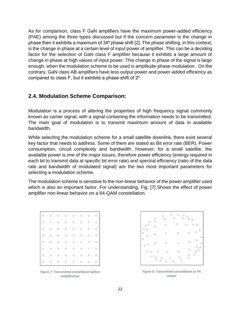
The modulation scheme is sensitive to the non-linear behavior of the power amplifier used
which is also an important factor. For understanding, Fig. [7] Shows the effect of power
amplifier non-linear behavior on a 64-QAM constellation.
Figure 7: Transmitted constellation before
amplification Figure 6: Transmitted constellation at PA
output
23
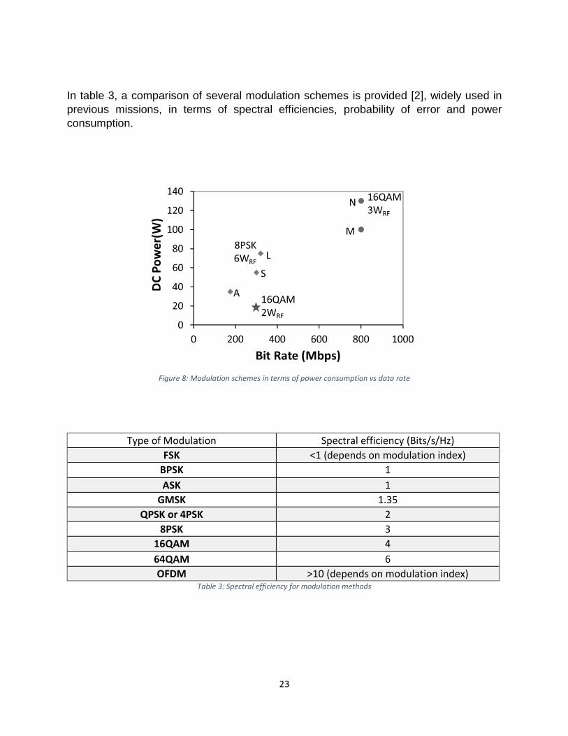
In table 3, a comparison of several modulation schemes is provided [2], widely used in
previous missions, in terms of spectral efficiencies, probability of error and power
consumption.
Figure 8: Modulation schemes in terms of power consumption vs data rate
Type of Modulation Spectral efficiency (Bits/s/Hz)
FSK <1 (depends on modulation index)
BPSK 1
ASK 1
GMSK 1.35
QPSK or 4PSK 2
8PSK 3
16QAM 4
64QAM 6
OFDM >10 (depends on modulation index) Table 3: Spectral efficiency for modulation methods

24
Figure 9: 16 QAM performance in presence of non-linear amplifier with or without predistortion
From the figure [9], it can be clearly observed that data predistorter can mitigate the
amplifier’s non-linear behavior effects. Predistorter can considerably reduce the
amplitude compression and phase rotation which is caused by the power amplifier.
However, from the above analysis it is resulted out that in view of the project requirements
and specifications, the 16 QAM modulation scheme is a better option to adopt with respect
to its power consumption and nominal spectral efficiency. Although there is new and more
recently developed modulation scheme known as adaptive modulation technique can also
be considered for the small satellite downlink communication. This method has the
tendency to adopt the modulation scheme (M-QAM of interest depending on the current
conditions of channel such as amplifier back-off, SNR levels and fading characteristics.
Eventually, by the use of this technique improvement can be made in power and spectral
efficiencies as well as non-linear distortion and inter-symbol interference can also be
reduced.
Fig.10 shows [7] the channel capacity when the adaptive modulation technique is applied
with combination of predistortion method.

25
Figure 10: Modulation Schemes comparison in terms of Average SNR vs Capacity
2.5. Doppler Effect for LEO satellites:
Doppler shift is a phenomenon of a change in frequency which is observed when an object
moves towards or away from the observer. In case of satellite communication, the object
is satellite and observer is the ground station/terminal.
During satellite communications, the radio waves are affected by the Doppler
phenomenon. Although it is small for the communications using lower frequency i.e. few
Hz for a VHF mobile receiver. But it becomes significant while the use of SSB (Single
Side Band) operations. Doppler shift is directly proportional to the operating frequency
which means it is more significant (needs to be compensated) on UHF. Furthermore, its
effect on communication depends on the type of modulation scheme, multiplexing
techniques and satellite access methods.
The Doppler Effect becomes more substantial during the case of lower earth orbit
satellites. Because the LEO satellites are moving at a velocity near to 7.5 Km/s relative
to earth’s surface. For the users on the ground, the Doppler shift frequency changes when
the satellites passes overhead. In most cases, it depends on the orbital geometry on the
satellite and the latitude and longitude of the ground terminal. The pass of the satellite is
divided into two section depending on the elevation angle and viewing point of the ground
observer. If the satellite is ascending part of the orbit, then ground observer can notice
the maximum frequency shift when the satellite appears at south horizon and it goes on
decreasing to minimum value until the satellite reaches north horizon. Similarly if the
satellite is in descending part of the orbit, the frequency shift maximizes at the north
horizon with respect to the ground terminal/observer.

26
In the figure [11], the change in Doppler frequency shift for a satellite (typical iridium
satellite) overhead pass with respect to the ground station is shown. The pass starts as
the satellite appears to be rising above the horizon until it disappears.
Figure 11: Doppler Frequency Shift Curve
To calculate the Doppler rate, we can take the derivative of above curve with respect to
time and the resultant is shown in the Fig.12 [9].
Figure 12: Doppler Rate Curve

27
The Doppler shift for a circular orbit with relation to the height of the satellites ‘orbit can
be given by
∆𝑓𝐷 = 𝑓0𝑣𝑑
𝑐
Where 𝑣𝑑 can be given as:
𝑣𝑑 = ⌈ √𝜇𝑟𝑒
2
(𝑟𝑒 + ℎ)3cos 𝛾 sin 𝜑 −
2𝜋
86164𝑟𝑒 cos 𝑙𝑡 cos 𝛾 cos 𝜑 ⌉
In the above equation, 𝑙𝑡 is defined as the latitude of the ground terminal whereas 𝜑 is
the angle between latitudinal tangent at sub satellite point and terminal projection line
onto the tangential plane at sub satellite point, 𝑟𝑒 represents the radius of earth, 𝜇 is
defined to the gravitational constant and ℎ is the height of satellite’s orbit.
There are several methods developed for the compensation of Doppler frequency shift
such as:
Closed-terminal satellite frequency control loop
On-board satellite Doppler correction
Pre-correction on the receiver side of the link
Pre-correction on the transmitter side of the link

28
Chapter 03
3.1. Power Amplifier linearization techniques
As discussed in the previous chapters, the working and output behavior of power amplifier
is affected when the power amplifier approaches to its saturation point. The non-linear
behavior of and saturation point relation of power amplifier varies with the type/class and
operating conditions of power amplifier. The most significant signal distortion affects are
harmonic distortion, spectral regrowth and inter-modulation distortions. The distortion not
only affects the clarity of the signal but also creates inter-frequency interference.
However, the main idea is to decrease the non-linearity in PA’s output as much as
possible so that the unwanted intermodulation terms and signal distortion can be reduced
to a minimum level. There are certain parameters for the evaluation of performance and
efficiency of power amplifier, such as, NMSE, ACLR and power spectrum mask. These
factors evaluate the working of power amplifier, for example, normalized mean square
error defines the estimated deviation of output signal with respect to the input signal. It
should be kept to a level of -35 dB to -40 dB to represent the comparison of input and
output signal of power amplifier. It shows that how much in-band distortion is adding by
the power amplifier and the quantity of change in output signal as compared to input.
Similarly, ACLR (adjacent channel leakage ratio) is defined to be the ratio between
transmitted power and adjacent channel power. The level of this factor is kept to be
between -45 dB to -50 dB for achieving desired results of amplification, linearity of power
amplifier. Power spectral density (PSD) is also a measure of defining the behavior of
power amplifier. With the help of power spectrum mask, the amplification occurred in out-
of-band signal and in-band can be noticed. This master thesis will be focusing on these
parameters for determining the behavior of power amplifier as well as the designed
predistortion system.
For the said purposes, a signal must be well operated and gone through several
procedures before inputting it to the power amplifier so that the desirable level of linearity
can be achieved. These schemes and procedures varies with the requirement of projects
in which power amplifier needs to be used. The deriving parameters can be efficiency,
channel interference, wider bandwidth, and complexity and modulation methods. In the
field of digital signal processing, extensive research has been made in past to formulate
different methodologies for countering the non-linear effect of power amplifier. Resulting
in various PA linearization schemes, where each of them has its own advantages and
flaws.
However, there is not a single methodology which can work in different set of
circumstances. Some of these schemes are elaborated in this report which are applicable
in several situations. Ending with one of the mostly researched and stable method
29
(predistortion) which is also applied in this particular Master thesis to achieve the desired
results.
3.2. Methods to compensate Non-linearity in PA behavior
Few commonly known/researched Power amplifier linearizer methods are enlisted below
with a comprehensive description of each.
FEED BACK
FEED FORWARD
PREDISTORTION
3.2.1. Feed Back system:
The feedback system technique is the most commonly used method to make the PA
behavior linear to a certain level. This technique can have various shapes depending on
the various types of feedback systems used. Some extensively used categories of this
methodology are local feedback system, global feedback system, baseband feedback
system, Cartesian feedback system and polar feedback system.
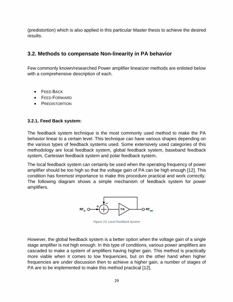
The local feedback system can certainly be used when the operating frequency of power
amplifier should be too high so that the voltage gain of PA can be high enough [12]. This
condition has foremost importance to make this procedure practical and work correctly.
The following diagram shows a simple mechanism of feedback system for power
amplifiers.
Figure 13: Local Feedback System
However, the global feedback system is a better option when the voltage gain of a single
stage amplifier is not high enough. In this type of conditions, various power amplifiers are
cascaded to make a system of amplifiers having higher gain. This method is practically
more viable when it comes to low frequencies, but on the other hand when higher
frequencies are under discussion then to achieve a higher gain, a number of stages of
PA are to be implemented to make this method practical [12].

30
Figure 14: Global Feedback System
The implementation of baseband feedback system is shown in the Fig.15. The idea in this
method is to feedback the baseband signal to the input instead of RF signal. As the
bandwidth of baseband signal is much lower than RF signal, therefore, the bandwidth
requirement in the feedback loop can be reduced by performing it [12]. This method is
more applicable in the conditions of higher frequency bands or larger bandwidths. On the
other hand, this method is more complex.
Figure 15: Baseband Feedback System [12]
3.2.2. Feed forward System:
The feed forward system is also a commonly used linearization method under a set of
certain circumstances. Mainly this method uses the two loops of distortion cancellation
mechanism as can be seen in the following diagram.
The main course of action in this system is to achieve only the distortion at the output of
first loop of cancelling mechanism by minimizing the gain and tweaking the phase of input
signal. As the distortion is known then the original signal can be subtracted from it to
obtain an amplified and non-distorted output signal.

31
Figure 16: Feed Forward Linearization System
The feed forward system is suitable choice for in band amplitude and phase distortion
correction. One of the benefits of this system is its inherited stability. However, this can
be a viable approximation method when the bandwidth of modulated carrier is small as
compared to the frequency of carrier [12].
3.2.3. Predistortion:
The predistortion is a most commonly and widely used/researched method for linearizing
the behavior of non-linear RF power amplifier. The RF or baseband signal can be treated
before inputting to the RF power amplifier by a cost-effective and efficient method known
as digital predistortion. However, there can more than one ways to implement the
predistortion technique. Either the amplitude/ phase of RF signal can be predistorted
before it passes to the RF amplifier or the predistortion of baseband input signal can be
performed to directly nullify the power amplifier’s distorted performance [15].
Figure 17: Predistortion before Modulation
Figure 18: Predistortion after Modulation

32
Furthermore, the predistortion method can be applied in various forms depending on the
requirement/specification of the project. These forms can be open loop predistortion,
closed loop, iterative/adaptive feedback and memoryless/with memory effect. Although
with the enhancement in the efficiency of a system the method becomes more complex
in terms of model estimation and hardware implementation yet manageable.
Figure 19: Closed Loop Predistortion [12]
Basically, the digital Predistortion method deals with the modelling of RF PA behavioral
characteristics but inverse in nature. This method changes the signal before amplification,
counter the effects the of distortion produce by PA, eventually obtaining a clear and
distortion-less signal at the output of PA. From the implementation point of view, an
estimated prediction of power amplifier behavior is modelled by using the polynomial
expressions. Then inverse replica of the modelled data is generated to perform the
inverse operation on the baseband or RF signal before inputting it to the power amplifier
(as can be seen in Fig. 20).
Figure 20: Predistortion System
The predistortion scheme can be developed and implemented in both analog and digital
domain. Predistortion in both domain have their own advantages as well as
disadvantages. There are transceivers with capability to perform digital to RF conversion
on a single chip which can reduce the cost and save the space as well as power
consumption. With the advantage of using digital predistortion for the linearity of power
amplifier, there also exists a drawback. The predistortion causes the increase in the
bandwidth to at least five times of its original bandwidth. This phenomenon is termed as
33
bandwidth expansion. Due to exhibition of this phenomenon, the digital to analog
converter, implemented at the output of predistortion, has to be designed at a sampling
frequency of five times greater than the original bandwidth of the signal. This causes the
complexity in the design of DAC and also hardware implementation becomes challenging.
This master thesis involves in design of such cooperative scheme of digital and analog
predistortion that can counter the aforementioned problem.
3.2.3.1 Predistortion System Configurations:
Accurate modelling of PA is the foremost step in designing of predistortion system. The
better the model of PA is the better designing of PD (Predistortion) system can be done.
As far as modelling is concerned, there exists several mathematical model to simulate
the behavior of power amplifier. These models are different in nature regarding hardware
implementation complexity, memory effects execution and polynomial orders. The
selection of model is mostly dependent on the requirements of the assignment and
available resources.
This Master Thesis deals with a combination of Digital and Analog (Simulated)
predistortion system. The PA model selected for designing this system is based on the
Dynamic Deviation Reduction (DDR) Volterra series which is a reduced and truncated
form of original Volterra series. The Volterra series provides a general input output
relationship of power amplifier behavior with the involvement of memory effect. But due
the high level of implementation complexities (because of exponential increase in the
number of parameters with the increase in memory length and non-linearity degree) [19],
the general form of Volterra series is truncated and reduced to DDR Volterra series for
making it practically feasible for hardware implementation. The details related to Volterra
series and parameters involved is provided in the upcoming chapters.
While referring to the predistortion system designing, certain parameters/processes in
both domains (digital and analog) are introduced for making the whole system response
more linear and efficient. These parameters consists of implementing the PA model with
memory effects or without memory effect. The static or adaptive are the two process
involves in designing the predistortion system. The memory effects and static/adaptive
schemes are elaborated below in detail.
3.2.3.2 Memory/Memoryless Effect:
This term is used in reference to power amplifier response when the output of PA is no
more dependent on the instantaneous input but also caters the effect of previous inputs
applied to it. This effect is quite important to consider while modelling of PA. Although it
does not directly affect the linear behavior of amplifier yet it influences the complexity and

34
linearity of the transmission system causing an effect on the predistortion linearization
[20].
Most commonly used way to analyze the behavior of PA is the static AM-AM curves and
AM-PM curves. For the case of memoryless system, these static curves and the
predistorter coefficients/gain values can be stored and utilized again to achieve the
desired linear response from non-linear PA. But with the conversion/upgradation of
wireless system to wider bandwidths, higher frequencies and higher data rates it is almost
impossible to model static AM-AM and AM-PM curves for a non-linear power amplifier.
Static modeling can be applied to the narrow bandwidth scenarios but it is no longer
applicable to the wider modulation bandwidths and the memory effect is no longer
negligible in this particular case. From the experimentation in past, it has been seen that
the PA show the memory effects when the bandwidth becomes wider than 20 MHz.
Figure 21: Memoryless Vs Memory polynomial Analysis Diagram
Fig.21 from the previous research [21] elaborates the on the spectra of output signal when
using a memory polynomial based PA model, memoryless model and without Digital
Predistortion system. In Fig.21, it can be seen that the curve (a) gives the most
appropriate and with least out of band distortion amplification as compared to (b) and (c)
curves which represents the memoryless polynomial predistorter and without
predistortion system respectively. As it was commented before, Fig.21 proves that, after
a certain wideness of bandwidth it is necessary to counter the effect of memory issue for
achieving better results in amplification.
Generally, PA behavioral modelling can be classified into three categories based on the
memory effects in the system. Firstly there comes the nonlinear memoryless system

35
which is represented with the AM-AM curves of narrow band signal. Secondly, there is
quasi-memoryless non-linear system which is dependent on the order of period of RF
carrier having memory time constants. Lastly, with memory non-linear system having a
long term memory effect depending on the order of period of envelope signal [22]. In this
thesis, the focus of work is on the third category of the PA behavioral modelling (non-
linear systems with memory effect) by applying the DDR Volterra series model.
There exists a number of causes for the occurrence of memory effect in the behavior of
power amplifier depending whether the memory effect is rather linear or non-linear. The
linear memory effect can be caused due to the time delays among the various instruments
of the system or it can be produced because of phase shifts between the devices used
or matching networks. On the other hand, the non-linear memory effects occurred due
to the temperature influenced by the input power, network biasing and trapping effect [19]
(associated to both surface and layer, gate lagging is incorporated in surface trapping
whereas the drain current collapsing is demonstrated as layer trapping effect).
3.2.3.3 Static/Adaptive Predistortion System:
The predistortion system can be designed on the concept of two approaches namely
static design and adaptive design. The earlier design is easy in terms of implementation
and complexity as compared to the later one.
Static predistortion system is time independent and it involves the modelling of PA
behavior at a certain time instant. After finding the parameters for the predistorter, it is
multiplied with the original signal to incorporate the inverse properties of PA into the
signal. The parameters of PD remains same for every signal assuming that the behavior
of PA is constant over a certain period of time. Linearization in the output signal can be
achieved up to some extent with the help of this design. But with the passage of time and
the changes occur in the behavior of PA like heating or ageing of amplifier and
introduction of memory effect due to time delays, this method becomes more vulnerable
to distortion and turn out to be less efficient.
The static PD can be designed by making inverse model of PA and using it with the
original signal or can be designed with the implementation of look-up tables in which PD
parameters are stored already. The Fig.22, Fig.23 shows the implementation of both
methods on the block level.

36
Figure 22: Static Predistorter
Figure 23: Static Predistorter with LUT [23]
Adaptive predistortion system, on the other hand, is more complex and requires more
processing than the static but it is more prevailing and immune to the out-of-band
distortions. This method can be implemented with several iterative algorithms such as
least square (LS), least mean square (LMS) and recursive least square (RLS). These
algorithms can be selected on the basis of parameters like calculation of quadratic error,
amplitude and phase error and ACPR (Adjacent channel power ratio).
The adaptive system is a more apposite preference because it is time dependent (doesn’t
depend on the instantaneous input but also on the past inputs/outputs) and counters the
effect of ageing, heating and similar parameter of PA. With this system the predistorter
parameters alter in every iteration making the whole system more linearized. Below
mentioned block diagram shows a process of complete scenario for linearizing PA output
with the involvement of adaptation algorithm in the feedback loop.
Figure 24: Adaptive predistortion system [24].
The basic concept of designing an adaptation algorithm is to calculate the error among
the input and output of the system and after processing, update the DPD parameters

37
accordingly. The DPD updater takes the error, output and input signal to find out the
updated coefficients of DPD and feed it to the DPD function in every iteration. This
process takes place until the desired output is achieved and the system converges.
Following diagrams illustrates the least mean square method for adaptation and the
complete system level design respectively.
Figure 25: Adaptive predistortion algorithm block diagram

38
Chapter 04
4.1. Implementation of Adaptive DPD Algorithm
This chapter of Master thesis comprises of the modelling of power amplifier behavior by
the use of DDR Volterra series, designing of digital predistortion (system function and
parameters calculation) and constructing an adaptive algorithms for the feedback system.
As discussed in the previous chapters, the use of DPD is to linearize the output of PA by
introducing the inverse properties of PA to the signal, the similar approach is considered
to design the DPD. The results are shown with descriptive analysis on the basis of AM-
AM and AM-PM curves where required.
4.2. Design and Implementation Procedure:
The purpose is to design a Digital predistortion system that can accurately simulate the
inverses behavior of power amplifier.
Figure 26: Flow diagram of DPD implementation phase

39
The modelling of PA is the first and foremost step in the complete procedure
All the simulation and the results have been compiled in the Matlab Software. The other
steps of the design and implementation phase are presented in the above mentioned flow
chart diagram and explained step by step in the upcoming section of the chapter.
4.3. PA Behavioral Modelling:
An essential and foremost step in designing the complete linearization system mentioned
above is the modelling of power amplifier behavior. The PA modelling, generally, means
to replicate the properties and the effects that a power amplifier can have on a signal
when passes through it. In the case of power amplifier, the mostly observed property is
the non-linearity introduced in the original signal at the output PA. Concluding, it can be
said that the behavioral modelling of PA is the accurate simulation for the non-linearity of
power amplifier. These models are based on software simulations including efficient
computational algorithms so that the relation between input and output of PA can be
described (in terms non-linearity) without the use of a physical instrument.
For designing the model of a power amplifier, the basic principle is to observe and
measure the PA non-linear behavior and based of the already defined model
architectures take the parameter for the new model. These model are represented
mathematically in the shape of set of equations and applied in designing of
communication systems.
While discussing the PA behavioral modelling it is important to mention that, in
communication system and signal processing research literature, the PA can be modeled
as memoryless as well as with memory effects. The memoryless PA behavioral
modelling, as described in detail in previous chapters, is based on AM-AM and AM-PM
functions/curves which are static in terms of input state (having only instantaneous input).
But with the thermal effect over a long period of time and the dc-biasing circuits time
constants, the memory effects arises in the behavior of power amplifier [25].
Various studies/research had been made, on this issue of non-linear memory effects, in
the literature. Some of the studies shows the reasons of this matter, like in [15] it is
explained that the asymmetric effects is a result of distortion in amplitude of the signal, in
addition, it also produces when they react/interact with AM-AM and AM-PM functions.
Similarly, in [26] the authors categorizes the memory effects into thermal and electrical
classes and explained that the intermodulation asymmetry is the effect of thermal memory
issue.
However, with the study of various reason, it is necessary to formulate such a PA model
which involves the memory issues. For this purpose and for achieving the better efficiency
and linearity in communication system a non-linear memory PA model is used. This thesis
also consist of study and implementation of the digital and analog predistortion system by

40
the use of non-linear memory model of power amplifier. This model is an extraction and
truncation of the original Volterra series.
Volterra series can be defined as a combination of nonlinear power terms and the linear
convolution terms formulate together to describe the relation between input and output of
RF power amplifier including the memory effects. While commenting on the general
Volterra series, its high computational complexity is a major concern for its
implementation for some applications. This computational complexity comes due to the
increase in number of parameters for this series is exponential with the increase in degree
of non-linearity and memory length. Therefore for making the Volterra series more
applicable and feasible for hardware implementation with ease of computation, it is
truncated to a certain level with which the PA behavior model is not affected much due to
neglecting the higher order term. This report involves the implementation of such
technique called as Dynamic Deviation Reduction Volterra Series.
The basic concept of reduction applied here is by assuming that the memory duration of
device as compared to signal period is short enough so that the original Volterra series
can be truncated into single integral term that can provide the modelling of weak as well
as strong non-linearities in the amplifier behavior [27] the general form of Volterra series
can be mathematically represented in discrete form as follows.
𝑦(𝑛) = ∑ ∑ … … ∑ ℎ𝑝
𝑀
𝑖𝑝=0
𝑀
𝑖1=0
𝑃
𝑝=1
(𝑖1 … … … 𝑖𝑝) ∏ 𝑥(𝑛 − 𝑖𝑗)𝑝
𝑗=1
Here x(n) is the input signal whereas y(n) is the output. The Volterra kernel are
represented in the equation by ℎ𝑝(𝑖1 … … … 𝑖𝑝) and the order kernel order is ‘p’. P is
denoting the order of non-linearity and M shows the memory length for a given system in
which the mathematical model is applied.
In several applications, the memory length can be truncated to a finite number. With applying the truncation and combining the deviation reduction function the Volterra series can take the form as following.
The deviation reduction function can be represented as
𝑒(𝑛, 𝑖) = 𝑥(𝑛 − 𝑖) − 𝑥(𝑛)
Which is representing the deviation of delayed signal x (n-i) with respect to x(n) [27]. As
the output signal has two elements (static and dynamic), therefore

41
𝑦(𝑛) = 𝑦𝑠(𝑛) + 𝑦𝑑(𝑛)
And consequently,
𝑦(𝑛) = ∑ 𝑎𝑝(𝑛) 𝑥𝑝(𝑛) + ∑ 𝑥𝑝−1(𝑛) ∑ 𝑔𝑝1(𝑖)𝑒(𝑛, 𝑖)
𝑁−1
𝑖=0
𝑃
𝑝=1
𝑃
𝑝=1
The memory effect has a tendency to decrease with the passage of time which concludes
that the longer the time-delayed input signal is the less effect it has on the output of
amplifier with respect to memory [27]. Therefore, by apply the deviation reduction and
truncation to the second order, the Volterra model can be represented as
∑ 𝑎𝑝(𝑛) 𝑥𝑝(𝑛) +
𝑃
𝑝=1
∑[ 𝑥𝑝−1(𝑛) ∑ ℎ𝑝1(𝑖)𝑥(𝑛 − 𝑖)
𝑁−1
𝑖=1
]
𝑃
𝑝=1
+ ∑[𝑥𝑝−2(𝑛) ∑ ∑ ℎ𝑝2(𝑖1, 𝑖2)𝑥(𝑛 − 𝑖1)𝑥(𝑛 − 𝑖2)
𝑁−1
𝑖2=𝑖1
𝑁−1
𝑖1=1
]
𝑃
𝑝=2
The final form of DDR Volterra series is implemented in Matlab and the results are
obtained for the model of power amplifier. The results shows the promising behavior
modeling of the non-linearity introduce by the PA in original input signal which is then
further used for the designing of digital predistortion system.
The behavior of power amplifier is shown with the respect of AM/AM graphs and the
frequency spectrum in the following diagrams for memoryless model and model including
memory effects. The Volterra series model shows quite promising value of normalized
mean square error (NMSE) between the predicted output and the output achieved from
the modelled PA.
42
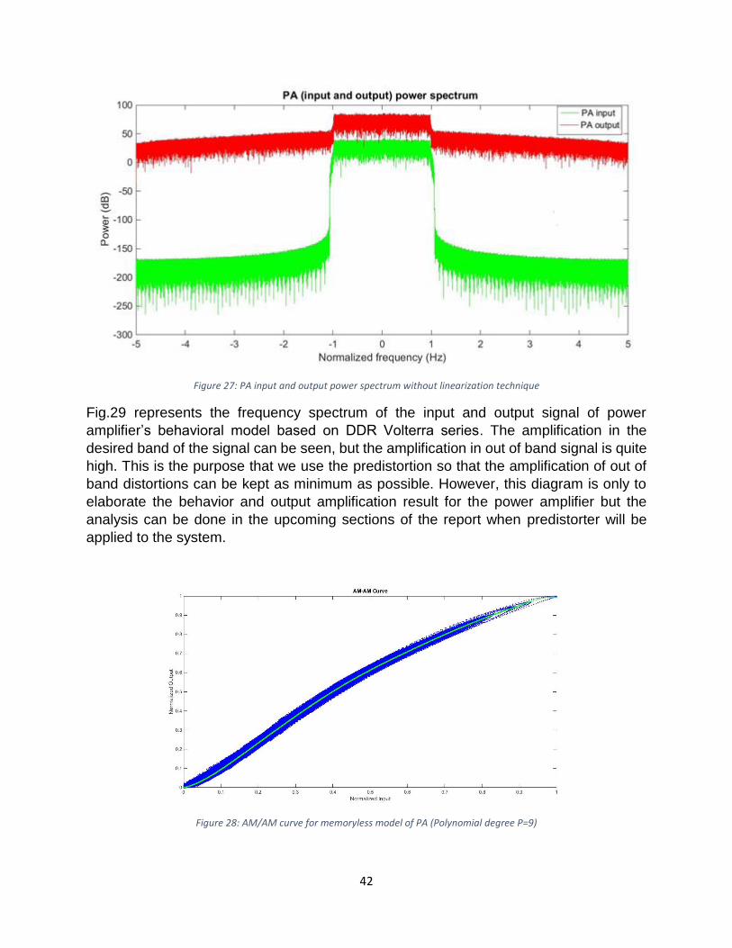
Figure 27: PA input and output power spectrum without linearization technique
Fig.29 represents the frequency spectrum of the input and output signal of power
amplifier’s behavioral model based on DDR Volterra series. The amplification in the
desired band of the signal can be seen, but the amplification in out of band signal is quite
high. This is the purpose that we use the predistortion so that the amplification of out of
band distortions can be kept as minimum as possible. However, this diagram is only to
elaborate the behavior and output amplification result for the power amplifier but the
analysis can be done in the upcoming sections of the report when predistorter will be
applied to the system.
Figure 28: AM/AM curve for memoryless model of PA (Polynomial degree P=9)
43
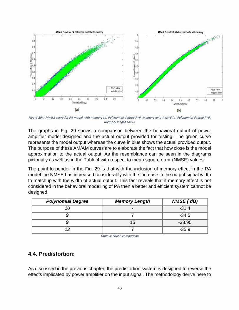
Figure 29: AM/AM curve for PA model with memory (a) Polynomial degree P=9, Memory length M=6 (b) Polynomial degree P=9, Memory length M=15
The graphs in Fig. 29 shows a comparison between the behavioral output of power
amplifier model designed and the actual output provided for testing. The green curve
represents the model output whereas the curve in blue shows the actual provided output.
The purpose of these AM/AM curves are to elaborate the fact that how close is the model
approximation to the actual output. As the resemblance can be seen in the diagrams
pictorially as well as in the Table.4 with respect to mean square error (NMSE) values.
The point to ponder in the Fig. 29 is that with the inclusion of memory effect in the PA
model the NMSE has increased considerably with the increase in the output signal width
to matchup with the width of actual output. This fact reveals that if memory effect is not
considered in the behavioral modelling of PA then a better and efficient system cannot be
designed.
Polynomial Degree Memory Length NMSE ( dB)
10 - -31.4
9 7 -34.5
9 15 -38.95
12 7 -35.9
Table 4: NMSE comparison
4.4. Predistortion:
As discussed in the previous chapter, the predistortion system is designed to reverse the
effects implicated by power amplifier on the input signal. The methodology derive here to

44
design the predistortion involves the working of power amplifier in reverse order.
Practically, it is not impossible but as the implementation is done in simulations, therefore,
the reverse working of PA could be executed. The concept used here is to provide the
output signal as input to already designed PA model function and conclude the output.
Figure 30: Implementation of PA Modelling
The AM/AM curve in Fig.31 and Fig.32 represents the inverse behavior of PA which will
be used as the predistortion applied to input signal. PD curves are derived for the various
scenarios such as memoryless predistorter, with short length memory effect and long
length of memory taps.
Figure 31: AM/AM curve, Memoryless DPD with polynomial degree P=9
45
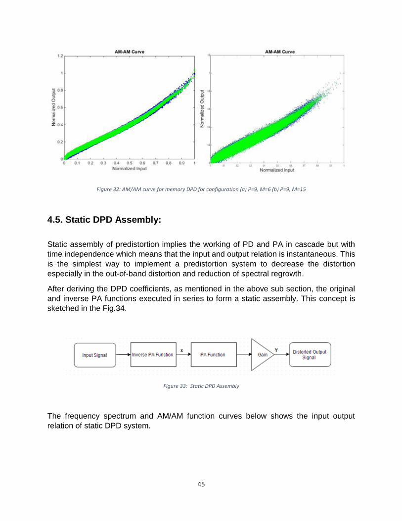
Figure 32: AM/AM curve for memory DPD for configuration (a) P=9, M=6 (b) P=9, M=15
4.5. Static DPD Assembly:
Static assembly of predistortion implies the working of PD and PA in cascade but with
time independence which means that the input and output relation is instantaneous. This
is the simplest way to implement a predistortion system to decrease the distortion
especially in the out-of-band distortion and reduction of spectral regrowth.
After deriving the DPD coefficients, as mentioned in the above sub section, the original
and inverse PA functions executed in series to form a static assembly. This concept is
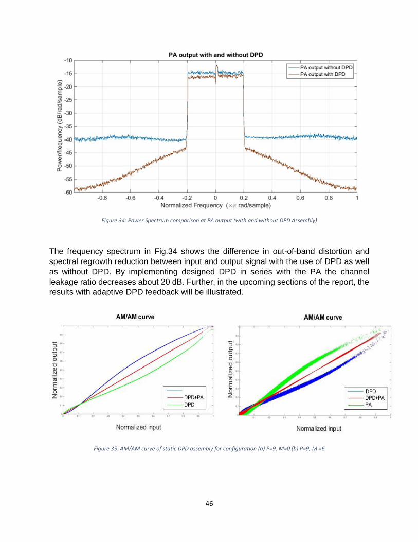
sketched in the Fig.34.
Figure 33: Static DPD Assembly
The frequency spectrum and AM/AM function curves below shows the input output
relation of static DPD system.
46
Figure 34: Power Spectrum comparison at PA output (with and without DPD Assembly)
The frequency spectrum in Fig.34 shows the difference in out-of-band distortion and
spectral regrowth reduction between input and output signal with the use of DPD as well
as without DPD. By implementing designed DPD in series with the PA the channel
leakage ratio decreases about 20 dB. Further, in the upcoming sections of the report, the
results with adaptive DPD feedback will be illustrated.
Figure 35: AM/AM curve of static DPD assembly for configuration (a) P=9, M=0 (b) P=9, M =6

47
Chapter 05
5.1. Web Lab setup for PA Predistortion implementation
The remote setup including power amplifier and analyzing instruments are used for
implementing and testing the predistortion system designed in previously. The adaptive
predistortion system is designed in addition to the previously build setup for reducing the
spectral regrowth and distortion among output of PA.
This remote setup is known as Web Lab which was structured by University of Chalmers
(Sweden) and National Instruments. This web Lab is provided to the students for testing
the linearizing algorithms on hardware by accessing it remotely online. This setup is
consisted of a signal generator, Non-linear GaN power amplifier and signal analyzer.
Figure 36: Web Lab Instruments [28]
The use of Web lab platform can be performed in two separate ways. One method is to
upload the data to the server of Web Lab and it will process the data and compile the
results in some time and the analysis can be done on these results afterwards. The other
methodology to access the web Lab is the dedicated m.file (Matlab file) on to the personal
computer and use it for compiling the results. There is no restriction for any user for the
use of these instruments but few parameters are needed to be kept in mind before
uploading the data to access the Web Lab. These parameters includes PAPR and RMS
power levels of the signal. The test signal used for the obtaining results in various
experimentation scenarios is an OFDM-like signal with a bandwidth of 40 MHz.

48
5.2. Adaptive Predistortion Implementation through Web Lab
As discussed in the previous chapters, the adaptive predistortion is a setup in which
iteration procedure is applied to calculate the error signal at the output of power amplifier
and utilize it to calculate new coefficients for predistorter in each iteration to make it better
and efficient in terms of linearity. Therefore, the adaptive system is developed with the
use of Least Square approach. The concept of the system is sketched in the below
diagram on a block level.
Figure 37: Adaptive DPD Block Diagram
In Fig.37, U represents the input signal given to the digital predistorter designed
previously. The least square method for the adaptive predistortion system can be
expressed mathematically as follows.
In Fig.37, X shows the output of digital predistortion that can be represented
mathematically as
𝑥(𝑛) = 𝑢(𝑛) − 𝑑(𝑛)
𝑑(𝑛) = 𝜱𝒏 𝒘𝒏
𝒘𝒏 = (𝛼00 … . 𝛼0𝑃 … . 𝛼𝑁0 … . 𝛼𝑁𝑃)
𝑢(𝑛) is the original input signal and 𝑑(𝑛) is the data matrix obtained after inputting the
signal to the DPD function 𝛷𝑛 and multiplying with the coefficient of DPD i.e. 𝑤𝑛 . 𝑤𝑛 is
dependent on the polynomial degree P and number of memory taps N. After deriving x(n),
it is inputted to amplifier and an output y is obtained. The error signal is obtained by using
49
the following expression which leads to the calculation of new coefficients of DPD for the
next iteration.
𝑒(𝑛) = 𝑦(𝑛)/𝐺0 − 𝑢(𝑛)
Where 𝑒(𝑛) represents the error signal, 𝑦(𝑛) and 𝑢(𝑛) is the output and input respectively
and 𝐺0 is the gain. Once the error signal is obtained, new coefficients for DPD are
calculated through following equations. The well-known least-squares solution for
feedback system and obtaining the new coefficients in every iteration is mathematically
expressed as
𝒘𝒏+𝟏 = 𝒘𝒏 + ʎ 𝜟𝒘𝒏
𝜟𝒘𝒏 = (𝜱𝑯𝜱)−1𝜱𝑯𝑒
In the first iteration the DPD will consider the coefficients as zeros and provide and input
X to the power amplifier. After amplification, the preprocessor will up sample and align
the signal for the use in next iteration. The DPD updater block will calculate the error
signal by comparing the input and output and further use it to calculate the new DPD
coefficients. These coefficients will be used in digital predistorter for the next iteration.
The same procedure will keep on continuing until the desired ACLR or NMSE values are
achieved.
The AM/AM curves and frequency spectrum is calculated by using this procedure and
shown in Fig. 38. These graphs are derived on different degrees of polynomial and
memory length for analyzing the effect of these parameters on the linearity and efficiency
of power amplifier output.

50
Figure 38: AM/AM curves, Memoryless Adaptive DPD (Polynomial degree P=9)
Figure 39: Memoryless DPD (input and output) power spectrum
51
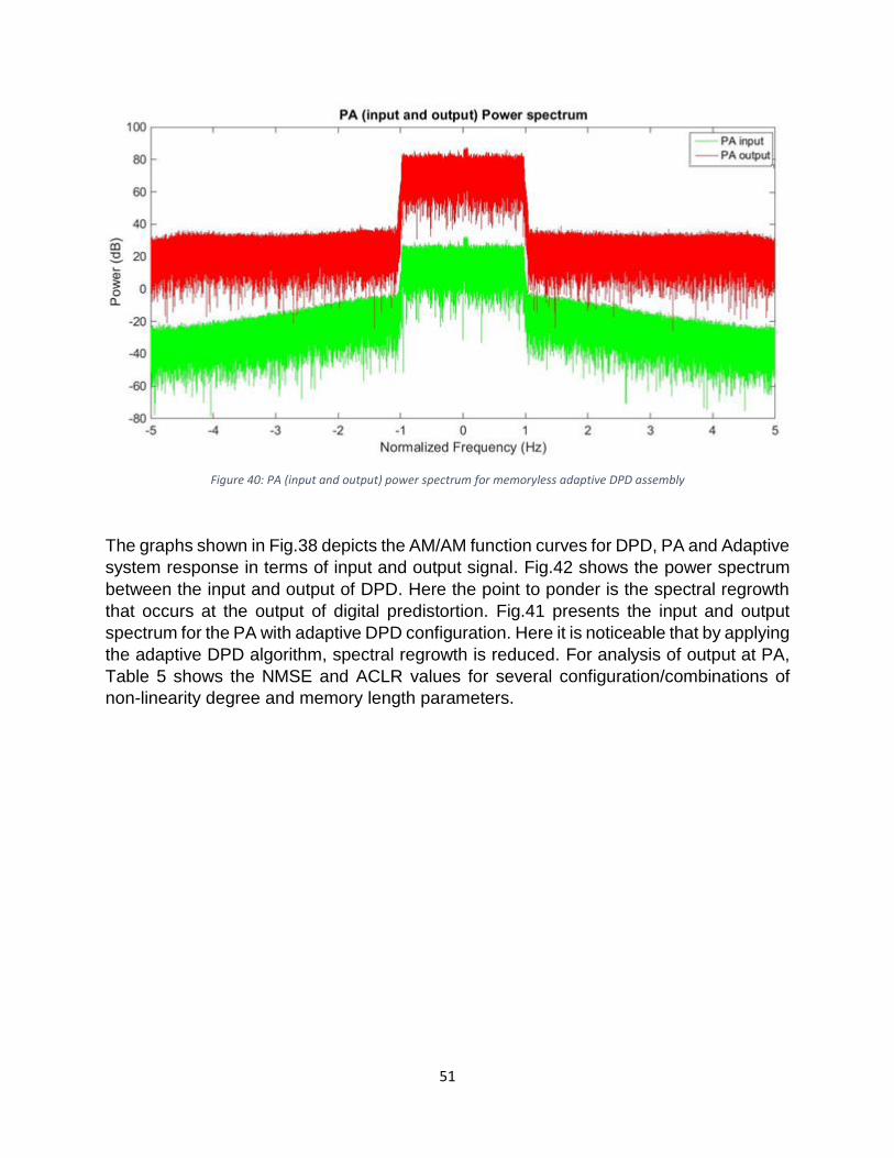
Figure 40: PA (input and output) power spectrum for memoryless adaptive DPD assembly
The graphs shown in Fig.38 depicts the AM/AM function curves for DPD, PA and Adaptive
system response in terms of input and output signal. Fig.42 shows the power spectrum
between the input and output of DPD. Here the point to ponder is the spectral regrowth
that occurs at the output of digital predistortion. Fig.41 presents the input and output
spectrum for the PA with adaptive DPD configuration. Here it is noticeable that by applying
the adaptive DPD algorithm, spectral regrowth is reduced. For analysis of output at PA,
Table 5 shows the NMSE and ACLR values for several configuration/combinations of
non-linearity degree and memory length parameters.
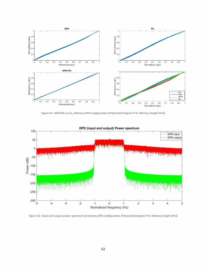
52
Figure 41: AM/AM curves, Memory DPD configuration (Polynomial Degree P=9, Memory length M=6)
Figure 42: Input and output power spectrum of memory DPD configuration (Polynomial degree P=9, Memory length M=6)
53
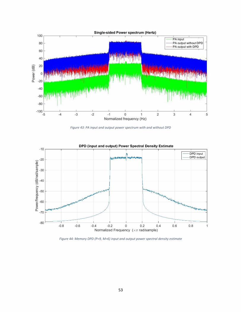
Figure 43: PA input and output power spectrum with and without DPD
Figure 44: Memory DPD (P=9, M=6) input and output power spectral density estimate

54
Figure 45: PA input and output power spectral density estimate with and without DPD
Polynomial Degree Memory Length NMSE (dB) ACLR (dB) Output Power (dBm)
9 - -35.0406 -48.2395 27.2212
9 5 -40.5993 -48.0154 27.3269
9 15 -40.7230 -48.0638 27.3054
Table 5: Memory length effects on important parameters
Figure 46: AM/AM curve for Memory DPD and PA behavioral model with Polynomial degree P=9, Memory length M=15
55
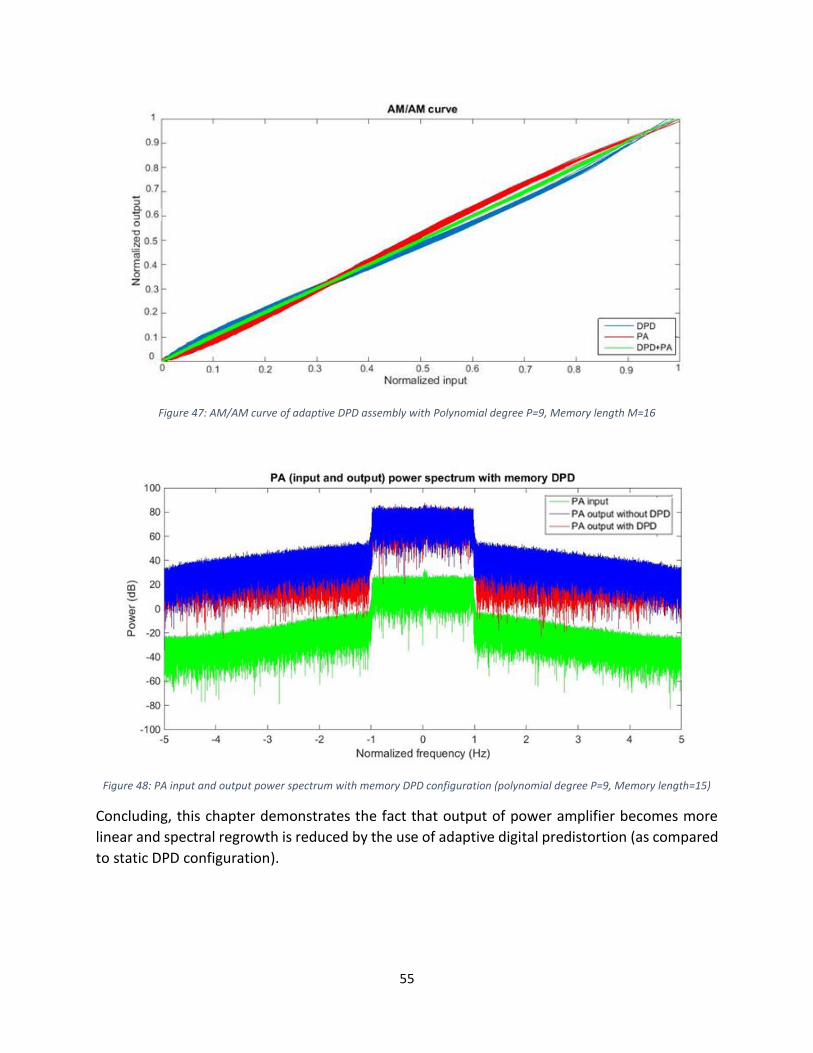
Figure 47: AM/AM curve of adaptive DPD assembly with Polynomial degree P=9, Memory length M=16
Figure 48: PA input and output power spectrum with memory DPD configuration (polynomial degree P=9, Memory length=15)
Concluding, this chapter demonstrates the fact that output of power amplifier becomes more
linear and spectral regrowth is reduced by the use of adaptive digital predistortion (as compared
to static DPD configuration).

56
Chapter 06
6.1. Cascaded PD Implementation
This chapter represents the concept addressing the problem of bandwidth expansion,
resulting due to the predistortion linearization. As discussed earlier, the digital
predistortion, on one side, removes the non-linearity from power amplifier behavior and
thus making the system response linear. On the other hand, it also introduce the
expansion in the bandwidth of original signal. According to rule of thumb, this expansion
can be up to five times of original signal bandwidth. Due to this problem the digital to
analog converter has to design at a greater sampling frequency which increases the cost
and power consumption of DAC. For example, the bandwidth of the baseband signal is
20 MHz, the bandpass signal’s bandwidth would be equal to 40 MHz. According to nyquist
theorem, the sampling rate will be greater than twice of baseband bandwidth (means
greater than 40 MHz). In the case of spectral regrowth introduced by DPD, the bandwidth
expanded to at least five times, then at input of DAC, the signal bandwidth becomes 100
MHz. Consequently, the DAC has to set the sampling rate of signal at greater the 200
MHz which causes an increase in power consumption of system.
This section of report presents a cooperative scheme of digital and analog predistortion
system with a use of low-pass filter. The resultant of this scheme is that the system
response will be as linear as the use of memory DPD whereas the DAC has to only
sample the signal at the original signal bandwidth instead of five times. This scheme
comprises of a digital with memory predistortion, the output of which is filtered with a use
of digital ideal low-pass filter and cascaded with an analog predistortion. The analog
predistortion, in this case, is essentially a memoryless DPD for countering the effects of
in-band distortion. The analysis of this technique is made on the factors of NMSE, ACLR,
output power of amplifier and the power spectrum mask of output at each stage.
Comparison is performed and presented in terms of aforementioned parameters at each
stage of system.
6.2. Emulated APD design:
Simulation of analog predistortion is designed in Matlab for using it alongside the
cooperative scheme mentioned above. The emulated APD is designed on the principle
of a digital predistortion without the effects of memory. Therefore a static memoryless
DPD is designed with different polynomial degree configuration for obtaining the
maximum level of NMSE, ACLR and output power. The results in Table 6 shows that by
changing the polynomial degree in the DPD design the three parameters has shown some

57
variations. The configuration of APD used in the experimentation is with polynomial
degree P=9.
Polynomial Degree NMSE (dB) ACLR (dB) Pout (dBm)
07 -34.3012 -47.8124 27.3712
09 -34.5870 -47.8615 27.3750
12 -34.6085 -47.9349 27.3770
Table 6: Polynomial degree effects on various parameters
6.3. Low-pass Filter Designing:
An ideal low-pass filter is simulated in Matlab for filtering out the expanded bandwidth as
a result of digital predistortion. The low-pass filter is designed by making a spectrum mask
of 1’s (in magnitude) for the desired passband frequencies and 0’s for the stopband
frequencies. Then after computing the FFT of DPD output signal, apply the mask to it.
After multiplying the ideal filter mask with the DPD output signal, perform the IFFT of
output and feed it to the APD.
The results of low-pass filter is shown in Fig.49 and Fig.50 shows the signals before and
after the application of ideal low-pass filter in logarithmic and linear scale.
Figure 49: Input and output spectrum (after fft) of ideal low-pass filter in logarithmic scale
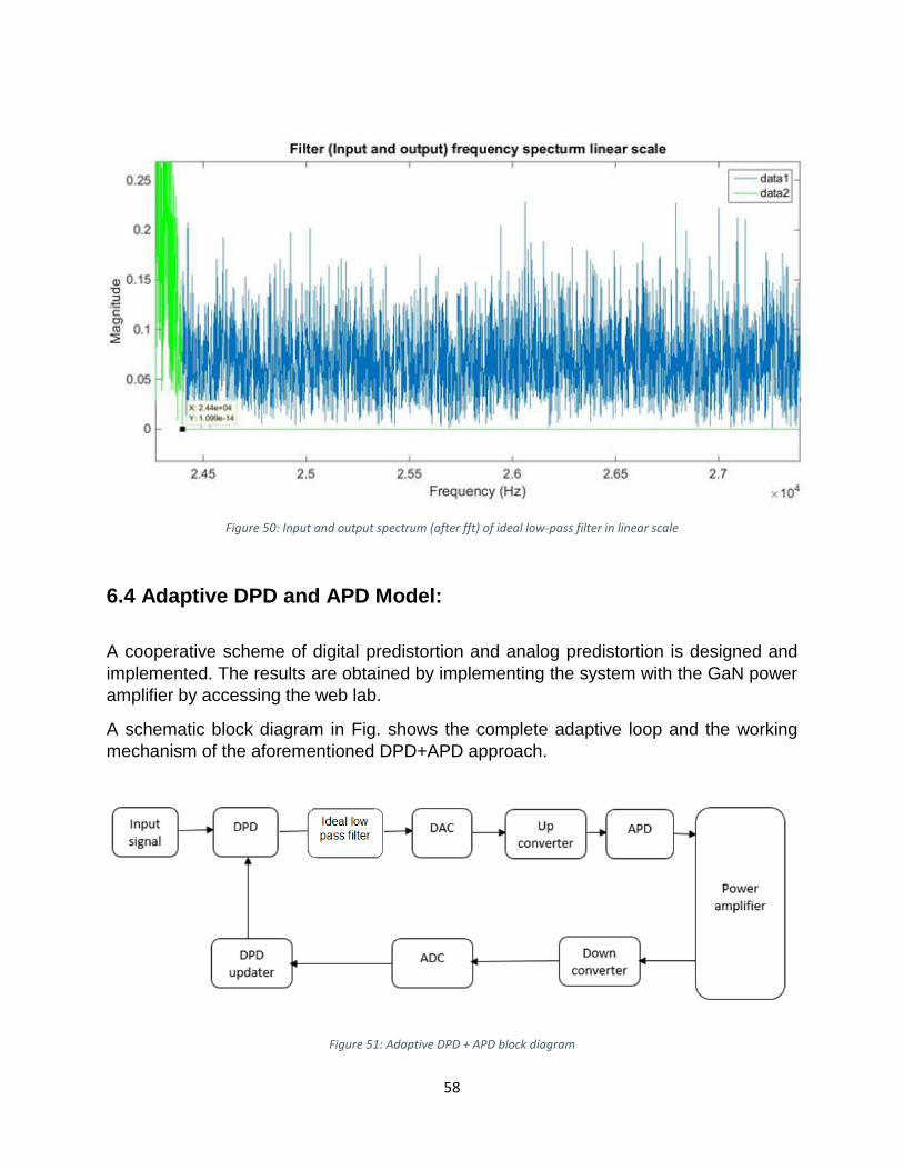
58
Figure 50: Input and output spectrum (after fft) of ideal low-pass filter in linear scale
6.4 Adaptive DPD and APD Model:
A cooperative scheme of digital predistortion and analog predistortion is designed and
implemented. The results are obtained by implementing the system with the GaN power
amplifier by accessing the web lab.
A schematic block diagram in Fig. shows the complete adaptive loop and the working
mechanism of the aforementioned DPD+APD approach.
Figure 51: Adaptive DPD + APD block diagram
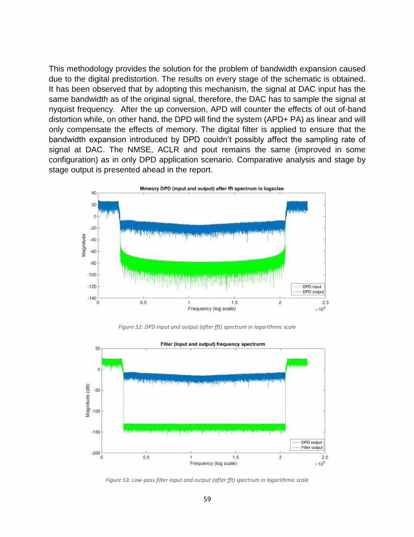
59
This methodology provides the solution for the problem of bandwidth expansion caused
due to the digital predistortion. The results on every stage of the schematic is obtained.
It has been observed that by adopting this mechanism, the signal at DAC input has the
same bandwidth as of the original signal, therefore, the DAC has to sample the signal at
nyquist frequency. After the up conversion, APD will counter the effects of out of-band
distortion while, on other hand, the DPD will find the system (APD+ PA) as linear and will
only compensate the effects of memory. The digital filter is applied to ensure that the
bandwidth expansion introduced by DPD couldn’t possibly affect the sampling rate of
signal at DAC. The NMSE, ACLR and pout remains the same (improved in some
configuration) as in only DPD application scenario. Comparative analysis and stage by
stage output is presented ahead in the report.
Figure 52: DPD input and output (after fft) spectrum in logarithmic scale
Figure 53: Low-pass filter input and output (after fft) spectrum in logarithmic scale

60
Figure 54: APD input and output (after fft) spectrum in logarithmic scale
Figure 55: PA input and output (after fft) spectrum in logarithmic scale
Figures from Fig.52 to Fig.55 shows the signals in frequency domain (after fft) in
logarithmic scale for the illustration of spectral regrowth at every stage of the designed
system. The advantage of using this scheme is that the DAC can now be designed on the
sampling frequency equivalent to original bandwidth. All the provided graphs were taken
with the 9th order polynomial and 7 memory length of the DPD.
In this cooperative scenario, the APD is countering the effects of spectral regrowth,
therefore DPD is not trying to compensate for it and focusing on in-band distortion. This
is the reason that filtering is not done for a lot of out-of-band signal. As shown in Fig.57 if
we use the configuration having only DPD, it can be observed that the spectral regrowth

61
is introduced by the DPD. Whereas by using a combination of DPD and APD (shown in
Fig.56), it is witnessed that there is no spectral regrowth at the output of memory DPD.
Figure 56: DPD input and output PSD spectra in DPD+APD configuration
Figure 57: DPD input and output power spectral density comparison without APD

62
Figure 58: PA input and output power comparison with and without linearization technique application
Figure 59: PA output PSD comparison with and without linearization technique application
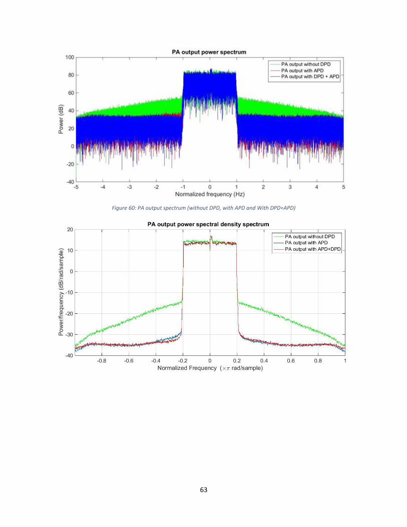
63
Figure 60: PA output spectrum (without DPD, with APD and With DPD+APD)

64
Configuration Bandwidth at DAC
Polynomial Degree
Memory NMSE ( dB)
ACLR( dB)
Pout( dB)
Memoryless DPD
200 MHz 9 0 -34.608 -47.861 27.375
Memory DPD 200 MHz 9 6 -38.523 -47.723 27.371
Memory DPD 200 MHz 9 15 -40.12 -47.785 27.378
Memory DPD + APD
40 MHz 9 6 -39.6793 -47.8002 27.4091
Memory DPD + APD
40 MHz 9 11 -40.0225 -47.9664 27.3303
Memory DPD + APD
40 MHz 9 15 -40.2012 -47.9887 27.4320
Table 7: Final Results for various configurations
Table.7 presents the final results for the cooperative configuration of DPD and APD. The
results have shown that the by using only adaptive DPD, the NMSE reaches up to
maximum of -40 dB while ACLR has the peak value of -47.785 dB. The same results is
observed for the combined configuration of DPD and APD with a low-pass filter between
them. By adopting this methodology, maximum NMSE obtained is noted to be -40.2 dB
which is greater than the only DPD scenario. Further, the ACLR remain approximately on
the same level. The advantage of using this cascaded technique is the bandwidth of signal
at the input of DAC. With the use of only DPD, the bandwidth is at least five times,
therefore, the DAC has to sample the signal at five times of nyquist frequency. But with
the use of cascaded technique, the DAC has to be designed with a sampling rate of
nyquist rate, which is twice of signal bandwidth. These results have shown the promising
behavior of the proposed scheme and can be adopted for improving the system linearity
as well as reduce the signal bandwidth at the input of designed DAC.
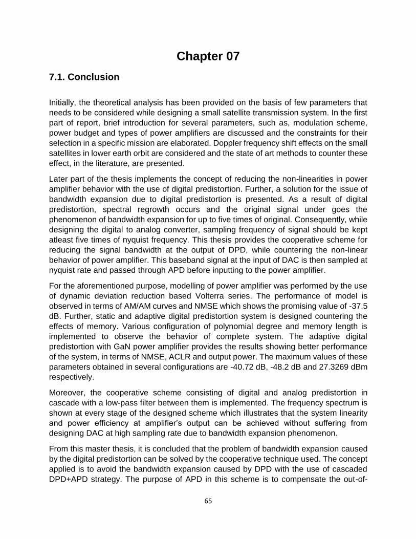
65
Chapter 07
7.1. Conclusion
Initially, the theoretical analysis has been provided on the basis of few parameters that
needs to be considered while designing a small satellite transmission system. In the first
part of report, brief introduction for several parameters, such as, modulation scheme,
power budget and types of power amplifiers are discussed and the constraints for their
selection in a specific mission are elaborated. Doppler frequency shift effects on the small
satellites in lower earth orbit are considered and the state of art methods to counter these
effect, in the literature, are presented.
Later part of the thesis implements the concept of reducing the non-linearities in power
amplifier behavior with the use of digital predistortion. Further, a solution for the issue of
bandwidth expansion due to digital predistortion is presented. As a result of digital
predistortion, spectral regrowth occurs and the original signal under goes the
phenomenon of bandwidth expansion for up to five times of original. Consequently, while
designing the digital to analog converter, sampling frequency of signal should be kept
atleast five times of nyquist frequency. This thesis provides the cooperative scheme for
reducing the signal bandwidth at the output of DPD, while countering the non-linear
behavior of power amplifier. This baseband signal at the input of DAC is then sampled at
nyquist rate and passed through APD before inputting to the power amplifier.
For the aforementioned purpose, modelling of power amplifier was performed by the use
of dynamic deviation reduction based Volterra series. The performance of model is
observed in terms of AM/AM curves and NMSE which shows the promising value of -37.5
dB. Further, static and adaptive digital predistortion system is designed countering the
effects of memory. Various configuration of polynomial degree and memory length is
implemented to observe the behavior of complete system. The adaptive digital
predistortion with GaN power amplifier provides the results showing better performance
of the system, in terms of NMSE, ACLR and output power. The maximum values of these
parameters obtained in several configurations are -40.72 dB, -48.2 dB and 27.3269 dBm
respectively.
Moreover, the cooperative scheme consisting of digital and analog predistortion in
cascade with a low-pass filter between them is implemented. The frequency spectrum is
shown at every stage of the designed scheme which illustrates that the system linearity
and power efficiency at amplifier’s output can be achieved without suffering from
designing DAC at high sampling rate due to bandwidth expansion phenomenon.
From this master thesis, it is concluded that the problem of bandwidth expansion caused
by the digital predistortion can be solved by the cooperative technique used. The concept
applied is to avoid the bandwidth expansion caused by DPD with the use of cascaded
DPD+APD strategy. The purpose of APD in this scheme is to compensate the out-of-

66
band distortion from the RF signal, while DPD is responsible of compensating the in-band
distortions. For the case, when APD is working properly, the DPD will find the system of
APD+PA as linear and only compensate the memory effects introduced by the amplifier.
Then there will be no need to put a filter between DPD and APD, but to make sure that
the bandwidth expansion doesn’t affect the sampling rate of signal at DAC, the low-pass
filter is applied. The results provided in this report has shown that the NMSE, ACLR and
output power of the amplifier remain same or improves (in some configurations) by the
use of this scheme. While the DAC has to operate at sampling rate of original signal
bandwidth rate i.e. if the bandpass is of 40 MHz, then the DAC sampling frequency would
be > 40 MHz.

67
This Page Intentionally Left Blank

68
Bibliography
[1] Sen, Ozlem, Hacer K. Sunay, and Celal Dudak. "An X-band transmitter for satellite
communication." Recent Advances in Space Technologies, 2003. RAST'03. International
Conference on. Proceedings of. IEEE, 2003.
[2] Saito, Hirobumi, et al. "High-speed downlink communications with hundreds Mbps from
50kg class small satellites." 2012IAC, IAC-12-B2 3 (2012).
[3] Clark, Craig S., and Kevin W. Hall. "Power system design and performance on the world's
most advanced in-orbit nanosatellite." Space Power. Vol. 502. 2002.
[4] WATANABE, Hiromi, et al. "Development of high-speed and high-efficiency downlink
transmitter with GaN-HEMT amplifier and predistortion technique for nano/small
satellite."
[5] http://www.sedi.co.jp/pdf/FLM7785-4F.pdf
[6] Mulally, Daniel, and Don Lefevre. "A comparison of digital modulation methods for small
satellite data links." (1991).
[7] Ibnkahla, Mohamed, et al. "High-speed satellite mobile communications: technologies and
challenges." Proceedings of the IEEE 92.2 (2004): 312-339.
[8] Ceylan, Osman, et al. "Low cost S Band communication system design for nano
satellites." Recent Advances in Space Technologies (RAST), 2011 5th International
Conference on. IEEE, 2011.
[9] Ah-Thew, G. "Doppler Compensation for LEO Satellite Communication Systems." (1998).
[10] Ali, Irfan, Pierino G. Bonanni, and Naofal Al-Dhahir. Doppler Applications in LEO Satellite
Communication Systems: CD-Rom Included. Vol. 656. Springer Science & Business
Media, 2001.
[11] Tabaković, Željko. "Doppler effect in non-GSO satellite propagation."Millennium
conference on antennas and oropagation-IEEE AP-2000. Hrvatska znanstvena
bibliografija i MZOS-Svibor, 2000.
[12] Linearization methods Stephen Bruss April 23, 2003
[13] [Fedorenko, Pavlo, and J. Stevenson Kenney. "Analysis and suppression of memory
effects in envelope elimination and restoration (EER) power amplifiers." Microwave
Symposium, 2007. IEEE/MTT-S International. IEEE, 2007.
[14] Kazimierczuk, Marian K. RF power amplifier. John Wiley & Sons, 2014].
[15] Cripps, Steve C. Advanced techniques in RF power amplifier design. Artech House, 2002.
[16] Braithwaite, R. Neil. "Analog Linearization Techniques Suitable for RF Power Amplifiers
Used in Integrated Transmitters." 2013 IEEE Compound Semiconductor Integrated
Circuit Symposium (CSICS). 2013.
69
[17] Kim, Young, Ik-Soo Chang, and Yong-Chae Jeong. "An analog predistortion linearizer
design." Microwave Journal 48.2 (2005): 118-120.
[18] Ben Mabrouk, Mouna, et al. "A novel digital post-distortion and detection technique for RF
power amplifiers in cognitive radio systems." Wireless Symposium (IWS), 2015 IEEE
International. IEEE, 2015
[19] [Zhu, Anding, Jose C. Pedro, and Thomas J. Brazil. "Dynamic deviation reduction-based
Volterra behavioral modeling of RF power amplifiers."Microwave Theory and
Techniques, IEEE Transactions on 54.12 (2006): 4323-4332]
[20] Fedorenko, Pavlo. "Phase distortion in envelope elimination and restoration radio
frequency power amplifiers." (2009).
[21] [Qian, Hua, et al. "Predistortion linearization measurement results for power amplifiers
with memory effects." Proc. IEEE Topical Workshop on Power Amplifiers for Wireless
Communications,(San Diego, CA). 2004]
[22] Ku, Hyunchul, Michael D. McKinley, and J. Stevenson Kenney. "Quantifying memory
effects in RF power amplifiers." Microwave Theory and Techniques, IEEE
Transactions on 50.12 (2002): 2843-2849
[23] http://www.mumor.org/public/deliverables/d36_leti_dr_pu_002.pdf
[24] Montoro, Gabriel, et al. "An LMS-based adaptive predistorter for cancelling nonlinear
memory effects in RF power amplifiers." Microwave Conference, 2007. APMC
2007. Asia-Pacific. IEEE, 2007.
[25] Ku, Hyunchul, and J. Stevenson Kenney. "Behavioral modeling of nonlinear RF power
amplifiers considering memory effects." Microwave Theory and Techniques, IEEE
Transactions on 51.12 (2003): 2495-2504.
[26] J. Vuolevi, T. Rahkonen, and J. Manninen, “Measurement technique for characterizing
memory effects in RF power amplifiers,” IEEE Trans. Microwave Theory Tech., vol.
49, pp. 1383–1389, Aug. 2001.
[27] Zhu, Anding, John Dooley, and Thomas J. Brazil. "Simplified Volterra series based
behavioral modeling of RF power amplifiers using deviation-reduction. “Microwave
Symposium Digest, 2006. IEEE MTT-S International. IEEE, 2006.
[28] http://dpdcompetition.com/measurement-setup/

70