study the effect of input filter for buck converter...
TRANSCRIPT

Page 1
STUDY THE EFFECT OF INPUT FILTER FOR BUCK CONVERTER
A THESIS SUBMITTED IN PARTIAL FULFILLMENT OF THE REQUIRMENTS FOR THE DEGREE OF BACHELOR OF TECHNOLOGY IN ELECTRICAL ENGINEERING BY PRASANTA KUMAR THAKUR (107EE014) SUDAM CHARAN MAJHI (107EE019)
Under the guidance of
Prof. S. SAMANTA
DEPARTMENT OF ELECTRICAL ENGINEERING
NATIONAL INSTITUTE OF TECHNOLOGY
ROURKELA -769008

Page 2
CERTIFICATE
This is to certify that the thesis entitled ―STUDY THE EFFECT OF
INPUT FILTER FOR BUCK CONVERTER‖ submitted by Prasanta
Kumar Thakur (roll no.-107ee014) and Sudam Charan Majhi (roll no.-
107ee019) in the partial fulfillment of the requirement for the degree of
Bachelor of Technology in Electrical Engineering, National Institute of
Technology, Rourkela, is an authentic work carried out by them under my
supervision.
To the best of my knowledge the matter embodied in the thesis has not been
submitted to any other university/institute for the award of any degree or
diploma.
Date Professor S. Samanta
Rourkela Department of Electrical Engineering
National Institute of Technology
Rourkela-769008

Page 3
ACKNOWLEDGEMENT
We have taken efforts in this project. However, it would not have been possible
without the kind support and help of many individuals and organizations. we
would like to extend our sincere thanks to all of them. We would like to express
our sincere gratitude towards our teacher and guide Prof S. Samanta for his
guidance and constant supervision as well as for providing necessary information
regarding the project & also for his support in completing the project.
Last but not least we would like to thanks all our dear friends for helping us
throughout the project work and people who have willingly helped out with their
abilities.
Regards; Prasanta Kumar Thakur Roll no.-107EE014 Sudam Charan Majhi Roll no.-107EE019

Page 4
ABSTRACT
Small signal model of current-controlled mode DC-DC buck converter is studied
using small signal block diagrams. Input filter reduces the electromagnetic
interference (EMI) of power input of converter and improves the performance of
load. However, input filter added to reduce the electromagnetic interference will
changes the system transfer function, which may create instability in the converter.
Therefore, input filter should be such that it will reduce the electromagnetic
interference as well as it should not induce any negative effect on current-
controlled mode DC-DC converter.
Page 5
CONTENTS
CHAPTER 1.
INTRODUCTION………………………………………………………9
1.1 Overview……………………………………………………………………….10
1.2 Basics of DC-DC converter……………………………………………………10
1.2.1 Buck converter…………........................................................10
1.2.2 Boost converter………………………………………………..12
1.3 Modeling of DC-DC converter……………………………………………...13
CHAPTER 2
CIRCUIT AVERAGE MODEL………………………………………..14
2.1 Introduction…………………………………………………………………….15
2.2 Circuit averaging method………………………………………………………15
2.2.1 Circuit average model for buck converter………………………16
2.2.2 Circuit average model for boost converter…………………......18
2.3 Linearization of DC-DC converter………………………………………….....20
2.3.1 Linearization of buck converter…………………………….......21
2.3.2 Linearization of boost converter……………………………......22
CHAPTER 3.
SMALL SIGNAL MODELING OF PCM-CONTROLLED DC-DC BUCK
CONVERTER…………………………………………………………..25
3.1 peak current mode control for buck converter………………………………..26
3.2 Derivation of current loop transfer function…………………………………..27
3.2.1 Derivation without input filter (without and )…………………….28
3.2.2 Derivation with input filter (without and )………………………..28
3.2.3 Derivation without input filter (with and )………………………..30

Page 6
3.2.4 Derivation with input filter (with and )……………………………31
CHAPTER 4.
BASIC DESIGN CRITERIA FOR INPUT FILTER…………………...34
4.1 Basic design criteria for input filter……………………………………………35
4.2 Input filter parameters for buck converter…………………………………….37
CHAPTER 5.
MATLAB SIMULATION …………………………………………......40
5.1 Buck converter circuit parameters(R, L, and C)……………………………...41
5.2 Calculation of admittance ……………………………………………….42
5.2 Simulink model for PCM-controlled buck converter without input filter……44
5.3 Simulink model for PCM-controlled buck converter with input filter…………....46
5.5 Simulink model for PCM-controlled buck converter with input filter (instability).48
CHAPTER 6.
6.1 Conclusion………………………………………………………………………51
6.2 References………………………………………………………………………52
Page 7
LIST OF FIGURES
S.I NO Name of figures
1.1 Buck converter circuit diagram.
1.2 ON-state circuit diagram for buck converter.
1.3 Off-state circuit diagram for buck converter.
1.4 Boost converter circuit diagram.
1.5 ON-state circuit diagram for boost converter.
1.6 Off-state circuit diagram for boost converter.
2.1 Buck converter with switch network.
2.2 Buck converter two port switch network.
2.3 Current (dependent source) waveform for buck converter.
2.4 Voltage (dependent source) waveform for buck converter.
2.5 Dependent current source in primary (buck converter).
2.6 Dependent voltage source in secondary (buck converter).
2.7 Small signal circuit average model of buck converter.
2.8 Boost converter with switch network.
2.9 Boost converter two port switch network.
2.10 Voltage (dependent source) waveform for boost converter
2.11 Current (dependent source) waveform for boost converter
2.12 Dependent voltage and current source for boost converter
2.13 Dependent voltage source in primary(boost converter)
2.14 Dependent current source in secondary (boost converter)
2.15 Small signal circuit average model of boost converter
3.1 Buck converter with current mode control
3.2 PCM controlled-buck converter with input filter
3.2
Small signal model of PCM-controlled buck converter with input filter
3.3 Block diagram of transfer function for PCM-controlled buck converter without input
filter(without )
3.4 Block diagram of transfer function for PCM-controlled buck converter with input
filter( without )
3.5 Block diagram of transfer function for PCM-controlled buck converter without input
filter(

Page 8
3.6
Block diagram of transfer function for PCM-controlled buck converter with input
filter( with )
4.1 Buck converter with input filter
4.2 Input filter circuit diagram
4.3 Buck converter (non-ideal)
5.1
Simulink model for PCM-controlled buck converter without input filter
5.2 Comparator output(gate pulse) without input filter
5.3 Waveform of inductor current and output voltage(without input filter)
5.4 Simulink model for PCM-controlled buck converter with input filter
5.5 Comparator output(gate pulse) with input filter
5.6 Waveform of inductor current and output voltage(with input filter)
5.7 Simulink model for PCM-controlled buck converter with input filter (instability)
5.8 Comparator output(gate pulse)
5.9 Waveform of inductor and output voltage.

Page 9
CHAPTER 1
INTRODUCTION
1.1 Overview
1.2 Basics of DC-DC converters.
1.2.1 Buck converter
1.2.2 Boost converter
1.3 Modeling of DC-DC converter

Page 10
1.1 OVERVIEW
Electromagnetic interference (EMI) is disturbance due to either electromagnetic induction or
electromagnetic radiation emitted from external source that affect the electrical circuit. The EMI
may interrupt or reduce the effective performance of the electrical circuit. The EMI source may
be any object or artificial or natural, that carries rapidly changing electrical current, such as an
electrical device.
Hence an input filter is generally used to reduce the electromagnetic interference in power source
side of a converter. An input filter is a combination of resistor, capacitor and inductor that used
to reject signals, vibrations, or radiations of certain frequencies while allowing others to pass
through it. Capacitor blocks low-frequency signals and conduct high-frequency signals, while
inductor does the reverse.
However, the input filter added to the peak current-mode (PCM)-controlled converter as it offers
desired characteristics such as, automatic overload protection, dynamic response, automated
feedback compensation, input disturbance rejection and current sharing loop [4]. But PCM
controlled converter changes the dynamic properties, stability, current loop gain, transfer
function of the converter[1].so not only should the input filter meet the design criteria to reduce
the EMI, but the induced dynamic effect of the converter should be consider.
1.2 BASICS OF DC-DC CONVERTERS
DC-DC converter is an electronic circuit which converts a dc signal from one voltage level to
another level by storing the input energy and realizing that energy to the output at different
voltage. The energy storage be in either magnetic field storage component (inductors)or electric
field storage components (capacitors).Most of the DC-DC converter are designed only in
unidirectional power flow, from the input to output. However, all switching regulators can be
made bidirectional by replacing all diodes with independently controlled active rectification.
1.2.1 BUCK CONVERTER
Buck converter is a step-down dc-dc converter that uses two switches (generally a transistor and
a diode), an inductor and a capacitor. Here the switches are controlling the inductor [2].
Fig 1.1

Page 11
When the switch is closed (i.e. On-state), the voltage across the inductor is
= − . The current flowing through inductor linearly rises. As the diode is reversed biased
by input voltage source ( ) it doesn‘t allow current to flow through it.
Fig 1.2
For Off Case (when switch is opened), diode is forward biased and voltage is = −
(Neglecting drop across diode) across inductor. The inductor current which was rising in ON
case now decreases.
Fig 1.3
OPERATION
There are two modes of operation
(A) Continuous current mode (CCM)
Here the current through the inductor never falls to zero during the whole switching period.
(B) Discontinuous current mode (DCM)
In some cases the energy required by the load is small enough to be transferred in a time lower
than the whole commutation period. So the inductor current falls to zero during a part of the
commutation period.

Page 12
1.2.2 BOOST CONVERTER
A boost converter is a DC-DC step-up converter, as its name suggests steps up the input DC
voltage value and provides at output. This converter contains generally a diode, a transistor as
switches and at least one energy storage element. Capacitors are generally added to output so as
to removing the output voltage ripple and sometimes inductors are also combined with [2].
Fig 1.4
OPERATION
During the ON period, Switch is closed its contacts and current through inductor
increases.
Fig 1.5
During the OFF period, Switch is opened and thus the only path for inductor current to
flow is through the fly-back diode ‗D‘ and the parallel combination of capacitor and load.
This makes inductor to transfer energy gained by it during ON period.
Fig 1.6

Page 13
1.3 MODELING OF DC-DC CONVERTER
For modeling of converter two techniques can be use:
Circuit averaging technique.
State space averaging technique.
The circuit averaging technique approach has a number of advantages over state space averaging
technique, these include:
It‘s applicable for both small and large signal modeling of converters.
Rather than averaging and linearizing the converter state Equations, the averaging and
linearization operations are performed directly on the converter circuit [5].
Both DC and AC transfer function models of converters are obtained.
We will use it to model DCM, CCM, and resonant converters [5].

Page 14
CHAPTER 2
CIRCUIT AVERAGE MODEL
2.1 Introduction
2.2 Circuit averaging method
2.2.1 Circuit average model for buck converter
2.2.2 Circuit average model for boost converter
2.3 Linearization of DC-DC converter.
2.3.1 Linearization of buck converter
2.3.2 Linearization of boost converter

Page 15
2.1 INTRODUCTION
Circuit averaging is a method to derive the AC/DC converter models. We will average DC-DC
converters waveforms and topologies rather than the circuit differential equations. It works not
only for dc-dc converters but also for, three phase inverters, Phase Controlled Rectifiers,
resonant Converters, and Current Controlled Converters. The main aim to replace the time
varying switches by time invariant current and voltage sources or PWM(pulse width modulated)
switch.
It is also called time invariant model for DC-DC converters.
2.2 CIRCUIT AVERAGING METHOD
First choose the dependent and independent variables and then averaging them over
switching time period (< > [3].
Perturbation, linearize and then neglecting the second order effects.
Placed the dependent current and voltage sources as per circuit topologies requirement.
Combine input and output to achieve one AC/DC transformer [4].
Before starting circuit averaging we assumed some circuit requirement.
Converter switch network is less than or equal to the number of SPST (single pole single
throw) switches.
For simple DC-DC converters it contains two SPST switches and switch network
contains two ports.
The switch network terminal waveforms are representing the port voltage and current:
and .
Two of these above parameters can be taken as independent inputs to the switch network
and the remaining two are taken as dependents outputs of the switch network.

Page 16
2.2.1 CIRCUIT AVERAGE MODEL FOR BUCK CONVERTER
Buck converter is a step-down DC-DC converter. It‘s containing two switch network and two
switching ports.
Fig 2.1
SWITCHING PORTS
Fig 2.2
Buck converter having two switching ports with four variables ( and . Here and
are the best choice of independent variables.
Dependent variables are and .
Now we can plot both and versus time easily.
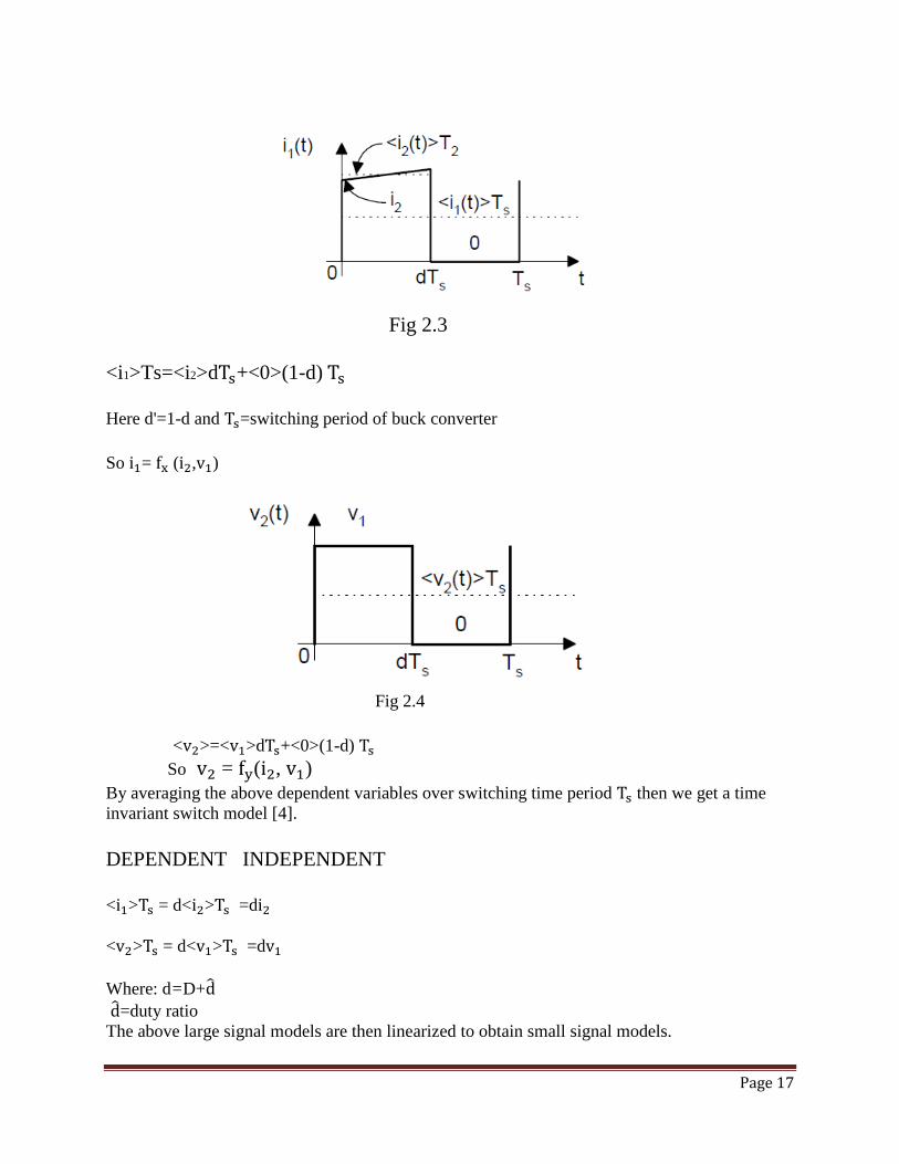
Page 17
Fig 2.3
<i1>Ts=<i2>d +<0>(1-d)
Here d'=1-d and =switching period of buck converter
So = ( , )
Fig 2.4
< >=< >d +<0>(1-d)
So = ( , )
By averaging the above dependent variables over switching time period then we get a time
invariant switch model [4].
DEPENDENT INDEPENDENT
< > = d< > =d
< > = d< > =d
Where: d=D+
=duty ratio
The above large signal models are then linearized to obtain small signal models.
Page 18
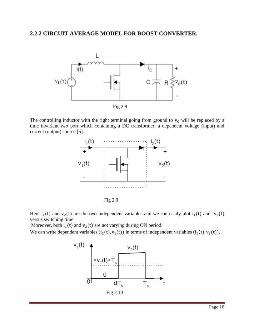
2.2.2 CIRCUIT AVERAGE MODEL FOR BOOST CONVERTER.
Fig 2.8
The controlling inductor with the right terminal going from ground to will be replaced by a
time invariant two port which containing a DC transformer, a dependent voltage (input) and
current (output) source [5].
Fig 2.9
Here and are the two independent variables and we can easily plot and
versus switching time.
Moreover, both and are not varying during ON period.
We can write dependent variables ( in terms of independent variables ( .
Fig 2.10

Page 19
= ( , )
Then averaging the dependent variable over switching period .
< d'< (t)> =d'
Where d‘=1-d
Fig 2.11
= ( , )
Then averaging the dependent variable over switching period in terms of independent
variable.
< =<0> =
Fig 2.12
Page 20
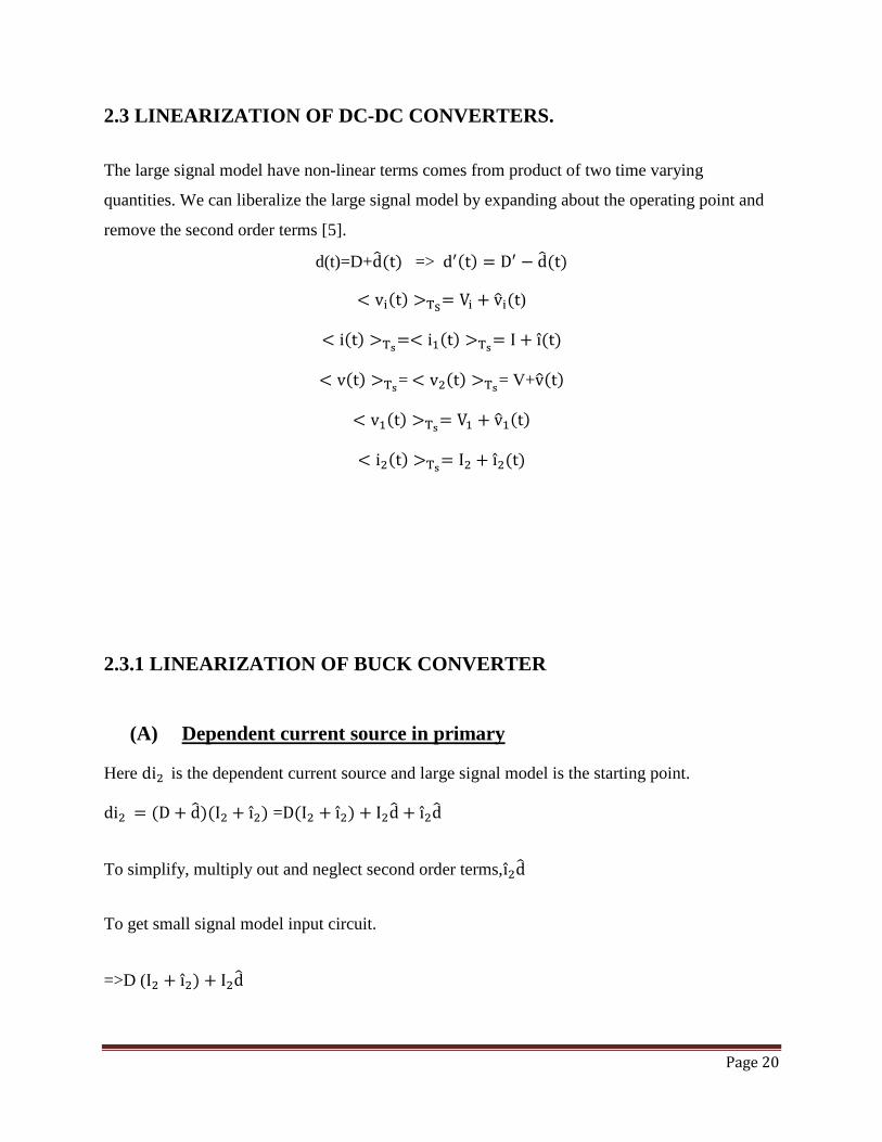
2.3 LINEARIZATION OF DC-DC CONVERTERS.
The large signal model have non-linear terms comes from product of two time varying
quantities. We can liberalize the large signal model by expanding about the operating point and
remove the second order terms [5].
d(t)=D+ =>
)
=
= V+
2.3.1 LINEARIZATION OF BUCK CONVERTER
(A) Dependent current source in primary
Here is the dependent current source and large signal model is the starting point.
=
To simplify, multiply out and neglect second order terms,
To get small signal model input circuit.
=>D (

Page 21
RESULT
Fig 2.5
(B) Dependent voltage source in secondary
Here is the dependent voltage source
= (D+ ) ( )
=D ( ) + +
To simplify, multiply out and neglect second order terms to
Get small signal output model.
=D( ) +
RESULT
Fig 2.6

Page 22
(C) Combine small signal I/O circuits via ac/DC transformer. The dependent DC sources are replaced by an equivalent ideal DC transformer with turns ratio
1:D. This gives final DC and small signal AC circuit averaged model [5], [3].
Fig 2.7 For a DC model only, assume 0 and we get the old DC Buck converter model.
2.3.2 LINEARIZATION OF BOOST CONVERTER
(A) Dependent voltage source in primary side.
Here d'=D'-
< =d'< (t)> =d' =(D'- )( )
( )
Multiply out the product terms and neglect second order
Terms in the input circuit. The result is the new input circuit model:
( )

Page 23
RESULT
Fig 2.13
(B) Dependent current source in secondary
< =<0> =
- )( + )
To simplify, multiply out and neglect second order terms in the output circuit.
- )( + )=
=> ( )
Fig 2.14
(C) Combine the small signal I/O circuits via DC/ac transformer
The dependent sources are replaced by an equivalent ideal DC transformer with turns ratio .
This gives the final DC and small-signal ac circuit-averaged model for boost converter.

Page 24
Fig 2.15
For DC model only, let 0 and we get the old DC boost converter model.

Page 25
CHAPTER 3
SMALL SIGNAL MODELING OF PCM-CONTROLLED DC-DC
BUCK CONVERTER
3.1 peak current mode control for buck converter.
3.2 Derivation of current loop transfer function.
3.2.1 Derivation without input filter (without and )
3.2.2 Derivation with input filter (without and )
3.2.3 Derivation without input filter (with and )
3.2.4 Derivation with input filter (with and )
Page 26
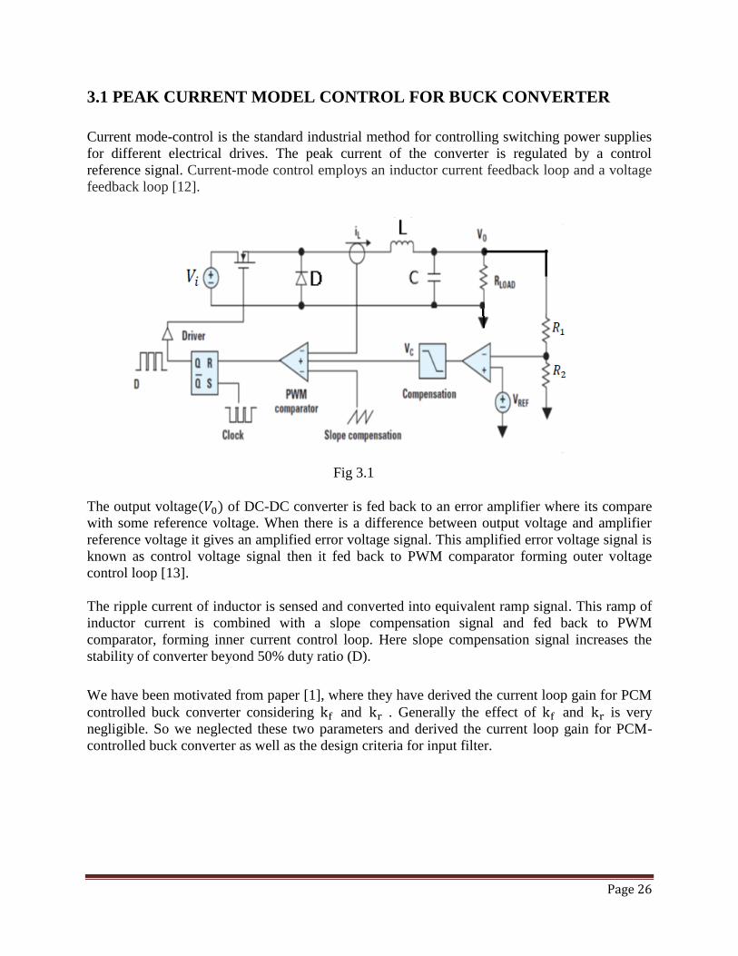
3.1 PEAK CURRENT MODEL CONTROL FOR BUCK CONVERTER
Current mode-control is the standard industrial method for controlling switching power supplies
for different electrical drives. The peak current of the converter is regulated by a control
reference signal. Current-mode control employs an inductor current feedback loop and a voltage
feedback loop [12].
Fig 3.1
The output voltage of DC-DC converter is fed back to an error amplifier where its compare
with some reference voltage. When there is a difference between output voltage and amplifier
reference voltage it gives an amplified error voltage signal. This amplified error voltage signal is
known as control voltage signal then it fed back to PWM comparator forming outer voltage
control loop [13].
The ripple current of inductor is sensed and converted into equivalent ramp signal. This ramp of
inductor current is combined with a slope compensation signal and fed back to PWM
comparator, forming inner current control loop. Here slope compensation signal increases the
stability of converter beyond 50% duty ratio (D).
We have been motivated from paper [1], where they have derived the current loop gain for PCM
controlled buck converter considering and . Generally the effect of and is very
negligible. So we neglected these two parameters and derived the current loop gain for PCM-
controlled buck converter as well as the design criteria for input filter.

Page 27
3.2 DERIVATION OF CURRENT LOOP TRANSFER FUNCTION.
PCM-controlled buck converter with an input filter
Fig 3.2 SMALL SIGNAL MODEL OF PCM-CONTROLLED BUCK CONVERTER
WITH AN INPUT FILTER
Fig 3.3

Page 28
3.2.1 DERIVATION WITHOUT INPUT FILTER (without and )
Without input filter impedance , the dependent current source is shorted and the inductor
current is representing as:
( )
Where;
(
)
(
*
Fig 3.3
Here =1
Now current loop gain given by;
3.2.2 DERIVATION WITH INPUT FILTER (without and )
When input filter is considered, the terminal voltage of in figure can be expressed as below,
( )
Applying KVL

Page 29
Substituting equation (5) in (6) and rearranging we get,
(
*
Again we know,
Putting equation (8) in (7) we get,
(
*
(
)
Can be written as,
Now from eq.(9) and (10) we can draw the block diagram with modified current loop gain

Page 30
Fig 3.4
Thus modified current loop gain is given by;
(
,
3.2.3 DERIVATION WITHOUT INPUT FILTER (with and )
Without input filter impedance , the dependent current source should be shorted derectly.
Now;
Its corresponding secondary voltage is
Thus current is given by;
Where;

Page 31
(
*
Now the duty ratio is given by
From equation (14) and (16) we can draw the block diagram;
Fig 3.5
From the block diagram, the current loop gain is given by;
3.2.4 DERIVATION WITH INPUT FILTER (with and )
When input filter is considered the terminal voltage of will appear and is given by;
( )
Applying KVL, we get;
Substituting equation (16) in (17) we get;
( )
(
*

Page 32
Now the corresponding secondary voltage of is
Now the current is given by;
Putting eq.(19) in (18) we get,
(
*
(
)
( )
Now multiplied by equation (16), we get;
( )
From the figure duty ratio will be given by;
Putting equation (21) in (22), the duty ratio will be
( ( ) )

Page 33
From equation (20) and (23) we can draw the block diagram;
Fig 3.6
Now the modified current loop gain will be given by;
(
,

Page 34
CHAPTER 4
BASIC DESIGN CRITERIA FOR INPUT FILTER
4.1 Basic design criteria for input filter
4.2 Input filter parameters for buck converter

Page 35
4.1 BASIC DESIGN CRITERIA FOR INPUT FILTER
(Considering )
Current loop gain from equation (15) without input filter is given by;
=
Current loop gain from eq (24) with inputfilter is given by;
(
*(
)
If sampling effect is not taken into consideration ( =1)
Now using eq(15) in eq(24), modified current loop gain( ) will be
(
*(
)
(
,(
)
Now putting
(where is equivalent admittance of input filter)
(
)(
+ (s)
(
) (
) (s) (25)
Where
=

Page 36
Where =slope of external ramp , =slope of control ramp during on time
If the modified current loop gain is approximately equal to unmodified current loop gain
i.e (s)
following fours conditions are obtained;
|
| (26)
|
|
|
|
|
|
As the effect of on converter is very less as they are very small, they can be neglected
Current loop gain from equation (4) without input filter is given by;
=
Current loop gain from equation(11)with inputfilter is given by;
(
)
Now using eq(4) in eq(11), modified current loop gain( ) will be
(
)
(
,

Page 37
Where (31)
(32)
(33)
If the modified current loop gain is approximately equal to unmodified current loop gain.
i.e (s)
following two conditions will be satisfied
|
|
|
|
If inequality (34) not satisfied it will lead to oscillate and if inequality (35) is not satisfied
converter dynamic performance will be degraded.
4.2 INPUT FILTER PARAMETERS FOR BUCK CONVERTER
Fig 4.1
The equivalent circuit between point A and B excluding is shown below;

Page 38
Fig 4.2
Now equivalent impedence( ) between point A and B given by;
Multiplying
) both in neumerator and denominator ,we get;
(
)
[
] * (
)
+
+
+
-
(36)
Above equation can be written as;
Where
(37)

Page 39
When frequency(w) is close to resonant frequency of inputfilter, it will have minimum
admittance.
i.e
(38)
Where ;
Putting w =
√
The input filter of PCM controlled buck converter remains stable as long as satisfy the
inequalities (34), (35). From equation (39) is directly proportional to
. If
is
large, will increase and not satisfy inequalities (34), (35) causing the converter to
oscillate. So
should not be very large [1].
Page 40
CHAPTER 5
MATLAB SIMULATION
5.1 Buck converter circuit parameters(R, L, and C)
5.2 Calculation of admittance
5.3 Simulink model for PCM-controlled buck converter without input filter
5.4 Simulink model for PCM-controlled buck converter with input filter
5.5 Simulink model for PCM-controlled buck converter with input filter (instability)

Page 41
5.1 BUCK CONVERTER CIRCUIT PARAMETERS(R, L, C)
Fig 4.3
Let‘s assume;
Input voltage ( ) =12 volt
Output voltage ( ) =4.8 volt
Load current ( ) =3 ampere
As we know;
…………. (1) Where D is duty ratio,
Given by D=
)
Putting the values in eq(1)
D =
=
=0.4
Let us assume switching frequency ( ) =100K
R=
= 1.6
Taking inductor current ripple ( ) equal to 30% of
Thus = 0.9 amp
Taking capacitor voltage ripple ( ) equal to 0.4% of
Thus = 0.0192 volt

Page 42
CALCULATION OF VALUE OF INDUCTOR
Current ripple factor is given by;
=
(where is switching period)
CALCULATION OF VALUE OF CAPACITOR
Voltage ripple factor is given by;
Assuming the Values of
5.2 CALCULATION OFADMITTANCE :-
Here given data are D=0.4,R=1.6 ,L=32 ,C=58.59 ,
From equation (32)
| |
As we know from equation (31)
Where

Page 43
Putting the value of L, C, R, in above equation
Thus
Putting the value of ‗Y‘ in equation (31)
Magnitude of is given by | |
From equation (38) we know | |
The values of| |, | |, | | satisfies the inequalities(34), (35) and converter is stable and wave
forms are shown in fig.5.6
When the value of is larger than
Let and
| |
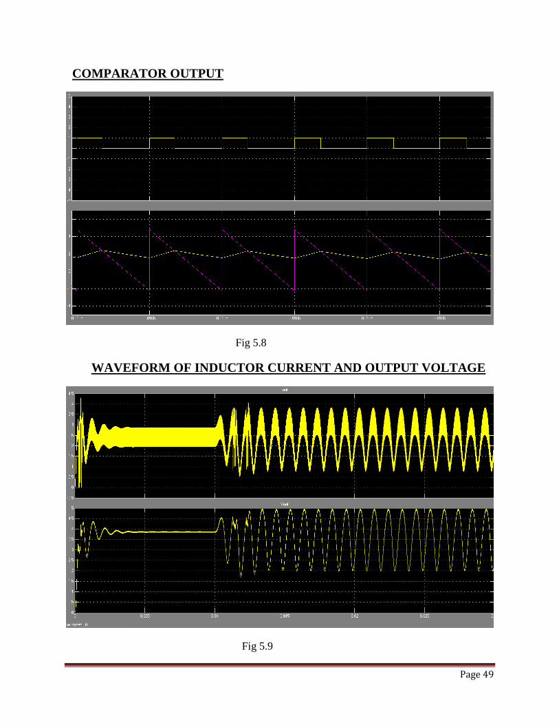
Which does not satisfy the inequalities (34), (35) and converter oscillate. Wave forms are shown
in fig.5.9

Page 44
5.3 SIMULINK MODEL FOR PCM-CONTROLLED BUCK
CONVERTER WITHOUT INPUT FILTER
Fig 5.1

Page 45
COMPARATOR OUTPUT (GATE PULSE)
Fig 5.2
WAVEFORM OF INDUCTOR CURRENT AND OUTPUT VOLTAGE
Fig 5.3

Page 46
5.3 SIMULINK MODEL FOR PCM-CONTROLLED BUCK CONVERTER
WITH INPUT FILTER
Fig 5.4

Page 47
COMPARATOR OUTPUT (GATE PULSE)
Fig 5.5
WAVEFORM OF INDUCTOR CURRENT AND OUTPUT VOLTAGE
Fig 5.6
Page 48
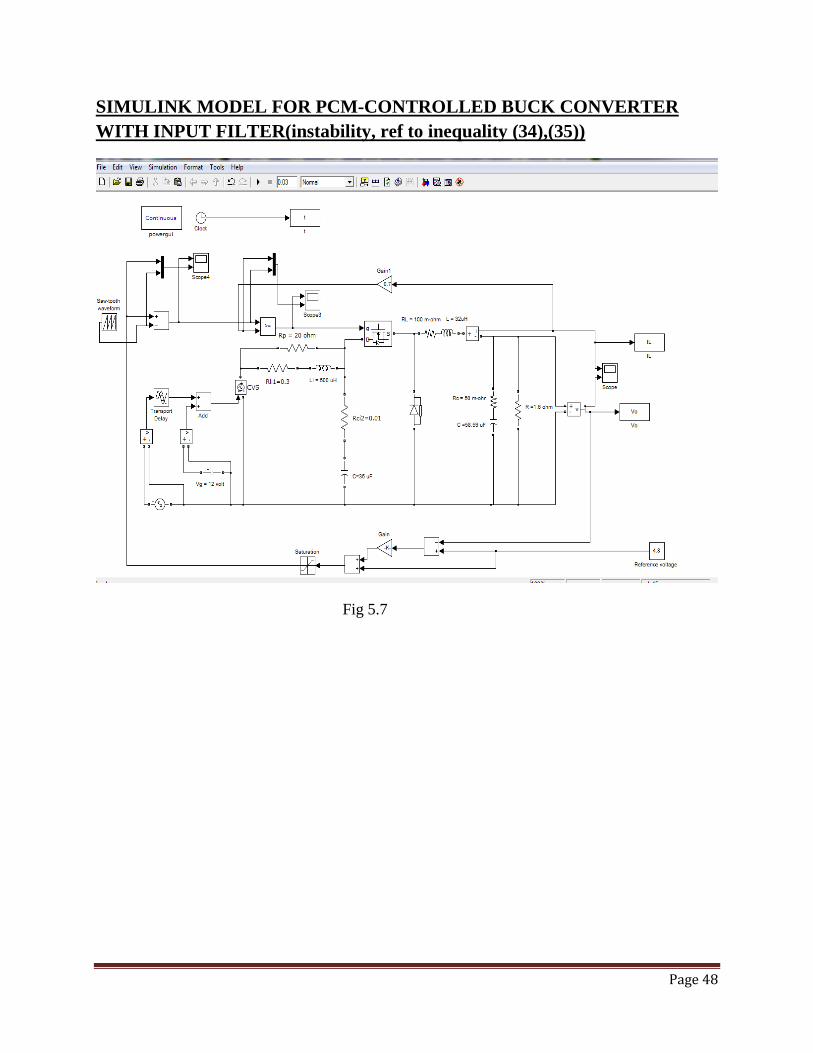
SIMULINK MODEL FOR PCM-CONTROLLED BUCK CONVERTER
WITH INPUT FILTER(instability, ref to inequality (34),(35))
Fig 5.7
Page 49
COMPARATOR OUTPUT
Fig 5.8
WAVEFORM OF INDUCTOR CURRENT AND OUTPUT VOLTAGE
Fig 5.9
Page 50
CHAPTER 6
6.1 CONCLUSION
6.2 REFERENCES
Page 51
6.1 CONCLUSION
DC-DC converters are used in many applications, such as battery charger,
computer and electrical drives in industry for controlling the DC voltage. However
electromagnetic interference present in power signal affects the performance of
DC-DC converter. So generally an input filter is added to converter to reduce the
electromagnetic interference. Here effect of input filter in current controlled DC-
DC buck converter is studied. The design criteria for input filter without
considering and are derived. Output of buck converter with and without input
filter is examined in stable and unstable condition of PCM controlled buck
converter using MATLAB. It reduces the EMI significantly.

Page 52
6.2 REFERENCES
[1] Shen-Yaur chen and Jin-Jia Chen, ―study of the effect and design criteria of the input filter
for buck converters with peak current-mode control using a novel system block diagram,‖ IEEE
transactions on industrial electronics, vol.55, No.8, august 2008.
[2] R.W. Erickson and D Maksimovi, ―Fundamentals of Power Electronics, second edition.‖
Kluwer Academic Publishers, 2001.
[3] Vatche Vorperian, ―simplified analysis of PWM converters using model of PWM switch part
I: continuous conduction mode,‖ IEEE transactions on aerospace and electronic systems, vol.26,
no.3, may 1990.
[4] jingquan chen, robort Erickson, and dragan maksimovic, ―IECON‘01: the 27th
annual
conference of the IEEE industrial electronics society‖2001.
[5] www.engr.colostate.edu/ECE562/98 lectures/142.pdf
[6] C. R. Kohut, ―Input filter design criteria for switching regulators using Current-mode
programming,‖ IEEE transactions on Power Electronics., vol. 7, no. 3,pp. 469–479, Jul. 1992.
[7] S. Y. Erich and W. M. Polivka, ―Input filter design criteria for current programmed
Regulators,‖ IEEE Transactions on Power Electronics, vol. 7, no. 1,pp. 781–791, Jan. 1992.
[8] B. Choi, D. Kim, D. Lee, S. Choi, and J. Sun, ―Analysis of input filter Interactions in
switching power converters,‖ IEEE Transactions on Power Electronics,vol. 22, no. 2, pp. 452–
460, Mar. 2007.
[9] R. B. Ridley, a New Small-Signal Model for Current-Mode Control.Roswell, GA: Ridley
Eng., Inc., 1999.
[10] R.B. Ridley, ―A New Small-Signal Model for Current-Mode Control‖, PhD Dissertation,
Virginia Polytechnic Institute and State University, November, 1990.
[11] V. Vorpérian, ―Analysis of Current-Mode Controlled PWM Converters Using the Model of
the Current-Controlled PWM Switch.‖ Power Conversion and Intelligent Motion, October 1990.
[12] http://encon.fke.utm.my/nikd/latest/jul_01_designer.pdf

Page 53
[13] www.national.com/vcm/national3/en_US/resources/power_designer/powerdesigner_106.pdf
[14] S. Wang, J. D. van Wyk, and F.C. Lee, ―Effects of interactions between filter parasitic and
power interconnects on EMI filter performance,‖ IEEE transactions on Industrial Electronics,
vol.54, no.6, pp.3344-3352, Dec. 2007
[15] R. D. Middle brook, ―Modeling a current-programmed buck regulator,‖ in
Proc. IEEE Application Power Electronics, Conf., Rec., 1987, pp. 3–13.
[16] Patrick L. Chapman, Senior Member, IEEE―Numerical Dynamic Characterization of Peak
Current-Mode-Controlled DC–DC Converters‖ IEEE TRANSACTIONS ON CIRCUITS AND
SYSTEMS—II: EXPRESS BRIEFS, VOL. 56, NO. 12, DECEMBER 2009.
[17]Edwin van Dijk, Herman J. N. Spruijt, Dermot M. O‘Sullivan, and J. Ben Klaassens ―PWM-
Switch Modeling of DC-DC Converters‖IEEE TRANSACTIONS ON POWER
ELECTRONICS, VOL. 10, NO. 6, NOVEMBER 1995