sub-22 nm line and space patterning using resist reflow ... workshop/oral 47 resist-2 cho.pdf ·...
TRANSCRIPT

Sub-22 nm Line and Space Patterning using Resist Reflow Process
for Extreme Ultra-Violet Lithography
In Wook Cho*, Hyunsu Kim, Jee-Hye You, Hye-keun Oh
Department of Applied Physics, Hanyang University, S. Korea
2009 International Workshop On EUV Lithography (RESIST-2), Hawaii
2009. 7. 16

2009 International Workshop On EUV Lithography
Contents
Introduction
Simulation Results– Simulation Conditions– Simulation Window
• Monte-Carlo System• Resist Reflow Process
– Simulation Results
Summary

2009 International Workshop On EUV Lithography
Introduction
http://www.itrs.net/Links/2007ITRS/2007_Chapters/2007_Lithography.pdf

2009 International Workshop On EUV Lithography
Motivation
LER reduction by RRP.
Before RRP
LER ~ 6 nm LER ~ 2 nm
After RRP

2009 International Workshop On EUV Lithography
Resist Reflow Process (RRP)
Resist Reflow Process(RRP) is a simple technique that the resist is bakedat above its glass transition temperature (Tg) after the development process.
Strength : No need for extra Chemicals/ Simple ProcessWeakness : High pitch dependency / Round top profiles after shrink
/ High resist dependency / High shrink rate (~ 5 nm/ )
After RRP

2009 International Workshop On EUV Lithography
Resist Reflow Process Mechanism
Initial structure /arbitrary process condition
Boundary movement
Fluid flow
Surface tension
Viscosity TemperatureCurve fitting
Navier-Stokes eq.
Output
Temperature,contact angle
Bulk effect & adhesion effect
TemperatureDeveloped patternPitchTime
Input Parameters
CD after reflowResist top / side view
Output

2009 International Workshop On EUV Lithography
Exposure• Aerial Image(from Solid-EUV)
• Dose
Post Exposure Bake• Time• Temperature
Development• Time• Model
Monte-Carlo System
Input Parameters
Post Exposure Bake
Development
Developed Resist ProfileOutput
Hyunsu Kim, et, al., “Line Width Roughness Investigation through Resist Molecular Structure in Extreme Ultra-violet Lithography” (Resist-3), EUVL 2009, Poster Session. “[email protected]”
More Details :
Exposure Process

2009 International Workshop On EUV Lithography
Simulation Condition
1:3 (11 nm : 33 nm) Line & Space Aerial Image from Solid-EUV is intentionallymade to make 1:1 (22:22 nm) L/S.
Dose PEB time PEBtemperature Develop time RRP time RRP
temperature10.1 mJ/cm2 60 s 120 60 s 0 ~ 100 s 138 ~ 142
2009 International Workshop On EUV Lithography
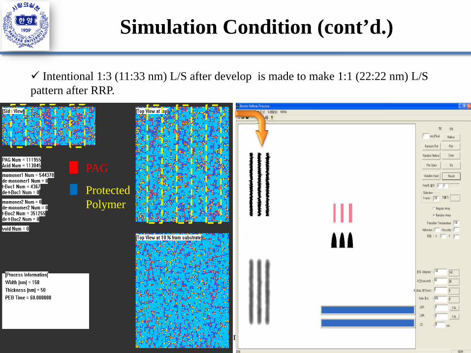
Simulation Condition (cont’d.)
Intentional 1:3 (11:33 nm) L/S after develop is made to make 1:1 (22:22 nm) L/S pattern after RRP.
PAG
ProtectedPolymer

2009 International Workshop On EUV Lithography
Line Edge Roughness
Post Development Bake: T< Tg (PDB) vs. T>Tg (RRP)
After RRP, LER is reduced from 7 nm down to 2 nm, while after PDB, LER is reduced from 7.5 nm to ~ 5 nm only.
As temperature goes high and time passes by, LER decreases.
<After PDB> <After RRP>

2009 International Workshop On EUV Lithography
Line Width Roughness
• When RRP is applied, the LWR is shrunken from 6 to ~ 2 nm.• At 142 , shrinkage decreases more rapidly than at 136 because Tg is 136 .• RRP can be used to reduce the surface roughness below 2 nm.
Post Development Bake: T< Tg (PDB) vs. T>Tg (RRP)
<After PDB> <After RRP>

2009 International Workshop On EUV Lithography
Effect of RRP Temperature
• LER and LWR decreases as RRP temperature increases.• Around Tg, the decrement of LER and LWR after bake is smaller compared to highertemperature RRP.

2009 International Workshop On EUV Lithography
LER and LWR decrease with RRP time.
1 2 3

2009 International Workshop On EUV Lithography
Surface roughness reduction & CD increase
After RRP35 s,
142 ℃
Top View
Side View
Top View
Side View

2009 International Workshop On EUV Lithography
CD increase with RRP time (142, 140, 138 ℃)
As RRP time goes by, resist flows more, and the resist linewidth increases.
1 2 3

2009 International Workshop On EUV Lithography
Optimum RRP time with 142 ℃
CD ± 10 %

2009 International Workshop On EUV Lithography
Summary
Resist Reflow Process is suggested to reduce LER and LWR without any additional chemical process in EUV lithography.
Using RRP, we could obtain smaller LER and LWR, ~2 nm.
As RRP time goes by and RRP temperature is higher, LER and LWR decrease, but the linewidth becomes wider.
We could obtain 1:1 22 nm L/S pattern with intentional 1:3 (11:33) L/S pattern and proper RRP condition.

2009 International Workshop On EUV Lithography
Thank you for your attention!!