sub-nanometer attening of a 45-cm long, 45-actuator x-ray ... · attening of a 45-cm long,...
TRANSCRIPT

Sub-nanometer flattening of a 45-cm long, 45-actuator x-raydeformable mirror
Lisa A. Poyneer,1, ∗ Thomas McCarville,1 Tommaso Pardini,1 DavidPalmer,1 Audrey Brooks,2 Michael J. Pivovaroff,1 and Bruce Macintosh1
1Lawrence Livermore National Laboratory, 7000 East Avenue, Livermore, California 94550, USA2Northrop Grumman, AOA Xinetics Inc., 115 Jackson Rd, Devens, MA 01434, USA
compiled: April 3, 2018
We have built a 45-cm long x-ray deformable mirror of super-polished single-crystal silicon that has 45actuators along the tangential axis. After assembly the surface height error was 19 nm rms. With useof high-precision visible-light metrology and precise control algorithms, we have actuated the x-raydeformable mirror and flattened its entire surface to 0.7 nm rms controllable figure error. This is, toour knowledge, the first sub-nanometer active flattening of a substrate longer than 15 cm.
OCIS codes: 220.1080, 340.7470, 120.4640, 230.4040
http://dx.doi.org/10.1364/XX.99.099999
1. IntroductionThe advent of 4th-generation x-ray light sources(i.e., free electron lasers like the Linac CoherentLight Source in the U.S. and SPring-8 AngstromCompact free electron laser in Japan and advancedsynchrotrons like the National Synchrotron LightSource II in the U.S.) requires increasingly ad-vanced and high-performance x-ray mirrors. Com-bining expertise in visible wavelength adaptive op-tics and reflective x-ray optics, Lawrence LivermoreNational Laboratory (LLNL) has begun a researchand development effort to design, fabricate and testx-ray deformable mirrors.
X-ray deformable mirrors could provide two sig-nificant benefits over traditional non-adaptive x-rayoptics. First, active control is a potentially inex-pensive way to achieve better surface figure thanis possible by polishing alone, particularly on longsubstrates. Secondly, the ability to change the fig-ure allows for dynamic correction of aberrations in ax-ray beam line. This includes both self-correctionof errors in the mirror itself (such as those caused bythermal loading) and correction of errors on otheroptics, the latter of which has been demonstratedelsewhere[1].
With these goals in mind we have built a 45-cm
∗ Corresponding author: [email protected]
x-ray deformable mirror (XDM). As detailed below,this mirror was designed to provide fine-scale con-trol of its surface. Using precise visible-wavelengthmetrology, we have been able to generate voltagecommands for the XDM’s actuators that flatten itto as good as 0.7 nm rms, which is significantlybetter than the initial substrate polishing before as-sembly. The following sections describe the XDM,the metrology equipment, our calibration and con-trol methods and finally the flattening results.
To place our XDM in context, we must considertwo types of mirrors that have been developed byothers in the field. The first is with non-activesuper-polished mirrors. We need to be able tocontrol our XDM to a comparable flatness. OurXDM was designed with the same size specifica-tions as the hard x-ray offset mirrors (known asHOMS) for LCLS [2, 3]. Visible-light metrology(using the same interferometer that we have usedfor this work) on the four delivered HOMS mea-sured the figure errors (which exclude cylinder) be-tween 1.0 and 2.4 nm rms [2, 3]. JTEC producesmirrors up to 50 cm long, with a claimed shapeerror of less than 0.5 nm rms at best effort [4].
Although fixed figure 0.5 m flats with < 0.5 nmrms error are being produced, the advantages of avariable figure capable 0.5 nm figure error tolerancemotivate this study. For example, a variable figuremirror can compensate for localized heating that
arX
iv:1
402.
1743
v2 [
phys
ics.
ins-
det]
24
Apr
201
4

2
drives figure error well above the as manufacturedspecification. If mirrors are coated, a concomitantcylinder can be compensated. Finally, a deformablemirror may aid in compensating figure errors intro-duced by final focusing optics, which are not yetbeing manufactured to diffraction limited perfor-mance. One deformable mirror can correct the netsum of all these effects, without the need to fullyunderstanding the origin of each component.
The second point of comparison for our XDM isto other deformable x-ray optics. Below, we sum-marize published performance of the best flatten-ing achieved for other deformable x-ray mirrors. In2010 a French collaboration [5] developed an activex-ray mirror to be deployed at the SOLEIL facility;this mirror implements a 35 × 4 × 0.8 cm siliconsubstrate held between an active jaw and a flexor,to generate variable elliptical profiles. In additionthe mirror features 10 actuators across its lengthto minimize asphere. The actuators are perpendic-ular to the mirror surface, and force is applied bya spring-floating head coupled to a stepper motor.Actuator hysteresis was reported to be 0.1%. TheSOLEIL team demonstrated flattening of the mir-ror down to 3.0 nm rms of asphere, and 0.6µradslope errors over 30 cm of clear aperture, with amaximum radius of curvature equal to 60 m.
In the same year, the Diamond Light Source de-veloped a 15 × 4.5 cm adaptive x-ray mirror, in-cluding eight piezo bimorph actuators [6]. Thismirror was specifically designed to achieve a highlevel of figure control, while allowing for adjustableradius of curvature. The actuated mirror, built bySESO and super polished by JTECH via ElasticEmission Machining (EEM), reached 0.66 nm rmsof asphere over 12 cm of clear aperture, with thesmallest beam size at focus equal to 1.2 µm FWHM.
Another x-ray deformable mirror was developedin Japan and deployed at SPring-8 before a pair ofKirkpatrick-Baez (KB) mirrors, to achieve nearlydiffraction-limited beam focusing [7]. The 12 cmsilicon substrate was super-polished by EEM, andfeatures 16 piezoelectric plates. During operation,a Fizeau interferometer was placed in front of themirror to provide real time figure correction. Theexperimental team reported a 7 nm FWHM spotsize at the focus plane. For this experiment an es-timated 10 nm peak-to-valley surface profile wasfound in situ, but several error sources were listed.Previously, visible light metrology on this optic [8]outside of the beam line was conducted with Fizeauinterferometry. An approximately 2 nm peak-to-valley figure error was measured at best flat. No
rms figure error was reported; for a typical figureerror PSD this is approximately 0.7 nm rms.
In 2012 the x-ray optic group at the Elettra Syn-chrotron facility in Italy reported on the success-ful construction of an adaptive x-ray mirror for theTIMEX beamline at FERMI [9]. This mirror is 40cm long and 4 cm wide, and features 13 piezo ac-tuators and 13 strain gauges. Rough flattening ofthe mirror is first achieved by acting on four clampslocated on the mirror mount. The idea of includ-ing calibrated strain gauges in the design allows themirror to work in closed loop without the need of awavefront sensor. The same idea was implementedfor the design of our XDM. To our knowledge noprecision flattening results have been reported fromElettra.
2. Deformable mirror design
Our single crystal silicon substrate is 45 cm inlength, 3 cm high, and 4 cm in width. Substratequality is discussed in Section 4. The mirror andactuators are supported on an invar mount, andenclosed in a protective housing that leaves the re-flective surface exposed to grazing incidence x-rays.The substrate was cut from a large boule similarto those typically used in wafer fabrication, whichare usually pulled in the (111) direction. Typicalresistivity is < 10 ohm-cm. Neither parameter hasany significant affect on our mirror’s performance.As of now we do not expect to deposit any singleor multilayer coating on the silicon substrate. Pre-liminary experiments at a synchrotron facility willbe conducted at low photon energy and grazing in-cidence, well within the critical angle of silicon.
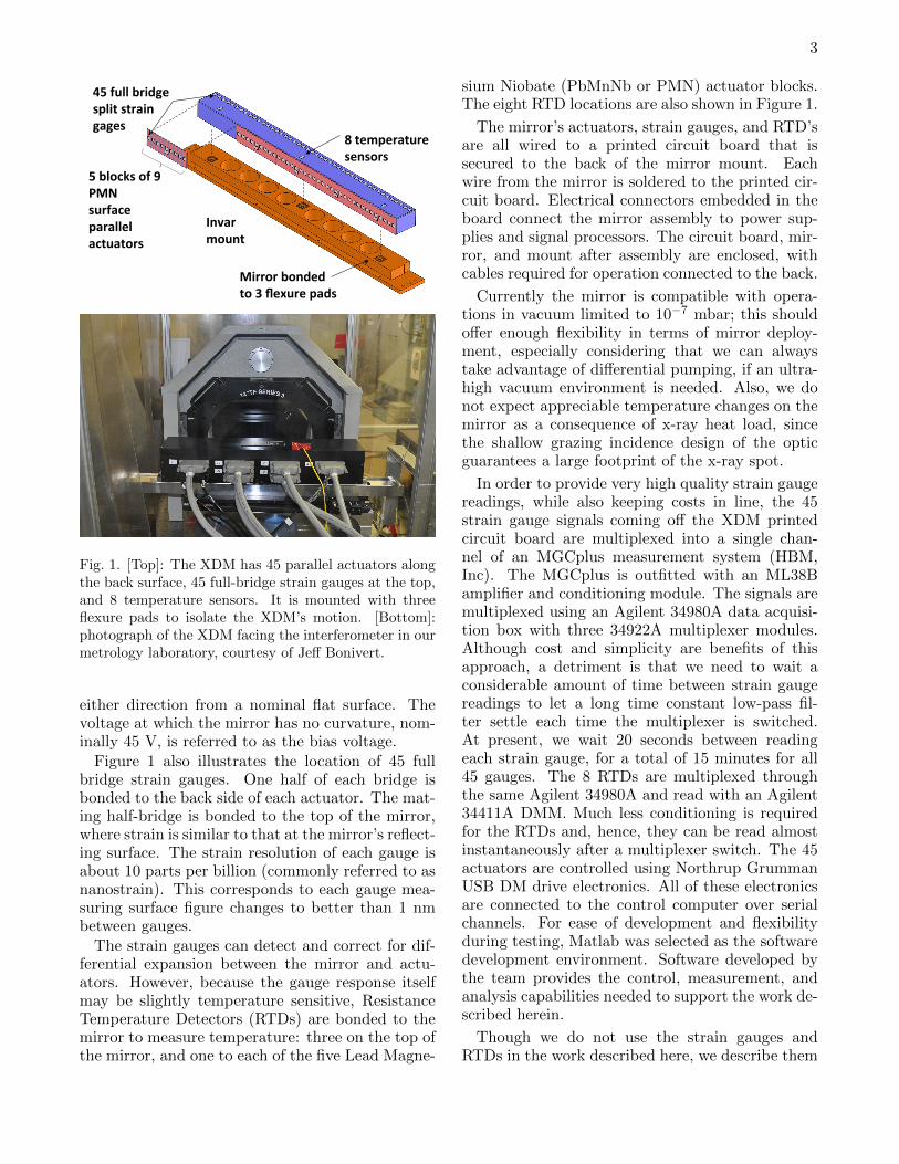
Figure 1 illustrates how the 45 actuators arebonded on the side opposite the reflective surface.Each actuator is 1 cm long, 3 cm high, and about0.15 cm thick. They are spaced evenly every 1 cmalong the tangential axis of the mirror. The surfaceparallel actuator geometry of the actuators, alongwith three flexure supports machined into the Invarmount, minimize unintended forces on the mirror,and their effect on figure during actuation. Theactuators are epoxy bonded to the mirror while atmid-range of their operating voltage, which enablesthe mirror to bend both concave and convex. Themirror is bonded to the three flexure pads to con-strain all motion except that induced by the actu-ators. The flexures also isolate the mirror from dif-ferential thermal expansion between the substrateand mount.
The actuators operate from 15 to 75 volts. Theactuators were bonded to the substrate at 45 V.This enables the XDM to make spherical surface in
3
5"blocks"of"9"PMN"surface"parallel"actuators"
45"full"bridge"split"strain"gages"
Mirror"bonded"to"3"flexure"pads"
8"temperature"sensors"
Invar"mount"
Fig. 1. [Top]: The XDM has 45 parallel actuators alongthe back surface, 45 full-bridge strain gauges at the top,and 8 temperature sensors. It is mounted with threeflexure pads to isolate the XDM’s motion. [Bottom]:photograph of the XDM facing the interferometer in ourmetrology laboratory, courtesy of Jeff Bonivert.
either direction from a nominal flat surface. Thevoltage at which the mirror has no curvature, nom-inally 45 V, is referred to as the bias voltage.
Figure 1 also illustrates the location of 45 fullbridge strain gauges. One half of each bridge isbonded to the back side of each actuator. The mat-ing half-bridge is bonded to the top of the mirror,where strain is similar to that at the mirror’s reflect-ing surface. The strain resolution of each gauge isabout 10 parts per billion (commonly referred to asnanostrain). This corresponds to each gauge mea-suring surface figure changes to better than 1 nmbetween gauges.
The strain gauges can detect and correct for dif-ferential expansion between the mirror and actu-ators. However, because the gauge response itselfmay be slightly temperature sensitive, ResistanceTemperature Detectors (RTDs) are bonded to themirror to measure temperature: three on the top ofthe mirror, and one to each of the five Lead Magne-
sium Niobate (PbMnNb or PMN) actuator blocks.The eight RTD locations are also shown in Figure 1.
The mirror’s actuators, strain gauges, and RTD’sare all wired to a printed circuit board that issecured to the back of the mirror mount. Eachwire from the mirror is soldered to the printed cir-cuit board. Electrical connectors embedded in theboard connect the mirror assembly to power sup-plies and signal processors. The circuit board, mir-ror, and mount after assembly are enclosed, withcables required for operation connected to the back.
Currently the mirror is compatible with opera-tions in vacuum limited to 10−7 mbar; this shouldoffer enough flexibility in terms of mirror deploy-ment, especially considering that we can alwaystake advantage of differential pumping, if an ultra-high vacuum environment is needed. Also, we donot expect appreciable temperature changes on themirror as a consequence of x-ray heat load, sincethe shallow grazing incidence design of the opticguarantees a large footprint of the x-ray spot.
In order to provide very high quality strain gaugereadings, while also keeping costs in line, the 45strain gauge signals coming off the XDM printedcircuit board are multiplexed into a single chan-nel of an MGCplus measurement system (HBM,Inc). The MGCplus is outfitted with an ML38Bamplifier and conditioning module. The signals aremultiplexed using an Agilent 34980A data acquisi-tion box with three 34922A multiplexer modules.Although cost and simplicity are benefits of thisapproach, a detriment is that we need to wait aconsiderable amount of time between strain gaugereadings to let a long time constant low-pass fil-ter settle each time the multiplexer is switched.At present, we wait 20 seconds between readingeach strain gauge, for a total of 15 minutes for all45 gauges. The 8 RTDs are multiplexed throughthe same Agilent 34980A and read with an Agilent34411A DMM. Much less conditioning is requiredfor the RTDs and, hence, they can be read almostinstantaneously after a multiplexer switch. The 45actuators are controlled using Northrup GrummanUSB DM drive electronics. All of these electronicsare connected to the control computer over serialchannels. For ease of development and flexibilityduring testing, Matlab was selected as the softwaredevelopment environment. Software developed bythe team provides the control, measurement, andanalysis capabilities needed to support the work de-scribed herein.
Though we do not use the strain gauges andRTDs in the work described here, we describe them

4
for completeness. These sensors were included tohelp us control the XDM’s stability through timeand with temperature changes, which is a subjectfor future work. We next discuss the visible lightmetrology that we use to characterize the XDM.
3. Visible-light metrology3.A. The 12-inch Zygo interferometerThe Zygo Mark II phasing interferometer used inthis work has a noise floor of about 0.3 nm, and iscalibrated to measure figure with an absolute accu-racy approaching 1 nm (rms) over the 28 cm fieldof view. The 45 cm deformable mirror figure isconstructed by stitching three 28 cm long interfero-grams. Without suitable characterization, interfer-ometer calibration errors will produce inconsisten-cies within stitched regions, limiting the ability todemonstrate deformable mirror performance.
Therefore a three flat test was used to calibratethe interferometer. During the test two transmis-sion flats, T1 and T2, are mounted onto the inter-ferometer, and also placed at the optic under testlocation. The third optic is a reflection flat labeledR. It is placed at the optic under test location, andis rotatable 180 degrees about its optic axis. Thefigure of each optic along a horizontal line can becalculated from the three data files, and the solu-tion for T2 is used as the reference calibration whenmeasuring our XDM. This reference calibration isshown in Figure 2. This amplitude of the correc-tion is ±5 nm, significantly more than the signalthat we want to measure at best flat.
This study required over a hundred surface figuremeasurements per day during the course of algo-rithm optimization. This measurement rate wouldbest be met with a full aperture visible light in-terferometer. However, the 600 mm aperture in-terferometers tested had a measurement noise floorwell above the 0.1 nm noise floor of our best per-forming 300 mm aperture unit. Off-normal inci-dence angles with additional reflectors were testedusing the 300 mm unit, but the additional air pathlength severely increased the intrinsic instrumentnoise. As a result, the 300 mm unit at normalincidence was selected, and stitching employed tomeasure the full aperture. The performance of thismethod in measuring 450 mm mirrors compared fa-vorably with long trace profile measurements madeat LBL [10], as well as in-situ measurement madeat x-ray wavelengths at LCLS [11].
3.B. Mounting and measuring the XDMAs noted above, we take three measurements of theXDM surface and stitch them together. The mir-
0 0.05 0.1 0.15 0.2 0.25−5
0
5
Position (m) in field of view
Rel
ativ
e he
ight
(nm
)
Reference calibration from three−flat test
Fig. 2. The reference calibration for the interferom-eter, as determined by three-flat test. This shape issubtracted from raw measurements to convert relativeheight to absolute height.
ror’s three positions in front of the interferometerare termed right, center and left. The right posi-tion corresponds to the lowest numbered actuatorson the XDM. The center position is approximatelycentered on actuator 23. The left position corre-sponds to the higher numbered actuators on theXDM. This three-measurement setup provides 20cm overlap in the two stitching zones.
The centerline of the XDM is matched to the cal-ibrated horizontal line of the interferometer. Themount is moved from right to center to left withno vertical motion to ensure the interferometer ismeasuring the mirror at the same elevation. Themount is designed with stops to ensure repeatabil-ity of better than 1 mm (which is one pixel in theinterferometer, see below) as it is moved.
Interferometer measurements are mapped to thephysical surface of the XDM by adjusting inter-ferometer magnification to 1 mm of mirror sur-face/pixel. Each measurement is 288 pixels long,corresponding to 28.8 cm on the XDM surface. Wedefine an x-axis along the centerline of the XDM,with x = 0 at actuator 23. In each of the three posi-tions different actuators are bent and measurementsare taken to determine the exact portion of theXDM that the interferometer measures. At present,in the right position the measurement spans -22.2to 6.5 cm along the x axis (as defined above); incenter position it spans -14.1 to 14.6 cm; in leftposition it spans -6.6 to 22.1 cm.

5
Calibration accuracy is essential for stitching in-terferograms. The interferometer calibration file issubtracted from each measurement to yield the ab-solute height of the XDM. Then piston (constantheight) and tilt (linear height) are removed fromeach measurement. Then, ignoring the fifty pixelsat either end of the measurements, we align the re-maining overlap between the right and center mea-surements. This alignment is done by adjusting thetilt and piston on the right measurement to producethe minimum squared error between it and the cen-ter measurement in the overlap region. Then werepeat the procedure to align the left measurementto the center, again minimizing the squared error.The results of such an alignment are shown in Fig-ure 3. The excellent agreement of the three mea-
−0.2 −0.1 0 0.1 0.2−4
−3
−2
−1
0
1
2
3
4
Position (m)
Abso
lute
hei
ght e
rror (
nm)
Stitch, XDM at flat
RightCenterLeft
Fig. 3. Calibrated interferometer measurements stitchvery well. Three measurements were taken at the samevoltage, for right, center and left positions.
surements verifies the quality of the calibration viathe three-flat test. The final stitched measurementis produced by taking the mean of all valid samplepoints (from either one, two or three positions) foreach x location. Points at the ends of the lineoutsare ignored if they display artifacts of miscalibra-tion. The resulting stitched measurement is alwaysabsolute height.
A stitched measurement represents nearly the en-tire 45-cm length of the XDM. Figure 3 shows verygood agreement between the different views of thesame mirror shape, for there measurements takenwith the mirror held at a fixed voltage (from one ofthe flattening experiments, see Section 6.B). Sincethe calibration by the three-flat test is ±5 nm (see
Figure 2) this excellent agreement gives us confi-dence that the calibration is correct. All claimsabout figure error are made relative to this cali-bration. Of course, the calibration may be slightlywrong, and hence the flattening not quite as flat.However all external metrology, whether of de-formable or static x-ray optics, will require calibra-tion. If when testing at a x-ray light source our bestflat produces an x-ray beam of lower than expectedquality, we will be able to change the voltages com-manding it to improve the figure, dependent accu-rate calibration of any in situ metrology.
Also apparent in Figure 3 is that there is signifi-cant high-spatial frequency content in the interfer-ometer measurements. Though some of this mayrepresent high-frequency polishing errors on theXDM, most of it is noise. In the literature [2, 6] suchnoisy measurements are usually low-passor medianfiltered.
The fundamental limits of phasing interferometernoise are discussed in [12]. The noise floor of ourmeasurements correspond to about 632 nm/1000,which is found by many researchers [13] to be theperformance limit for commercially available equip-ment. This performance is only achieved when en-vironment vibration and air turbulence are fullysuppressed, leaving only the intrinsic noise of themeasurement machine. If there were a single causeto this floor, it could be addressed and corrected byinterferometer manufacturers.
In our case we have a natural characteristic fre-quency for the system that is set by the XDM. Sincethe actuators are spaced every one centimeter, thehighest controllable mode has a period of two cen-timeters. The XDM cannot make shapes of higherspatial frequency. When assessing the performanceof our flattening, we only consider the spatial fre-quencies below this cutoff. To obtain this portionof the signal, we simply low-pass filter the mea-surement with a hard cutoff in our software. Weterm such a filtered measurement as the control-lable height. All results presented below will quoteflattening performance in terms of the controllableheight.
There is also a meaningful distinction to be madebetween the complete measurement of the XDM’ssurface and its spherical and aspheric components.This distinction is typically made (see Section 1)in the literature. In our case the component dueto curvature of the surface is termed cylinder, andrepresents a height that is a quadratic function ofthe x-position on the mirror. For our mirror thiscylinder is controlled by changing the average val-

6
ues of the actuators voltages. As noted above, thereis nominally no cylinder at the bias voltage of 45 V.However, the amount of cylinder varies with tem-perature. Further characterization and control ofthis is left for future work. For the purposes of thiswork, we minimize the cylinder but disregard anysmall change that may have crept in during the ex-ecution of our experiments.
4. Substrate characterization
The single-crystal silicon substrate was producedby InSync, Inc (Albuquerque, NM) and polishedby QED Technology (Rochester, NY) via Magneto-Rheological finishing (MRF). Upon receipt, ex-tensive characterization of the mirror surface wasconducted at LLNL, including atomic force mi-croscopy (high-spatial frequency roughness), whitelight interferometry (mid-spatial frequency rough-ness), and large aperture interferometry (figure er-ror).
The surface roughness at the center of the mir-ror in the high-spatial frequency range of 0.33µm−1
- 50µm−1 (often referred to as “finish”) was mea-sured to be 3.7 A, close to the specification of 4.0A. The roughness at the center of the mirror in themid-spatial frequencies of 10−3 µm−1 - 33µm−1 (of-ten referred to as “mids”) was 5.2 A; this is abovethe specification of 2.5 A. The roughness in the midswas dominated by the lowest spatial frequencies.The power spectral density was computed by stitch-ing data from these measurements to cover boththe mids and finish. It follows the expected fractalbehavior described by Church et al.[14] The sub-strate’s figure was measured with the interferome-ter described above, both before and after actuatorbonding and mirror assembly. Figure 4 presentsboth measurements.
After polishing and before assembly the figure er-ror was 3.5 nm rms. After assembly at uniform volt-age the figure error was 19 nm rms. This amountis well within the dynamic range of the mirror toself-correct (as it was designed to be). To removethis 19 nm rms figure error, we must determine theproper voltages.
5. Characterization and control of the de-formable mirror
Just as in astronomical or vision-science adaptiveoptics, the challenge of controlling the XDM is todetermine the set of commands that produce a de-sired shape on its surface. In our experimentalsetup we have a very high-quality height measure-ment of the surface. Given this height, we must“fit” it to the deformable mirror by determining
−0.2 −0.1 0 0.1 0.2−60
−40
−20
0
20
40
Position (m)
Abso
lute
hei
ght e
rror (
nm)
Figure, before and after XDM assembly
BeforeAfter
Fig. 4. After polishing the substrate’s figure error was3.5 nm rms. After actuator bonding and mirror assem-bly, the figure error had increased to 19 nm rms, withsignificant low-frequency figure errors. Stitched interfer-ometer measurements are shown.
the set of actuator commands that best correctsthat shape. (See Ellerbreok [15] for a thorough dis-cussion of this concept in the field of astronomicaladaptive optics).
If our XDM is a linear system (which it approx-imately is), we can describe it with a simple ma-trix equation. Given a vector of 45 voltages v, theheight φ made on the surface of the XDM followsthe matrix equation
φ = Hv, (1)
where the matrix H describes the response of theXDM. In this case the height φ has the same sam-pling and number of pixels as the stitched interfer-ometer measurements. Then, given a desired heightshape on the XDM, we can “fit” the height and es-timate the voltages by solving the inverse problem.In the following subsections we discuss how to ob-tain H, if the underlying assumptions of the linearmodel are true, and how best to go about solvingthe inverse problem given the unique characteristicsof the XDM.
As noted above the mirror is commanded arounda non-zero bias voltage which produces a surfacewith no cylinder. So for clarity in notation, for theremaining treatment assume that the vector v rep-resents the voltage value relative to bias, as opposedto the actual voltage commanded through the elec-tronics.

7
5.A. Influence function
The term influence function refers to the shape thatthe XDM makes in response to voltage applied toa single actuator. During the development and de-sign of the XDM, a detailed finite-element-analysismodel was constructed. It produced the estimatedinfluence function for each of the 45 actuators onthe XDM, sampled at 1 mm per pixel. By takingthe output of the FEA model along the centerlineof the XDM, we can populate the matrix H, witheach column representing the height made by oneactuator. The XDM cannot make tilt across itsfull length, and the influence functions contain notilt. They are furthermore offset to have no piston(average value), which cannot be measured by theinterferometer and is irrelevant to the wavefront er-ror.
Just such a matrix was used for our initial controlof the XDM. To determine how accurate the modelwas, we performed an actuation test. The mirrorwas commanded to bias voltage, and then one ac-tuator was commanded to 30 V above bias, or halfthe total voltage range. This pair of moves was re-peated for all 45 actuators. This entire process wasdone in each of the mirror’s three mount positions.To analyze the data, the measurement at bias wassubtracted from the measurement when an actua-tor was commanded to produce a change in surfacefigure. (This is necessary to remove the figure of theXDM at bias voltage, which the FEA model doesnot know about.) Finally, for each actuator themeasurements at the three mount positions werestitched together. The response of actuator 25 isshown at top in Figure 5. As with all actuators,the shape agrees very well with the model but themagnitude is higher than the FEA predictions. Theparallel actuator configuration utilizes the in-planestrain of the PMN for actuation therefore the strokeof the PMN actuators can not be directly measuredbefore assembly. To guarantee that the stroke re-quirements are met, the XDM was designed with aconservative actuator strain learned from heritageAOX mirrors. A scaling factor of 1.8 was used tomatch the magnitude of the conservative FEA re-sult with the actual measured stroke.
This analysis was done for all 45 actuators. Eachactuator has a unique influence function - actuatorscloser to the edge have less displacement. Most ac-tuators had this same 1.8 scaling factor but four didnot. Actuator 28 is shown at bottom in Figure 5.For this actuator the shape agreement is excellent,but now the scaling factor is 1.44. This means ac-tuator 28 does not respond as much to the same
−0.2 −0.1 0 0.1 0.2−200
0
200
Position (m)
Rel
ativ
e he
ight
(nm
) 30 V bend, Actuator #25
Mulfac:1.8
−0.2 −0.1 0 0.1 0.2−200
0
200
Position (m)
Rel
ativ
e he
ight
(nm
) 30 V bend, Actuator #28
Mulfac:1.44
MeasuredScaled model
MeasuredScaled model
Fig. 5. The actual response of the XDM to single-actuator motion agrees very well with finite-elementmodeling, with a scaling factor adjustment for total mo-tion. Most actuators, like actuator 25 (top), produce 1.8times more motion than the model predicted. Four ac-tuators, including actuator 28 (bottom), bent less thanthe rest.
voltage as most other actuators.After this full characterization, we modified the
initial H that was based on the FEA model. Mostcolumns were multiplied by 1.8 to reflect the ac-tual behavior of the XDM. Actuators 27, 28, 36and 37 were given different scaling factors based onthe analysis described as above. This produced ourfinal H matrix.
Given this model, we can evaluate the dynamicrange of the XDM as built. By commanding all ac-tuators uniformly to either maximum or minimumvoltage, we can make 7.4 microns peak-to-valleycylinder in either direction. Due to the broadnessof the influence function, stroke goes down rapidlywith spatial frequency. The model indicates thatthe XDM can make 750 nm peak-to-valley of a sinewave of two cycles across the 45 cm length, butonly 40 nm peak-to-valley of a sine wave of eightcycles. This is more than sufficient to self-correctthe mirror, as we demonstrate below.
5.B. Verification of linearityThe fundamental assumption behind Equation 1 isthat the XDM behaves as a linear system. Thisrequires two things[16]. First, given two differentinputs v1 and v2 that produce outputs φ1 and φ2,the sum of the inputs v1 +v2 must produce an out-put that is equal to the sum of the individual out-puts φ1 + φ2. This property of linear superposition

8
−0.1 −0.05 0 0.05 0.1 0.15
−200
−100
0
100
200
300
Position (m)
Abso
lute
hei
ght (
nm)
Linear superposition test
Error < 1 nm rms
Actuator 20Actuator 2620 and 26 togetherSum of individual bendsSuperposition error
Fig. 6. The XDM obeys linear superposition, allowinguse of a matrix equation to relate figure and voltage. Inthis case the result of bending actuators 20 and 26 at thesame time is nearly identical to the sum of the measure-ments when moving them individually. Measurementsdone in ”center” position only.
holds true for piezo-actuated DMs made previouslyby Xinetics.
We did several experiments to verify that this wasthe case in the XDM as built. As shown in Figure 6,superposition holds very well. In this case we com-manded first actuator 20, then actuator 26 abovebias individually. Then we commanded them at thesame time. We evaluated the change in height bysubtracting from each a measurement at bias volt-age. The actual measurement of actuators 20 and26 commanded together is very nearly the same asthe sum of the two individual measurements.
The second aspect of linearity is that if we scalethe input v by a constant, then the output is scaledby the same constant. The response of the XDM tovoltage is close enough to linear that this assump-tion is valid. Since hysteresis only about 1%, wecan treat the XDM as a linear system and use thematrix equation to control it. The validity ignor-ing hysteresis and assuming perfect linearity will bestudied in future work.
5.C. Fitting the height with a matrix or non-linear optimization
Now that we have determined that the matrix Hdescribes our actual XDM, we can use such a matrixapproach. The final question is how do we actuallyimplement the solution to the inverse problem. Inadaptive optics, the standard approach [17] is to
calculate the pseudoinverse of H and estimate thevoltages with
v = H+φ. (2)
The pseudoinverse is usually calculated with a sin-gular value decomposition (SVD). However, caremust be taken in the pseudoinverse process to rejectvery small singular values (for example, see the dis-cussion in Gavel [18] on this problem and possiblebetter approaches).
Characteristics of the XDM make the SVD ap-proach workable, but only with caution. In partic-ular the broadness of the influence function meansthat there is a huge dynamic range variation withspatial frequency. While the XDM can make severalmicrons of cylinder, it can make only a few nanome-ters of the highest spatial frequencies. When cal-culating the SVD, the singular values for H span arange of over 100,000. If all singular values are in-cluded when the pseudoinverse is calculated, hugenoise inflation can occur. However, if too many sin-gular values are suppressed, very little of the heightshape will be correctly fitted. Through an analysisof different levels, we have determined that the besttolerance results in keeping the 21 largest singularvalues and those modes in the SVD. As a result wecorrect only about half of the full frequency rangepossible on the XDM, up to a spatial period of 4cm.
In practice the SVD works well, but due to reject-ing just over half of the modes, we wanted to ex-plore other options. At the present computationalcosts are not a significant factor, so we exploredoptimization methods. These have been used else-where in AO [19] to control DMs. We implementeda variety of optimization methods with functions inMatlab’s Optimization Toolbox. Simulations withmodel influence functions were used to study sev-eral options, including Matlab’s linear program-ming method linprog to minimize either the L1norm, the L-infinity norm or to minimize the actu-ator stroke. We also used Matlab’s quadratic pro-gramming method quadprog to minimize the L2norm. Of these options, the quadratic program-ming method worked the best. In simulations itproduced the least figure error and did not have is-sues with convergence. We implement the L2-normoptimization with an initial estimate of the voltagesobtained with use of the psuedoinverse matrix, andthen use the option active-set and constraint theactuator voltages to change by no more than 10%of the total range. Both of these methods work welland give us a way to convert of precision metrologyto actuator commands.

9
6. Flattening of the deformable mirror
The tools described above allow us to calculate volt-ages that reduce the controllable figure error on theXDM surface. Our requirement is to flatten theXDM to the same level of controllable error as be-fore assembly (3.5 nm). Our goal is to flatten it tobetter than 1 nm rms.
One approach to flattening the XDM is to takea single stitched measurement of its full figure, de-termine new voltages from that measurement, andapply them. In practice, this approach does notachieve our goal. This is due to either errors in themodel, or non-linear effects such as hysteresis. Suchan “open loop” approach will be explored in futurework. The second approach is to try a “closed loop”control where we take a series of measurements,each time feeding back the residual error and in-tegrating it. This approach overcomes hysteresisand some non-linear effects, and we have found itto be reliable and stable.
6.A. Flattening one position
For correcting a sub-section of the XDM (e.g. incenter position only), this whole operation proceedsrapidly. The XDM is initially placed at bias volt-age. Given a calibrated measurement, piston andtilt are removed. This residual is sent to an in-tegral controller with gain 0.5 and memory 0.999.Because the interferometer view is smaller than theXDM’s length, we extrapolate the signal beyondthe viewing area to the full 45 cm, in the processminimizing XDM curvature. This modified heightvector φ is then used for the inverse problem to es-timate voltages, which are applied to the XDM. Anew calibrated measurement is taken and the pro-cess repeats. This converges to better than 1 nmfigure error in five steps or fewer. We can typicallyachieve between 0.5 and 0.6 nm rms controllable fig-ure over a 20 cm length section of the XDM, withan occasional best correction down to 0.45 nm orbelow.
6.B. Flattening the entire length
Flattening the entire length is more of an experi-mental challenge. Changing position requires phys-ically moving the XDM about 8 cm, adjusting thefringes on the interferometer, and waiting for theair in the enclosure to settle. More problematic isthat every time the XDM is moved, there is thepotential for changing its figure. The connectioncables off the back are numerous and quite thick,and moving them can change the surface figure (asis easily seen in a real-time change of the fringes on
the interferometer display). The cables are drapedon a smooth stand to reduce forces on them whenthe mount is translated.
Once the repeatability challenges with movingthe XDM have been overcome, we still have a ques-tion of time efficiency. We could do the same closed-loop approach as above for one position, except tak-ing three measurements each time. This methodwould be very labor and time intensive. Instead weflatten the XDM as above for the center position,and then move to the right position. In right po-sition, the portion of the XDM that was correctedin center is still extremely flat, while the portionnear the mirror’s edge that was out of the centerfield of view is uncorrected. To correct only thisnew portion, and ensure that we do not introduceerror where the views overlap, we align the residualmeasurement so that the previously-corrected por-tion has no tilt. To combine this with the previousshape on the XDM, we take the previous voltagesand estimate the correction through multiplicationwith the H matrix. We then add the residual tothis; since the previously corrected portion has notilt, this adds nothing to the unmeasured portionof the XDM. Only the new portion seen in rightposition has a non-zero residual. We then solve theinverse problem (as described above) to obtain thenew voltages.
This process in essence changes the voltages sothat the previously uncorrected part of the rightview is corrected, while preserving the flat surfaceshape in the center section. In practice we usuallyuse the quadratic programming optimization andthe result is under 1 nm rms figure error in less thanfive iterations. Once the right position is flattened,we move to left and correct that remaining portionin a similar manner.
At the end of this process we have a completevoltage set, which we place on the XDM and mea-sure at each of the three positions. The figure erroris typically under 2 nm. We then use this stitchedcalibrated measurement to update the voltages. Weestimate the correction shape made by the entiremirror by taking the voltages and multiplying bythe H matrix. We then add the stitched residual,and solve the inverse problem to fit this new height.Typically one or just two iteration of this is all thatis necessary to produce a controllable figure errorof less than 1 nm rms.
To demonstrate this process we have executed itthree times, producing controllable figure errors ofunder 1 nm rms. The three results are shown inFigure 7. All runs occurred in January 2014. On

10
−0.2 −0.1 0 0.1 0.2−5
0
5Flat shape:2014−01−14
Position (m)
Abso
lute
hei
ght e
rror (
nm)
Figure error:0.8 nm RMS
Controllable figure Stitched Zygo
−0.2 −0.1 0 0.1 0.2−5
0
5Flat shape:2014−01−16
Position (m)
Abso
lute
hei
ght e
rror (
nm)
Figure error:0.7 nm RMS
Controllable figure Stitched Zygo
−0.2 −0.1 0 0.1 0.2−5
0
5Flat shape:2014−01−21
Position (m)
Abso
lute
hei
ght e
rror (
nm)
Figure error:0.8 nm RMS
Controllable figure Stitched Zygo
Fig. 7. In three separate experiments we achieved betterthan 1.0 nm rms controllable figure error. Three plotsshow the stitched calibrated measurements for the fullXDM length, along with the controllable portion.
the 14th, we achieved 0.8 nm rms controllable fig-ure error. On the 16th, we achieved 0.7 nm rmscontrollable figure error. On the 21st, we achieved0.8 nm rms controllable figure error. These are cal-culated across a 43.8 cm length on the XDM. Asdiscussed below, these three trials represent differ-ent realizations of the same fundamental flatteningprocess in the presence of noise.
Sub-sections of these measurements are even flat-ter. In the January 16th measurement a 21.6 cm
section from x positions -8 cm to 13.6 cm has 0.5nm rms controllable figure error. This number isalso readily achievable in flattening a 20-cm sectionof a single view of the XDM, as described in theprevious section.
The three residual figure errors shown in Figure 7all look different, indicating that we have no staticerror source that is limiting correction. We can fur-ther analyse the results by estimating the spatialpower spectral densities (PSDs) through the mod-ified periodogram method [20] (i.e. periodogramwith a Hanning window in Matlab). As shown inFigure 8, the three trials all have similar powerthrough the controllable region. We are not signif-
100 101 10210−4
10−2
100
102
Spatial PSDs of figure errors
Spatial frequency (m−1)
Pow
er (n
m2 p
er fr
eque
ncy
bin)
Uncorrected2014−01−142014−01−162014−01−21
Fig. 8. Spatial power spectral densities of the figureat bias and the flattening residuals show that all threetrials have a similar distribution of residual error, andthat we are correcting figure to about half of the XDM’smaximum controllable frequency (shown by the dashedvertical line).
icantly correcting modes with periods shorter than4 cm, which is consistent with the limitations of theinversion methods and the single-position flatteningresults mentioned above.
Each of the three experiments was conductedfrom an initial condition of bias voltage for all ac-tuators. The difference final voltages applied to theXDM from the average voltages for the three trialsare shown in the top of Figure 9. Though the lownumbered actuators all track extremely well, thereis difference in the middle and especially high num-bers. However, these differing voltage sets producenearly the same shape, as shown with the differencefrom average compensation at bottom in the Fig-ure. The estimated compensation was calculated

11
5 10 15 20 25 30 35 40 45−10
−5
0
5
10
15
Actuator #
Volta
geDifference from average voltages for flattening
−0.2 −0.1 0 0.1 0.2−5
0
5
Position (m)
Estim
ated
hei
ght (
nm)
Difference from average compensation
2014−01−14 2014−01−16 2014−01−21
2014−01−14 2014−01−16 2014−01−21
Fig. 9. The final voltages (top) obtained in the threeexperiments differ in some ways; up to about 8 V fromthe average of the three voltage sets. However, the esti-mated figure compensation (bottom) produced by thesecommands is very similar. The difference from the aver-age of the three is less than 1 nm rms for all three trials,indicating stability of the overall XDM figure error androbustness of the flattening process and measurements.
with the H matrix. Different voltages producingnearly the same figure is possible for two reasons.First, the voltages represent curvature, not posi-tion. Second, the actuators near the edge bendthe XDM very little and translate into small figurechanges. The shape made the XDM is estimatedto vary by only a few nanometers across the entirelength. This points to the stability of the overallfigure error on the XDM and robustness of our al-gorithms and experimental procedures.
At this time our largest error sources are intrin-sic to the experimental setup. These are the smallchanges in figure as the temperature changes withtime during the trials, and any small distortionsof the XDM surface as the mount is moved andforces on the cables change. Even with these er-rors, we can still reliably and repeatably achievesub-nanometer flattening of the entire XDM lengthfrom zero initial conditions.
These surface figure measurements are done withvisible light metrology and are not directly com-parable to an at-wavelength focusing test, such asthat conducted by Mimura et al. [1]. Final focus
spot size will depend not only on the figure of theXDM, but on the x-ray wavelength, F-number ofthe final focusing optic, the incident graze angle, aswell as the net sum rms figure error of all the optics
Rayleigh’s criterion implies near diffraction lim-ited focus is possible when the optical path dif-ference over the aperture is < (rms figure er-ror/16)/grazing incidence angle. At 10 keV en-ergy, this corresponds to an rms figure error <0.008 nm/graze angle. Assuming the mirror usedat 1 milli-radian graze angle (typical for mirrorsthis long), this corresponds to surface normal fig-ure error of < 8 nm rms. Hence, the sensitivity ofour surface normal mirror correction is more thanadequate to meet this requirement.
In summary, we have flattened our XDM to aflatter figure than the best previously published re-sults (detailed above in Section 1) for a deformablemirror of similar length (35 cm). Our sub-nm flat-tening level is comparable to the best achieved byother deformable optics, but on a substrate morethan three times as long (45 cm vs 12 cm).
7. Conclusions and Future Work
We have manufactured a 45-cm long x-ray de-formable mirror. The initial substrate was polishedto 3.5 nm rms figure error; after actuator bondingand mirror assembly this error became 19 nm rms.We have used very precise visible-light interferom-etry and detailed characterization of the XDM toperform closed-loop control to flatten its surface.Starting from zero initial conditions, we can reli-ably and repeatedly flatten the controllable figureof the XDM to sub-nanometer levels. Our best cor-rection of the full length is 0.7 nm RMS; for smaller20-cm sections was have achieved 0.5 nm rms.
The next challenge is to maintain such a flatshape through time without the use of externalmetrology. Our XDM has 45 strain gauges (oneper actuator) and eight temperature sensors. Thesewill be used to correct for both temperature depen-dent changes in figure as well as other non-linear ef-fects, such as time-dependent changes in the PMNresponse. In our future work we will conduct a fullcharacterization of the gauges and sensors. Oncecalibrated, we will use them for feedback control tomaintain both the cylinder and figure of the XDMover periods of several hours. A secondary task isto better understand the single-step shaping of theXDM, and whether we are limited by knowledgeof the influence functions, hysteresis, or some otherfactor. Once we can reliably flatten and maintainthe XDM as flat, and make arbitrary shapes, we willmove on to at-wavelength testing of the XDM at the

12
Advanced Light Source at Lawrence Berkeley Na-tional Laboratory. Of particular interest are study-ing different wavefront sensing methods to provideaccurate and rapid in situ metrology of the XDM.
Acknowledgments
This work performed under the auspices of theU.S. Department of Energy by Lawrence LivermoreNational Laboratory under Contract DE-AC52-07NA27344. The document number is LLNL-JRNL-649073. Early technology development wassupported at NG-AOX through internal researchand development funding. The authors thankBrian Bauman (optics), Carol Meyers (optimiza-tion methods), and Peter Thelin (laboratory facil-ities) for their advice or assistance. The authorsalso thank the reviewers for their diligent evalua-tion and helpful comments that have improved thispaper.
References
[1] H. Mimura, S. Handa, T. Kimura, H. Yumoto,D. Yamakawa, H. Yokoyama, S. Matsuyama, K. In-agaki, K. Yamamura, Y. Sano, K. Tamasaku,Y. Nishino, M. Yabashi, T. Ishikawa, and K. Ya-mauchi, “Breaking the 10 nm barrier in hard-x-rayfocusing,” Nature Physics 6, 122–125 (2010).
[2] T. J. McCarville, P. M. Stefan, B. Woods, R. M.Bionta, R. Soufli, and M. J. Pivovaroff, “Opto-mechanical design considerations for the linac co-herent light source x-ray mirror system,” (2008),Proc. SPIE 7707, pp. 70770E–70770E–11.
[3] A. Barty, R. Soufli, T. McCarville, S. L. Baker,M. J. Pivovaroff, P. Stefan, and R. Bionta, “Pre-dicting the coherent x-ray wavefront focal proper-ties at the linac coherent light source (lcls) x-rayfree electron laser, ”Opt. Express 17, 15508–15519(2009).
[4] JTEC Corporation, X-ray fo-cusing mirror, http://www.j-tec.co.jp/english/focusing/index.html”
[5] P. Mercere, M. Idir, G. Dovillaire, X. Levecq, S. Bu-court, L. Escolano, and P. Sauvageot, “Hartmannwavefront sensor and adaptive x-ray optics develop-ments for synchrotron applications,” in “AdaptiveX-Ray Optics,” , A. M. Khounsary, S. L. O’Dell,and S. R. Restaino, eds. (2010), Proc. SPIE 7803,p. 780302.
[6] K. J. S. Sawhney, S. G. Alcock, and R. Signorato,“A novel adaptive bimorph focusing mirror andwavefront corrector with sub-nanometre dynamicalfigure control,” in “Adaptive X-Ray Optics,” , A. M.Khounsary, S. L. O’Dell, and S. R. Restaino, eds.(2010), Proc. SPIE 7803, p. 780303.
[7] H. Mimura, T. Kimura, H. Yokoyama, H. Yu-moto, S. Matsuyama, K. Tamasaku, Y. Koumura,M. Yabashi, T. Ishikawa, and K. Yamauchi, “Anadaptive optical system for sub-10nm hard x-rayfocusing,” in “Adaptive X-Ray Optics,” , A. M.Khounsary, S. L. O’Dell, and S. R. Restaino, eds.(2010), Proc. SPIE 7803, p. 780304.
[8] T. Kimura, S. Handa, H. Mimura, H. Yu-moto, D. Yamakawa, S. Matsuyama, Y. Sano,K. Tamasaku, Y. Nishino, M. Yabashi, T. Ishikawa,and K. Yamauchi, “Development of adaptive mirrorfor wavefront correction of hard x-ray nanobeam,”in “Advances in X-Ray/EUV Optics and Com-ponents III,” , S. Goto, A. M. Khounsary, andC. Morawe, eds. (2008), Proc. SPIE 7077, p.707709.
[9] C. Svetina, D. Cocco, A. Di Cicco, C. Fava,S. Gerusina, R. Gobessi, N. Mahne, C. Masciovec-chio, E. Principi, L. Raimondi, L. Rumiz, R. Sergo,G. Sostero, D. Spiga, and M. Zangrando, “An ac-tive optics system for euv/soft x-ray beam shaping,”in “Adaptive X-Ray Optics II,” (2012), Proc. SPIE8503, pp. 850302–850302–8.
[10] N. A. Artemiev, D. J. Merthe, D. Cocco, N. Kelez,T. J. McCarville, M. J. Pivovaroff, D. W. Rich,J. L. Turner, W. R. McKinney, and V. V. Yashchuk,“Cross comparison of surface slope and height op-tical metrology with a super-polished plane si mir-ror,” (2012), Proc. SPIE 8501, pp. 850105–850105–11.
[11] S. Rutishauser, L. Samoylova, J. Krzywinski,O. Bunk, J. Grunert, H. Sinn, M. Cammarata,D. M. Fritz, and C. David, “Exploring the wave-front of hard x-ray free-electron laser radiation,”Nat Commun 3 (2012).
[12] G. E. Sommargren, D. W. Phillion, M. A. Johnson,N. Q. Nguyen, A. Barty, F. J. Snell, D. R. Dillon,and L. S. Bradsher, “100-picometer interferometryfor EUVL,” (2002), Proc. SPIE 4688, pp. 316–328.
[13] D. Malacara, Optical Shop Testing (John Wiley andSons, 1992).
[14] E. L. Church, “Fractal surface finish,” Appl. Opt.27, 1518–1526 (1988).
[15] B. L. Ellerbroek, “Efficient computation ofminimum-variance wave-front reconstructors withsparse matrix techniques,” J. Opt. Soc. Am. A 19,1803–1816 (2002).
[16] A. V. Oppenheim, A. S. Willsky, and S. H. Nawab,Signals and Systems (2nd Ed.) (Prentice Hall, NewJersey, 1997).
[17] J. W. Hardy, Adaptive Optics for AstronomicalTelescopes (Oxford University Press, New York,1999).
[18] D. T. Gavel, “Suppressing anomalous localized waf-fle behavior in least squares wavefront reconstruc-tion,” (2002), Proc. SPIE 4839, pp. 972–980.

13
[19] L. Pueyo, J. Kay, N. J. Kasdin, T. Groff, M. McEl-wain, A. Give’on, and R. Belikov, “Optimal darkhole generation via two deformable mirrors withstroke minimization,” Appl. Opt. 48, 6296–6312(2009).
[20] A. V. Oppenheim, R. W. Schafer, and J. R. Buck,Discrete-time Signal Processing (Prentice Hall, NewJersey, 1999).