(subject code: 7ec5) - wordpress.com · 9/7/2013 · compucom institute of technology &...
TRANSCRIPT

COMPUCOM INSTITUTE OF TECHNOLOGY & MANAGEMENT,
JAIPUR
(DEPARTMENT OF ELECTRONICS & COMMUNICATION)
Notes
VLSI DESIGN NOTES
(Subject Code: 7EC5)
Prepared By: MANVENDRA SINGH
Class: B. Tech. IV Year, VII Semester
VLSI DESIGN INTRODUCTION TO MOS TECHNOLOGY
Prepared By: MANVENDRA SINGH Page 2
Syllabus
UNIT 1: INTRODUCTION TO MOS TECHNOLOGY- Basic MOS transistors, Enhancement
Mode transistor action, Depletion Mode transistor action, NMOS and CMOS fabrication.
UNIT-1
INTRODUCTION TO MOS TECHNOLOGY
1. The MOS transistor
The most basic element in the design of a large scale integrated circuit is the transistor. For the
processes we will discuss, the type of transistor available is the Metal-Oxide-Semiconductor
Field Effect Transistor (MOSFET). These transistors are formed as a ``sandwich'' consisting of a
semiconductor layer, usually a slice, or wafer, from a single crystal of silicon; a layer of silicon
dioxide (the oxide) and a layer of metal. These layers are patterned in a manner which permits
transistors to be formed in the semiconductor material (the ``substrate''); a diagram showing a
typical (idealized) MOSFET is shown in Figure . Silicon dioxide is a very good insulator, so a
very thin layer, typically only a few hundred molecules thick, is required. Actually, the
transistors which we will use do not use metal for their gate regions, but instead use
polycrystalline silicon (poly). Polysilicon gate FET's have replaced virtually all of the older
devices using metal gates in large scale integrated circuits. (Both metal and polysilicon FET's are
sometimes referred to as IGFET's --- insulated gate field effect transistors, since the silicon
dioxide under the gate is an insulator. We will still continue to use the term MOSFET to refer to
polysilicon gate FET's.)

VLSI DESIGN INTRODUCTION TO MOS TECHNOLOGY
Prepared By: MANVENDRA SINGH Page 3
Figure: 1.1 MOS Transistor
The transistor consists of three regions, labeled the ``source'', the ``gate'' and the ``drain''. The
area labeled as the gate region is actually a ``sandwich'' consisting of the underlying substrate
material, which is a single crystal of semiconductor material (usually silicon); a thin insulating
layer (usually silicon dioxide); and an upper metal layer. Electrical charge, or current, can flow
from the source to the drain depending on the charge applied to the gate region. The
semiconductor material in the source and drain region are ``doped'' with a different type of
material than in the region under the gate, so an NPN or PNP type structure exists between the
source and drain region of a MOSFET. Figure 1.1 shows a cross section of both types of
MOSFET. In Figure 1.1 (a), the source and drain regions are doped with N type material and the
substrate doped with P type material. Such a transistor is called an N channel MOSFET. If they
were doped with P type material, and the substrate doped with N type material as in Figure 1.1
(b), the device would be called a P channel MOSFET.

VLSI DESIGN INTRODUCTION TO MOS TECHNOLOGY
Prepared By: MANVENDRA SINGH Page 4
Figure: 1.1(a) N channel MOSFET Figure: 1.1(b) P channel MOSFET
The source and drain regions are quite similar, and are labeled depending on to what they are
connected. The source is the terminal, or node, which acts as the source of charge carriers;
charge carriers leave the source and travel to the drain. In the case of an N channel MOSFET, the
source is the more negative of the terminals; in the case of a P channel device, it is the more
positive of the terminals. The area under the gate oxide is called the ``channel''.
The MOSFET can operate as a very efficient switch for current flowing between the source and
drain region of the device. For the simplest type of MOSFET, the ``enhancement mode
MOSFET'', which acts as a ``normally open'' switch, the operation of the device can be described
qualitatively with reference to Figure.1.3
Figure:1.3 enhancement mode
VLSI DESIGN INTRODUCTION TO MOS TECHNOLOGY
Prepared By: MANVENDRA SINGH Page 5
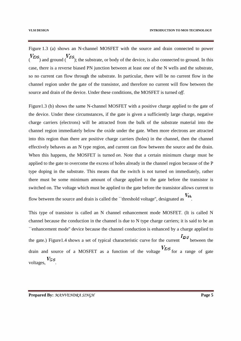
Figure 1.3 (a) shows an N-channel MOSFET with the source and drain connected to power
( ) and ground ( ); the substrate, or body of the device, is also connected to ground. In this
case, there is a reverse biased PN junction between at least one of the N wells and the substrate,
so no current can flow through the substrate. In particular, there will be no current flow in the
channel region under the gate of the transistor, and therefore no current will flow between the
source and drain of the device. Under these conditions, the MOSFET is turned off.
Figure1.3 (b) shows the same N-channel MOSFET with a positive charge applied to the gate of
the device. Under these circumstances, if the gate is given a sufficiently large charge, negative
charge carriers (electrons) will be attracted from the bulk of the substrate material into the
channel region immediately below the oxide under the gate. When more electrons are attracted
into this region than there are positive charge carriers (holes) in the channel, then the channel
effectively behaves as an N type region, and current can flow between the source and the drain.
When this happens, the MOSFET is turned on. Note that a certain minimum charge must be
applied to the gate to overcome the excess of holes already in the channel region because of the P
type doping in the substrate. This means that the switch is not turned on immediately, rather
there must be some minimum amount of charge applied to the gate before the transistor is
switched on. The voltage which must be applied to the gate before the transistor allows current to
flow between the source and drain is called the ``threshold voltage'', designated as .
This type of transistor is called an N channel enhancement mode MOSFET. (It is called N
channel because the conduction in the channel is due to N type charge carriers; it is said to be an
``enhancement mode'' device because the channel conduction is enhanced by a charge applied to
the gate.) Figure1.4 shows a set of typical characteristic curve for the current between the
drain and source of a MOSFET as a function of the voltage for a range of gate
voltages, .

VLSI DESIGN INTRODUCTION TO MOS TECHNOLOGY
Prepared By: MANVENDRA SINGH Page 6
Figure:1.4 characteristic curve enhancement mode
A second type of MOSFET can also be constructed; this type of device is commonly used in
purely NMOS designs, but is not used in CMOS designs. (Presently, we only have access to
CMOS processes.) This type of MOSFET, the ``depletion mode MOSFET'', acts as a ``normally
closed'' switch. Its behavior can qualitatively be explained with reference to Figure 1.5 which
shows an N channel depletion mode MOSFET.

VLSI DESIGN INTRODUCTION TO MOS TECHNOLOGY
Prepared By: MANVENDRA SINGH Page 7
Figure: 1.5 (a) N channel depletion mode MOSFET Figure: 1.5 (b) P channel depletion
mode MOSFET
In the depletion mode MOSFET, a thin layer of semiconductor material immediately beneath the
gate oxide is permanently doped with the same type material as the source and drain regions (but
different from the bulk of the substrate semiconductor material). This thin layer allows
conduction to occur in the channel region when no charge is applied to the gate. If a negative
charge is applied to the gate, then the negative charge carriers in the thin N-doped region
immediately beneath the gate oxide will be repelled from this region, leaving no free charge
carriers, and conduction will cease. In the depletion mode MOSFET, a charge (with the same
polarity as the drain dopant) applied to the gate turns the transistor off.
Depletion mode MOSFETs find their most common use not as switches but as resistors. As a
permanently ``on'' transistor, the device has a high resistance compared with the doped
semiconductor material itself, and the resistance is readily variable by modifying the size of the
transistor. (At fabrication time, the resistance can be modified by varying the number of ions
which are implanted in the gate region of the device). The commonly used circuit symbols for N-
and P- channel enhancement and depletion mode MOSFETs are shown in Figure 1.6. Figure 1.6
(a) shows the commonly used circuit symbols for P- and N- channel enhancement mode
MOSFETs; the corresponding circuit symbols for depletion mode devices are shown in Figure
1.6 (b).

VLSI DESIGN INTRODUCTION TO MOS TECHNOLOGY
Prepared By: MANVENDRA SINGH Page 8
Figure: 1.6 N- and P- channel enhancement and depletion mode MOSFETs
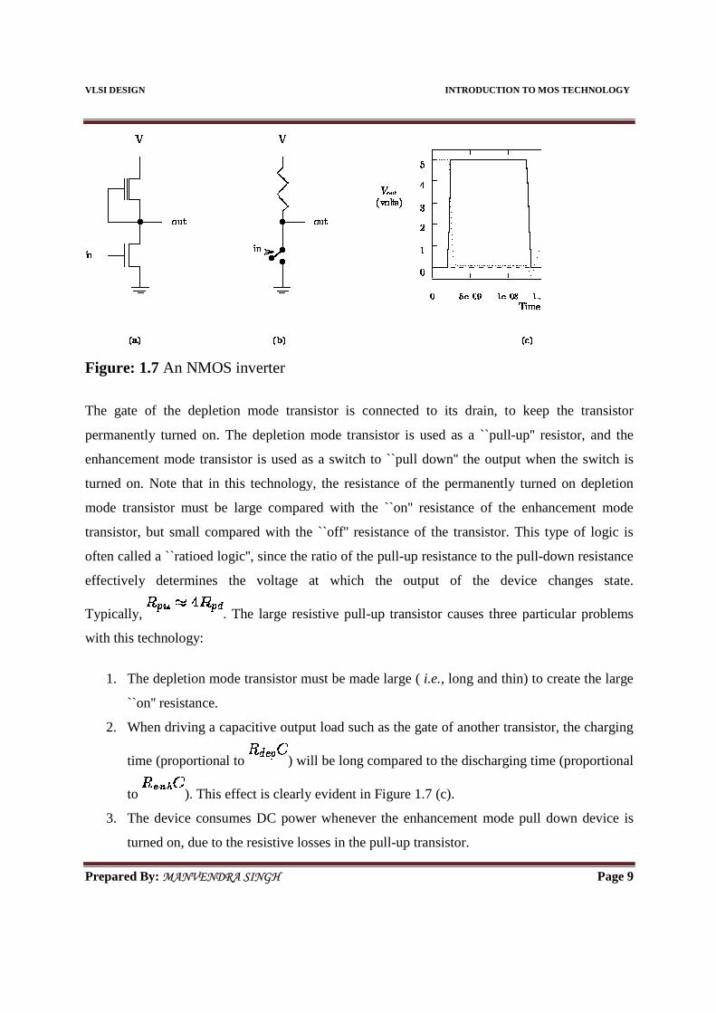
Both enhancement and depletion mode transistors are used in many of today's microelectronic
circuits. The most popular circuit technology using both enhancement and depletion mode
devices is the conventional NMOS technology. In this technology, depletion mode transistors are
mainly as resistors, and enhancement mode transistors are used as switches. Figure 1.7 shows a
typical inverter implemented in this technology, together with its switch equivalent. Also shown
is a plot of the output of a typical example of such an inverter for a given input pulse. (The input
pulse has a rise and fall time of 0.5 ns.)
VLSI DESIGN INTRODUCTION TO MOS TECHNOLOGY
Prepared By: MANVENDRA SINGH Page 9
Figure: 1.7 An NMOS inverter
The gate of the depletion mode transistor is connected to its drain, to keep the transistor
permanently turned on. The depletion mode transistor is used as a ``pull-up'' resistor, and the
enhancement mode transistor is used as a switch to ``pull down'' the output when the switch is
turned on. Note that in this technology, the resistance of the permanently turned on depletion
mode transistor must be large compared with the ``on'' resistance of the enhancement mode
transistor, but small compared with the ``off'' resistance of the transistor. This type of logic is
often called a ``ratioed logic'', since the ratio of the pull-up resistance to the pull-down resistance
effectively determines the voltage at which the output of the device changes state.
Typically, . The large resistive pull-up transistor causes three particular problems
with this technology:
1. The depletion mode transistor must be made large ( i.e., long and thin) to create the large
``on'' resistance.
2. When driving a capacitive output load such as the gate of another transistor, the charging
time (proportional to ) will be long compared to the discharging time (proportional
to ). This effect is clearly evident in Figure 1.7 (c).
3. The device consumes DC power whenever the enhancement mode pull down device is
turned on, due to the resistive losses in the pull-up transistor.

VLSI DESIGN INTRODUCTION TO MOS TECHNOLOGY
Prepared By: MANVENDRA SINGH Page 10
The third problem becomes more serious as feature sizes for transistors decrease, because the
number of such resistors per unit area increases, and the devices may not dissipate the heat as
well, resulting in device failure due to overheating.
1.Types of FETs
The family of FETs may be divided into :
(i) Junction FET
(ii) Depletion Mode MOSFET
(iii) Enhancement Mode MOSFET
(i) JFET Definition
•JFET is a unipolar-transistor, which acts as a voltage controlled current device and is a device
in which current at two electrodes is controlled by
the action of an electric field at a reversed biased p-n junction.
(ii) Enhancement Mode MOSFET
The Insulated Gate FET (IGFET).
The Metal Oxide Silicon FET (MOSFET) or Metal Oxide Silicon Transistor (M.O.S.T.) has an
even higher input resistance (typically 1011to 1015 ohms) than that of the JFET. In the MOSFET
device the gate is completely insulated from the rest of the transistor by a very thin layer of metal
VLSI DESIGN INTRODUCTION TO MOS TECHNOLOGY
Prepared By: MANVENDRA SINGH Page 11
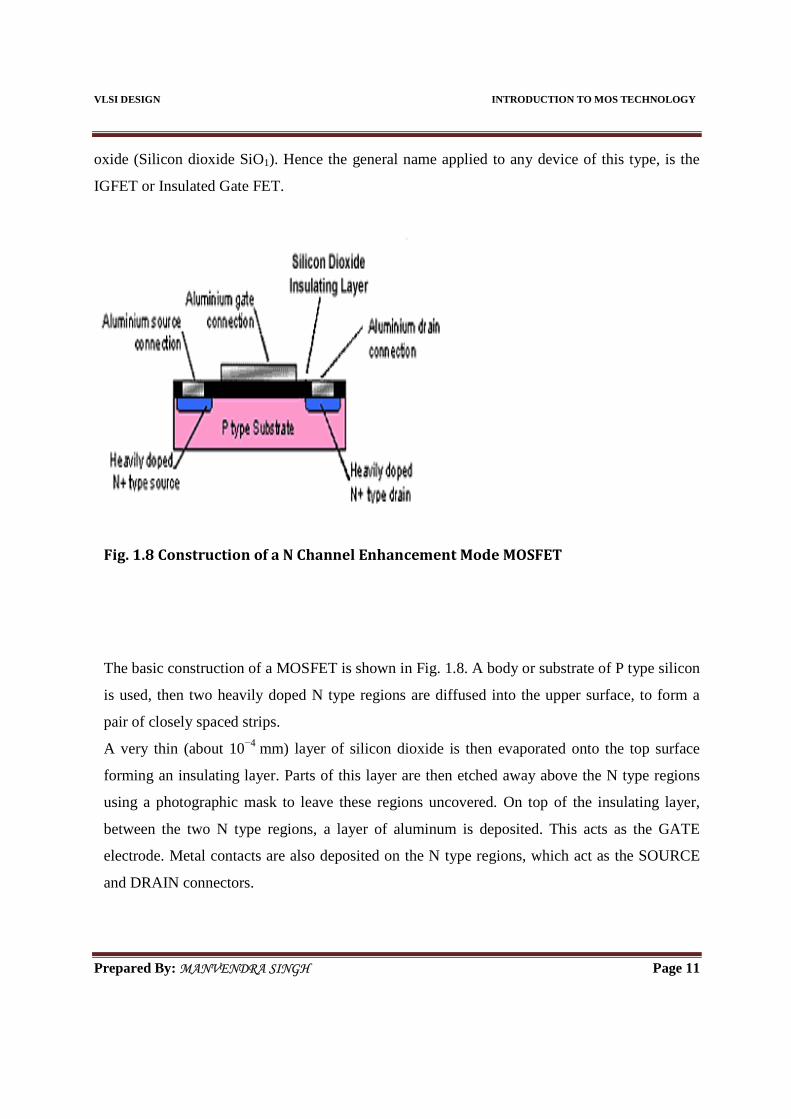
oxide (Silicon dioxide SiO1). Hence the general name applied to any device of this type, is the
IGFET or Insulated Gate FET.
Fig. 1.8 Construction of a N Channel Enhancement Mode MOSFET
The basic construction of a MOSFET is shown in Fig. 1.8. A body or substrate of P type silicon
is used, then two heavily doped N type regions are diffused into the upper surface, to form a
pair of closely spaced strips.
A very thin (about 10−4 mm) layer of silicon dioxide is then evaporated onto the top surface
forming an insulating layer. Parts of this layer are then etched away above the N type regions
using a photographic mask to leave these regions uncovered. On top of the insulating layer,
between the two N type regions, a layer of aluminum is deposited. This acts as the GATE
electrode. Metal contacts are also deposited on the N type regions, which act as the SOURCE
and DRAIN connectors.

VLSI DESIGN INTRODUCTION TO MOS TECHNOLOGY
Prepared By: MANVENDRA SINGH Page 12
Fig.1.9 Enhancement Mode Operation.
The gate has a voltage applied to it that makes it positive with respect to the source. This causes
holes in the P type layer close to the silicon dioxide layer beneath the gate to be repelled down
into the P type substrate, and at the same time this positive potential on the gate attracts free
electrons from the surrounding substrate material. These free electrons form a thin layer of
charge carriers beneath the gate electrode (they can't reach the gate because of the insulating
silicon dioxide layer) bridging the gap between the heavily doped source and drain areas. This

VLSI DESIGN INTRODUCTION TO MOS TECHNOLOGY
Prepared By: MANVENDRA SINGH Page 13
layer is sometimes called an "inversion layer" because applying the gate voltage has caused the
P type material immediately under the gate to firstly become "intrinsic" (with hardly any charge
carriers) and then an N type layer within the P type substrate.
Any further increase in the gate voltage attracts more charge carriers into the inversion layer, so
reducing its resistance, and increasing current flow between source and drain. Reducing the
gate source voltage reduces current flow. When the power is switched off, the area beneath the
gate reverts to P type once more.
As well as the type described above, devices having N type substrates and P type (inversion
layer) channels are also available. Operation is identical, but of course the polarity of the gate
voltage is reversed.
This method of operation is called "ENHANCEMENT MODE" as the application of gate
source voltage makes a conducting channel "grow", therefore it enhances the channel. Other
devices are available in which the application of a bias voltage reduces or "depletes" the
conducting channel.
Fig. 1.10 Circuit Symbols for Enhancement Mode MOSFETs (IGFETs)

VLSI DESIGN INTRODUCTION TO MOS TECHNOLOGY
Prepared By: MANVENDRA SINGH Page 14
(iii) Depletion Mode MOSFET
Fig: 1.11 Depletion Mode N Channel MOSFET
The depletion mode MOSFET shown as a N channel device (P channel is also available) in Fig
1.11 is more usually made as a discrete component, i.e. a single transistor rather than IC form.
In this device a thin layer of N type silicon is deposited just below the gate−insulating layer,
and forms a conducting channel between source and drain.
Therefore when the gate source voltage VGS is zero, current (in the form of free electrons) can
flow between source and drain. Note that the gate is totally insulated from the channel by the
layer of silicon dioxide. Now that a conducting channel is present the gate does not need to
cover the full width between source and drain. Because the gate is totally insulated from the
rest of the transistor this device, like other IGFETs, has a very high input resistance.

VLSI DESIGN INTRODUCTION TO MOS TECHNOLOGY
Prepared By: MANVENDRA SINGH Page 15
Fig. 1.11Operation of a Depletion Mode MOSFET
In the N channel device, shown in Fig. 1.11 the gate is made negative with respect to the
source, which has the effect of creating a depletion area, free from charge carriers, beneath the
gate. This restricts the depth of the conducting channel, so increasing channel resistance and
reducing current flow through the device.
Depletion mode MOSFETS are also available in which the gate extends the full width of the
channel (from source to drain). In this case it is also possible to operate the transistor in
enhancement mode. This is done by making the gate positive instead of negative. The positive
voltage on the gate attracts more free electrons into the conducing channel, while at the same
time repelling holes down into the P type substrate. The more positive the gate potential, the
deeper, and lower resistance is the channel. Increasing positive bias therefore increases current
flow. This useful depletion/enhancement version has the disadvantage that, as the gate area is
increased, the gate capacitance is also larger than true depletion types. This can present
difficulties at higher frequencies.

VLSI DESIGN INTRODUCTION TO MOS TECHNOLOGY
Prepared By: MANVENDRA SINGH Page 16
Fig. 1.13 Circuit Symbols for Depletion Mode MOSFETs (IGFETs)
Notice the solid bar between source and drain, indicating the presence of a conducting channel.
Note: Making the gate more negative reduces conduction between source & drain In N channel
devices, but increases conduction between source & drain In P channel devices.
· Applications of FETs
Although FETs have a lower gain than bipolar transistors, their very high input impedance
makes them suitable for applications where input signals may be severely reduced if applied to
a bipolar transistor base that needs base current to operate. The planar technology used to make
FETs is the same as that used to make integrated circuits, so most of the transistors found in
I / Cs are of this type. A useful feature of FETs is that they tend to produce less background
noise than Bipolar types and so are useful in the initial stages of systems such as amplifiers;
radios etc. where signal levels are very small and could be swamped by excessive background
noise.
3. THRESHOLD VOLTAGE
The threshold voltage of a MOSFET is usually defined as the gate voltage where an inversion
layer forms at the interface between the insulating layer (oxide) and the substrate (body) of
the transistor. The purpose of the inversion layer's forming is to allow the flow of electrons
through the gate-source junction. The creation of this layer is described next. In an n-MOSFET

VLSI DESIGN INTRODUCTION TO MOS TECHNOLOGY
Prepared By: MANVENDRA SINGH Page 17
the substrate of the transistor is composed of p-type silicon (see doping (semiconductor)), which
has positively charged mobile holes as carriers. When a positive voltage is applied on the gate,
an electric field causes the holes to be repelled from the interface, creating a depletion
region containing immobile negatively charged acceptor ions. A further increase in the gate
voltage eventually causes electrons to appear at the interface, in what is called an inversion layer,
or channel. Historically the gate voltage at which the electron density at the interface is the same
as the hole density in the neutral bulk material is called the threshold voltage. Practically
speaking the threshold voltage is the voltage at which there are sufficient electrons in the
inversion layer to make a low resistance conducting path between the MOSFET source and
drain.
In the figures, the source (left side) and drain (right side) are labeled n+ to indicate heavily
doped (blue) n-regions. The depletion layer dopant is labeled NA− to indicate that the ions in the
(pink) depletion layer are negatively charged and there are very few holes. In the (red) bulk the
number of holes p = NA making the bulk charge neutral.
If the gate voltage is below the threshold voltage (top figure), the transistor is turned off and
ideally there is no current from the drain to the source of the transistor. In fact, there is a current
even for gate biases below threshold (subthreshold leakage) current, although it is small and
varies exponentially with gate bias.
If the gate voltage is above the threshold voltage (lower figure), the transistor is turned on, due to
there being many electrons in the channel at the oxide-silicon interface, creating a low-resistance
channel where charge can flow from drain to source. For voltages significantly above threshold,
this situation is called strong inversion. The channel is tapered when VD > 0 because the voltage
drop due to the current in the resistive channel reduces the oxide field supporting the channel as
the drain is approached.
· In modern devices the threshold voltage is a much less clear-cut parameter subject to
variation with the biases applied to the device; see drain induced barrier lowering.

VLSI DESIGN INTRODUCTION TO MOS TECHNOLOGY
Prepared By: MANVENDRA SINGH Page 18
Fig. 1.14.MOSFET Scaling and Small Geometry Effects
To increase the number of devices per IC, the device dimensions had to be shrunk from one
generation to another (i.e. scaled down)
· In theory, there are two methods of scaling:
1. Full-Scaling (also called Constant-Field scaling): In this method the device dimensions (both
horizontal and vertical) are scaled down by 1/S, where S is the scaling factor. In order to
keep the electric field constant within the device, the voltages have to be scaled also by 1/S
such that the ratio between voltage and distance (which represents the electric field)
remain constant. The threshold voltage is also scaled down by the same factor as the
voltage to preserve the functionality of the circuits and the noise margins relative to one
another. As a result of this type of scaling the currents will be reduced and hence the total
power per transistor (P=IxV) will also be reduced, however the power density will remain
constant since the number of transistors per unit area will increase. This means that the
total chip power will remain constant if the chip size remains the same (this usually the
case).
Scaling
VLSI DESIGN INTRODUCTION TO MOS TECHNOLOGY
Prepared By: MANVENDRA SINGH Page 19
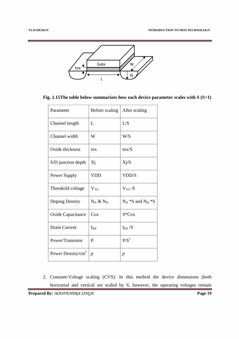
Fig. 1.15The table below summarizes how each device parameter scales with S (S>1)
Parameter Before scaling After scaling
Channel length L L/S
Channel width W W/S
Oxide thickness tox tox/S
S/D junction depth Xj Xj/S
Power Supply VDD VDD/S
Threshold voltage VTO VTO /S
Doping Density NA & ND NA *S and ND *S
Oxide Capacitance Cox S*Cox
Drain Current IDS IDS /S
Power/Transistor P P/S1
Power Density/cm1 p p
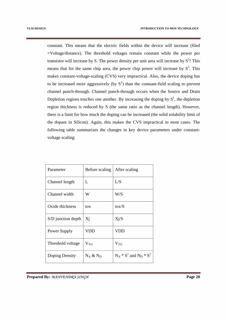
2. Constant-Voltage scaling (CVS): In this method the device dimensions (both
horizontal and vertical are scaled by S, however, the operating voltages remain
W Gate
L
tox
Xj
VLSI DESIGN INTRODUCTION TO MOS TECHNOLOGY
Prepared By: MANVENDRA SINGH Page 20
constant. This means that the electric fields within the device will increase (filed
=Voltage/distance). The threshold voltages remain constant while the power per
transistor will increase by S. The power density per unit area will increase by S3! This
means that for the same chip area, the power chip power will increase by S3. This
makes constant-voltage-scaling (CVS) very impractical. Also, the device doping has
to be increased more aggressively (by S1) than the constant-field scaling to prevent
channel punch-through. Channel punch-through occurs when the Source and Drain
Depletion regions touches one another. By increasing the doping by S1, the depletion
region thickness is reduced by S (the same ratio as the channel length). However,
there is a limit for how much the doping can be increased (the solid solubility limit of
the dopant in Silicon). Again, this makes the CVS impractical in most cases. The
following table summarizes the changes in key device parameters under constant-
voltage scaling:
Parameter Before scaling After scaling
Channel length L L/S
Channel width W W/S
Oxide thickness tox tox/S
S/D junction depth Xj Xj/S
Power Supply VDD VDD
Threshold voltage VTO VTO
Doping Density NA & ND NA * S1 and ND * S1

VLSI DESIGN INTRODUCTION TO MOS TECHNOLOGY
Prepared By: MANVENDRA SINGH Page 21
Oxide Capacitance Cox S*Cox
Drain Current IDS IDS * S
Power/Transistor P P*S
Power Desity/cm1 p p * S3
In almost all cases, the scaling is a combination of constant-field scaling and constant-voltage
scaling, such that the number of devices is increased and the total power/chip does not increase
much.
CMOS fabrication can be accomplished using either of the three technologies:
N-well/P-well technologies
Twin well technology
Silicon On Insulator (SOI)
Twin Well Technology
Using twin well technology, we can optimise NMOS and PMOS transistors separately. This
means that transistor parameters such as threshold voltage, body effect and the channel
transconductance of both types of transistors can be tuned independenly.
n+ or p+ substrate, with a lightly doped epitaxal layer on top, forms the starting material for this
technology. The n-well and p-well are formed on this epitaxial layer which forms the actual
substrate. The dopant concentrations can be carefully optimized to produce the desired device
characterisitcs because two independent doping steps are performed to create the well regions.

VLSI DESIGN INTRODUCTION TO MOS TECHNOLOGY
Prepared By: MANVENDRA SINGH Page 22
The conventional n-well CMOS process suffers from, among other effects, the problem of
unbalanced drain parasitics since the doping density of the well region typically being about one
order of magnitude higher than the substrate. This problem is absent in the twin-tub process.
Silicon on Insulator (SOI)
To improve process characteristics such as speed and latch-up susceptibility, technologists have
sought to use an insulating substrate instead of silicon as the substrate material.
Completely isolated NMOS and PMOS transistors can be created virtually side by side on an
insulating substrate (eg. sapphire) by using the SOI CMOS technology.
This technology offers advantages in the form of higher integration density (because of the
absence of well regions), complete avoidance of the latch-up problem, and lower parasitic
capacitances compared to the conventional n-well or twin-tub CMOS processes.
But this technology comes with the disadvantage of higher cost than the standard n-well CMOS
process. Yet the improvements of device performance and the absence of latch-up problems can
justify its use,especially in deep submicron devices.
N-well Technology
In this discussion we will concentrate on the well established n-well CMOS fabrication
technology, which requires that both n-channel and p-channel transistors be built on the same
chip substrate. To accomodate this, special regions are created with a semiconductor type
opposite to the substrate type. The regions thus formed are called wells or tubs. In an n-type
substrate, we can create a p-well or alternatively, an n-well is created in a p-type substrate. We
present here a simple n-well CMOS fabrication technology, in which the NMOS transistor is
created in the p-type substrate, and the PMOS in the n-well, which is built-in into the p-type
substrate.
Historically, fabrication started with p-well technology but now it has been completely shifted to
n-well technology. The main reason for this is that, "n-well sheet resistance can be made lower
than p-well sheet resistance" (electrons are more mobile than holes).

VLSI DESIGN INTRODUCTION TO MOS TECHNOLOGY
Prepared By: MANVENDRA SINGH Page 23
The simplified process sequence for the fabrication of CMOS integrated circuits on a p-type
silicon substrate is as follows:
· N-well regions are created for PMOS transistors, by impurity implantation into the
substrate
· This is followed by the growth of a thick oxide in the regions surround the NMOS and
PMOS active regions.
· The thin gate oxide is subsequently grown on the surface through thermal oxidation.
· After this n+ and p+ regions (source, drain and channel-stop implants) are created.
· The metallization step (creation of metal interconnects) forms the final step in this
process

VLSI DESIGN INTRODUCTION TO MOS TECHNOLOGY
Prepared By: MANVENDRA SINGH Page 24
Fig no
Fig. 1.16 Simplified Process Sequence For Fabrication Of CMOS ICs
The integrated circuit may be viewed as a set of patterned layers of doped silicon, polysilicon,
metal and insulating silicon dioxide, since each processing step requires that certain areas are
defined on chip by appropriate masks. A layer is patterned before the next layer of material is
applied on the chip. A process, called lithography, is used to transfer a pattern to a layer. This
must be repeated for every layer, using a different mask, since each layer has its own distinct
requirements.
VLSI DESIGN INTRODUCTION TO MOS TECHNOLOGY
Prepared By: MANVENDRA SINGH Page 25
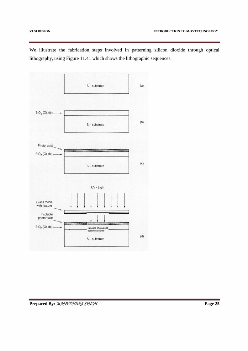
We illustrate the fabrication steps involved in patterning silicon dioxide through optical
lithography, using Figure 11.41 which shows the lithographic sequences.

VLSI DESIGN INTRODUCTION TO MOS TECHNOLOGY
Prepared By: MANVENDRA SINGH Page 26
Fig. 1.17 Process steps required for patterning of silicon dioxide

VLSI DESIGN INTRODUCTION TO MOS TECHNOLOGY
Prepared By: MANVENDRA SINGH Page 27
N-well Technology
First an oxide layer is created on the substrate with thermal oxidation of the silicon surface. This
oxide surface is then covered with a layer of photoresist. Photoresist is a light-sensitive, acid-
resistant organic polymer which is initially insoluble in the developing solution. On exposure to
ultraviolet (UV) light, the exposed areas become soluble which can be etched away by etching
solvents. Some areas on the surface are covered with a mask during exposure to selectively
expose the photoresist. On exposure to UV light, the masked areas are shielded whereas those
areas which are not shielded become soluble.
There are two types of photoresists, positive and negative photoresist. Positive photoresist is
initially insoluble, but becomes soluble after exposure to UV light, where as negative photoresist
is initially soluble but becomes insoluble (hardened) after exposure to UV light. The process
sequence described uses positive photoresist. Negative photoresists are more sensitive to light,
but their photolithographic resolution is not as high as that of the positive photoresists. Hence,
the use of negative photoresists is less common in manufacturing high-density integrated
circuits.
The unexposed portions of the photoresist can be removed by a solvent after the UV exposure
step. The silicon dioxide regions not covered by the hardened photoresist is etched away by
using a chemical solvent (HF acid) or dry etch (plasma etch) process. On completion of this step,
we are left with an oxide window which reaches down to the silicon surface. Another solvent is
used to strip away the remaining photoresist from the silicon dioxide surface.
VLSI DESIGN INTRODUCTION TO MOS TECHNOLOGY
Prepared By: MANVENDRA SINGH Page 28
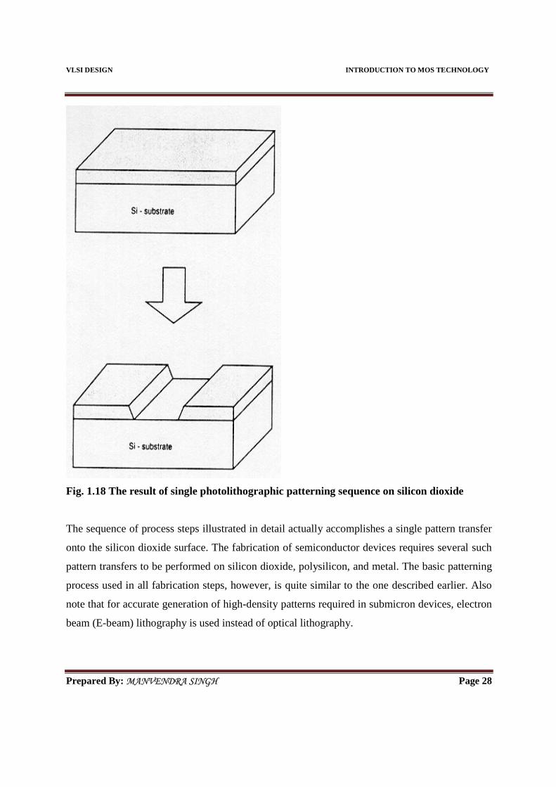
Fig. 1.18 The result of single photolithographic patterning sequence on silicon dioxide
The sequence of process steps illustrated in detail actually accomplishes a single pattern transfer
onto the silicon dioxide surface. The fabrication of semiconductor devices requires several such
pattern transfers to be performed on silicon dioxide, polysilicon, and metal. The basic patterning
process used in all fabrication steps, however, is quite similar to the one described earlier. Also
note that for accurate generation of high-density patterns required in submicron devices, electron
beam (E-beam) lithography is used instead of optical lithography.
VLSI DESIGN INTRODUCTION TO MOS TECHNOLOGY
Prepared By: MANVENDRA SINGH Page 29

VLSI DESIGN INTRODUCTION TO MOS TECHNOLOGY
Prepared By: MANVENDRA SINGH Page 30

VLSI DESIGN INTRODUCTION TO MOS TECHNOLOGY
Prepared By: MANVENDRA SINGH Page 31
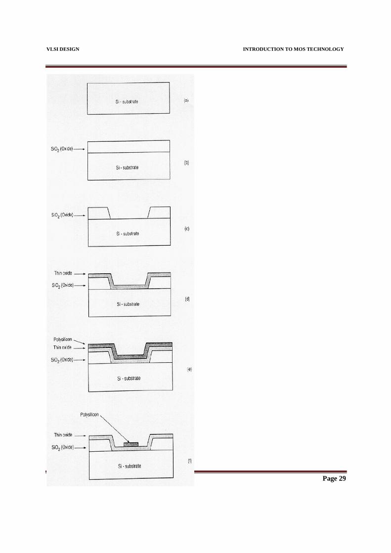
Fig. 1.19Process flow for the fabrication of an n-type MOSFET on p-type silicon
(Introduction of IC) Beyond the Syllabus
ICs were made possible by experimental discoveries showing that semiconductor devices could perform the functions of vacuum tubes and by mid-20th-century technology advancements in semiconductor device fabrication. The integration of large numbers of tiny transistors into a small chip was an enormous improvement over the manual assembly of circuits using discrete electronic components. The integrated circuit's mass production capability, reliability, and building-block approach to circuit design ensured the rapid adoption of standardized Integrated Circuits in place of designs using discrete transistors.
There are two main advantages of ICs over discrete circuits: cost and performance. Cost is low because the chips, with all their components, are printed as a unit by photolithography rather than being constructed one transistor at a time. Furthermore, much less material is used to construct a packaged IC die than to construct a discrete circuit. Performance is high because the components switch quickly and consume little power (compared to their discrete counterparts) as a result of the small size and close proximity of the components. As of 2012, typical chip areas range from a few square millimeters to around 450 mm2, with up to 9 million transistors per mm2.