subject: semiconductor and digital devices lab · pdf file · 2017-02-27subject:...
TRANSCRIPT

Department of Electrical & Electronics Engineering
LAB MANUAL
SUBJECT: Semiconductor and Digital Devices Lab
B.E/B.E MBA Second Year – III Semester (Branch: EEE)
University Institute of Engineering and Technology, Panjab University, Chandigarh

TABLE OF CONTENTS
S No.
Topic Page No.
1. Study of P-N Junction Diode Characteristics.
2. To Study the characteristics of transistor in Common Base configuration
3. To plot and study the input and output characteristics of BJT in common-emitter configuration
4. To study the drain characteristics of FET
5. To measure the voltage gain of a CE amplifier and plot the frequency response curve of the CE amplifier.
6. Study and Verification of Logic Gates
7. Study of various truth table of flip flops and conversion of one flip flop to another
8. Study of ADC and DAC using ADC0809
SCD LAB 1. P-N JUNCTION DIODE CHARACTERISTICS
AIM:-To observe and draw the Forward and Reverse bias V-I Characteristics of a P-N Junction diode. APPARATUS:-
P-N Diode IN4007. Regulated Power supply (0-30v) Resistor 1KΏ Ammeters (0-200 mA, 0-500mA) Voltmeter (0-20 V) Bread board Connecting wires
THEORY:-
A p-n junction diode conducts only in one direction. The V-I characteristics of the diode are curve between voltage across the diode and current through the diode. When external voltage is zero, circuit is open and the potential barrier does not allow the current to flow. Therefore, the circuit current is zero. When P-type (Anode is connected to +ve terminal and n- type (cathode) is Connected to –ve terminal of the supply voltage is known as forward bias. The potential barrier is reduced when diode is in the forward biased condition. At some forward voltage, the potential barrier altogether eliminated and current starts flowing through the diode and also in the circuit. The diode is said to be in ON state. The current increases with increasing forward voltage. When N-type (cathode) is connected to +ve terminal and P-type (Anode) is connected –ve terminal of the supply voltage is known as reverse bias and the potential barrier across the junction increases. Therefore, the junction resistance becomes very high and a very small current (reverse saturation current) flows in the circuit. The diode is said to be in OFF state. The reverse bias current due to minority charge carriers.
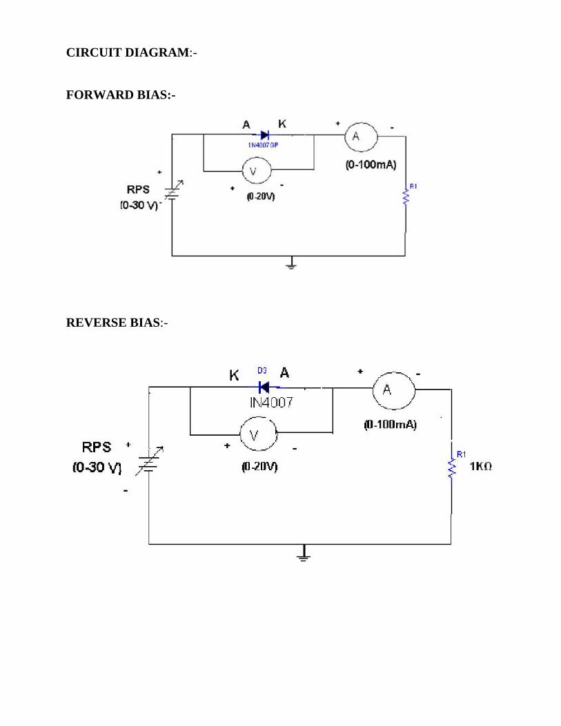
CIRCUIT DIAGRAM:- FORWARD BIAS:- REVERSE BIAS:-

MODEL WAVEFORM:- PROCEDURE:- FORWARD BIAS:- 1. Connections are made as per the circuit diagram. 2. for forward bias, the RPS +ve is connected to the anode of the diode and RPS –ve is connected to the cathode of the diode, 3. Switch on the power supply and increases the input voltage (supply voltage) in Steps. 4. Note down the corresponding current flowing through the diode and voltage across the diode for each and every step of the input voltage. 5. The reading of voltage and current are tabulated. 6. Graph is plotted between voltage and current.

OBSERVATION:- PROCEDURE:- REVERSE BIAS:- 1. Connections are made as per the circuit diagram 2 . For reverse bias, the RPS +ve is connected to the cathode of the diode and RPS –ve is connected to the anode of the diode. 3. Switch on the power supply and increase the input voltage (supply voltage) in Steps 4. Note down the corresponding current flowing through the diode voltage across the diode for each and every step of the input voltage. 5. The readings of voltage and current are tabulated 6. Graph is plotted between voltage and current. OBSEVATION:- RESULT: - Forward and Reverse Bias characteristics for a p-n diode is observed.

2. TRANSISTOR COMMON -BASE CONFIGURATION AIM: 1.To observe and draw the input and output characteristics of a
transistor connected in common base configuration. 2. To find ά of the given transistor.
APPARATUS:
Transistor, BC 107 Regulated power supply (0-30V, 1A) Voltmeter (0-20V) Ammeters (0-100mA) Resistor, 1000 _. Bread board Connecting wires
THEORY:
A transistor is a three terminal active device. T he terminals are emitter, base, collector. In CB configuration, the base is common to both input (emitter) and output (collector). For normal operation, the E-B junction is forward biased and C-B junction is reverse biased.
In CB configuration, IE is +ve, IC is –ve and IB is –ve. So,
VEB=f1 (VCB,IE) and IC=f2 (VCB,IB)
With an increasing the reverse collector voltage, the space-charge width
at the output junction increases and the effective base width ‘W’ decreases. This phenomenon is known as “Early effect”. Then, there will be less chance for recombination within the base region. With increase of charge gradient with in the base region, the current of minority carriers injected across the emitter junction increases.The current amplification factor of CB configuration is given by,
ά= _IC/ _IE

CIRCUIT DIAGRAM PROCEDURE: INPUT CHARACTERISTICS: 1. Connections are made as per the circuit diagram. 2. For plotting the input characteristics, the output voltage VCE is kept constant at 0V and for different values of VEB note down the values of IE. 3. Repeat the above step keeping VCB at 2V, 4V, and 6V.All the readings are tabulated. 4. A graph is drawn between VEB and IE for constant VCB. OUTPUT CHARACTERISTICS: 1. Connections are made as per the circuit diagram. 2. For plotting the output characteristics, the input IE iskept constant at 10m A and for different values of VCB, note down the values of IC. 3. Repeat the above step for the values of IE at 20 mA, 40 mA, and 60 mA, all the readings are tabulated. 4. A graph is drawn between VCB and Ic for constant IE
OBSERVATIONS: INPUT CHARACTERISTICS:
Sr VCB = 0V VCB = 1V VCB = 2V No.
VEB(V) IE(mA) VEB(V) IE(mA) VEB(V) IE(mA)
OUTPUT CHARACTERISTICS:
Sr IE=10mA IE=20mA IE=30mA No.
VCB(V) IC(mA) VCB(V) IC(mA) VCB(V) IC(mA)
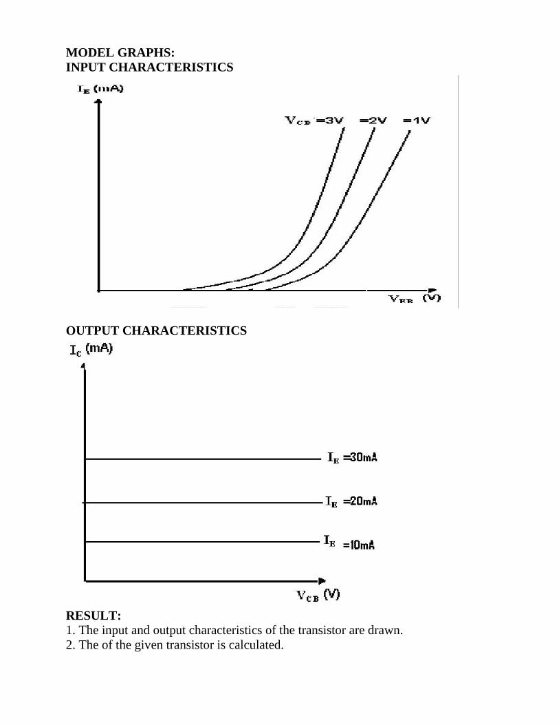
MODEL GRAPHS: INPUT CHARACTERISTICS OUTPUT CHARACTERISTICS RESULT: 1. The input and output characteristics of the transistor are drawn. 2. The of the given transistor is calculated.

3. TRANSISTOR CE CHARACTERSTICS AIM: 1. To draw the input and output characteristics of transistor connected in CE configuration
2. To find of the given transistor. APPARATUS:
Transistor (BC 107) R.P.S (O-30V) 2Nos Voltmeters (0-20V) 2Nos Ammeters (0-200µA) (0-500mA) Resistors 1Kohm Bread board
THEORY:
A transistor is a three terminal device. The terminals are emitter, base, collector. In common emitter configuration, input voltage is applied between base and emitter terminals and output is taken across the collector and emitter terminals. Therefore the emitter terminal is common to both input and output. The input characteristics resemble that of a forward biased diode curve. This is expected since the Base-Emitter junction of the transistor is forward biased. As compared to CB arrangement IB increases less rapidly with VBE . Therefore input resistance of CE circuit is higher than that of CB circuit. The output characteristics are drawn between Ic and VCE at constant IB. the collector current varies with VCE unto few volts only. After this the collector current becomes almost constant, and independent of VCE. The value of VCE up to which the collector current changes with V CE is known as Knee voltage. The transistor always operated in the region above Knee voltage, IC is always constant and is approximately equal to IB. The current amplification factor of CE configuration is given by
= _IC/_IB

CIRCUIT DIAGRAM: PROCEDURE: INPUT CHARECTERSTICS: 1. Connect the circuit as per the circuit diagram. 2. For plotting the input characteristics the output voltage VCE is kept Constant at 1V and for different values of VBE. Note down the values of IC 3. Repeat the above step by keeping VCE at 2V and 4V. 4. Tabulate all the readings. 5. Plot the graph between VBE and IB for constant VCE OUTPUT CHARACTERSTICS: 1. Connect the circuit as per the circuit diagram 2. For plotting the output characteristics the input current IB is kept constant At 10µA and for different values of VCE note down the values of IC 3. Repeat the above step by keeping IB at 75 µA 100 µA 4. Tabulate the all the readings 5. Plot the graph between VCE and IC for constant IB

OBSERVATIONS: INPUT CHARACTERISTICS: Sr VCE = 1V VCE = 2V VCE = 4V
No.
VBE(V) IB(uA) VBE(V) IB(uA) VBE(V) IB(uA)
OUT PUT CHAREACTARISTICS:
Sr IB = 50uA IB = 75uA IB = 100uA
No.
VCE(V) IC(mA) VCE(V) IC(mA) VCE(V) IC(mA)

MODEL GRAPHS: INPUT CHARACTERSTICS:

OUTPUT CHARECTERSTICS: RESULT: 1. The input and output characteristics of a transistor in CE configuration are drawn 2. The of a given transistor is calculated.
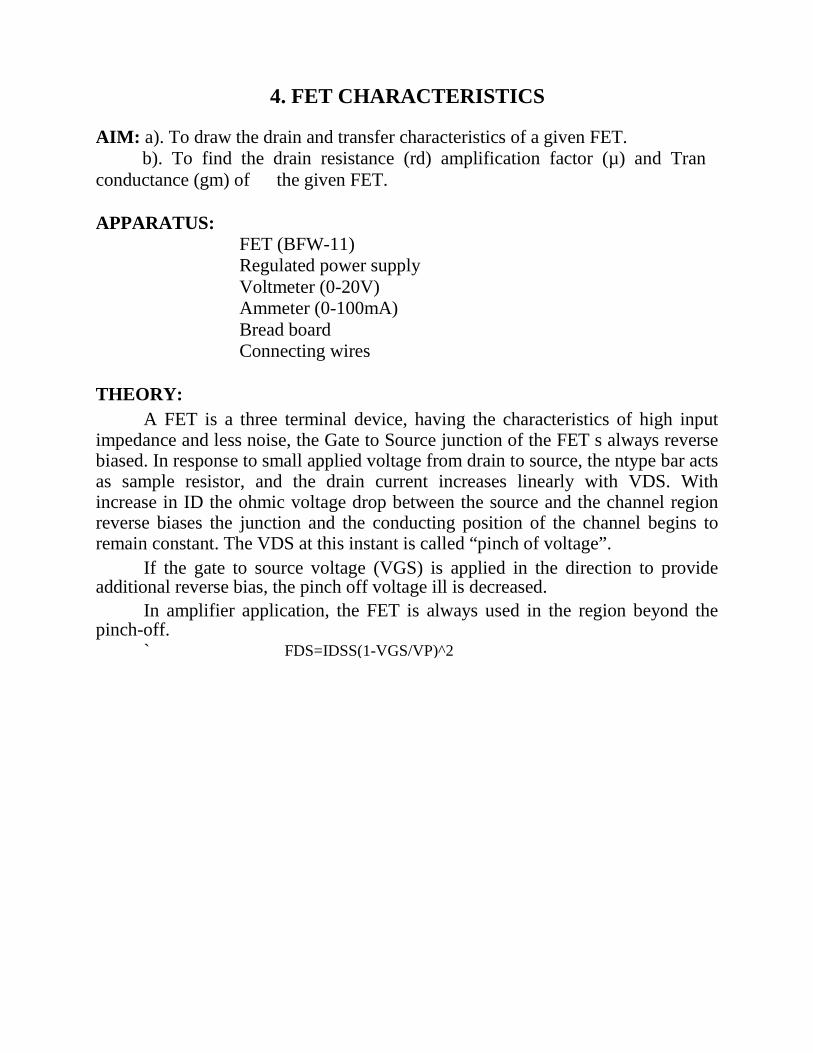
4. FET CHARACTERISTICS AIM: a). To draw the drain and transfer characteristics of a given FET.
b). To find the drain resistance (rd) amplification factor (µ) and Tran conductance (gm) of the given FET. APPARATUS:
FET (BFW-11) Regulated power supply Voltmeter (0-20V) Ammeter (0-100mA) Bread board Connecting wires
THEORY:
A FET is a three terminal device, having the characteristics of high input impedance and less noise, the Gate to Source junction of the FET s always reverse biased. In response to small applied voltage from drain to source, the ntype bar acts as sample resistor, and the drain current increases linearly with VDS. With increase in ID the ohmic voltage drop between the source and the channel region reverse biases the junction and the conducting position of the channel begins to remain constant. The VDS at this instant is called “pinch of voltage”.
If the gate to source voltage (VGS) is applied in the direction to provide additional reverse bias, the pinch off voltage ill is decreased.
In amplifier application, the FET is always used in the region beyond the pinch-off.
` FDS=IDSS(1-VGS/VP)^2

CIRCUIT DIAGRAM PROCEDURE: 1. All the connections are made as per the circuit diagram. 2. To plot the drain characteristics, keep VGS constant at 0V. 3. Vary the VDD and observe the values of VDS and ID. 4. Repeat the above steps 2, 3 for different values of VGS at 0.1V and 0.2V. 5. All the readings are tabulated. 6. To plot the transfer characteristics, keep VDS constant at 1V. 7. Vary VGG and observe the values of VGS and ID. 8. Repeat steps 6 and 7 for different values of VDS at 1.5 V and 2V. 9. The readings are tabulated. 10. From drain characteristics, calculate the values of dynamic resistance (rd) by using the formula
rd = _VDS/_ID 11. From transfer characteristics, calculate the value of transconductace (gm) By using the formula
Gm=_ID/_VDS 12. Amplification factor (µ) = dynamic resistance. Tran conductance
µ = _VDS/_VGS

OBSERVATIONS: DRAIN CHARACTERISTICS:
Sr VGS = 0V VGS = 0.1V VGS = 0.2V No.
VDS(V) ID(mA) VDS(V) ID(mA) VDS(V) ID(mA)
TRANSFER CHARACTERISTICS:
Sr VDS = 0.5V VDS = 1V VDS = 1.5V No.
VGS(V) ID(mA) VGS(V) ID(mA) VGS(V) ID(mA)

MODEL GRAPH: TRANSFER CHARACTERISTICS

DRAIN CHARACTERISTICS RESULT: 1. The drain and transfer characteristics of a given FET are drawn. 2. The dynamic resistance (rd), amplification factor (µ) and Tran conductance (gm) of the given FET are calculated.

5. TRANSISTOR CE AMPLIFIER
AIM: 1. To Measure the voltage gain of a CE amplifier
2. To draw the frequency response curve of the CE amplifier. APPARATUS:
Transistor BC-107 Regulated power Supply (0-30V, 1A) Function Generator CRO Resistors [33K., 3.3K., 330., 1.5K. 1K., 2.2K., 4.7K.] Capacitors- 10µF -2No 100µF Bread Board Connecting Wires.
THEORY:
The CE amplifier provides high gain &wide frequency response. The emitter lead is common to both input & output circuits and is grounded. The emitter-base circuit is forward biased. The collector current is controlled by the base current rather than emitter current. The input signal is applied to base terminal of the transistor and amplifier output is taken across collector terminal. A very small change in base current produces a much larger change in collector current. When +VE half-cycle is fed to the input circuit, it opposes the forward bias of the circuit which causes the collector current to decrease, it decreases the voltage more –VE. Thus when input cycle varies through a -VE half-cycle, increases the forward bias of the circuit, which causes the collector current to increases thus the output signal is common emitter amplifier is in out of phase with the input signal.

CIRCUIT DIAGRAM: PROCEDURE: 1. Connect the circuit as shown in circuit diagram 2. Apply the input of 20mV peak-to-peak and 1 KHz frequency using Function Generator 3. Measure the Output Voltage Vo (p-p) for various load resistors 4. Tabulate the readings in the tabular form. 5. The voltage gain can be calculated by using the expression Av= (V0/Vi) 6. For plotting the frequency response the input voltage is kept Constant at 20mV peak-to-peak and the frequency is varied from 100Hz to 1MHz Using function generator 7. Note down the value of output voltage for each frequency. 8. All the readings are tabulated and voltage gain in dB is calculated by Using the expression
Av=20 log10 (V0/Vi) 9. A graph is drawn by taking frequency on x-axis and gain in dB on y-axis on Semi-log graph.
The band width of the amplifier is calculated from the graph using the expression,

Bandwidth, BW=f2-f1 Where f1 lower cut-off frequency of CE amplifier, and Where f2 upper cut-off frequency of CE amplifier
The bandwidth product of the amplifier is calculated using the expression
Gain Bandwidth product=3-dBmidband gain X Bandwidth OBSERVATIONS:
Input voltage Vi=20mV
Load resistance Output Gain Gain in dB (KΏ) Voltage(Vo) Av= (Vo/Vi) Av =
20log10(Vo/Vi)
FREQUENCY RESPONSE: Vi=20mv
FREQUENCY(Hz) OUTPUT GAIN IN dB
VOLTAGE (V0) Av=20 log10 (V0/Vi)

MODELWAVE FORMS: INPUT WAVE FORM: OUTPUT WAVE FORM FREQUENCY RESPONSE RESULT: The voltage gain and frequency response of the CE amplifier are obtained. Also gain bandwidth product of the amplifier is calculated.

6. LOGIC GATES AIM: To study and verify the truth table of logic gates LEARNING OBJECTIVE:
• Identify various ICs and their specification. COMPONENTS REQUIRED:
o Logic gates (IC) trainer kit. o Connecting patch chords. o IC 7400, IC 7408, IC 7432, IC 7406, IC 7402, IC 7404, IC 7486
THEORY: The basic logic gates are the building blocks of more complex logic circuits. These logic gates perform the basic Boolean functions, such as AND, OR, NAND, NOR, Inversion, Exclusive-OR, Exclusive-NOR. Fig. below shows the circuit symbol, Boolean function, and truth. It is seen from the Fig that each gate has one or two binary inputs, A and B, and one binary output, C. The small circle on the output of the circuit symbols designates the logic complement. The AND, OR, NAND, and NOR gates can be extended to have more than two inputs. A gate can be extended to have multiple inputs if the binary operation it represents is commutative and associative. These basic logic gates are implemented as small-scale integrated circuits (SSICs) or as part of more complex medium scale (MSI) or very large-scale (VLSI) integrated circuits. Digital IC gates are classified not only by their logic operation, but also the specific logic-circuit family to which they belong. Each logic family has its own basic electronic circuit upon which more complex digital circuits and functions are developed. The following logic families are the most frequently used. TTL Transistor-transistor logic ECL Emitter-coupled logic MOS Metal-oxide semiconductor CMOS Complementary metal-oxide semiconductor TTL and ECL are based upon bipolar transistors. TTL has a well established popularity among logic families. ECL is used only in systems requiring high-speed operation. MOS and CMOS, are based on field effect transistors. They are widely used in large scale integrated circuits because of their high component density and relatively low power consumption. CMOS logic consumes far less power than MOS logic. There are various commercial integrated circuit chips available. TTL ICs are usually distinguished by numerical designation as the 5400 and 7400 series. PROCEDURE: 1. Check the components for their working. 2. Insert the appropriate IC into the IC base. 3. Make connections as shown in the circuit diagram. 4. Provide the input data via the input switches and observe the output on output LEDs


7. FLIP FLOPS AIM: Truth Table verification of
1) RS Flip Flop 2) T type Flip Flop. 3) D type Flip Flop. 4) JK Flip Flop. 5) JK Master Slave Flip Flop.
LEARNING OBJECTIVE:
To learn about various Flip-Flops To learn and understand the working of Master slave FF To learn about applications of FFs
Conversion of one type of Flip flop to another COMPONENTS REQUIRED: IC 7408, IC 7404, IC 7402, IC 7400, Patch Cords & IC Trainer Kit. THEORY: Logic circuits that incorporate memory cells are called sequential logic circuits; their output depends not only upon the present value of the input but also upon the previous values. Sequential logic circuits often require a timing generator (a clock) for their operation. The latch (flip-flop) is a basic bi-stable memory element widely used in sequential logic circuits. Usually there are two outputs, Q and its complementary value. Some of the most widely used latches are listed below. SR LATCH: An S-R latch consists of two cross-coupled NOR gates. An S-R flip-flop can also be design using cross-coupled NAND gates as shown. The truth tables of the circuits are shown below.
A clocked S-R flip-flop has an additional clock input so that the S and R inputs are active only when the clock is high. When the clock goes low, the state of flip-flop is latched and cannot change until the clock goes high again. Therefore, the clocked S-R flip-flop is also called “enabled” S-R flip-flop.
A D latch combines the S and R inputs of an S-R latch into one input by adding an inverter. When the clock is high, the output follows the D input, and when the clock goes low, the state is latched.
A S-R flip-flop can be converted to T-flip flop by connecting S input to Qb and R to Q.

1) S-R LATCH:
(A) LOGIC DIAGRAM (B) SYMBOL TRUTH TABLE
S R Q+
Q b+
0 0 Q
Q b
0 1 0 1
1 0 1 0
1 1 0* 0*
S R LATCH: TRUTH TABLE
S R Q+ Q b+
0 0 1* 1*
0 1 1 0
1 0 0 1
1 1 Q
Q b

2) SR FLIP FLOP:
CIRCUIT DIAGRAM:
(A) LOGIC DIAGRAM (B) SYMBOL
TRUTH TABLE
S R Q+ Q b+
0 0 Q
Q b
0 1 0 1
1 0 1 0
1 1 0* 0*

3) CONVERSION OF SR-FLIP FLOP TO T-FLIP FLOP (Toggle)
LOGIC DIAGRAM SYMBOL T FLIP FLOP USING IC 7476 TRUTH TABLE
T Qn + 1
0 Qn
1 Qn

4) CONVERSION OF SR-FLIP FLOP TO D-FLIP FLOP :
LOGIC DIAGRAM SYMBOL
D FLIP FLOP USING IC 7476 TRUTH TABLE CLOCK D Q+ Q+
0 X Q Q
1 0 0 1
1 1 1 0

5. CONVERSION OF SR-FLIP FLOP TO JK-FLIP FLOP
LOGIC DIAGRAM TRUTH TABLE
Clock J K Q+ Q’+ Comment
1 0 0 Q Q’ No
Change
1 0 1 0 1 Reset
1 1 0 1 0 Set
1 1 1 Q’ Q Toggle
LOGIC DIAGRAM TRUTH TABLE SD RD Clock J K Q Q’ Comment
0 0 Not Allowed
0 1 X X X 1 0 Set
1 0 X X X 0 1 Reset
1 1 1 0 0 NC NC Memory
1 1 1 0 1 0 1 Reset
1 1 1 1 0 1 0 Set
1 1 1 1 1 Q’ Q Toggle

6. JK MASTER SLAVE FLIP FLOP
LOGIC DIAGRAM
TRUTH TABLE
PRE = CLR = 1
Clock J K Q+ Q’+ Comment
1 0 0 Q Q’ No
Change
1 0 1 0 1 Reset
1 1 0 1 0 Set
1 1 1 Race Around
PROCEDURE: • Check all the components for their working. • Insert the appropriate IC into the IC base. • Make connections as shown in the circuit diagram.
Verify the Truth Table and observe the outputs.
33