sublvds to mipi csi-2 image sensor interface bridge soft ip user
TRANSCRIPT

SubLVDS to MIPI CSI-2 Image Sensor Interface Bridge Soft IP
User Guide
FPGA-IPUG-02006 Version 1.3
February 2017

SubLVDS to MIPI CSI-2 Image Sensor Interface Bridge Soft IP User Guide
© 2016-2017 Lattice Semiconductor Corp. All Lattice trademarks, registered trademarks, patents, and disclaimers are as listed at www.latticesemi.com/legal. All other brand or product names are trademarks or registered trademarks of their respective holders. The specifications and information herein are subject to change without notice.
2 FPGA-IPUG-02006-1.3
Contents 1. Introduction ................................................................................................................................................................... 4
1.1. Quick Facts .......................................................................................................................................................... 4 1.2. Features ............................................................................................................................................................... 4 1.3. Conventions......................................................................................................................................................... 4
1.3.1. Nomenclature ................................................................................................................................................. 4 1.3.2. Signal Names .................................................................................................................................................. 4
2. Functional Description .................................................................................................................................................. 5 2.1. Interface and Timing Diagram ............................................................................................................................. 6
2.1.1. SubLVDS Interface .......................................................................................................................................... 6 2.1.2. MIPI D-PHY Interface ...................................................................................................................................... 7
2.2. Clocking and Reset .............................................................................................................................................. 8 2.3. Module Descriptions ........................................................................................................................................... 9
2.3.1. SubLVDS Rx Wrapper .................................................................................................................................... 11 2.3.2. CMOS2DPHY ................................................................................................................................................. 11 2.3.3. IMX Framer ................................................................................................................................................... 11
3. Parameter Settings ..................................................................................................................................................... 12 4. IP Generation and Evaluation ..................................................................................................................................... 13
4.1. Licensing the IP .................................................................................................................................................. 13 4.2. Getting Started .................................................................................................................................................. 13 4.3. Creating IP in Clarity Designer ........................................................................................................................... 14 4.4. Generated IP Directory Structure and Files ....................................................................................................... 19 4.5. Running Functional Simulation ......................................................................................................................... 20 4.6. Simulation Strategies ........................................................................................................................................ 21 4.7. Simulation Environment .................................................................................................................................... 22 4.8. Instantiating the IP ............................................................................................................................................ 23 4.9. Synthesizing and Implementing the IP in a Top-Level Design ........................................................................... 23 4.10. Hardware Evaluation ......................................................................................................................................... 23
4.10.1. Enabling Hardware Evaluation in Diamond .................................................................................................. 23 4.11. Updating/Regenerating the IP........................................................................................................................... 24
4.11.1. Regenerating an IP in Clarity Designer ......................................................................................................... 24 References .......................................................................................................................................................................... 25 Technical Support Assistance ............................................................................................................................................. 25 Appendix A. Resource Utilization ....................................................................................................................................... 26 Appendix B. What is Not Supported ................................................................................................................................... 27 Revision History .................................................................................................................................................................. 28
SubLVDS to MIPI CSI-2 Image Sensor Interface Bridge Soft IP User Guide
© 2016-2017 Lattice Semiconductor Corp. All Lattice trademarks, registered trademarks, patents, and disclaimers are as listed at www.latticesemi.com/legal. All other brand or product names are trademarks or registered trademarks of their respective holders. The specifications and information herein are subject to change without notice.
FPGA-IPUG-02006-1.3 3
Figures Figure 2.1. SubLVDS Input Data, Clock and Sync Signal Timing (4k2k, 10-bit Data, 10-Lanes) ............................................. 6 Figure 2.2. High-Speed Data Transmission ........................................................................................................................... 8 Figure 2.3. SubLVDS to CSI-2 Clock Domains ........................................................................................................................ 8 Figure 2.4. Top Level Block Diagram ..................................................................................................................................... 9 Figure 4.1. Clarity Designer Window .................................................................................................................................. 13 Figure 4.2. Starting Clarity Designer from Diamond Design Environment ......................................................................... 14 Figure 4.3. Configuring SubLVDS to MIPI CSI-2 IP in Clarity Designer ................................................................................ 15 Figure 4.4. Configuration Tab in IP GUI .............................................................................................................................. 16 Figure 4.5. Video Tab in IP GUI ........................................................................................................................................... 17 Figure 4.6. Protocol Timing Parameters Tab in IP GUI........................................................................................................ 18 Figure 4.7. SubLVDS to MIPI CSI-2 IP Directory Structure .................................................................................................. 19 Figure 4.8. Simulation Environment Block Diagram ........................................................................................................... 21 Figure 4.9. Configuration with MISC_ON Disabled ............................................................................................................. 22 Figure 4.10. Configuration with MISC_ON Enabled ............................................................................................................ 22 Figure 4.11. IP Regeneration in Clarity Designer ................................................................................................................ 24
Tables Table 1.1. SubLVDS to MIPI CSI-2 IP Quick Facts .................................................................................................................. 4 Table 2.1. Sync Code Details ................................................................................................................................................. 7 Table 2.2. Top Level Port Description ................................................................................................................................. 10 Table 2.3. Indicator States .................................................................................................................................................. 11 Table 3.1. SubLVDS to CSI-2 IP Parameters ........................................................................................................................ 12 Table 4.1. Files Generated in Clarity Designer .................................................................................................................... 19 Table 4.2. Testbench Directives .......................................................................................................................................... 21 Table A.1. Resource Utilization* ......................................................................................................................................... 26

SubLVDS to MIPI CSI-2 Image Sensor Interface Bridge Soft IP User Guide
© 2016-2017 Lattice Semiconductor Corp. All Lattice trademarks, registered trademarks, patents, and disclaimers are as listed at www.latticesemi.com/legal. All other brand or product names are trademarks or registered trademarks of their respective holders. The specifications and information herein are subject to change without notice.
4 FPGA-IPUG-02006-1.3
1. Introduction Many Image Signal Processors (ISP) or Application Processors (AP) use the Mobile Industry Processor Interface (MIPI®)
Camera Serial Interface 2 (CSI-2) standard for image sensor inputs. However, some high resolution CMOS image sensors use a proprietary SubLVDS output format. The Lattice Semiconductor SubLVDS to MIPI CSI-2 Image Sensor Interface Bridge IP for Lattice Semiconductor CrossLink™ solves the interface mismatch between subLVDS output image sensor and an ISP/AP using MIPI CSI-2 interface.
This user guide is for SubLVDS to MIPI CSI-2 Image Sensor Interface Bridge Soft IP design version 1.2.
1.1. Quick Facts Table 1.1 provides quick facts about the SubLVDS to MIPI CSI-2 Image Sensor Interface Bridge IP for CrossLink devices.
Table 1.1. SubLVDS to MIPI CSI-2 IP Quick Facts
SubLVDS to MIPI CSI-2 IP Configuration
10-Lane Configuration
Core Requirements FPGA Families Supported CrossLink
Resource Utilization
Target Device LIF-MD6000-6MG81I
Data Path Width 10-bit (RAW10) or 12-bit (RAW12) input data to D-PHY serial data
LUTs 3711
sysMEM™ EBRs 12
Registers 2388
Design Tool Support
Lattice Implementation Lattice Diamond® 3.8
Synthesis Lattice Synthesis Engine (LSE)
Synopsys® Synplify Pro® L-2016.03L or later
Simulation Aldec® Active HDL™ 10.3 Lattice Edition
1.2. Features The key features of the SubLVDS to MIPI CSI-2 Image Sensor Interface Bridge IP are:
Supports four, six, eight or ten data lanes from an image sensor in 10-bit (RAW10) or 12-bit (RAW12) pixel widths
Generates XVS and XHS for image sensors in slave mode
Interfaces to MIPI CSI-2 Receiving Devices with four data lanes up to 6 Gb/s total bandwidth
1.3. Conventions
1.3.1. Nomenclature
The nomenclature used in this document is based on the Verilog language. This includes radix indications and logical operators.
1.3.2. Signal Names
Signal names that end with:
“_i” are input pins.
“_o” are output pins.
“_io” are bi-directional pins.
“_n_i” are active low.

SubLVDS to MIPI CSI-2 Image Sensor Interface Bridge Soft IP User Guide
© 2016-2017 Lattice Semiconductor Corp. All Lattice trademarks, registered trademarks, patents, and disclaimers are as listed at www.latticesemi.com/legal. All other brand or product names are trademarks or registered trademarks of their respective holders. The specifications and information herein are subject to change without notice.
FPGA-IPUG-02006-1.3 5
2. Functional Description The SubLVDS to MIPI CSI-2 Interface Bridge converts, serialized, source synchronous SubLVDS data from an Image Sensor to MIPI CSI-2. It consists of one SubLVDS differential clock lane and up to 10 SubLVDS differential data lanes. The output from the chip is a MIPI D-PHY interface supporting HS (High Speed) and LP (Low Power) modes during vertical and horizontal blanking.
The SubLVDS data received at the input is deserialized using iDDRx4 (1:8 gearing) or iDDRx8 (1:16 gearing) gearbox. This converts each double data rate lane to a single data rate 8-bit or 16-bit bus for slower operating speeds within the system. The data from each lane is forwarded to a word alignment module which converts the deserialized data to 10-bit pixels.
The output of this module is a large data bus of pixels (pixdata_o) with a width dependent on the number of data lanes being used, dvalid_o, fv_o and lv_o signals. The dvalid_o control signal goes active high on clock cycles that have valid pixel data. The fv_o goes high at the beginning of an active video frame and low at the end of the frame. Similarly, the lv_o goes active high or low at the beginning or end of an active video line respectively.
The multi-pixel bus is then routed to the MIPI CSI-2 module. This module contains several modules to perform the pixel to MIPI CSI-2 conversion. The first module is the pixel to byte module. This module’s function is to convert pixel data into HS byte packets. The module creates a frame start or frame end MIPI HS short packet when the fv_o goes high or low respectively. The module additionally creates HS long packets based on the lv_o going high and pixel data being seen as valid based on dvalid_o. There are two more modules, the packet header and packet footer, which handle appending the MIPI packet header and footer and calculating the appropriate, included checksums.
The Tx global operations controller provides all data control for the MIPI output data. This module allows the user to set delay controls for when LP and HS modes start and end on the clock and data lanes as these delays changed based on the speed of data transfer. Delay controls include the number of clocks difference between when the clock lane goes from LP to HS mode and when the data lanes go from LP to HS mode.
All parameters are based on the MIPI byte clock which operates at a ¼ the speed of the MIPI bit clock output. The MIPI D-PHY Tx channels are put into low-power (LP) mode when not sending out packets, and when sending packets, the MIPI D-PHY Tx channels are in high-speed (HS) mode. However, there is a wait time needed between any LP and HS transition (and vice versa) as specified by the MIPI D-PHY Specification. Because of this wait time requirement on the MIPI D-PHY Tx side of the bridge, the 1st line of each frame is dropped through the bridge. The wait time (horizontal blanking period) between start of FV (frame valid) and start of LV (line valid), end of LV and end of FV, and end of LV and start of LV can be as long as 200 byte clock cycles or 650 input clock cycles depending on the lane rate.
In addition, the MIPI D-PHY Tx can only handle pixels that consist of a number of bytes that is divisible by 8. In order to support all input resolutions, the received data is cropped to be divisible by 8 bytes and by 5 bytes (CSI-2 protocol for RAW10). The Word Count (WC) provided by the user must include the EAV (4*no. of lanes pixels). EAV is the end of sync code. The cropping affects only the EAV if cropped pixels are less than or equal to 4 times the number of lanes pixels. It affects only the ignored region of active pixels if cropped pixels is more than 4 times the number of lanes pixels.
The design includes the IMX framer module. Some image sensors require a method for controlling XVS (vertical) and XHS (horizontal) indication signals. For these image sensors, the SubLVDS-to-CSI-2 Soft IP in the CrossLink FPGA can provide the XVS and XHS controls using the IMX Framer module.

SubLVDS to MIPI CSI-2 Image Sensor Interface Bridge Soft IP User Guide
© 2016-2017 Lattice Semiconductor Corp. All Lattice trademarks, registered trademarks, patents, and disclaimers are as listed at www.latticesemi.com/legal. All other brand or product names are trademarks or registered trademarks of their respective holders. The specifications and information herein are subject to change without notice.
6 FPGA-IPUG-02006-1.3
2.1. Interface and Timing Diagram
2.1.1. SubLVDS Interface
Figure 2.1 shows the sync signal and data output timing during 10-bit length serial received from the image sensor. The horizontal and vertical timing of the data are controlled by the XVS and XHS sync signals. The sync code is added before and after the pixel data. See Table 2.1 for the sync code details.
0 7 13 17 18 2177 21818 19
XVS
XHS
DO
Front dummy [Communication period + sensor clamp]
User clamp 8H[8XHS]
Ignored area of effective pixel 6H[6XHS]
Margin for Color processing4H[4XHS]
Effective pixels2160H[2160XHS]
Margin for Color processing4H[4XHS]
VBLK period
1[XVS] = 2200[XHS]
2176
See next diagram for details
0 10
20
30
40
50
60
70
80
90
10
0
11
0
12
0
13
0
14
0
15
0
42
00
42
10
41
90
42
30
42
40
42
20
1 71
11
1
42
31
42
41
2 72
11
2
42
32
42
42
3 23
12
3
42
43
4 24
12
4
42
44
5 95
42
45
6 95
42
46
7
42
47
89
42
19
EA
V1
EA
V2
EA
V3
EA
V4
EA
V1
EA
V2
EA
V3
EA
V4
EA
V1
EA
V2
EA
V3
EA
V4
EA
V1
EA
V2
EA
V3
EA
V4
EA
V1
EA
V2
EA
V3
EA
V4
EA
V1
EA
V2
EA
V3
EA
V4
EA
V1
EA
V2
EA
V3
EA
V4
EA
V1
EA
V2
EA
V3
EA
V4
EA
V1
EA
V2
EA
V3
EA
V4
EA
V1
EA
V2
EA
V3
EA
V4
SA
V1
SA
V2
SA
V3
SA
V4
SA
V1
SA
V2
SA
V3
SA
V4
SA
V1
SA
V2
SA
V3
SA
V4
SA
V1
SA
V2
SA
V3
SA
V4
SA
V1
SA
V2
SA
V3
SA
V4
SA
V1
SA
V2
SA
V3
SA
V4
SA
V1
SA
V2
SA
V3
SA
V4
SA
V1
SA
V2
SA
V3
SA
V4
SA
V1
SA
V2
SA
V3
SA
V4
SA
V1
SA
V2
SA
V3
SA
V4
EA
V1
EA
V2
EA
V3
EA
V4
EA
V1
EA
V2
EA
V3
EA
V4
EA
V1
EA
V2
EA
V3
EA
V4
EA
V1
EA
V2
EA
V3
EA
V4
EA
V1
EA
V2
EA
V3
EA
V4
EA
V1
EA
V2
EA
V3
EA
V4
EA
V1
EA
V2
EA
V3
EA
V4
EA
V1
EA
V2
EA
V3
EA
V4
EA
V1
EA
V2
EA
V3
EA
V4
EA
V1
EA
V2
EA
V3
EA
V4
SA
V1
[9]
SA
V1
[8]
SA
V1
[7]
SA
V1
[6]
SA
V1
[5]
SA
V1
[4]
SA
V1
[3]
SA
V1
[2]
SA
V1
[1]
SA
V1
[0]
5 DCK clock
HBLK period348 to 353
Sync code 20
HOPB ignored15
HOPB25
HOPB ignored
10
Ignored area of
effective pixel10
Margin for Color
processing5
Effective pixels2045
Margin for Color
processing10
Ignored area of
effective pixel
5
Sync code20
Number of DCK clock
XHS
DCK
DOA
DOB
DOC
DOD
DOE
DOF
DOG
DOH
DOI
DOJ
1[H] = 1[XHS] = 546[INCK] = 2184 [DCK]
Sub
LVD
S o
utp
ut
10
ch 1
0b
it s
eria
l
Figure 2.1. SubLVDS Input Data, Clock and Sync Signal Timing (4k2k, 10-bit Data, 10-Lanes)

SubLVDS to MIPI CSI-2 Image Sensor Interface Bridge Soft IP User Guide
© 2016-2017 Lattice Semiconductor Corp. All Lattice trademarks, registered trademarks, patents, and disclaimers are as listed at www.latticesemi.com/legal. All other brand or product names are trademarks or registered trademarks of their respective holders. The specifications and information herein are subject to change without notice.
FPGA-IPUG-02006-1.3 7
Table 2.1. Sync Code Details
LVDS Output Bit No. Sync Code 12-bit Output 10-bit Output 1st Word 2nd Word 3rd Word 4th Word
11 9 1 0 0 1
10 8 1 0 0 0
9 7 1 0 0 V 1: Blanking line 0: Except blanking line
8 6 1 0 0 H 1: End sync code 2: Start sync code
7 5 1 0 0 P3
Protection bits 6 4 1 0 0 P2
5 3 1 0 0 P1
4 2 1 0 0 P0
3 1 1 0 0 0
2 0 1 0 0 0
1 — 1 0 0 0
0 — 1 0 0 0
Protection Bits
V H P3 P2 P1 P0
0 0 0 0 0 0
0 1 1 1 0 1
1 0 1 0 1 1
1 1 0 1 1 0
2.1.2. MIPI D-PHY Interface
Figure 2.2 shows that prior to the HS mode data transfer all clock and data lanes are in the LP11 state (1.2 V on the P and N channel) as defined in MIPI D-PHY Specification version 1.1.
The clock lane goes to the LP01 state (0 V on the P channel and 1.2 V on the N channel) then the LP00 state (0 V on the P channel and 0 V on the N channel). After that, the clock lane goes into HS mode with SLVS200 signaling (Vcm=200 mV, Vdiff=±100 mV) and holds an HS0 state (differential 0 state of P channel=100 mV and N channel=300 mV when termination of the receiver is turned on). Then the clock starts shortly after.
When the HS clock is running, the data lanes follow a similar procedure going from LP11 to LP01, LP00, and HS0 states. Then the HS-SYNC sequence is driven on the line followed by the packet header and data payload. At the end of the transfer the data lanes first go back into LP mode by going to LP00 then LP11 states. The clock lane follows shortly after.
SubLVDS to MIPI CSI-2 Image Sensor Interface Bridge Soft IP User Guide
© 2016-2017 Lattice Semiconductor Corp. All Lattice trademarks, registered trademarks, patents, and disclaimers are as listed at www.latticesemi.com/legal. All other brand or product names are trademarks or registered trademarks of their respective holders. The specifications and information herein are subject to change without notice.
8 FPGA-IPUG-02006-1.3
Figure 2.2. High-Speed Data Transmission
2.2. Clocking and Reset The Rx clock input is from an external source that is an image sensor and should be connected to a dedicated SubLVDS edge clock pin. The D-PHY PLL reference clock is from the SubLVDS Rx (pixclk_i) and it generates a byte clock for the cmos_2_dphy modules. Clock source of the IMX framer is also external and typically the same clock source of the image sensor.
sublvds_2_csi2_ip.v
sublvds_rx_wrapper.v cmos_2_dphy_ip.v
Pixel to Byte Packet
FormatterTX Global
Operations
Controller
DPHY
Common
Interface
Wrapper
DPHY PLL
imx_framer.v
inck_i
SubLVDS
Word
Alignment
Deserializer
clk_p/n_i
reset_n_i
Figure 2.3. SubLVDS to CSI-2 Clock Domains

SubLVDS to MIPI CSI-2 Image Sensor Interface Bridge Soft IP User Guide
© 2016-2017 Lattice Semiconductor Corp. All Lattice trademarks, registered trademarks, patents, and disclaimers are as listed at www.latticesemi.com/legal. All other brand or product names are trademarks or registered trademarks of their respective holders. The specifications and information herein are subject to change without notice.
FPGA-IPUG-02006-1.3 9
Active low reset is used in the system and it is connected to reset ports of all modules. Resets for each clock domain are synced to their respective clock domains.
The initialization sequence for this soft IP is the following:
1. Assert reset signal for 500 ns.
2. The design waits for Hard D-PHY to lock (pll_lock_o).
3. Wait for tinit_done_o to assert. The design drives the D-PHY to a Stop State (LP-11) for a period longer than tINIT. The Hard D-PHY can force the lane module into transmit mode and generate stop state.
4. High-speed data transmission follows.
2.3. Module Descriptions The top level design (sublvds_2_csi2_ip_wrapper.v) instantiates the soft IP module (sublvds_2_csi2_ip.v). The sublvds_2_csi2_ip.v consists of three main modules:
sublvds_rx_wrapper.v — It is composed of a deserializer and word alignment module.
cmos_2_dphy_ip.v — It consists of the Pixel to byte, Packet Footer, Packet Header, Tx Global Operations Controller and D-PHY Common Interface Wrapper.
imx_framer.v — It provides control mechanism (XVS and XHS) for the rate at which line and frame is read out. This is used for image sensors that operate in slave mode.
sublvds_2_csi2_ip.v
sublvds_rx_wrapper.v cmos_2_dphy_ip.v
Pixel to Byte Packet Formatter Tx Global
Operations
Controller
DPHY Common
Interface
Wrapper
DPHY PLL
pixclk_o
imx_framer.v
inck_i
V_TOTAL[11:0]
H_TOTAL[11:0]
V_H_BLANK[11:0]
xvs_o
xhs_o
d0_p/n_o
d1_p/n_o
d2_p/n_o
d3_p/n_o
clk_o
Fro
m the Im
age S
ensor
To
the Im
age S
enso
r opera
ting
in s
lave m
ode
To
the Im
age P
rocess
or
SubLVDS
Word
Alignment
From external oscillator
Deserializer
clk_p/n_i
d*_p/n_i
reset_n_i
dvalid_o
lv_o
fv_o
pixdata_o[lane_width*bus_width-1:0]
byte_clk_o
Figure 2.4. Top Level Block Diagram
SubLVDS to MIPI CSI-2 Image Sensor Interface Bridge Soft IP User Guide
© 2016-2017 Lattice Semiconductor Corp. All Lattice trademarks, registered trademarks, patents, and disclaimers are as listed at www.latticesemi.com/legal. All other brand or product names are trademarks or registered trademarks of their respective holders. The specifications and information herein are subject to change without notice.
10 FPGA-IPUG-02006-1.3
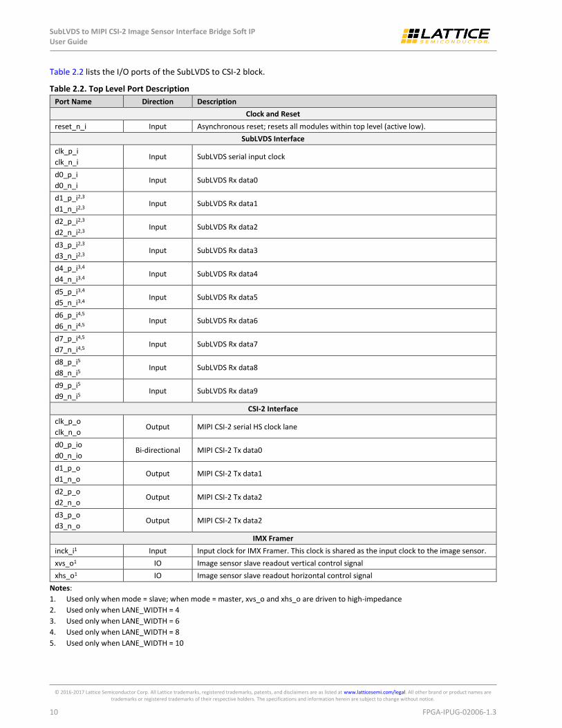
Table 2.2 lists the I/O ports of the SubLVDS to CSI-2 block.
Table 2.2. Top Level Port Description
Port Name Direction Description
Clock and Reset
reset_n_i Input Asynchronous reset; resets all modules within top level (active low).
SubLVDS Interface
clk_p_i
clk_n_i Input SubLVDS serial input clock
d0_p_i
d0_n_i Input SubLVDS Rx data0
d1_p_i2,3
d1_n_i2,3 Input SubLVDS Rx data1
d2_p_i2,3
d2_n_i2,3 Input SubLVDS Rx data2
d3_p_i2,3
d3_n_i2,3 Input SubLVDS Rx data3
d4_p_i3,4
d4_n_i3,4 Input SubLVDS Rx data4
d5_p_i3,4
d5_n_i3,4 Input SubLVDS Rx data5
d6_p_i4,5
d6_n_i4,5 Input SubLVDS Rx data6
d7_p_i4,5
d7_n_i4,5 Input SubLVDS Rx data7
d8_p_i5
d8_n_i5 Input SubLVDS Rx data8
d9_p_i5
d9_n_i5 Input SubLVDS Rx data9
CSI-2 Interface
clk_p_o
clk_n_o Output MIPI CSI-2 serial HS clock lane
d0_p_io
d0_n_io Bi-directional MIPI CSI-2 Tx data0
d1_p_o
d1_n_o Output MIPI CSI-2 Tx data1
d2_p_o
d2_n_o Output MIPI CSI-2 Tx data2
d3_p_o
d3_n_o Output MIPI CSI-2 Tx data2
IMX Framer
inck_i1 Input Input clock for IMX Framer. This clock is shared as the input clock to the image sensor.
xvs_o1 IO Image sensor slave readout vertical control signal
xhs_o1 IO Image sensor slave readout horizontal control signal
Notes:
1. Used only when mode = slave; when mode = master, xvs_o and xhs_o are driven to high-impedance
2. Used only when LANE_WIDTH = 4
3. Used only when LANE_WIDTH = 6
4. Used only when LANE_WIDTH = 8
5. Used only when LANE_WIDTH = 10

SubLVDS to MIPI CSI-2 Image Sensor Interface Bridge Soft IP User Guide
© 2016-2017 Lattice Semiconductor Corp. All Lattice trademarks, registered trademarks, patents, and disclaimers are as listed at www.latticesemi.com/legal. All other brand or product names are trademarks or registered trademarks of their respective holders. The specifications and information herein are subject to change without notice.
FPGA-IPUG-02006-1.3 11
2.3.1. SubLVDS Rx Wrapper
The sublvds_rx_wrapper module is composed of a deserializer and a word alignment module.
The deserializer converts each double data rate lane to a single data rate 8-bit or 16-bit bus at slower operating speeds within system.
The word alignment module receives the 8-bit (1:8 gearing) or 16-bit (1:16 gearing) deserialized data and converts it to 10-bit or 12-bit pixel data according to the set configuration of data type (RAW10 or RAW12). The output of the module is a multi-pixel bus, a dvalid_o, fv_o and lv_o control signal. The dvalid_o control signal goes active high on clock cycles that have valid pixel data. There is also a parser inside that looks at the recognition codes from the beginning (SAV) and the end (EAV) of each data packet if they are part of an active video line or not. The fv_o goes high at the beginning of an active video frame and low at the end of the frame. Similarly, the lv_o goes active high or low at the beginning or end of an active video line respectively.
Table 2.3. Indicator States
Sync Code FV State LV State
SAV (valid line) 1 1
EAV (valid line) 1 0
SAV (invalid line 0 0
EAV (invalid line) 0 0
2.3.2. CMOS2DPHY
The cmos_2_dphy_ip is a soft IP block that is reused in the SubLVDS-to-CSI-2 IP. This module accepts the large multiple-pixel bus from the SubLVDS Rx and serializes it into HS data packets following the MIPI CSI-2 Specification. It consists of the Pixel2byte, Packet Footer, Packet Header, Tx Global Operations Controller and D-PHY Common Interface Wrapper.
The Pixel2byte block converts the pixel data to MIPI byte data based on the number of bits per pixel, the data type and the number of MIPI D-PHY lanes that are to be used. This module should also be able to handle cases of sending in multiple pixels per clock cycle for cases where the pixel clock is too fast for the fabric.
The packet footer block generates the CRC16 checksum based on the byte data coming in and an enable. The packet header block generates and appends the packet header and footer to the data payload.
The Tx global operations controller controls HS request path and timing using parameters. Currently LP-request, escape mode and turnaround path are not supported. This block should follow the requirement from MIPI D-PHY Specification version 1.2 section 6 – Operating Modes for Control and High-Speed Data Transmission.
The D-PHY Common Interface (DCI) wrapper is used as the wrapper of the MIPI D-PHY IP. This is used to serialize the incoming byte data and transmits to D-PHY receiver. The DCI is used to make a connection between the PHY hard IP and higher protocol layers. Based on the Tx global operation state, it determines how to enable HS or LS mode for data transfer.
2.3.3. IMX Framer
The imx_framer module is for image sensors that operate in Slave mode. Image sensors that use this mode must have their XHS and XVS driven by another component. In such case, the SubLVDS-to-CSI-2 IP drives the signals in a similar manner to frame valid and line valid indicators. It provides a control mechanism for the rate at which each line and frame is read out. Timing of these two signals is defined in the Image Sensor datasheet. Timing of the XHS and XVS is shown in Figure 2.1.

SubLVDS to MIPI CSI-2 Image Sensor Interface Bridge Soft IP User Guide
© 2016-2017 Lattice Semiconductor Corp. All Lattice trademarks, registered trademarks, patents, and disclaimers are as listed at www.latticesemi.com/legal. All other brand or product names are trademarks or registered trademarks of their respective holders. The specifications and information herein are subject to change without notice.
12 FPGA-IPUG-02006-1.3
3. Parameter Settings Table 3.1 shows the user parameters used to generate the SubLVDS to MIPI CSI-2 IP.
Table 3.1. SubLVDS to CSI-2 IP Parameters
Parameter Attribute Options Description
Number of Rx lanes User Input
4 6 8 10
Selects the number of Rx SubLVDS data lanes.
Rx Gear User Input 8 16
Select gearing of Rx side. Only 4 Rx lanes support both 1:8 and 1:16 gearing. The 6, 8 and 10 Rx lanes support only 1:8 gearing.
Tx Line Rate User Input
Minimum: 320 Mb/s Maximum: 4 and 6 Rx lane – 900 Mb/s 8 Rx lane – 1440 Mb/s 10 Rx lane – 1500 Mb/s
Target Tx line rate in Mb/s. Rx line rate is not the same as Tx. Rx line rate depends on the number of Rx lanes.
Tx D-PHY Clock Mode User Input Continuous Non-continuous
Select for desired Tx clock mode. Continuous – High-speed clock only Non-continuous – High-speed and Low-power switching
tINIT_SLAVE Value User Input 1 – 32767
This parameter can be configured by the user to ensure that the initialization period of the D-PHY slave is met. The D-PHY specification places a minimum period of 100 µs, but this parameter may be increased depending on the receiver requirement. During this period, all incoming data is ignored by the bridge.
Bypass tINIT Counter User Input Enable Disable
Select this option if you want to disable or bypass the tINIT counter inside the design to save LUTs.
Miscellaneous User Input Enable Disable
If enabled, it probes internal signals for debug purposes.
Data Type User Input RAW10 RAW12
Selects desired data type.
Word Count User Input 1 – 65536
Specify the total number of bytes for active pixels in a line with the EAV (4* number of Rx lane). Word Count = ((Number of active pixel per line) + (4∙(Number of Rx lanes))∙(Bits per pixel) / 8 For example RAW10, 1920x1080p60 resolution, 10 Rx lanes: Word Count = (1920+(4∙10))∙(10) / 8 = 2450
Virtual Channel ID User Input 0 – 3 Virtual channel ID assignment for packets from channel 1
Image Sensor Mode User Input Master Slave
Set the mode of the image sensor. In slave mode, it enables the IMX framer.
V_TOTAL User Input Decimal value Set the number of lines XVS will be driven high. This parameter is needed in slave mode. When in master mode, please disregard this entry.
H_TOTAL User Input Decimal value Set the number of INCK clocks XHS will be driven high. This parameter is needed in slave mode. When in master mode, please disregard this entry.
V_H_BLANK User Input Decimal value Set the number of INCK clocks XVS and XHS will be driven low. This parameter is needed in slave mode. When in master mode, please disregard this entry.

SubLVDS to MIPI CSI-2 Image Sensor Interface Bridge Soft IP User Guide
© 2016-2017 Lattice Semiconductor Corp. All Lattice trademarks, registered trademarks, patents, and disclaimers are as listed at www.latticesemi.com/legal. All other brand or product names are trademarks or registered trademarks of their respective holders. The specifications and information herein are subject to change without notice.
FPGA-IPUG-02006-1.3 13
4. IP Generation and Evaluation This section provides information on how to generate the Lattice SubLVDS to CSI-2 IP code using the Diamond Clarity Designer, and how to run simulation, synthesis and hardware evaluation.
4.1. Licensing the IP An IP-specific license is required to enable full, unrestricted use of the SubLVDS to CSI-2 IP in a complete, top level design. The SubLVDS to CSI-2 IP is available free of charge.
Please request your free license by sending an email to [email protected] attaching your existing Lattice Diamond license or providing your MacID along with the IP details.
You may download or generate the SubLVDS to CSI-2 IP and fully evaluate the through functional simulation and implementation (synthesis, map, place and route) without the IP license. The SubLVDS to CSI-2 IP also supports Lattice’s IP hardware evaluation capability, which makes it possible to create versions of the IP that operate in hardware for a limited time (approximately four hours) without requiring an IP license. See the Hardware Evaluation section on page 23 for further details. However, the IP license is required to enable timing simulation, to open the design in Diamond EPIC tool, or to generate bitstreams that do not include the hardware evaluation timeout limitation.
4.2. Getting Started The SubLVDS to MIPI CSI-2 Image Sensor Interface Bridge is available for download from the Lattice IP Server using the Clarity Designer. The IP files are automatically installed using ispUPDATE technology in any customer-specified directory. After the IP has been installed, the IP is available in the Clarity Designer GUI as shown in Figure 4.1.
Figure 4.1. Clarity Designer Window

SubLVDS to MIPI CSI-2 Image Sensor Interface Bridge Soft IP User Guide
© 2016-2017 Lattice Semiconductor Corp. All Lattice trademarks, registered trademarks, patents, and disclaimers are as listed at www.latticesemi.com/legal. All other brand or product names are trademarks or registered trademarks of their respective holders. The specifications and information herein are subject to change without notice.
14 FPGA-IPUG-02006-1.3
4.3. Creating IP in Clarity Designer The Clarity Designer tool is used to customize modules and IPs and place them into the device’s architecture. Besides configuration and generation of modules and IPs, Clarity Designer can also create a top module template in which all generated modules and IPs are instantiated.
The following describes the procedure for generating SubLVDS to MIPI CSI-2 IP in Clarity Designer.
Clarity Designer can be started from the Diamond design environment.
To start Clarity Designer:
1. Create a new empty Diamond project for LIFMD family devices.
2. From the Diamond main window, choose Tools > Clarity Designer, or click in Diamond toolbox. The Clarity Designer project dialog box is displayed.
3. Select and or fill out the following items as shown in Figure 4.2.
Create new Clarity design — Choose to create a new Clarity Design project directory in which the SubLVDS to CSI-2 IP will be generated.
Design Location — Clarity Design project directory path.
Design Name — Clarity Design project name.
HDL Output — Hardware Description Language Output Format (Verilog).
The Clarity Designer project dialog box also allows you to open an existing Clarity Designer project by selecting the following:
Open Clarity design — Open an existing Clarity Design project.
Design File — Name of existing Clarity Design project file with .sbx extension.
4. Click the Create button. A new Clarity Designer project is created.
Figure 4.2. Starting Clarity Designer from Diamond Design Environment
SubLVDS to MIPI CSI-2 Image Sensor Interface Bridge Soft IP User Guide
© 2016-2017 Lattice Semiconductor Corp. All Lattice trademarks, registered trademarks, patents, and disclaimers are as listed at www.latticesemi.com/legal. All other brand or product names are trademarks or registered trademarks of their respective holders. The specifications and information herein are subject to change without notice.
FPGA-IPUG-02006-1.3 15
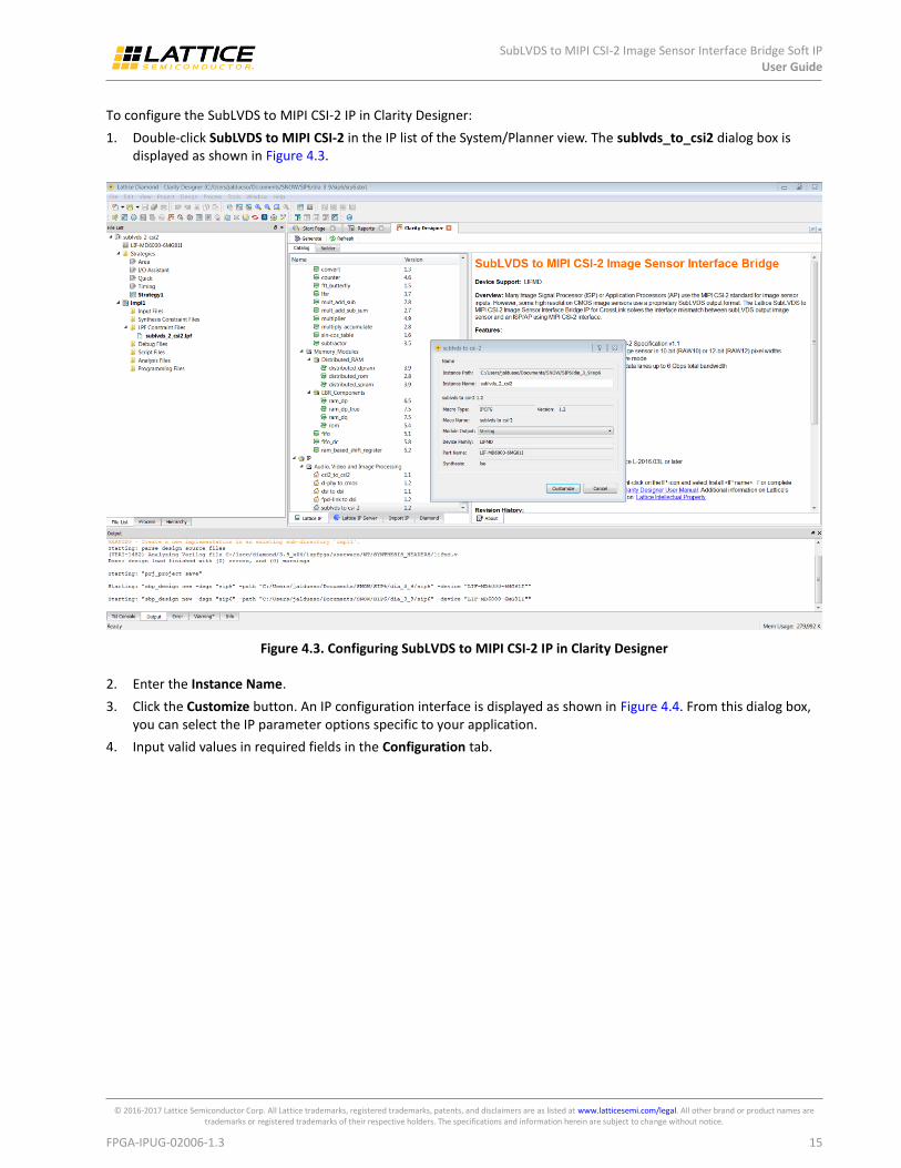
To configure the SubLVDS to MIPI CSI-2 IP in Clarity Designer:
1. Double-click SubLVDS to MIPI CSI-2 in the IP list of the System/Planner view. The sublvds_to_csi2 dialog box is displayed as shown in Figure 4.3.
Figure 4.3. Configuring SubLVDS to MIPI CSI-2 IP in Clarity Designer
2. Enter the Instance Name.
3. Click the Customize button. An IP configuration interface is displayed as shown in Figure 4.4. From this dialog box, you can select the IP parameter options specific to your application.
4. Input valid values in required fields in the Configuration tab.

SubLVDS to MIPI CSI-2 Image Sensor Interface Bridge Soft IP User Guide
© 2016-2017 Lattice Semiconductor Corp. All Lattice trademarks, registered trademarks, patents, and disclaimers are as listed at www.latticesemi.com/legal. All other brand or product names are trademarks or registered trademarks of their respective holders. The specifications and information herein are subject to change without notice.
16 FPGA-IPUG-02006-1.3
Figure 4.4. Configuration Tab in IP GUI
5. To configure data type, virtual channel ID, word count and IMX Framer settings (when image sensor is in slave mode) click the Video tab as shown in Figure 4.5.

SubLVDS to MIPI CSI-2 Image Sensor Interface Bridge Soft IP User Guide
© 2016-2017 Lattice Semiconductor Corp. All Lattice trademarks, registered trademarks, patents, and disclaimers are as listed at www.latticesemi.com/legal. All other brand or product names are trademarks or registered trademarks of their respective holders. The specifications and information herein are subject to change without notice.
FPGA-IPUG-02006-1.3 17
Figure 4.5. Video Tab in IP GUI
6. To modify D-PHY timing parameters, click the Protocol Timing Parameters tab as shown in Figure 4.6.
7. Select the required parameters, and click the Configure button.
8. Click Close.
9. Click in the toolbox. Clarity Designer generates all the IPs and modules, and creates a top module to wrap them.
For detailed instructions on how to use the Clarity Designer, refer to the Lattice Diamond software user guide.

SubLVDS to MIPI CSI-2 Image Sensor Interface Bridge Soft IP User Guide
© 2016-2017 Lattice Semiconductor Corp. All Lattice trademarks, registered trademarks, patents, and disclaimers are as listed at www.latticesemi.com/legal. All other brand or product names are trademarks or registered trademarks of their respective holders. The specifications and information herein are subject to change without notice.
18 FPGA-IPUG-02006-1.3
Figure 4.6. Protocol Timing Parameters Tab in IP GUI
SubLVDS to MIPI CSI-2 Image Sensor Interface Bridge Soft IP User Guide
© 2016-2017 Lattice Semiconductor Corp. All Lattice trademarks, registered trademarks, patents, and disclaimers are as listed at www.latticesemi.com/legal. All other brand or product names are trademarks or registered trademarks of their respective holders. The specifications and information herein are subject to change without notice.
FPGA-IPUG-02006-1.3 19
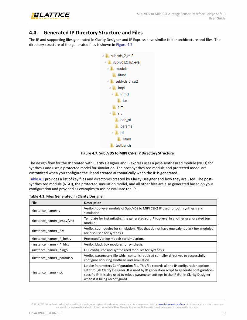
4.4. Generated IP Directory Structure and Files The IP and supporting files generated in Clarity Designer and IP Express have similar folder architecture and files. The directory structure of the generated files is shown in Figure 4.7.
Figure 4.7. SubLVDS to MIPI CSI-2 IP Directory Structure
The design flow for the IP created with Clarity Designer and IPexpress uses a post-synthesized module (NGO) for synthesis and uses a protected model for simulation. The post-synthesized module and protected model are customized when you configure the IP and created automatically when the IP is generated.
Table 4.1 provides a list of key files and directories created by Clarity Designer and how they are used. The post-synthesized module (NGO), the protected simulation model, and all other files are also generated based on your configuration and provided as examples to use or evaluate the IP.
Table 4.1. Files Generated in Clarity Designer
File Description
<instance_name>.v Verilog top-level module of SubLVDS to MIPI CSI-2 IP used for both synthesis and simulation.
<instance_name>_inst.v/vhd Template for instantiating the generated soft IP top-level in another user-created top module.
<instance_name>_*.v Verilog submodules for simulation. Files that do not have equivalent black box modules are also used for synthesis.
<instance_name>_*_beh.v Protected Verilog models for simulation.
<instance_name>_*_bb.v Verilog black box modules for synthesis.
<instance_name>_*.ngo GUI configured and synthesized modules for synthesis.
<instance_name>_params.v Verilog parameters file which contains required compiler directives to successfully configure IP during synthesis and simulation.
<instance_name>.lpc
Lattice Parameters Configuration file. This file records all the IP configuration options set through Clarity Designer. It is used by IP generation script to generate configuration-specific IP. It is also used to reload parameter settings in the IP GUI in Clarity Designer when it is being reconfigured.

SubLVDS to MIPI CSI-2 Image Sensor Interface Bridge Soft IP User Guide
© 2016-2017 Lattice Semiconductor Corp. All Lattice trademarks, registered trademarks, patents, and disclaimers are as listed at www.latticesemi.com/legal. All other brand or product names are trademarks or registered trademarks of their respective holders. The specifications and information herein are subject to change without notice.
20 FPGA-IPUG-02006-1.3
Besides the files listed in the tables, most of the files required to evaluate the SubLVDS to MIPI CSI-2 IP reside under the directory \<sublvds2csi2_eval>. This includes the simulation model, testbench and simulation script files for running the simulation in Active HDL.
The \<instance_name> folder contains files/folders with content specific to the <instance_name> configuration. This directory is created by Clarity Designer each time the IP is generated and regenerated with the same file name. A separate \<instance_name> directory is generated for IPs with different names, such as \<my_IP_0>, \<my_IP_1>, and others.
The folder\<instance_name>, the \sublvds2csi2_eval and subtending directories provide files supporting SubLVDS to CSI-2 IP evaluation that includes files/folders with content that is constant for all configurations of the SubLVDS to MIPI CSI-2 IP. The \sublvds2csi2_eval directory is created by Clarity Designer the first time the IP is generated when multiple SubLVDS to MIPI CSI-2 IP are generated in the same root directory and updated each time the IP is regenerated.
The simulation part of the user evaluation provides testbench and test cases supporting RTL simulation for Active-HDL simulators under <project root>\testbench.
Separate directories located at \<project_dir>\sublvds2csi2_eval\<instance_name>\sim\Aldec\rtl are provided and contain pre-built simulation script files.
4.5. Running Functional Simulation The functional simulation includes a configuration-specific behavioral model of the SubLVDS to CSI-2 Image Sensor Interface Bridge, which is instantiated in an FPGA top level along with some other logic (such as PLLs and registers with Read/Write Interface). This FPGA top is instantiated in an evaluation testbench that provides appropriate stimulus for the SubLVDS to CSI-2 Bridge. The testbench files are provided in <project_dir>\sublvds2csi2_eval\testbench.
The generated IP package includes the configuration-specific behavior model (<instance_name>_beh.v, provided in <project_dir>\sublvds2csi2_eval\<instance_name>\src\beh_rtl\<family>) for functional simulation. Models for simulation are provided in the corresponding \models folder if required.
To run the simulation in Active-HDL (Windows only) follow these steps:
1. Modify the *.do file located in \<project_dir>\<IPinstance_name>\<instance_name>_eval\<IPinstance_name>\sim\aldec\
a. Specify working directory (sim_working_folder) , for example
set sim_working_folder "C:/my_design"
b. Specify workspace name that will be created in working directory, for example
set workspace_name "design_space"
c. Specify design name, for example
set design_name "DesignA"
d. Specify design path where the IP Core generated using Clarity Designer is located, for example
set design_path "C:/my_designs/DesignA"
e. Specify design instance name (same as the instance name specified in Clarity Designer), for example
set design_inst "DesignA_inst"
f. Specify Lattice Diamond primitive path (diamond_dir) to where it is installed, for example
set diamond_dir "C:/lscc/diamond/3.8_x64"
2. Update testbench parameters to customize data size, clock and/or other settings. Table 4.2 for the list of valid testbench compiler directives .
3. Under the Tools menu, select Active-HDL.
4. In Active-HDL window, click Tools -> Execute macro.
5. Select the *.do file.
6. Wait for the simulation to finish.
SubLVDS to MIPI CSI-2 Image Sensor Interface Bridge Soft IP User Guide
© 2016-2017 Lattice Semiconductor Corp. All Lattice trademarks, registered trademarks, patents, and disclaimers are as listed at www.latticesemi.com/legal. All other brand or product names are trademarks or registered trademarks of their respective holders. The specifications and information herein are subject to change without notice.
FPGA-IPUG-02006-1.3 21
Table 4.2 is a list of testbench directives which can be modified by setting the define in the vlog command in the *.do file.
Example:
vlog \
+define+NUM_FRAMES=60 \
+define+NUM_LINES=1080 \
....
Table 4.2. Testbench Directives
Directive Description
NUM_PIXELS Number of pixels per line
NUM_LINES Number of lines per frame
NUM_FRAMES Number of frames to be transmitted
VFRONT_BLNK Vertical front blanking
VREAR_BLNK Vertical rear blanking
XHS_ASRT Number of clock DCK cycles the xhs signal is asserted
XHS_PERIOD XHS period in terms of DCK cycles
INIT_DRIVE_DELAY Delay from reset deassertion or tinit_done assertion before model starts driving data
FRAMER Used to enable sampling of xhs and xvs when design is in slave mode
Users can override the default timing parameters using the above information.
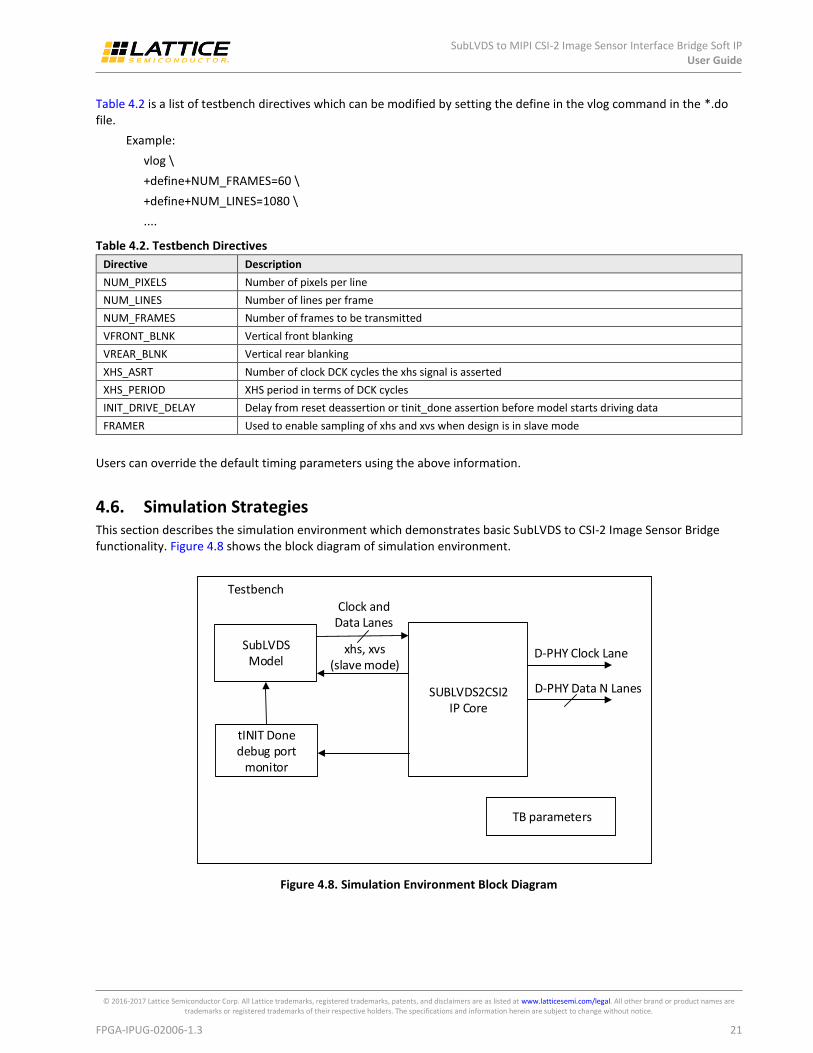
4.6. Simulation Strategies This section describes the simulation environment which demonstrates basic SubLVDS to CSI-2 Image Sensor Bridge functionality. Figure 4.8 shows the block diagram of simulation environment.
SubLVDSModel
SUBLVDS2CSI2IP Core
tINIT Done debug port
monitor
Clock and Data Lanes
Testbench
D-PHY Data N Lanes
TB parameters
D-PHY Clock Lanexhs, xvs (slave mode)
Figure 4.8. Simulation Environment Block Diagram
SubLVDS to MIPI CSI-2 Image Sensor Interface Bridge Soft IP User Guide
© 2016-2017 Lattice Semiconductor Corp. All Lattice trademarks, registered trademarks, patents, and disclaimers are as listed at www.latticesemi.com/legal. All other brand or product names are trademarks or registered trademarks of their respective holders. The specifications and information herein are subject to change without notice.
22 FPGA-IPUG-02006-1.3
4.7. Simulation Environment The simulation environment is made up of a SubLVDS model instance connected to the input of SUBLVDS2CSI2 IP core instance in the testbench. The SubLVDS model is configured based on the SUBLVDS2CSI2 IP configurations and testbench parameters. It can be configured as 4, 6, 8 or 10 Rx lanes. If miscellaneous signals are enabled, the testbench monitors the assertion of tinit_done signal before transmitting the sublvds data to the input of the design.
The testbench also provides xhs and xvs signals to the SubLVDS model when the design is configured as master mode. Otherwise, the model will use the xhs and xvs signals from the design as reference for data transmission when configured as slave mode. Refer to testbench readme.txt file for details on how to set the TB parameters.
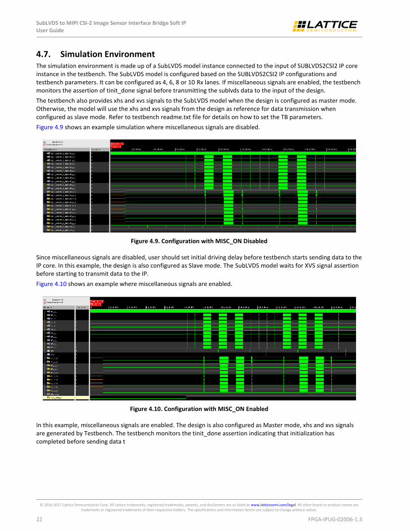
Figure 4.9 shows an example simulation where miscellaneous signals are disabled.
Figure 4.9. Configuration with MISC_ON Disabled
Since miscellaneous signals are disabled, user should set initial driving delay before testbench starts sending data to the IP core. In this example, the design is also configured as Slave mode. The SubLVDS model waits for XVS signal assertion before starting to transmit data to the IP.
Figure 4.10 shows an example where miscellaneous signals are enabled.
Figure 4.10. Configuration with MISC_ON Enabled
In this example, miscellaneous signals are enabled. The design is also configured as Master mode, xhs and xvs signals are generated by Testbench. The testbench monitors the tinit_done assertion indicating that initialization has completed before sending data t

SubLVDS to MIPI CSI-2 Image Sensor Interface Bridge Soft IP User Guide
© 2016-2017 Lattice Semiconductor Corp. All Lattice trademarks, registered trademarks, patents, and disclaimers are as listed at www.latticesemi.com/legal. All other brand or product names are trademarks or registered trademarks of their respective holders. The specifications and information herein are subject to change without notice.
FPGA-IPUG-02006-1.3 23
4.8. Instantiating the IP The core modules of SubLVDS to CSI-2 IP are synthesized and provided in NGO format with black box Verilog source files for synthesis. A Verilog source file named <instance_name>_sublvds_2_csi2_ip.v instantiates the black box of core modules. The top-level file <instance_name>.v instantiates <instance_name>_sublvds_2_csi2_ip.v.
The IP instances do not need to be instantiated one by one manually. The top-level file and the other Verilog source files are provided in \<project_dir>. These files are refreshed each time the IP is regenerated.
For example, if the Clarity Designer project file is cdprj.sbx, the automatically generated wrapper file is cdprj.v in which all generated IPs are instantiated. The user does not need to instantiate the IP instances one by one manually. The cdprj.v is refreshed each time the IPs in the design are regenerated.
A Verilog instance template <instance_name>_inst.v or VHDL instance template <instance_name>_inst.vhd is also provided as a guide if the design is to be included in another top level module.
4.9. Synthesizing and Implementing the IP in a Top-Level Design In Clarity Designer, the Clarity Designer project file (.sbx) is added to Lattice Diamond as a source file after all IPs are generated. Note that default Diamond strategy (.sty) and default Diamond preference file (.lpf) are used. When using .sbx approach, import the recommended strategy and preferences from \<project_dir>\sublvds2csi2_eval\<instance_name>\impl\lifmd\[lse | synplify] directories.
All required files are invoked automatically. You can directly synthesize, map and place/par the design in the Diamond design environment after the IPsare generated.
To use the project files in Diamond:
1. Choose File > Open > Project.
2. in the Open Project dialog box browse to \<project_dir>\sublvds2csi2_eval\<instance_name>\impl\lifmd\[lse|synplify]\.
3. Select and open <instance_name>_top.ldf. At this point, all of the files needed to support top-level synthesis and implementation are imported to the project.
4. Select the Process tab in the left-hand GUI window.
5. Implement the complete design via the standard Diamond GUI flow.
4.10. Hardware Evaluation The SubLVDS to MIPI CSI-2 Image Sensor Interface Bridge IP supports Lattice’s IP hardware evaluation capability, which makes it possible to create versions of the IP that operate in hardware for a limited period of time (approximately four hours) without requiring the request of an IP license. It may also be used to evaluate the IP in hardware in user-defined designs.
4.10.1. Enabling Hardware Evaluation in Diamond
Choose Project > Active Strategy > Translate Design Settings. The hardware evaluation capability may be enabled or disabled in the Strategy dialog box. It is enabled by default.

SubLVDS to MIPI CSI-2 Image Sensor Interface Bridge Soft IP User Guide
© 2016-2017 Lattice Semiconductor Corp. All Lattice trademarks, registered trademarks, patents, and disclaimers are as listed at www.latticesemi.com/legal. All other brand or product names are trademarks or registered trademarks of their respective holders. The specifications and information herein are subject to change without notice.
24 FPGA-IPUG-02006-1.3
4.11. Updating/Regenerating the IP The Clarity Designer interface allows you to update the local IPs from the Lattice IP server. The updated IP can be used to regenerate the IP instance in the design. To change the parameters of the IP used in the design, the IP must also be regenerated.
4.11.1. Regenerating an IP in Clarity Designer
To regenerate IP in Clarity Designer:
1. In the Builder or Planner tab, right-click the IP instance to be regenerated and select Config in the menu as shown in Figure 4.11.
2. The IP Configuration GUI is displayed. Change the parameters as required and click the Configure button.
3. Update the pin connection in Builder tab for configuration changes.
4. Click in the toolbox. Clarity Designer regenerates all the instances which are reconfigured.
Figure 4.11. IP Regeneration in Clarity Designer

SubLVDS to MIPI CSI-2 Image Sensor Interface Bridge Soft IP User Guide
© 2016-2017 Lattice Semiconductor Corp. All Lattice trademarks, registered trademarks, patents, and disclaimers are as listed at www.latticesemi.com/legal. All other brand or product names are trademarks or registered trademarks of their respective holders. The specifications and information herein are subject to change without notice.
FPGA-IPUG-02006-1.3 25
References For more information about CrossLink devices, refer to FPGA-DS-02007, CrossLink Family Data Sheet
For further information on interface standards refer to:
MIPI Alliance Specification for D-PHY, version 1.1, November 7, 2011, www.mipi.org
MIPI Alliance Specification for Camera Serial Interface 2 (CSI-2) version 1.1, July 18, 2012, www.mipi.org
Technical Support Assistance Submit a technical support case through www.latticesemi.com/techsupport.

SubLVDS to MIPI CSI-2 Image Sensor Interface Bridge Soft IP User Guide
© 2016-2017 Lattice Semiconductor Corp. All Lattice trademarks, registered trademarks, patents, and disclaimers are as listed at www.latticesemi.com/legal. All other brand or product names are trademarks or registered trademarks of their respective holders. The specifications and information herein are subject to change without notice.
26 FPGA-IPUG-02006-1.3
Appendix A. Resource Utilization Table A.1 lists resource utilization for Lattice CrossLink FPGAs using the SubLVDS to MIPI CSI-2 Image Sensor Interface Bridge IP. The performance and utilization data target an LIF-MD6000-6MG81I device with –6 speed grade using Lattice Diamond 3.8 and Lattice Synthesis Engine. Performance may vary when using a different software version or targeting a different device density or speed grade within the CrossLink family. The values of fMAX shown are based on continuous byte clock. The Target fMAX column shows target byte clock frequency for each configuration.
Table A.1. Resource Utilization*
IP User-Configurable Parameters (1:8 gearing)
Slices LUTs Registers sysMEM EBRs Actual fMAX
(MHz)
Target fMAX
(MHz)
10-lane configuration 2386 3682 1758 12 96.516 93.75
8-lane configuration 1857 2466 1524 10 112.969 90
6-lane configuration 1806 2370 1385 8 116.523 112.5
4-lane configuration 1389 1878 1173 6 114.142 112.5
*Note: fMAX shown is the byte clock frequency. The target fMAX for this design is 93.75 MHz.

SubLVDS to MIPI CSI-2 Image Sensor Interface Bridge Soft IP User Guide
© 2016-2017 Lattice Semiconductor Corp. All Lattice trademarks, registered trademarks, patents, and disclaimers are as listed at www.latticesemi.com/legal. All other brand or product names are trademarks or registered trademarks of their respective holders. The specifications and information herein are subject to change without notice.
FPGA-IPUG-02006-1.3 27
Appendix B. What is Not Supported The subLVDS to MIPI CSI-2 Image Sensor Interface Bridge IP does not support the following features:
Back-to-back transition from low-power (LP) mode to high-speed (HS) mode and vice versa. There is a wait time needed between any LP and HS transition. Because of this wait time requirement on the MIPI D-PHY Tx side of the bridge, the 1st line of each frame is dropped through the bridge. The wait time (horizontal blanking period) between start of FV (frame valid) and start of LV (line valid), end of LV and end of FV, and end of LV and start of LV can be as long as 200 byte clock cycles or 650 input clock cycles depending on the lane rate.
ECC error detection and correction
Checksum error detection

SubLVDS to MIPI CSI-2 Image Sensor Interface Bridge Soft IP User Guide
© 2016-2017 Lattice Semiconductor Corp. All Lattice trademarks, registered trademarks, patents, and disclaimers are as listed at www.latticesemi.com/legal. All other brand or product names are trademarks or registered trademarks of their respective holders. The specifications and information herein are subject to change without notice.
28 FPGA-IPUG-02006-1.3
Revision History
Date Version Change Summary
February 2017 1.3 Updated the number of LUTs and Registers in Table 1.1. SubLVDS to MIPI CSI-2 IP Quick Facts
Added Tx D-PHY Clock Mode and Bypass tINIT Counter in Table 3.1. SubLVDS to CSI-2 IP Parameters
Updated figures in Getting Started and Creating IP in Clarity Designer sections
Updated resource utilization values in Table A.1. Resource Utilization
November 2016 1.2 Updated Word Count description in Table 3.1. SubLVDS to CSI-2 IP Parameters
Updated Licensing the IP section – Added email address [email protected] for requesting free license
Added step 9 in Creating IP in Clarity Designer section
Added PLL frequency holes to the list of limitations in Appendix B. What is Not Supported
July 2016 1.1 Updated document number, the previous document number was IPUG125
Updated Synplify Pro version in Table 1.1. SubLVDS to MIPI CSI-2 IP Quick Facts, and added simulation
Updated description of Rx Gear in Table 3.1. SubLVDS to CSI-2 IP Parameters
Updated Figure 4.4. Configuration Tab in IP GUI and Figure 4.5. Video Tab in IP GUI
New Figure 4.6. Protocol Timing Parameters Tab in IP GUI
Updated Generated IP Directory Structure and Files section
New Running Functional Simulation, Simulation Strategies, Simulation Environment sections
May 2016 1.0 Initial release.

7th Floor, 111 SW 5th Avenue
Portland, OR 97204, USA
T 503.268.8000
www.latticesemi.com